scanning acoustic tomograph - hdi solutionsscanning acoustic tomograph the ultrasonic imaging device...
TRANSCRIPT
Scanning Acoustic Tomograph
http://www.hkft.co.jp
Technical data
What can be achieved?
What is Ultrasound? ………………………………………………………… 1
Characteristics of Ultrasound ……………………………………………… 1
Application Examples for Target Finding and Flaw Detection ………… 2
Notes on X-Ray and SAT Inspection Techniques ………………………… 10
Scanning Acoustic Tomograph ……………………………………………… 11
Images Acquired by Scanning Acoustic Tomograph System …………… 13
Detectability and Resolution ………………………………………………… 18
Contents
Page
1
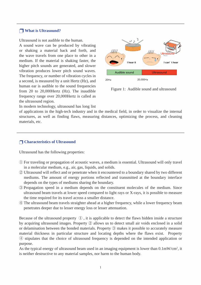
Ultrasound is not audible to the human. A sound wave can be produced by vibrating or shaking a material back and forth, and the wave travels from one place to other in a medium. If the material is shaking faster, the higher pitch sounds are generated, and slower vibration produces lower pitch sound waves. The frequency, or number of vibration cycles in a second, is measured by a unit Hertz (Hz), and human ear is audible to the sound frequencies from 20 to 20,000Hertz (Hz). The inaudible frequency range over 20,000Hertz is called as the ultrasound region. In modern technology, ultrasound has long list of applications in the high-tech industry and in the medical field, in order to visualize the internal structures, as well as finding flaws, measuring distances, optimizing the process, and cleaning materials, etc.
❐ Characteristics of Ultrasound
Ultrasound has the following properties:
① For traveling or propagation of acoustic waves, a medium is essential. Ultrasound will only travel in a molecular medium, e.g., air, gas, liquids, and solids.
② Ultrasound will reflect and or penetrate when it encountered to a boundary shared by two different mediums. The amount of energy portions reflected and transmitted at the boundary interface depends on the types of mediums sharing the boundary.
③ Propagation speed in a medium depends on the constituent molecules of the medium. Since ultrasound beam travels at lower speed compared to light rays or X-rays, it is possible to measure the time required for its travel across a smaller distance.
④ The ultrasound beam travels straighter ahead at a higher frequency, while a lower frequency beam penetrates deeper due to lesser energy loss or lesser attenuation.
Because of the ultrasound property ① , it is applicable to detect the flaws hidden inside a structure by acquiring ultrasound images. Property ② allows us to detect small air voids enclosed in a solid or delamination between the bonded materials. Property ③ makes it possible to accurately measure material thickness in particular structure and locating depths where the flaws exist. Property ④ stipulates that the choice of ultrasound frequency is depended on the intended application or purpose. As the typical energy of ultrasound beam used in an imaging equipment is lower than 0.1mW/cm2, it is neither destructive to any material samples, nor harm to the human body.
Audible sound Ultrasound
I can’ t hearI hear it
UltrasoundUltrasound
Figure 1: Audible sound and ultrasound
❐ What is Ultrasound?
2
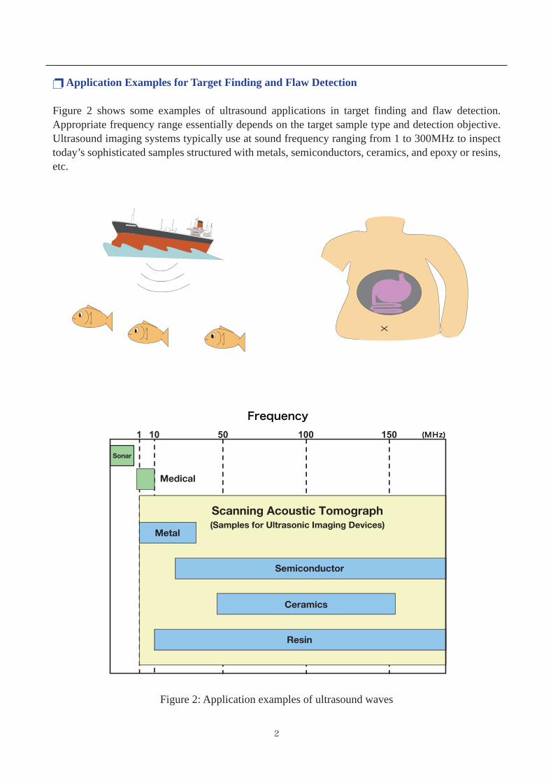
❐ Application Examples for Target Finding and Flaw Detection
Figure 2 shows some examples of ultrasound applications in target finding and flaw detection. Appropriate frequency range essentially depends on the target sample type and detection objective. Ultrasound imaging systems typically use at sound frequency ranging from 1 to 300MHz to inspect today’s sophisticated samples structured with metals, semiconductors, ceramics, and epoxy or resins, etc.
Figure 2: Application examples of ultrasound waves
Ceramics
Frequency
Sonar
Medical
Metal
Semiconductor
Resin
(Samples for Ultrasonic Imaging Devices)
Scanning Acoustic Tomograph
(MHz)
3
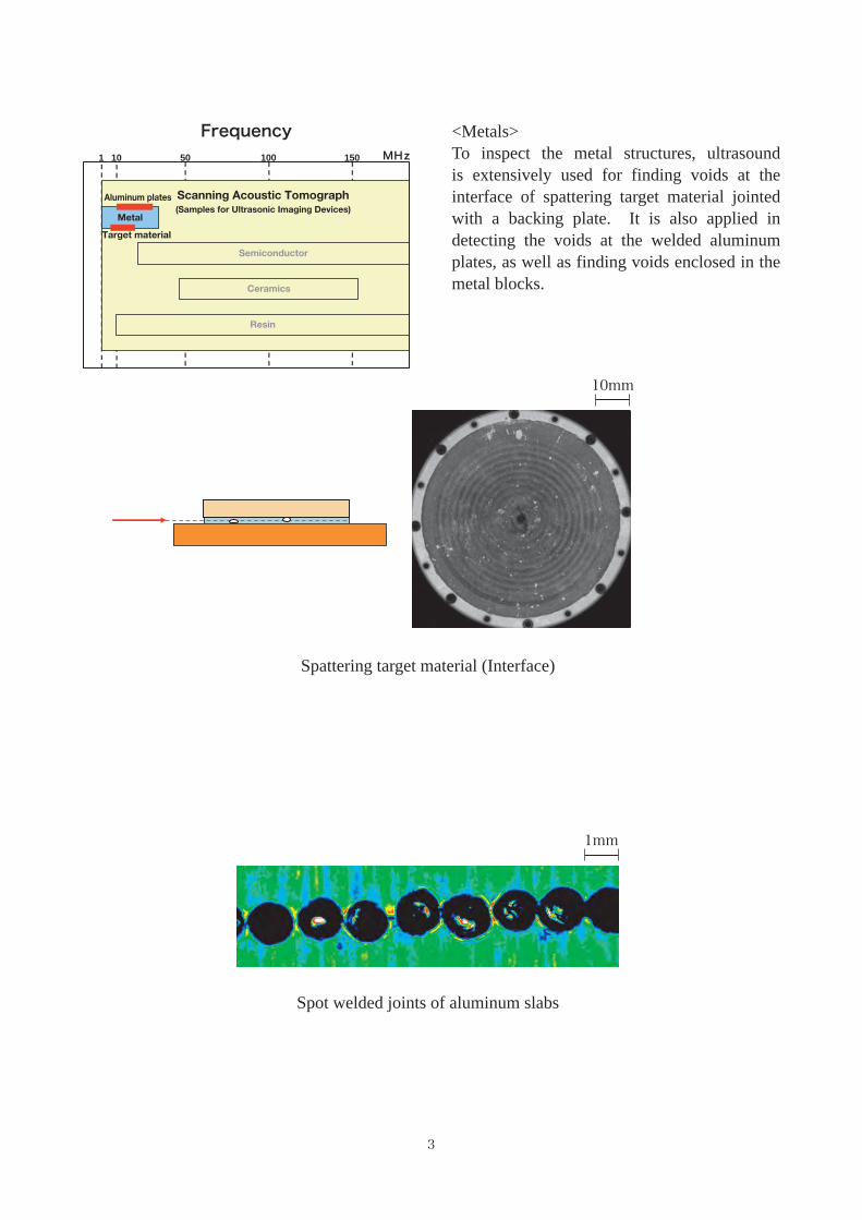
<Metals>To inspect the metal structures, ultrasound is extensively used for finding voids at the interface of spattering target material jointed with a backing plate. It is also applied in detecting the voids at the welded aluminum plates, as well as finding voids enclosed in the metal blocks.
MHz1 10 50 100 150
Semiconductor
Ceramics
Resin
(Samples for Ultrasonic Imaging Devices)
Scanning Acoustic Tomograph
Metal
Target material
Aluminum plates
Spattering target material (Interface)
Spot welded joints of aluminum slabs
Frequency
10mm
1mm
4
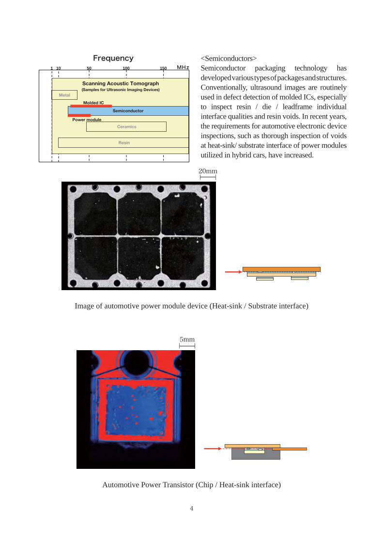
<Semiconductors>Semiconductor packaging technology has developed various types of packages and structures. Conventionally, ultrasound images are routinely used in defect detection of molded ICs, especially to inspect resin / die / leadframe individual interface qualities and resin voids. In recent years, the requirements for automotive electronic device inspections, such as thorough inspection of voids at heat-sink/ substrate interface of power modules utilized in hybrid cars, have increased.
MHz1 10 50 100
超 音 波 映 像 装 置
150
Power module
Molded IC
Metal
Semiconductor
Ceramics
Resin
(Samples for Ultrasonic Imaging Devices)Scanning Acoustic Tomograph
Image of automotive power module device (Heat-sink / Substrate interface)
Automotive Power Transistor (Chip / Heat-sink interface)
Frequency
20mm
5mm
5
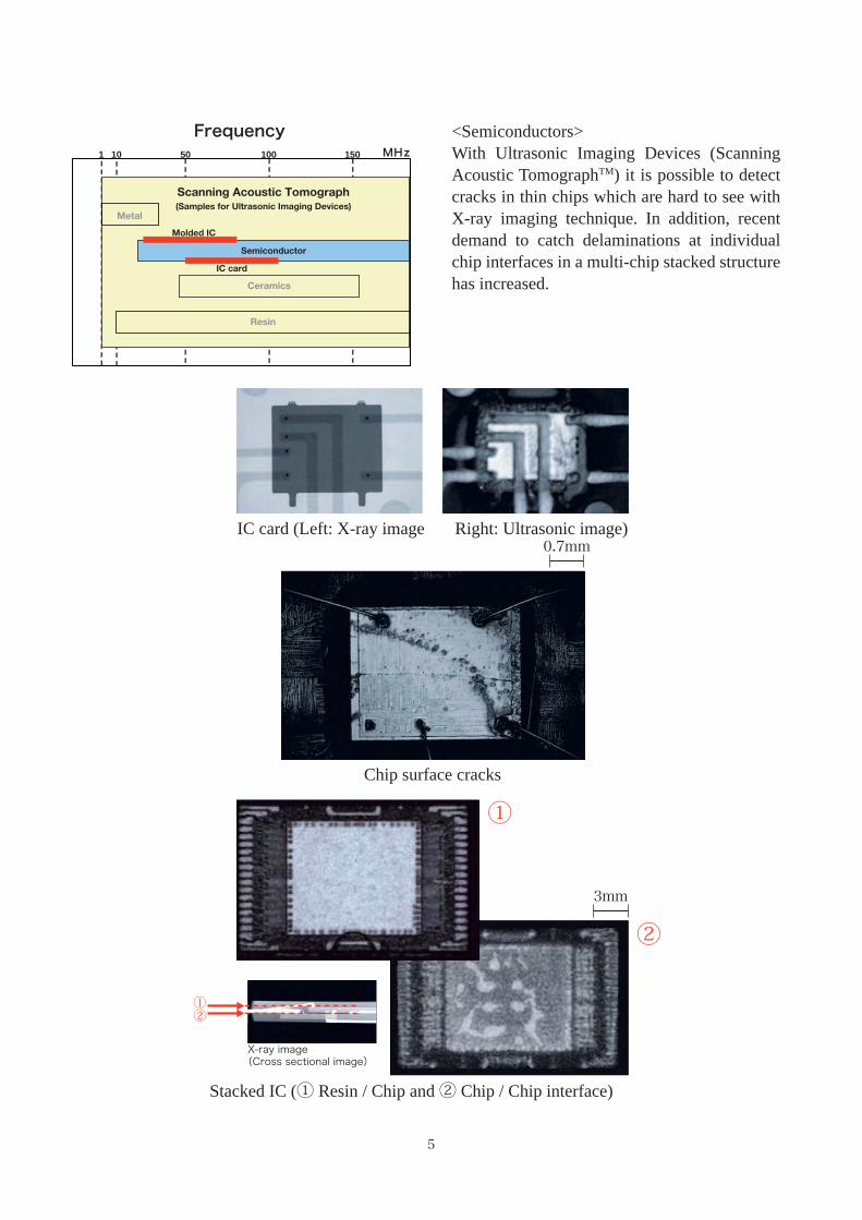
<Semiconductors>With Ultrasonic Imaging Devices (Scanning Acoustic TomographTM) it is possible to detect cracks in thin chips which are hard to see with X-ray imaging technique. In addition, recent demand to catch delaminations at individual chip interfaces in a multi-chip stacked structure has increased.
MHz1 10 50 100 150
Molded IC
(Samples for Ultrasonic Imaging Devices)
Scanning Acoustic Tomograph
Metal
Semiconductor
Ceramics
Resin
IC card
IC card (Left: X-ray image Right: Ultrasonic image)
Chip surface cracks
Stacked IC (① Resin / Chip and ② Chip / Chip interface)
X-ray image(Cross sectional image)
Frequency
0.7mm
3mm
①②
①
②
6
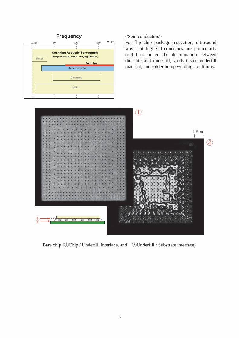
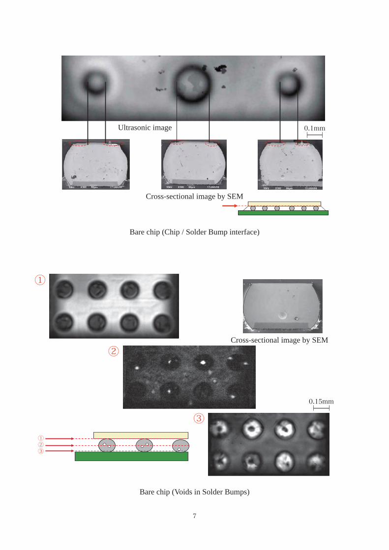
<Semiconductors>For flip chip package inspection, ultrasound waves at higher frequencies are particularly useful to image the delamination between the chip and underfill, voids inside underfill material, and solder bump welding conditions.
MHz1 10 50 100 150
Metal
Semiconductor
Ceramics
Resin
(Samples for Ultrasonic Imaging Devices)
Scanning Acoustic Tomograph
Bare chip
Bare chip (①Chip / Underfill interface, and ②Underfill / Substrate interface)
Frequency
1.5mm
①②
①
②
7
Bare chip (Chip / Solder Bump interface)
Bare chip (Voids in Solder Bumps)
Ultrasonic image
Cross-sectional image by SEM
Cross-sectional image by SEM
0.1mm
0.15mm
①②③
①
②
③
8
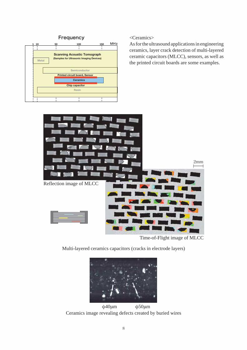
<Ceramics>As for the ultrasound applications in engineering ceramics, layer crack detection of multi-layered ceramic capacitors (MLCC), sensors, as well as the printed circuit boards are some examples.
Ceramics image revealing defects created by buried wires
Multi-layered ceramics capacitors (cracks in electrode layers)
MHz1 10 50 100 150
Metal
Semiconductor
Ceramics
Resin
(Samples for Ultrasonic Imaging Devices)
Scanning Acoustic Tomograph
Printed circuit board, Sensor
Chip capacitor
Frequency
Time-of-Flight image of MLCC
Reflection image of MLCC
φ40μm φ50μm
2mm
9
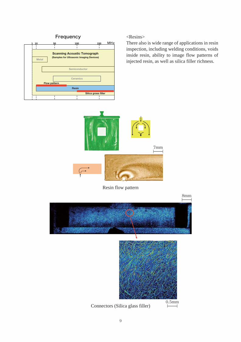
<Resins>There also is wide range of applications in resin inspection, including welding conditions, voids inside resin, ability to image flow patterns of injected resin, as well as silica filler richness.
Resin flow pattern
Connectors (Silica glass filler)
MHz1 10 50 100
超 音 波 映 像 装 置
150
Metal
Semiconductor
Ceramics
Resin
(Samples for Ultrasonic Imaging Devices)
Scanning Acoustic Tomograph
Silica grass filler
Flow pattern
Frequency
7mm
8mm
0.5mm
10
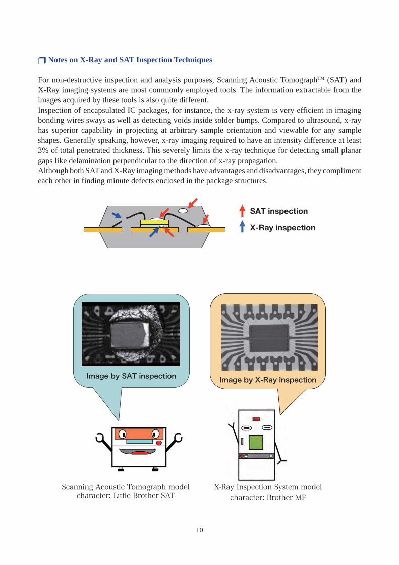
❐ Notes on X-Ray and SAT Inspection Techniques
Scanning Acoustic Tomograph model character: Little Brother SAT
X-Ray Inspection System model character: Brother MF
For non-destructive inspection and analysis purposes, Scanning Acoustic TomographTM (SAT) and X-Ray imaging systems are most commonly employed tools. The information extractable from the images acquired by these tools is also quite different.Inspection of encapsulated IC packages, for instance, the x-ray system is very efficient in imaging bonding wires sways as well as detecting voids inside solder bumps. Compared to ultrasound, x-ray has superior capability in projecting at arbitrary sample orientation and viewable for any sample shapes. Generally speaking, however, x-ray imaging required to have an intensity difference at least 3% of total penetrated thickness. This severely limits the x-ray technique for detecting small planar gaps like delamination perpendicular to the direction of x-ray propagation.Although both SAT and X-Ray imaging methods have advantages and disadvantages, they compliment each other in finding minute defects enclosed in the package structures.
SAT inspection
X-Ray inspection
Image by SAT inspection Image by X-Ray inspection
11
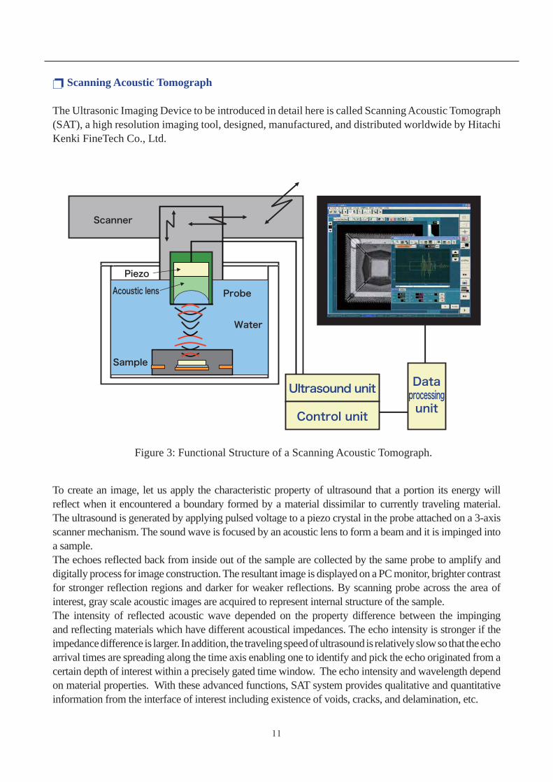
❐ Scanning Acoustic Tomograph
The Ultrasonic Imaging Device to be introduced in detail here is called Scanning Acoustic Tomograph (SAT), a high resolution imaging tool, designed, manufactured, and distributed worldwide by Hitachi Kenki FineTech Co., Ltd.
Figure 3: Functional Structure of a Scanning Acoustic Tomograph.
To create an image, let us apply the characteristic property of ultrasound that a portion its energy will reflect when it encountered a boundary formed by a material dissimilar to currently traveling material. The ultrasound is generated by applying pulsed voltage to a piezo crystal in the probe attached on a 3-axis scanner mechanism. The sound wave is focused by an acoustic lens to form a beam and it is impinged into a sample. The echoes reflected back from inside out of the sample are collected by the same probe to amplify and digitally process for image construction. The resultant image is displayed on a PC monitor, brighter contrast for stronger reflection regions and darker for weaker reflections. By scanning probe across the area of interest, gray scale acoustic images are acquired to represent internal structure of the sample.The intensity of reflected acoustic wave depended on the property difference between the impinging and reflecting materials which have different acoustical impedances. The echo intensity is stronger if the impedance difference is larger. In addition, the traveling speed of ultrasound is relatively slow so that the echo arrival times are spreading along the time axis enabling one to identify and pick the echo originated from a certain depth of interest within a precisely gated time window. The echo intensity and wavelength depend on material properties. With these advanced functions, SAT system provides qualitative and quantitative information from the interface of interest including existence of voids, cracks, and delamination, etc.
Scanner
Probe
Piezo
Water
Sample
Acoustic lens
Ultrasound unit
Control unit
Dataprocessingunit
12
Table 1: Sound velocity, Wavelength, Acoustical impedance and Reflectivity
Sound velocity (Longitudinal wave): C= (m/s)
Wavelength: λ= C/f(mm)
Acoustic impedance: Z = ρ・C
Ref lectivity: R=(Z2-Z1)/(Z2+Z1)
Where E :Young’s Modulus, σ:Poisson’s Ratio, ρ:Density,f:Frequency, Z1:Acoustic impedance of incidence side material Z2:Acoustic impedance of reflecting side material
E(1-σ)ρ(1+σ)·(1-2σ)
Scanning Acoustic Tomograph FineSAT (Type II)
m/s(25MHz)
mm
Acousticimpedance10kg/m2s Silicon Metal Resin Water
Air
Water
Resin
Metal
Silicon
Material
344
1480
3930
5900
8600
0.01
0.03
0.16
0.24
0.34
0.0
1.5
6.8
45.4
20
100
86
50
39
100
93
74
100
64
100
Soundvelocity
( Longitudinal wave )
Wavelength Reflectivity %
13
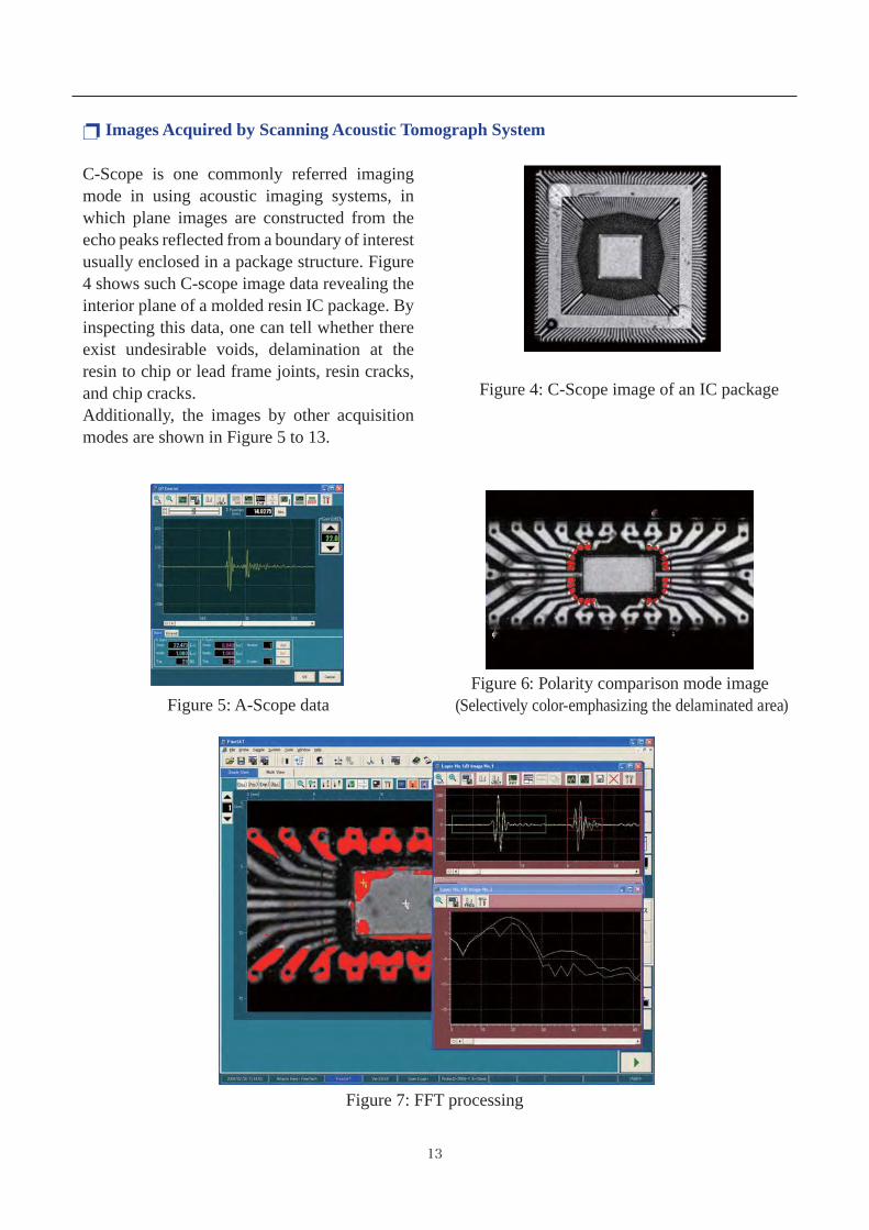
❐ Images Acquired by Scanning Acoustic Tomograph System
C-Scope is one commonly referred imaging mode in using acoustic imaging systems, in which plane images are constructed from the echo peaks reflected from a boundary of interest usually enclosed in a package structure. Figure 4 shows such C-scope image data revealing the interior plane of a molded resin IC package. By inspecting this data, one can tell whether there exist undesirable voids, delamination at the resin to chip or lead frame joints, resin cracks, and chip cracks.Additionally, the images by other acquisition modes are shown in Figure 5 to 13.
Figure 7: FFT processing
Figure 4: C-Scope image of an IC package
Figure 5: A-Scope dataFigure 6: Polarity comparison mode image
(Selectively color-emphasizing the delaminated area)

14
The A-Scope mode shown in Figure 5 is not only very useful for adjusting focus point, determining the depth of interest or gate width and height settings, but also measuring sound velocity and distances, quick confirmation of echo characteristics on each point of interest including intensities and phases that appears to reverse when ultrasound wave impinged from higher to lower impedance material. In Figure 6, we use the polarity inversion characteristics to emphasize delaminated region coded by colors: this mode of imaging is also known as Polarity Comparison Mode (PCM) as patented by Hitachi. Moreover, the same A-scope data can also be processed by using FFT frequency domain analysis as shown in Figure 7, to reveal the difference in number of peaks associated to the echoes of different sites.
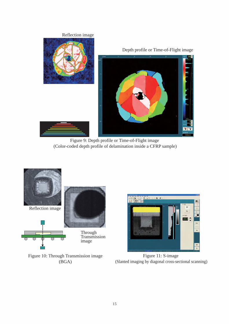
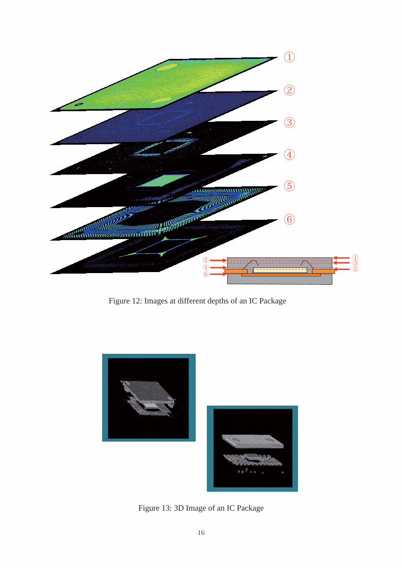
Figure 8 shows a B-scope or cross-sectional image data, with which resin crack advancing directions and depth locations of voids can be inspected. Figure 9 is created from depth profile data by color-coding of different depths. Figure 10 show the reflection and transmission images of multi-layer BGA package. The S-image shown in Figure 11 is another innovation by Hitachi to first image a sample diagonally so that target depth can be quickly focused by a mouse click and other measurement parameters can also be easily optimized. Figure 12 is called Lamino image where individual layers of different depths can be imaged by a single pass. Figure 13 shows the 3D image obtained by volumetric scanning that acquires all the waveform data from all points.
Figure 8: B-scope image (Cross sectional image)
Surface
ChipWire
Leadframe
15
Figure 9: Depth profile or Time-of-Flight image (Color-coded depth profile of delamination inside a CFRP sample)
Figure 10: Through Transmission image (BGA)
Figure 11: S-image (Slanted imaging by diagonal cross-sectional scanning)
Reflection image
Reflection image
Depth profile or Time-of-Flight image
Through Transmission image
16
Figure 12: Images at different depths of an IC Package
Figure 13: 3D Image of an IC Package
①③⑤
②④⑥
①
②
③
④
⑤
⑥
17
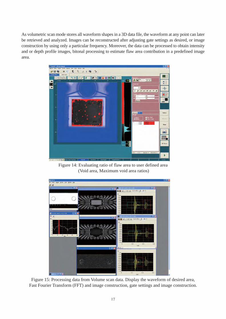
As volumetric scan mode stores all waveform shapes in a 3D data file, the waveform at any point can later be retrieved and analyzed. Images can be reconstructed after adjusting gate settings as desired, or image construction by using only a particular frequency. Moreover, the data can be processed to obtain intensity and or depth profile images, bitonal processing to estimate flaw area contribution in a predefined image area.
Figure 14: Evaluating ratio of flaw area to user defined area (Void area, Maximum void area ratios)
Figure 15: Processing data from Volume scan data. Display the waveform of desired area, Fast Fourier Transform (FFT) and image construction, gate settings and image construction.
18
❐ Detectability and Resolution
The detectability and resolution of a Scanning Acoustic Tomograph system depends on:・ Probe frequency, focal length, damping characteristics・ Bandwidth of ultrasonic flaw detection system, linearity in signal amplification electronics・ Accuracy and Precision of positioning scanner・ Measurement conditions・ Sample shape and material type
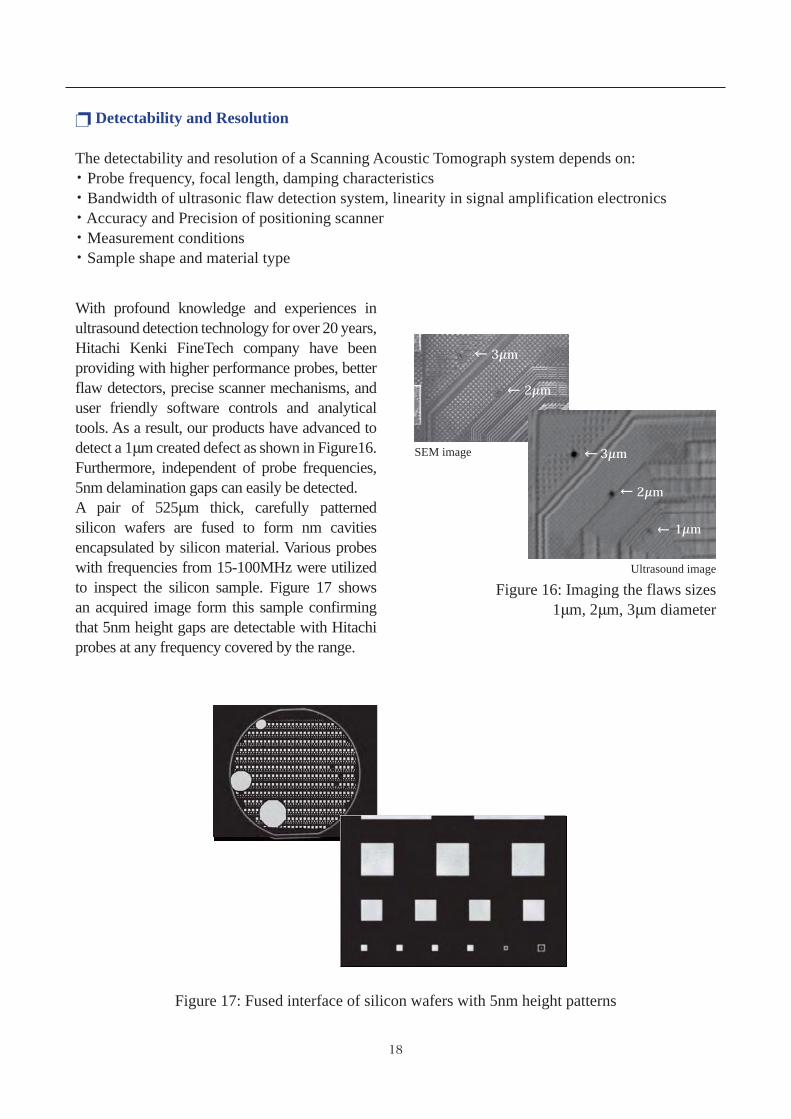
With profound knowledge and experiences in ultrasound detection technology for over 20 years, Hitachi Kenki FineTech company have been providing with higher performance probes, better flaw detectors, precise scanner mechanisms, and user friendly software controls and analytical tools. As a result, our products have advanced to detect a 1μm created defect as shown in Figure16. Furthermore, independent of probe frequencies, 5nm delamination gaps can easily be detected.A pair of 525μm thick, carefully patterned silicon wafers are fused to form nm cavities encapsulated by silicon material. Various probes with frequencies from 15-100MHz were utilized to inspect the silicon sample. Figure 17 shows an acquired image form this sample confirming that 5nm height gaps are detectable with Hitachi probes at any frequency covered by the range.
Figure 17: Fused interface of silicon wafers with 5nm height patterns
Figure 16: Imaging the flaws sizes1μm, 2μm, 3μm diameter
3μm
3μm
2μm
2μm
1μm
SEM image
Ultrasound image
19
λ:Wavelength f:Focal lengthD:Transducer Diameter
Estimation of ultrasonic beam diameter at focal point
Ultrasonic beam diameter at the focal pointd = 0.71λf/(d/2)
D
d
f
Piezo
λ
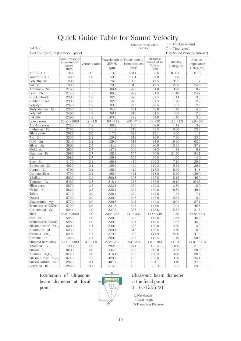
Quick Guide Table for Sound Velocityt=CT/2T=2t/C=2t(mm) /C(km/sec) (μsec)
t = Thickness(mm)T = Time(μsec)C = Sound velocity (km/sec)
Sound velocity( longitudinal waves )(m/s)
Verocity ratioWavelength at 25MHz(μm)
Travel time to 1mm distance(nsec)
Distance travelled in 50nsec(μm)
Density(10kg/m)
Acoustic impedance(10kg/ms)
Air(20℃) 344 0.2 13.8 5814 8.6 0.001 0.00 Water(20℃) 1480 1.0 59.2 1351 37.0 1.00 1.5 Polyethylene 1900 1.3 76.0 1053 47.5 0.92 1.7 Solder 1980 1.3 79.2 1010 49.5 12.60 24.9 Antimony Sb 2160 1.5 86.4 926 54.0 3.80 8.2 Lead Pb 2170 1.5 86.8 922 54.3 11.40 24.7 Vinyl chloride 2300 1.6 92.0 870 57.5 1.44 3.3 Rubber(hard) 2300 1.6 92.0 870 57.5 1.20 2.8 Polystyrol 2340 1.6 93.6 855 58.5 1.05 2.5 Molybdenum Mo 2350 1.6 94.0 851 58.8 1.70 4.0 Polymid 2460 1.7 98.4 813 61.5 1.06 2.6 Bakelite 2590 1.8 103.6 772 64.8 1.40 3.6 Epoxy resin 2500~2800 1.7~1.9 100~112 800~714 63~70 1.15~1.3 2.9~3.6Acrylate resin 2720 1.8 108.8 735 68.0 1.18 3.2 Cadmium Cd 2780 1.9 111.2 719 69.5 8.60 23.9 Silver paste 2925 2.0 117.0 684 73.1 4.00 11.7 Tin Sn 3230 2.2 129.2 619 80.8 7.30 23.6 Gold Au 3240 2.2 129.6 617 81.0 19.30 62.5 Silver Ag 3600 2.4 144.0 556 90.0 10.50 37.8 Mold resin 3930 2.7 157.2 509 98.3 1.72 6.8 Platinum Pt 3960 2.7 158.4 505 99.0 21.40 84.7 Ice 3980 2.7 159.2 503 99.5 1.00 4.0 Zinc Zn 4170 2.8 166.8 480 104.3 7.10 29.6 Zirconium Zr 4650 3.1 186.0 430 116.3 6.44 29.9 Copper Cu 4700 3.2 188.0 426 117.5 8.90 41.8 German silver 4750 3.2 190.0 421 118.8 8.40 39.9 42Alloy 5020 3.4 200.8 398 125.5 8.15 40.9 Tungsten W 5460 3.7 218.4 366 136.5 19.10 104.3 Silica glass 5570 3.8 222.8 359 139.3 2.70 15.0 Nickel Ni 5630 3.8 225.2 355 140.8 8.80 49.5 Teflon 5710 3.9 228.4 350 142.8 1.35 7.7 Quartz 5750 3.9 230.0 348 143.8 2.65 15.2 Magnesium Mg 5770 3.9 230.8 347 144.3 10.00 57.7 Stainless steel(SUS304) 5790 3.9 231.6 345 144.8 7.91 45.8 Germanium Ge 5944 4.0 237.8 336 148.6 5.32 31.6 Steel 5870~5950 4.0 235~238 341~336 147~149 7.80 45.8~46.4Iron Fe 5950 4.0 238.0 336 148.8 7.86 46.8 Stainless steel(SUS405) 5980 4.0 239.2 334 149.5 7.67 45.9 Silicon dioxide SiO2 6000 4.1 240.0 333 150.0 2.20 13.2 Aluminum Al 6260 4.2 250.4 319 156.5 2.70 16.9 Zirconia ZrO2 6994 4.7 279.8 286 174.9 5.90 41.3 Chrome Cr 7020 4.7 280.8 285 175.5 7.19 50.5 Sintered hard alloy 6800~7300 4.6~4.9 272~292 294~274 170~183 11~15 74.8~109.5Titanium Ti 7300 4.9 292.0 274 182.5 3.00 21.9 Silicon Si 8600 5.8 344.0 233 215.0 2.33 20.0 Alumina Al2O3 10410 7.0 416.4 192 260.3 3.80 39.6 Silicon nitride Si3N4 10743 7.3 429.7 186 268.6 3.20 34.4 Silicon carbide SiC 12043 8.1 481.7 166 301.1 3.10 37.3 Berylium Be 12890 8.7 515.6 155 322.3 1.82 23.5
Distance travelled in 50nsec
SAT2-1(E)D080710
http://www.hkft.co.jp
Itopia Yushima Bldg. 19-11 3-chome, Yushima Bunkyo-Ku, Tokyo 113-0034 JapanPhone:+81-3-5688-5428 Fax:+81-3-5688-5429
For more information: