scaling up silicon photonics: where are the challengeseexu/optics2017/wim_imec_optics_2017.pdf · 1...
TRANSCRIPT

1
SCALING UP SILICON PHOTONICS:
WHERE ARE THE CHALLENGES
Wim Bogaerts
OPTICS2017 Workshop, Lausanne, 31 March 2017

2
THE PHOTONICS RESEARCH GROUP
Research Group of Ghent University
— within Engineering Faculty
— within Dept. of Information Technology (INTEC)
— associated with IMEC
— member of NB Photonics
8 Professors (5 ERC grantees)
16 postdocs
50 PhD students
10 support staff
1 Business developer
15 nationalities

3
WHAT IS SILICON PHOTONICS?
The implementation of high density photonic integrated circuits by
means of CMOS process technology in a CMOS fab
Enabling complex optical functionality on a compact chip at low costPictures, courtesy of imec

4
THE PAST 15 YEARS: STUNNING RESEARCH PROGRESS
PUBLICATIONS EACH YEAR
(Conferences not included)
Start of industrialinterest

5
INDUSTRIAL TAKE-UP EXAMPLES IN TELECOM/DATACOM/DATA CENTERS
• active optical cables (eg PSM4: 4x28 Gb/s on parallel fibers)
• WDM transceivers (eg 4 WDM channels x 25 Gb/s on single fiber)
• coherent receiver (eg 100 Gb/s PM-QPSK)
• fiber-to-the-home bidirectional transceiver (eg 12 x 2.5 Gb/s)
• monolithic receiver (eg 16x20Gb/s)
• 40Gb/s, 50Gb/s and 100 Gb/s Ethernet (future: 400Gb/s)
• …

6
WHY SILICON PHOTONICS?
ScaleLarge scale manufacturing
Submicron-scale waveguides

7
WAVEGUIDES: SILICON PHOTONIC WIRES
High index contrast waveguides
• submicrometer dimensions
• small bend radius
• high-density photonics
(> 10000 components/chip)
Si substrate
silicon-oxide
500 nm
200 nm
optical mode
Si
SiO2

8
HIGH INDEX CONTRAST: A BLESSING AND A CURSE
CMOS technology is the only manufacturing technology with sufficient nm-process control to take advantage of the blessing without suffering from the curse
Every nm3 matters
Si
SiO2
[2um box]

9
VARY LARGE SCALE (INTEGRATION)
TSMC Fab 141.4M 300mm wafers / year
Source: TSMC

10
ECONOMY OF (WAFER) SCALE
Wafer-scale economics
— Larger wafers
— Higher volumes
— Massive parallellism
— Minimal marginal cost
4”
1975
6”
1980
200mm
1991
300mm
2001
450mm
201?
— More expensive tools
— Higher volumes
— Larger fixed cost

11
ECONOMY OF (WAFER) SCALE
10K 100K 1M 10M 100M
Number of chips/year
(InP PICs)
0.1
1
10
100
€/m
m2
of
chip
are
a
Chip cost per mm2 in a dedicated, loaded fab.
Strong function of volume
Source: JePPIX Roadmap 2015

12
ECONOMY OF (WAFER) SCALE
Chip cost per mm2 in a dedicated, loaded fab.
100
10K 100K 1M 10M 100M1K
Number of chips/year
MP
W
(InP PICs)
0.1
1
10
€/m
m2
of
chip
are
a
Source: JePPIX Roadmap 2015

13
ECONOMY OF (WAFER) SCALE
Chip cost per mm2 in a dedicated, loaded fab.
100
10K 100K 1M 10M 100M1K
Number of chips/year
MP
W
(InP PICs)
0.1
1
10
€/m
m2
of
chip
are
a
SiP in a dedicated fab
SiP in a shared fab
Source: JePPIX Roadmap 2015

14
A SHARED FAB?
CMOS Fab making both CMOS and silicon photonics
• CapEx for CMOS fabrication fully recovered (= old fab)
• Fab should have some (variable) spare capacity
Technological capabilities required?
• preferably 300mm (better wafers)
• 65-90nm CMOS node
• Upgrade with Germanium epi
• Upgrade with better lithography

15
THE DRIVE FOR SILICON PHOTONICS: OPTICAL INTERCONNECTS
Optical communication has
- higher bandwidth
- lower propagation loss
Optical interconnects are shrinking
• Data center
• Rack-level
• Board-level
• Package level
…

16
WHAT IS HIGH VOLUME?
5×5 mm2 per chip1,250 chips / wafer (200mm)40,000 wafers / month
50 Mchips / month
Saturated 200mm fab

17
WHAT IS HIGH VOLUME?
5×5 mm2 per chip1,250 chips / wafer (200mm)40,000 wafers / month
50 Mchips / month
Saturated 200mm fab 2018
50 mega datacenters10000 racks / center64 cables / rack2 transceivers per cable
64 Mchips
Datacenter Cabling
~1 fabmonth
50 mega datacenters10000 racks / center1000 cables / rack2 transceivers per cable
1 Gchips
Datacenter Cabling
2022
<2 fabyears

18
SILICON PHOTONICS: ONLY FOR INTERCONNECTS?
Transistors: only for calculators?

19
WHEN DOES THIS FUNCTIONALITY/COST MAKE SENSE?
Large Volume
• millions of chips
• high yield
• low cost
High complexity
• thousands of functions on a chip
• large-scale integration
• high cost
• yield?
com
ple
xity
volume

20
BIO & GAS SENSORS
— Silicon photonics: cheap disposable sensor
— Needs transducer to translate the presence of particular
molecules into a refractive index change
— Mostly work on the chemistry / material science side Input grating
coupler50 m
2 m
50 m
2 m
200 m
Fluid channel
Sensor
element
Output grating
Coupler array
9 mm
Input grating
coupler
Input grating
coupler50 m
2 m
50 m
2 m
200 m
Fluid channel
50 m
2 m
50 m
2 m
200 m
50 m
2 m
50 m
2 m
200 m
Fluid channel
Sensor
element
Sensor
element
Output grating
Coupler array
Output grating
Coupler array
9 mmNRC Canada
Genalyte
Genalyte
128 sensorson a chip

21
COMPACT SWITCH MATRICES
32 x 32 switch matrix on a 12 x 12 mm2 chip
Huawei Canada

22
SPECTROSCOPIC SENSOR SYSTEMS
E.g. Integrated glucose monitoring
• 4 spectrometers in 4 wavelength regions
• measure clinically relevant glucose concentrations
in biological fluids
Ugent, IMEC, Indigo Medical

23
LARGE PHASED ARRAYS
Large arrays of optical “antennas”
Individual phase/amplitude control
Beam steering & forming
Jie Sun, MIT, INTEL 2016

24
SILICON PHOTONICS AND CMOS
The STRENGTH of Silicon Photonics
is that it can make use of CMOS-technology
The WEAKNESS of Silicon Photonics
is that it must make use of CMOS-technology
CMOS-technology requires insanely expensive infrastructure but delivers ridiculously cheap chips
with a ludicrous degree of sophistication

25
WHO OWNS A FAB FOR SILICON PHOTONICS?
Vertically integrated electronics manufacturers
• high-end or specialty electronics (e.g. INTEL, ST)
• Silicon Photonics for own use or select partners
CMOS Foundries (TSMC, Global, Silterra, …)
• commodity electronics processes in high volumes
• Silicon photonics for industrial customers
• Need sufficient volume to warrant upfront cost
Research Fabs
• Already running silicon photonics (IMEC, LETI, IME, IHP, CNSE, …)
• Prototyping services and Multi-project-wafer shuttles
• No capacity or interest in larger volumes?

26
TECHNOLOGY PLATFORMS FOR SILICON PHOTONICS
R&D and prototyping platforms:
— Imec, Belgium (MPW-service through ePIXfab / Europractice)
— CEA-LETI, France (MPW-service through Europractice/CMP)
— VTT, Finland (“thick SOI”)
— IME, Singapore (MPW-service)
— AIM-Photonics, USA (MPW service starting 2016)
— AIST (MPW service planned in 2018)
Manufacturing platforms:
— Freescale
— ST Microelectronics
— IBM
— Intel
— GlobalFoundries
— TowerJazz

27
MULTI-PROJECT-WAFER (MPW) SERVICE
The “reticle” (= basic unit that is repetitively patterned on the wafer)
has a maximum size of 25 x 25 mm.
That equals 25 times a 5x5 mm chip.
On a 200 (300) mm wafer you can fit 50 (110) full fields.
So, let’s get organized.
1. Collect 25 5x5 mm designs from different users.
2. Combine these designs on a single mask set
3. Collectively process the wafers
(typically 25 wafers in one batch)
4. Dice the wafers down to 5x5 mm chips (!!)
5. Send a few dozens of 5x5 mm chips to each
user, together with an invoice.

31
FABLESS SILICON PHOTONICS
Many fabless Silicon Photonics companies have emerged
• from direct collaboration with fabs (Luxtera, ...)
• starting from MPW (Caliopa, Genalyte, Acacia)
Established players are also partnering
• e.g. Finisar with ST
• Many keep their fab a secret
How to enter as a new (fabless) startup?

32
SILICON PHOTONICS: FROM IDEA TO PRODUCT
What if you do not have a fab?
Variational validation• MPW in research fabs• multiple samples• develop packaging
Test your idea• prototype in your
own clean room• rapid iteration cycles
Low volume sampling• Dedicated run in
research fab• Allows qualification testing
High volume production• Dedicated run in
volume fab

33
SCALING TO HIGH-VOLUME PRODUCTION
Process transfer from research fab to commercial fab
• match the geometries
• match the performance (including variability)
• match the design kit and models
• migrate the other parts of the supply chain (e.g. assembly)

34
IMEC SILICON PHOTONICS:
FROM R&D PIPELINE TO VOLUME MANUFACTURING
Early Research in imec’s Optical I/O Research Program
Development & Prototyping at imec
— Limited amount of wafers/year
— Reliability qualification ongoing
High-Volume Manufacturing at Commercial Foundry
— imec enables production path at commercial foundry
— 95% of the flow compatible with CMOS90 technology

35
FROM SAMPLING TO LOW-VOLUME PRODUCTION
Most Research Fabs (MEC, LETI, IME) offer a LVM model
Low volume (< 1000 wafers / year) can already be enough for first market
Low technology threshold
Potentially high financial threshold (research fabs are expensive per chip)
Potentially long production cycles
36
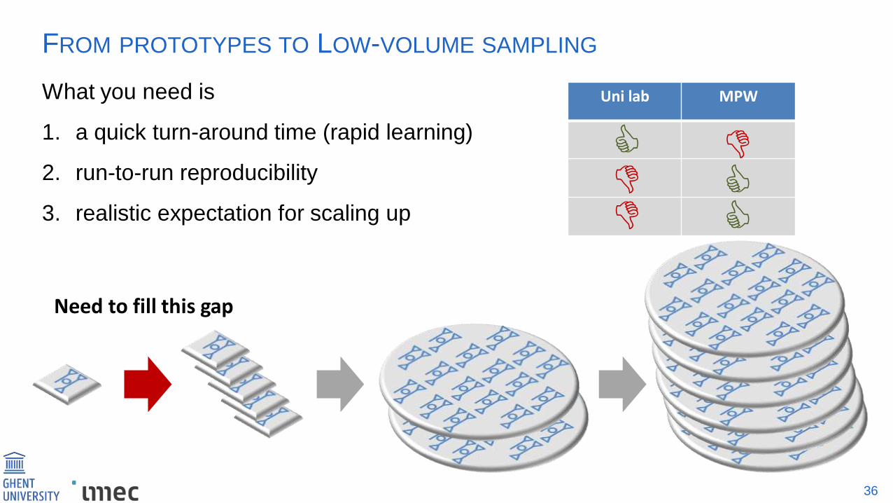
FROM PROTOTYPES TO LOW-VOLUME SAMPLING
What you need is
1. a quick turn-around time (rapid learning)
2. run-to-run reproducibility
3. realistic expectation for scaling up
Uni lab MPW
Need to fill this gap

37
FROM PROTOTYPES TO LOW-VOLUME SAMPLING
Fast prototyping fabs, compatible with MPW fabs
• Fast (days or weeks instead of months)
• Very low volume (1-10 chips)
• Calibrated against an MPW fab
• Similar processes and specs
• Similar design flow and design rules
• Consistent quality (monitored process)
• Supported by PDK with models and statistics
• At a similar cost per run

38
SIP PROTOTYPING SERVICES ARE EMERGING
IPH, AMO (Germany)
Australia Silicon Photonics
ORC in Southampton (UK)
KIT (Germany)
UBC / UWashington (Canada/US)
Applied NT (Canada)

39
YOU NEED MORE THAN JUST A FAB
• Design and simulation tools (and services): the supply chain is developing
• Packaging tools: rapid progress but still a long way to go
New H2020 PIC-packaging project will develop the supply chain

40
PIC PACKAGING @ TYNDALL

41
WHEN DOES THIS FUNCTIONALITY/COST MAKE SENSE?
Large Volume
• millions of chips
• high yield
• low cost
High complexity
• thousands of functions on a chip
• large-scale integration
• high cost
• yield?
com
ple
xity
volume

42
COMPONENTS PER CHIP
“Moore’s law for Silicon Photonics”
A. Khanna et al. OFC2017, Th1B.3

43
CONNECTIVITY BEGETS COMPLEXITY BEGETS FUNCTIONALITY
Integrated Electronics
• billions of digital gates: unprecedented logic performance
• millions of analog transistors: unprecedented control
(even with imperfect components: enabled by design!)
Integrated Photonics (in Silicon)
• technological potential of 10000+ photonic elements on a chip
• not even scratched the surface of what this could do
Needs design and control
Moreelements
Morecomplexity
Morefunctionality

44
SCALING COMPLEXITY
Many components on a chip
Scalable building blocks
• connectivity
• cascadability
• variability
Design scaling
• synthesis tools
• accurate models
• yield prediction
Operational scaling
• control and feedback 10000s optical elements
100s opticalIOs
10s RF IOs
1000s electrical control IOs
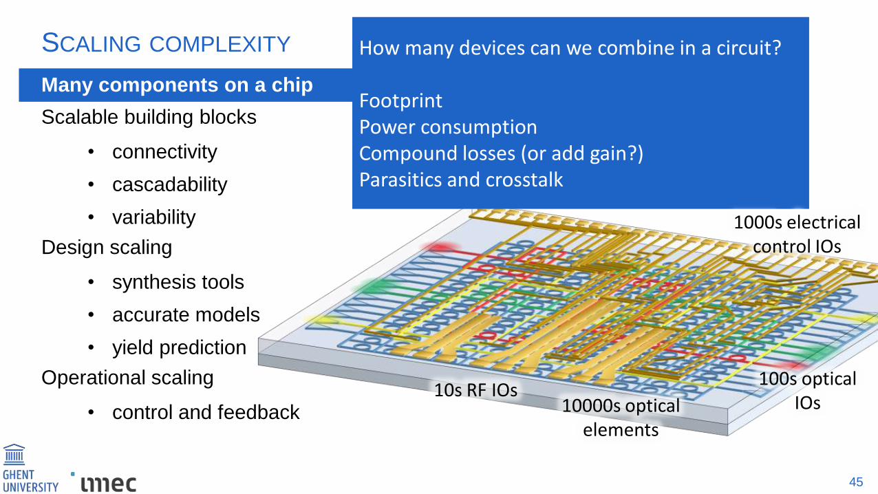
45
SCALING COMPLEXITY
Many components on a chip
Scalable building blocks
• connectivity
• cascadability
• variability
Design scaling
• synthesis tools
• accurate models
• yield prediction
Operational scaling
• control and feedback 10000s optical elements
100s opticalIOs
10s RF IOs
How many devices can we combine in a circuit?
FootprintPower consumptionCompound losses (or add gain?)Parasitics and crosstalk
1000s electrical control IOs

46
LOWER LOSSES.
Better technology
• 300mm wafers and tools give
better performance
• immersion lithography gives
better linewidth control
• lower sidewall roughtness
reduces loss and backreflection
Other geometries and materials
• rib waveguides
• SiN waveguides

47
LOSS COMPENSATION
Introduce Gain in silicon photonics
• III-V semiconductors
• Bonding
• Epitaxy
• Germanium
• Erbium-doped waveguide amplifiers
• Parametric gain (4-wave mixing)
Silicon waveguide
Buried oxide
III-V wafer
SiO2SiO2
DVS-BCB

57
MODULATORS CONSUME A LOT OF SPACE
Not really in line with ‘submicron’ Silicon Photonics
Alternative phase modulators,
tuners and switches?
Electro-optic Modulators
Everything else
L-PIC CWDM4 Tx

58
EFFECT MAGNITUDE VS. SPEED
Pockels (2) (fs)
Polymers, perovskites
Mag
nit
ud
e o
f th
e ef
fect
Speed of the effect
Thermal (us)
Heaters
Carriers (ns)
Diodes, capacitors
Birefrigence (ms)
Liquid crystals
Tuning
Switching
Modulation
Mechanical (ms-us)
MEMS, NEMS

59
ALTERNATIVE MODULATOR AND SWITCH TECHNOLOGIES
Modulators
Electro-Optic Polymers in Slot Waveguides
— Very good performance, but ready as a platform?
Ferro-Electrics on Silicon
— Pure phase modulation
— difficult material integration
— Recent breakthroughs in loss
Germanium-EA Absorbers
— Direct intensity modulation, but no phase modulation
— High speed, low power demonstrated
Graphene on Silicon
— Direct intensity modulation
— Much work needed
Switches
Large-Scale MEMS Fabrics
— Up to 50x50 switch matrices demonstrated
— Large bandwidth and high XT
Liquid Controlled Adiabatic Switches
— Towards no static power consumption
— Broadband low loss operation
Liquid Crystal based switches

60
PHOTONICS IS JUST ONE PART OF THE SYSTEM
Large-scale photonics requires integrated electronics
• Logic
• Control
photonics
analogelectronics
digitalelectronics
software user

61
INTEGRATION WITH ELECTRONICS: SCALING
Photonics interfaced with electronics
• Monolithic
• Low parasitics. all-in-one process.
• Not the optimal process for either.
• Feature size mismatch
• Flip-chip
• Large bond-pads, density limited
• Parasitics
• 3D stacking
• Best process for both
• Co-design and yield?
IBM
IMEC

62
SCALING COMPLEXITY
Many components on a chip
Scalable building blocks
• connectivity
• cascadability
• variability
Design scaling
• synthesis tools
• accurate models
• yield prediction
Operational scaling
• control and feedback
Automating designpredict the behavior (statistical)First-time right design

63
DESIGNING PHOTONIC INTEGRATED CIRCUITS
Can we learn from electronic ICs?
• Millions of analog transistors
• Billions of digital transistors
• Power, timing and yield
• First time right designs
• Very mature Electronic Design Automation (EDA) tools!
• A well established design flow
Does this apply to photonics?

66
DESIGN ENVIRONMENTS ARE EMERGING
Combinations of Photonics Design and EDA
Physical simulation combined with circuit design
Physical and functional verification
First PDKs with basic models

67
COMPONENT DESIGN VS. CIRCUIT DESIGN
10 years ago: Component Design Now also: Circuit design
layout
geometry
simulation
Circuitcapture
simulation
layout

68
PHOTONIC+ELECTRONIC CIRCUIT SIMULATION
Photonics does not fit in Spice
Effort-flow systems
Photonics used other formalisms (more like RF waves)
Electrical Voltage Current
Fluidic Pressure Flow
Thermal Temperature Heat Flow*
Mechanical Force Motion
Photonic? - -

69
SIGNALS IN A PHOTONIC CIRCUIT
How much information needs to be exchanged per time step?
• phase?
• spectral information?
• multimode waveguides?
• unidirectional or bidirectional?
3dB
lasermodul
atordetector
detector

70
SIGNAL REPRESENTATION: EFFECTS CAN BE MODELED
Accuracy
Amount of information needed
Power
PowerPhase
PowerPhase
WavelengthMode
PowerPhase
WavelengthMode
N channels
PowerPhase
Spectrum
interferometry
propagation loss
phase modulation
channel crosstalk
chirp, slow nonlinearities

71
links with resonant devices
SIGNAL REPRESENTATION: APPLICATION DESIGN
Accuracy
Amount of information needed
Power
PowerPhase
PowerPhase
WavelengthMode
PowerPhase
WavelengthMode
PowerPhase
N channels
Spectrum
point-to-point links
coherent links
simpleWDM links
Spectrometers

72
INTEGRATE PHOTONIC AND ELECTRONIC CIRCUIT SIMULATION
Photonics = Optics + Electronics.
We need to combine the two in the design process.
• Verilog A: Represent Optical Signals
as ‘Voltages’ or ‘Power’
• Use busses for power, phase
(real/imag) and wavelength
• Cosimulation with Photonic
Circuit simulator laserwaveguide
photodiode
Vin Vout
electrical transmitter electrical receiver
optical link
TIA

73
PHOTONICS IN VERILOGA
Encode time signals as ‘analytical’ signals
(complex numbers)
Bus of two lines for bidirectionality
Modulation on an optical wavelength
C. Sorace-Agaskar, OpEx 23(21), 2015

74
PHOTONIC-ELECTRONIC COSIMULATION
Full separation possible?
• In some cases (e.g. link)
• simulation in one direction
• exchange waveforms
• No feedback!
laserwavegui
dephotodio
de
Vin Vout
electrical transmitter electrical receiver
optical link
TIA

75
FUTURE: MIXED-SIGNAL CO-SIMULATION
2 or more simulators:
• data exchange
• synchronization
• common netlist
• data readout
• …
laserwavegui
dephotodio
de
Vin Vout
electrical transmitter electrical receiver
optical link
TIA

76
CO-SIMULATION
Optical and electrical co-design in Virtuoso Schematic
Photonic simulation in Lumerical Interconnect
A. Farsaei, APC 2016, JTu4A.1

77
VARIABILITY: PREDICTING CIRCUIT YIELD

78
VARIABILITY ≠ VARIABILITY
Wafer – to – wafer variability
Die – to – die variability
Intra-die variability
- mask-related
- distance related
- stochastic
Thickness map
linewidth map

79
Device error
• Fabrication
• Operation
Monte-Carlo
• Simulation
• Measurement
• Expensive
Statistics
• Standard deviation
• Probability density
• Yield prediction
DEVICE VARIABILITY ANALYSIS
Standard technique: Monte-Carlo simulations
Requires many expensive simulations
Y. Xing, Photon. Res. 2016

80
Device error
• Fabrication
• Operation
Stochastic model
• Limited number of Simulation or Measurement
Monte-Carlo
• With stochastic model of the device (analytical functions)
Statistics
• Standard deviation
• Probability density
• Yield prediction
DEVICE VARIABILITY ANALYSIS
Build stochastic model from small set of simulations
Use Monte-Carlo on Stochastic model

81
Technique Mean value of field coupling Standard Deviation of
field couplingComputational
timeMC via
Fimmwave65229.29 2716.5 22h 1min
SC modelling + MC via SC
65236.43 2720.04 9 min 50.52 s
DEVICE VARIABILITY ANALYSIS WITH STOCHASTIC COLLOCATION
• Sampling-based interpolation modelling technique
• Random variables with arbitrary distribution
• Example: variability of directional coupler
Y. Xing, Photon. Res. 2016

82
1000s electronicfeedback loops
SCALING COMPLEXITY
Many components on a chip
Scalable building blocks
• connectivity
• cascadability
• variability
Design scaling
• synthesis tools
• accurate models
• yield prediction
Operational scaling
• control and feedback
Even with today’s technology:Perfection is achievable
10000s optical elements
100s opticalIOs
10s RF IOs
1000s electrical control IOs

83
MAKING PERFECT OPTICS WITH IMPERFECT COMPONENTS
Replace specialty optical component with a more complex circuit
• Simple building blocks
• (Many) tunable elements
• Simple feedback loops
e.g. Linear N×N circuit
• tunable 2×2 couplers
• tunable delay lines
• monitor detectorsD.A.B. Miller, Optica 2, 747-750 (2015)
84
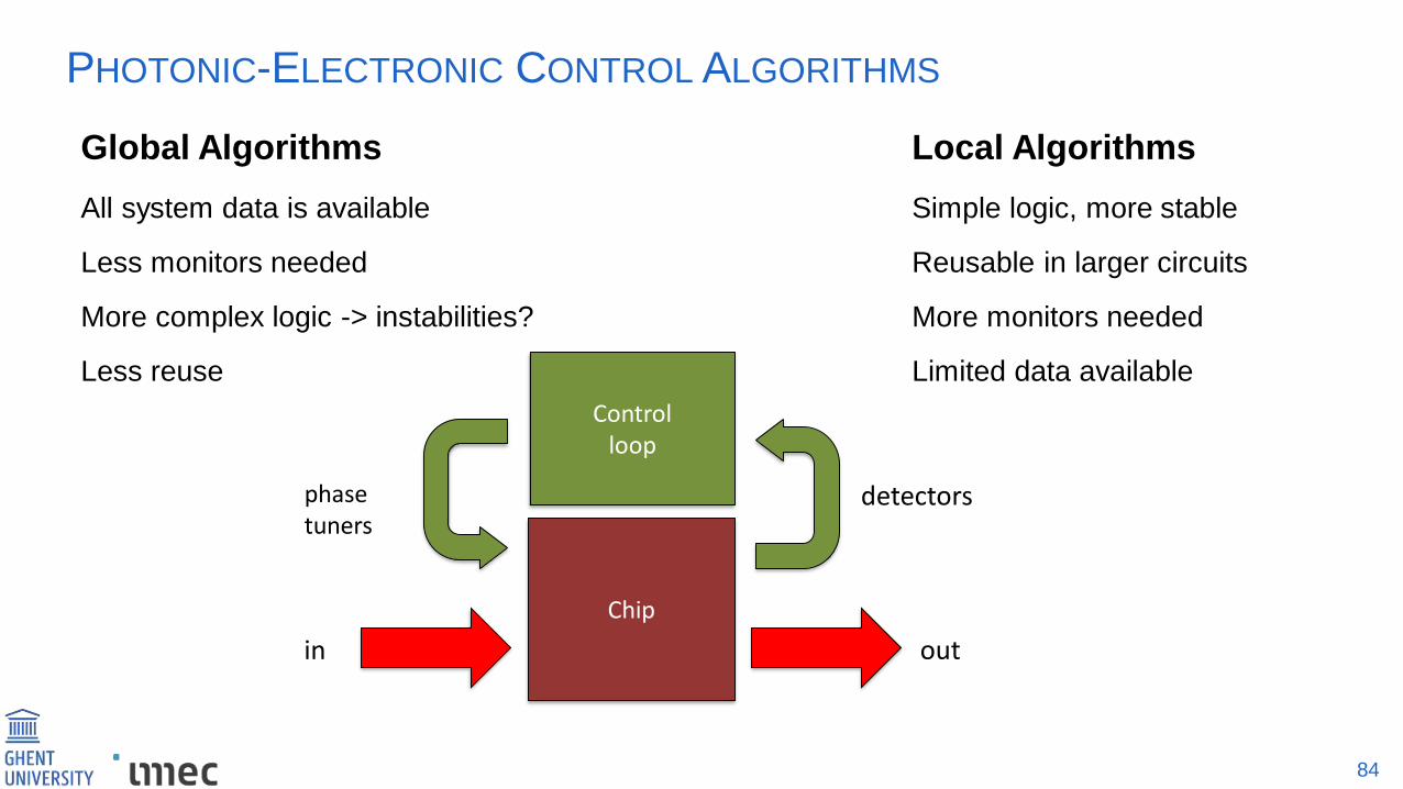
PHOTONIC-ELECTRONIC CONTROL ALGORITHMS
Global Algorithms
All system data is available
Less monitors needed
More complex logic -> instabilities?
Less reuse
Local Algorithms
Simple logic, more stable
Reusable in larger circuits
More monitors needed
Limited data available
Chip
Controlloop
detectors
in out
phase tuners

85
UNIVERSAL LINEAR CIRCUIT IN SILICON
Beam splitters = MZI
Phase shifters: Simple Heaters
Power monitors:Directional coupler tapIO channels:
grating couplers
Ribeiro et al, Optica 2016

86
ADAPTIVE BEAM COUPLER
Circuit adapts itself to maximize
output to a single mode waveguide
Local feedback loops stabilize
the entire circuit.
Feedback on
Feedback off
Temperature
Ribeiro et al, Optica 2016

87
MORE THAN JUST PHOTONS
Silicon photonics goes beyond the optical chip
100s optical IOs
1000s electronicfeedback loops
10s RF signals
software configuration
1000s electrical IOs
10000s optical elements

88
PHOTONICS IS JUST ONE PART OF THE SYSTEM
photonics
analogelectronics
digitalelectronics
software user
Just good enough photonics technologyFairly simple silicon photonic circuits (e.g. simple transceiver)Electronics and software is added to make a systemExisting electronic techniques are used to compensate for photonics

89
SUMMARY
Economic Scaling in Silicon Photonics
• Based on CMOS fabrication models.
• Large volumes or uniquely large value (complexity)
• New routes emerging for R&D
The only technology to allow complexity scaling
(circuit density and connectivity)
Process technology is ‘good enough’ today, but
• Complexity scaling is limited by the design process
• Complexity scaling is limited by the control logic

90
SILICON PHOTONICS DESIGN COURSE
Gain a deep understanding of the design flow for silicon photonics
— circuit design and simulation
— component design and simulation
— parametric mask layout and verification
You will design a small chip that will
be actually fabricated and characterized
Ghent University
— 19-23 June
— 4-5 September
idea/concept
designlayout
simulatefunction
designfunction
checkdesignrules
verifydesign
function
fabricatedevice
test
Back-EndFront-End

91
MPW Fabs
BrokersProto-Fabs
Design software
Packaging
Societies
Design houses
THE ECOSYSTEM
Volume Fabs

92
@PhotonicsUGent
www.photonics.intec.ugent.be
E
T
Wim Bogaerts
Professor in Silicon Photonics
+32 9 264 3324