scad engineering college - scadec.ac.inscadec.ac.in/upload/file/rf_notes.pdf · ec2403 rf and...
TRANSCRIPT

SCAD Engineering College
EC2403 RF AND MICROWAVE ENGINEERING
UNIT I
INTRODUCTION:
Apparatus and techniques may be described qualitatively as "microwave" when the wavelengths of signals are roughly the same as the dimensions of the equi ment, so that lumped-element circuit theory
is inaccurate. As a consequence, practical microwave technique tends to move away from the discrete resistors, capacitors, and inductors used with lower freq ency radio waves. Instead, distributed circuit
elements and transmission-line theory are more sef l methods for design, analysis. Open-wire and coaxial transmission lines give way to waveg ides, and l mped-element tuned circuits are replaced by cavity resonators or resonant lines. Effects of reflection, polarization, scattering, diffraction, and atmospheric absorption usually ssoci ted with visible light are of practical significance in the study of microwave propagation. The s me equ tions of electromagnetic theory apply at all frequencies.
terahertz radiation, micro aves, and ultra-high-frequency radio waves are fairly arbitrary and are used
variouslybeteendifferentfields of study. The term microwave generally refers to "alternating current
signals with frequencies bet een 300 MHz (3×10⁸ Hz) and 300 GHz (3×10
11 Hz)."
[1] Both IEC standard
60050 and IEEE standard 100 define "microwave" frequencies starting at 1 GHz (30 cm wavelength).
Electromagnetic aves longer (lower frequency) than microwaves are called "radio waves". Electromagnetic radiation with shorter wavelengths may be called "millimeter waves", terahertz radiation or even T-rays. Definitions differ for millimeter wave band, which the IEEE defines as 110 GHz to 300 GHz.
Discovery
The existence of electromagnetic waves, of which microwaves are part of the frequency spectrum, was
predicted by James Clerk Maxwell in 1864 from his equations. In 1888, Heinrich Hertz was the first to
demonstrate the existence of electromagnetic waves by building an apparatus that produced and
detected microwaves in the UHF region. The design necessarily used horse-and-buggy materials,
including a horse trough, a wrought iron point spark, Leyden jars, and a length of zinc gutter whose
parabolic cross-section worked as a reflection antenna. In 1894 J. C. Bose publicly demonstrated radio
control of a bell using millimetre wavelengths, and conducted research into the propagation of
microwaves.
Plot of the zenith atmospheric transmission on the summit of Mauna Kea throughout the entire gigahertz range of the electromagnetic spectrum at a precipitable water vapor level of 0.001 mm. (simulated)
Frequency range

SCAD Engineering College
Above 300 GHz, the absorption ofelectromagneticradiationbyEarh'samophreiso great that it is
effectively opaque, until the atmosphere becomes transparent again in he so-call d infrared and optical The microwave range includes ultra-high frequency (UHF) (0.3–3 GHz), uper high frequen y (SHF)
(3–30 GHz), and extremely high frequency (EHF) (30–300 GHz) signals.
Microwave Sources
Vacuum tube based devices operate on the ballistic motion of electrons in a vacuum under the influence of controlling electric or magnetic fields, and include the magnetron, klystron, travelling wave tube (TWT), and gyrotron. These devices work in the density modulated mode, rather than the current modulated mode. This means that they work on the basis of clumps of electrons flying ballistically through them, rather than using a contin o s stream. A maser is a device similar to l ser, except that it works at microwave frequencies. Solid-state sources include the . field-effect tr nsistor, at least at lower frequencies, tunnel diodes and Gunn Uses
Communication
Before the advent of fiber optic transmission, most long distance telephone calls were carried via
microwave point-to-point links through sites like the AT&T Long Lines. Starting in the early 1950's, frequency division multiplex was used to send up to 5,400 telephone channels on each microwave radio channel, with as many as ten radio channels combined into one antenna for the hop to the next site, up to 70 km away.
Wireless LAN protocols, such as Bluetooth and the IEEE 802.11 specifications, also use
microwaves in the 2.4 GHz ISM band, although 802.11a uses ISM band and U-NII frequencies in the 5 GHz range. Licensed long-range (up to about 25 km) Wireless Internet Access services can be found in many countries (but not the USA) in the 3.5–4.0 GHz range.
Metropolitan Area Networks: MAN protocols, such as WiMAX (Worldwide Interoperability for
Microwave Access) based in the IEEE 802.16 specification. The IEEE 802.16 specification was
designed to operate between 2 to 11 GHz. The commercial implementations are in the 2.3GHz, 2.5 GHz, 3.5 GHz and 5.8 GHz ranges.
Wide Area Mobile Broadband Wireless Access: MBWA protocols based on standards
specifications such as IEEE 802.20 or ATIS/ANSI HC-SDMA (e.g. iBurst) are designed to
operate between 1.6 and 2.3 GHz to give mobility and in-building penetration hara teristics
similar to mobile phones but with vastly greater spectral efficiency.
Cable TV and Internet access on coaxial cable as well as broadcast televi ion u e some of the
. com

SCAD Engineering College
lower microwave frequencies. Some mobile phone networks, like GSM, al o u e the lower microwave frequencies.
Microwave radio is used in broadcasting and telecommunic ion r nsmissions because, due to
their short wavelength, highly directive antennas are sm ller nd therefore more practical than
they would be at longer wavelengths (lower frequencies). There is lso more bandwidth in the
microwave spectrum than in the rest of the radio spectrum; the usable bandwidth below 300 MHz is less than 300 MHz while many GHz can be used above 300 MHz. Typically,
microwaves are used in television news to transmit a signal from a remote location to a television station from a specially equipped van.
Remote Sensing
Radar uses microwave r di tion to detect the range, speed, and other characteristics of remote
objects. Development of r d r w s ccelerated during World War II due to its great military utility. Now radar is widely used for pplications such as air traffic control, navigation of ships,
and speed limit enforcement
. A Gunn diode oscillator and waveguide are used as a motion detector for automatic door
openers (although these are being replaced by ultrasonic devices).
Most radio astronomy uses microwaves. Micro ave imaging; see Photoacoustic imaging in biomedicine
Navigation
Global Navigation Satellite Systems (GNSS) including the American Global Positioning System (GPS) and the Russian ГЛОбальная НАвигационная Спутниковая Система (GLONASS) broadcast navigational signals in various bands between about 1.2 GHz and 1.6 GHz.
CAD Engineering College Power
A microwave oven passes (non-ionizing) microwave radiation (at a frequency near 2.45 GHz) through food, causing dielectric heating by absorption of energy in the water, fats and
sugar contained in the food. Microwave ovens became common kitchen appliances in Western countries in the late 1970s, following development of inexpensive cavity
magnetrons. Microwave heating is used in industrial processes for drying and curing products. Many semiconductor processing techniques use microwaves to generate plasma f r such
purposes as reactive ion etching and plasma-enhanced chemical vapor deposition (PECVD). Microwaves can be used to transmit power over long distances, and post- . World War II research
Less-than-lethal weaponry exists that uses millimeter waves o h at a hin layer of human skin to
SCAD Engineering College
an intolerable temperature so as to make the targeted person move away. A two-second burst of the 95 GHz focused beam heats the skin to a temper ture of 130 F (54 C) at a depth of 1/64th of an inch (0.4 mm). The United States Air Force and M rines re currently using this type of Active Denial System.
[2]
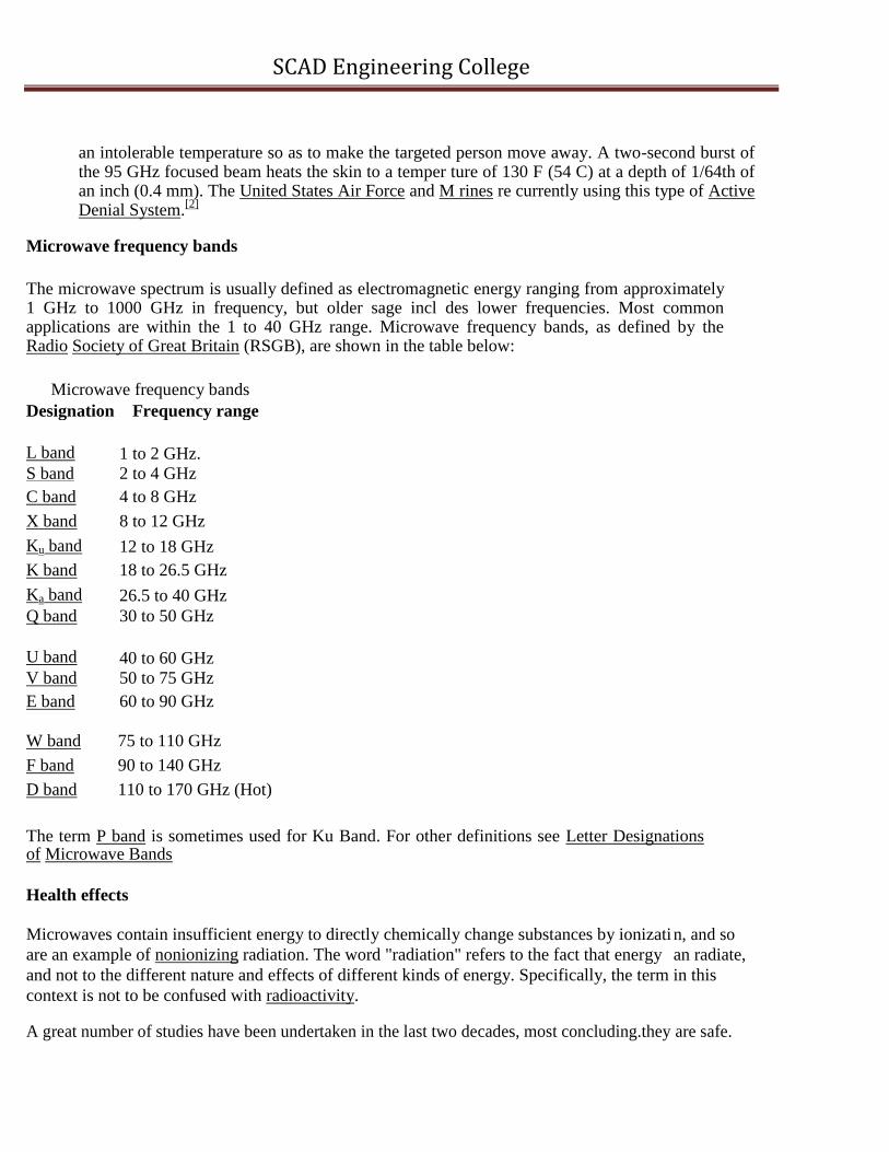
Microwave frequency bands
The microwave spectrum is usually defined as electromagnetic energy ranging from approximately 1 GHz to 1000 GHz in frequency, but older sage incl des lower frequencies. Most common applications are within the 1 to 40 GHz range. Microwave frequency bands, as defined by the Radio Society of Great Britain (RSGB), are shown in the table below:
Microwave frequency bands
Designation Frequency range
L band
1 to 2 GHz.
S band 2 to 4 GHz
C band 4 to 8 GHz
X band 8 to 12 GHz
Ku band 12 to 18 GHz
K band 18 to 26.5 GHz
Ka band 26.5 to 40 GHz
Q band 30 to 50 GHz
U band
40 to 60 GHz
V band 50 to 75 GHz
E band 60 to 90 GHz
W band 75 to 110 GHz F band 90 to 140 GHz D band 110 to 170 GHz (Hot)
The term P band is sometimes used for Ku Band. For other definitions see Letter Designations of Microwave Bands
Health effects Microwaves contain insufficient energy to directly chemically change substances by ionizati n, and so
are an example of nonionizing radiation. The word "radiation" refers to the fact that energy an radiate,
and not to the different nature and effects of different kinds of energy. Specifically, the term in this
context is not to be confused with radioactivity.
A great number of studies have been undertaken in the last two decades, most concluding.they are safe.
SCAD Engineering College
com It is understood that microwave radiation at a level that causes heating of living ti ue is hazardous (due
Perhaps the first use of the word.microwveinanastronomicalcontextoccurredin1946 in an article
"Microwave Radiation from the Sun nd Moon" by Robert Dicke and Robert Beringer. to the possibility of overheating and burns) and most countries have s andards limiting exposure, such as the Federal Communications Commission RF safety regulations.
Synthetic reviews of literature indicate the predominance of their s fety of use.
History and research Perhaps the first, documented, formal use of the term microwave occurred in 1931:
"When trials with wavelengths as low as 18 cm were made known, there was undisguised surprise that the problem of the micro-wave had been solved so soon." Telegraph & Telephone Journal XVII. 179/1
Scattering parameters
"Scattering"isanideatakenfrom billiards, or pool. One takes a cue ball and fires it up the table at a
collection of other balls. After the impact, the energy and momentum in the cue ball is divided
between all the balls involved in the impact. The cue ball "scatters" the stationary target balls and in
turn is deflected or "scattered" by them.
In a microwave circuit, the equivalent to the energy and momentum of the cue ball is the amplitude and
phase of the incoming wave on a transmission line. (A rather loose analogy, this). This incoming wave is "scattered" by the circuit and its energy is partitioned between all the possible outgoing waves on all
the other transmission lines connected to the circuit. The scattering parameters are fixed properties of the
(linear) circuit which describe how the energy couples between each pair of ports or transmission lines connected to the circuit.
Formally, s-parameters can be defined for any collection of linear electronic components, whether or
not the wave view of the power flow in the circuit is necessary. They are algebraically related to the
impedance parameters (z-parameters), also to the admittance parameters (y-parameters) and to a
notional characteristic impedance of the transmission lines.
An n-port microwave network has n arms into which power can be f d and from which power can be A visual demonstration of the meaning of scattering may be given by throwing a piece of chalk at a blackboard....

SCAD Engineering College
Definitions.
.
taken. In general, power can get from any arm (as input) to any o her arm (as output). There are thus n incoming waves and n outgoing waves. We also observe that power can be r fl ct d by a port, so the input power to a single port can partition between all the ports of he n work o form outgoing waves.
Associated with each port is the notion of a "reference plane" t which the wave amplitude and phase is defined. Usually the reference plane associated with a certain port is t the same place with respect to incoming and outgoing waves.
The n incoming wave complex amplitudes are usually designated by the n complex quantities an, and the n outgoing wave complex quantities are designated by the n complex quantities bn. The incoming wave quantities are assembled into an n-vector A and the outgoing wave quantities into an n-vector B. The outgoing waves are expressed in terms of the incoming waves by the matrix equation B = SA where S is an n by n square matrix of complex n mbers called the "scattering matrix". It completely determines the behaviour of the network. In gener l, the elements of this matrix, which are termed "s-parameters", are all frequency-dependent
For example, the matrix equations for a 2-port are
.
b1 = s11 a1 + s12 a2
b2 = s21 a1 + s22 a2
And the matrix equations for a 3-port are
b1 = s11 a1 + s12 a2 + s13 a3
b2 = s21 a1 + s22 a2 + s23 a3
b3 = s31 a1 + s32 a2 + s33 a3 The wave amplitudes an and bn are obtained from the port current and voltages by the relations a = (V + ZoI)/(2 sqrt(2Zo)) and b = (V - ZoI)/(2 sqrt(2Zo)). Here, a refers to an if V is Vn and I In for the nth port. Note the sqrt(2) reduces the peak value to an rms value, and the sqrt(Zo) makes the amplitude normalised with respect to power, so that the incoming power = aa* and the outgoing power is bb*.
SCAD Engineering College
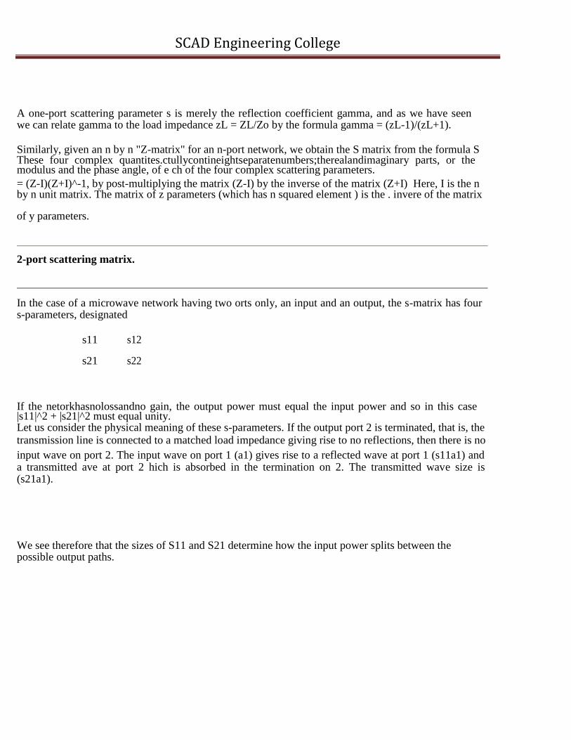
A one-port scattering parameter s is merely the reflection coefficient gamma, and as we have seen we can relate gamma to the load impedance zL = ZL/Zo by the formula gamma = (zL-1)/(zL+1). Similarly, given an n by n "Z-matrix" for an n-port network, we obtain the S matrix from the formula S These four complex quantites.ctullycontineightseparatenumbers;therealandimaginary parts, or the modulus and the phase angle, of e ch of the four complex scattering parameters. = (Z-I)(Z+I)^-1, by post-multiplying the matrix (Z-I) by the inverse of the matrix (Z+I) Here, I is the n by n unit matrix. The matrix of z parameters (which has n squared element ) is the . invere of the matrix of y parameters. 2-port scattering matrix. In the case of a microwave network having two orts only, an input and an output, the s-matrix has four s-parameters, designated
s11 s12
s21 s22
If the netorkhasnolossandno gain, the output power must equal the input power and so in this case |s11|^2 + |s21|^2 must equal unity. Let us consider the physical meaning of these s-parameters. If the output port 2 is terminated, that is, the transmission line is connected to a matched load impedance giving rise to no reflections, then there is no input wave on port 2. The input wave on port 1 (a1) gives rise to a reflected wave at port 1 (s11a1) and a transmitted ave at port 2 hich is absorbed in the termination on 2. The transmitted wave size is (s21a1).
We see therefore that the sizes of S11 and S21 determine how the input power splits between the possible output paths.
SCAD Engineering College
NOTE s21 relates power OUT of 2 to power IN to 1, not vice versa as it is easy to think at first sight.
Clearly, if our 2-port microwave network represents a good amplifier, we need s11 rather small and s21 quite big, let us say 10 for a 20dB amplifier. In general, the s-parameters tell us how much power "comes back" or "comes out" when we "throw
power at" a network. They also contain phase shift information.
Reciprocity
Reciprocity has to do
with the symmetryofthes-matrix.Areciprocals-matrixhasymmetry about the
leading diagonal. Many networks are reciprocal. In the case of a 2-port n twork, that means that s21 = s12 and interchanging the input and output ports does not change he ransmi ion properties. A transmission line section is an example of a reciprocal 2-port. A dual dir c ional coupler is an example of a reciprocal 4-port. In general for a reciprocal n-port sij = sji.
Amplifiers are non-reciprocal; they have to be, otherwise they would be unstable. Ferrite devices are deliberately non-reciprocal; they are used to construct isolators, ph se shifters, circulators, and power combiners.
Examples of scattering matrices.
This is a matrix consisting of.singleelement, the scattering parameter or reflection coefficient. You may thinkofitasa1by1matrix; one row nd one column.
A matched transmission line, s11 = 0 A short circuit, at the short, s11 = 1 angle -180 degrees The input to a 0.2 lambda line feeding a short cicuit, s11 = 1 angle -324 degrees Your turn. A normalised load 2+j1? Your turn again. The input to a transmission line of length 20.35 lambda connected to a normalised load 2+j1?
Two port S-matrices These are 2 by 2 matrices having the following s parameters; s11 s12 s21 s22.
One-port S-matrix

SCAD Engineering College
A 0.1 lambda length of transmission line

SCAD Engineering College
s11 = 0 s12 = 1 angle -36 degrees s21 = 1 angle -36 s22 = 0 A 10dB amplifier, matched on input and ouput ports s11 = 0 s12 = small
s21 = 3.16 angle -theta s22 = 0 An isolator having 1dB forward loss, 21 dB backward loss, matched on ports 1 and 2 s11 = 0 s12 = 0.0891 some angle
s21 = 0.891 some angle s22 = 0
Your turn. A 9 cm length of waveguide of cross sectional dimensions 2.5 cms by 1.8 c s at a
frequency of 8GHz
Your turn again. The waveguide above has a capacitative iris placed mid way al ng it. Assume
that 30% of the power incident on the iris gets through it, and 70% is reflected Hint represent
the normalised load admittance of the iris as y = 1 + js and calculate s for 70% power reflection.
That will give you the phase shift on reflection as well.
.
Three port S-matrices
com
These are 3 by 3 matrices having the following s parameters
s11 s12 s13
s21 s22 s23
s31 s32 s33 Your turn. Write down the s matrix for a perfect circulator with -70 degrees of phase shifts between successive ports. Your turn again. A coaxial cable is connected in a Y arrangement with each arm 12.3 wavelengths long. At the junction, the cable arms are all connected in arallel. Write down its S matrix and comment on this method of splitting power from a TV down lead to serve two television sets.
. If a 1-portnetworkhasreflection gain, its s-parameter has size or modulus greater than unity. More Stability. power is reflected than is incident. The power usually comes from a dc power supply; Gunn diodes can be used as amplifiers in combination with circulators which separate the incoming and outgoing waves. Suppose the reflection gain from our 1-port is s11, having modulus bigger than unity. If the 1-port is connected to a transmission line with a load impedance having reflection coefficient g1, then oscillations may ell occur if g1s11 is bigger than unity. The round trip gain must be unity or greater at an integer number of (2 pi) radians phase shift along the path. This is called the "Barkhausen criterion" for oscillations. Clearly if we have a Gunn source matched to a matched transmission line, no oscillations will occur because g1 will be zero.
If an amplifier has either s11 or s22 greater than unity then it is quite likely to oscillate or go unstable for some values of source or load impedance. If an amplifier (large s21) has s12 which is not negligibly small, and if the output and input are mismatched, round trip gain may be greater than unity giving rise

SCAD Engineering College
to oscillation. If the input line has a
generator mismatch with reflection
coefficient g1, and the load impedance
on port 2 is
mismatched with reflection
coefficient g2, potential instability happens if g1g2s12s21 is greater than unity.
Applications of rat-race couplers are numerous, and include mixers and phase shifters. The
rat-race gets its name from its circular shape, shown below. The circumference is 1 5 wavelengths. For an equal-split rat-race coupler, the impedance of the entire ring is fixed at 1.41xZ0, or 70 7 ohms for a 50
ohm system. For an input signal V , the outputs at ports 2 and 4 (thanks, Tom!) are equal in magnitude,
in .
but 180 degrees out of phase.
com
Microwave Hybrid Circuits, Waveguide Tees, Magic Tees (Hybrid Trees)
HYBRID RINGS (RAT-RACE CIRCUITS)

SCAD Engineering College
.
Rat-race coupler (equal power split) The couplingofthetoarmsis shown in the figure below, for an ideal rat-race coupler centered at 10 GHz (10,000 MHz). An equal power split of 3 dB occurs at only the center frequency. The 1-dB band idth of the coupled port (S41) is shown by the markers to be 3760 MHz, or 37.6 percent.

SCAD Engineering College
Power split of ideal
ratrace coupl r The graph below illustrates the impedance match of the same ide l r -r ce coupl r, at ports 1 and 4. By
symmetry, the impedance match at port 3 is the same as at port 1 (S11=S33). For better than 2.0:1
VSWR (14 dB return loss), a bandwidth of 4280 MHz (42.8%) is obt ined.
.
The next graphshowstheisolation between port 1 and port 3 (S31). In the ideal case, it is infinite at the
center frequency. The bandwidth over which greater than 20 dB isolation is obtained is 3140 MHz, or
31.4%.
Impedance match of ideal rat-race coupler

SCAD Engineering College
Unequal- split rat-race couplers
In order to provide an unequal split, the impedances of the four arms are varied in pairs, as shown below.
Unequal-splitrat-
racepowerdividr
Equations for the Z0A and Z0B line impedances, as a function of the power split PA/PB, are given below:
. Z0A and Z0Baregraphedbelowversus
the power split express in dB (coupling ratio) for a 50-0hm system. Click here for info on how to think in dB.
The graph below shows the frequency response for a rat-race coupler wh re PA/PB=0.25. This corresponds to a 50-ohm power divider where the power out of port 2 (PA) is six dB below the power out of port 4 (PB). Solving the above equations for the line impe nces yields Z0A=111.6 ohms, and Z0B=55.9 ohms. Note that in many real-life cases, this coupler m y prove impractical because a line impedance as high as 111.6 ohms may be difficult to accurately achieve in a 50-ohm system.
SCAD Engineering College
.
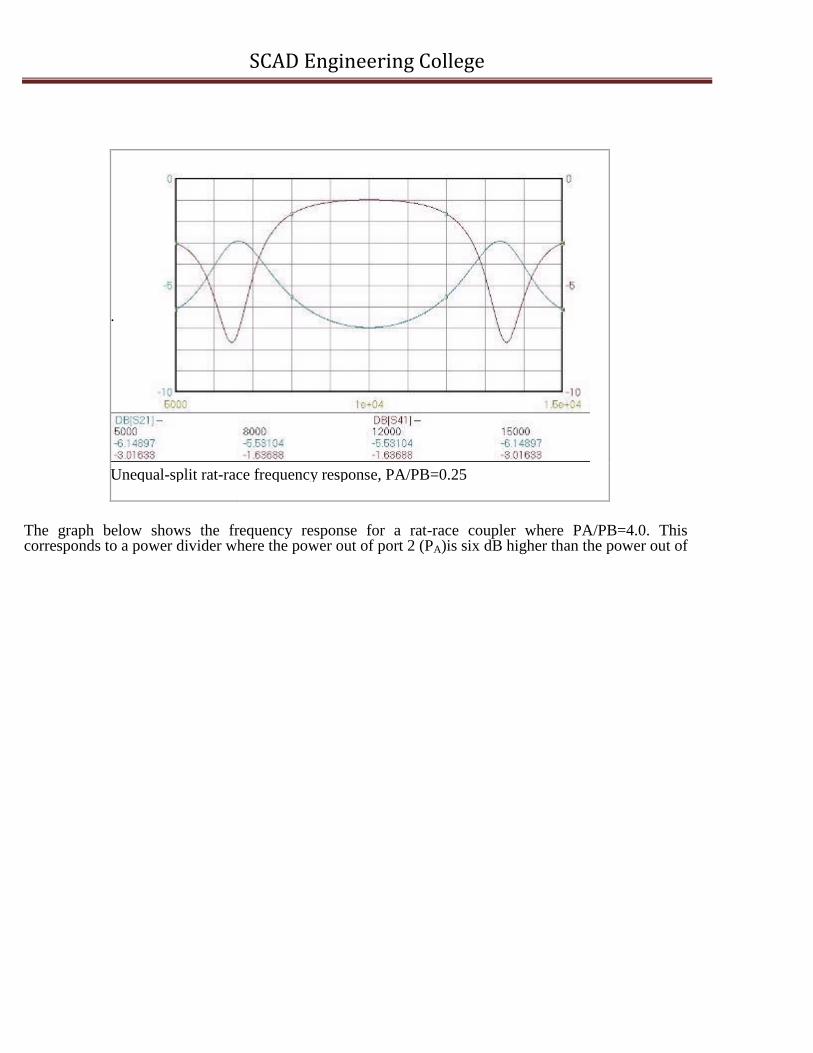
Unequal-split rat-race frequency response, PA/PB=0.25
The graph below shows the frequency response for a rat-race coupler where PA/PB=4.0. This corresponds to a power divider where the power out of port 2 (PA)is six dB higher than the power out of

SCAD Engineering College
port 4 (PB). The line impedances are opposite to the case where PA/PB=0.25; here Z0A=55.9 ohms, and Z0B= 111.6 ohms.
They couple part of the transmission power in a transmission line by a known amount out
through another port, often by using two transmission lines set close enough together such that energy passing through one is coupled to the other. As shown in Figure 1, the device has four ports: input, transmitted, coupled, and isolated. The term "main line" refers to the section between ports 1 and 2. On some directional couplers, the main line is designed for high power operation (large connectors), while the coupled port may use a small SMA connector. Often the isolated port is terminated with an internal or external matched load (typically 50 ohms). It should be pointed out that since the directional coupler is a linear device, the notations on Figure 1 are arbitrary. Any port can be the input, (as in Figure 3) which will result in the directly connected port being the transmitted port, the adjacent port being the coupled port, and the diagonal port being the isolated port.
Physical considerations such as internal load on the isolated port will limit port operation. The coupled output from the directional coupler can be used to obtain the information (i.e., frequency and power level) on the signal without interrupting the main power flow in the system (except for a power reduction - see Figure 2). When the power coupled out to port three is half the input power (i.e. 3 dB below the input power level), the power on the main transmission line is also 3 dB below the input power and equals the coupled power. Such a coupler is referred to as a 90 degree hybrid, hybrid, or 3 dB Common properties desired for all directional couplers are wide operational bandwidthhighdirectivity, and a good impedance match at all ports when the other ports are terminat d in matched loads. These performance characteristics of hybrid or non-hybrid directional coupl rs are s lf- xplanatory. Some other general characteristics will be discussed below. coupler. The frequency range for coaxial couplers specified by manufacturers is that of the c upling arm. The main arm response is much wider (i.e. if the spec is 2-4 GHz, the main arm could perate at 1
or 5 GHz - see Figure 3). However it should be recognized that the coupled response is peri dic with
frequency. For example, a λ/4 coupled line coupler will have responses at nλ/4 where n is an dd
integer.
frequency band center. For ex.mple,10dBcoupling+/-0.5dBmeansthatthedirectional coupler can have
9.5 dB to 10.5 dB coupling at the frequency band center. The accuracy is due to dimensional
Coupling factor The coupling factor is defined as: where P1 is the input power at port 1 and P3 is the o tp t power from the coupled port (see Figure 1)
The coupling factor represents the primary property of a directional coupler. Coupling is not constant, but varies with frequency. While different designs may reduce the variance, a perfectly flat coupler theoretically cannot be built Direction l couplers are specified in terms of the coupling accuracy at the

SCAD Engineering College
Loss
tolerances that can be held for the spacing of the two coupled lines. Another coupling specification
is frequency sensitivity. A larger frequency sensitivity will allow a larger frequency band of operation.
Multiple quarter- avelength coupling sections are used to obtain wide frequency bandwidth directional
couplers. Typically this type of directional coupler is designed to a frequency bandwidth ratio and a
maximum coupling ripple ithin the frequency band. For example a typical 2:1 frequency bandwidth
coupler design that produces a 10 dB coupling with a +/- 0.1 dB ripple would, using the previous accuracy
specification, be said to have 9.6 +/- 0.1 dB to 10.4 +/- 0.1 dB of coupling across the frequency range. In an ideal directional coupler, the main line loss from port 1 to port 2 (P1 - P2) due to power coupled to the coupled output port is: Isolation
Isolation of a directional coupler.cnbedefinedasthedifferenceinsignallevelsindB between
the input port and the Isolationcanalsobedefinedbetween the two output ports. In this case, one of
the output ports is used as the input; the other is considered the output port while the other two
ports (input and isolated) ed loads.
Consequently: The isolation between the input and the isolated ports may be different from the isolation
between the two output ports. For example, the isolation between ports 1 and 4 can be 30 dB while the isolation between ports 2 and 3 can be a different value such as 25 dB. If both isolation measurements are not available, they can be assumed to be equal. If neither are available, an estimate of the isolation is the coupling plus return loss (Standing wave ratio). The isolation should be as high as possible. In actual couplers the isolated port is never completely isolated. Some RF power will always be present. Waveguide directional couplers will have the best isolation.
If isolation is high, directional couplers are excellent for combining sign ls o feed a single line to
a receiver for two-tone receiver tests. In Figure 3, one signal enters port P3 nd one enters port P2, while both exit port P1. The signal from port P3 to port P1 will experience 10 dB of loss, and the signal from port P2 to port P1 will have 0.5 dB loss. The internal load on the isolated port will dissipate the signal losses from port P3 and port P2. If the isolators in Figure 3 are neglected, the isolation measurement (port P2 to port P3) determines the amount of power from the signal generator F2 that will be injected into the signal generator F1. As the injection level increases, it may cause modulation of signal generator F1, or even injection phase locking. Because of the symmetry of the directional coupler, the reverse injection will happen with the same possible mod lation problems of signal generator F2 by F1. Therefore the isolators are used in Figure 3 to effectively increase the isolation (or directivity) of the directional coupler. Consequently the injection loss will be the isolation of the directional coupler plus

SCAD Engineering College
the reverse isolation of the isolator. .
Directivity
SCAD Engineering College
The directivity should be as high as possible. Waveguide directional couplers will have the best directivity. Directivity is not directly measurable, and is calculated from the isolation and coupling measurements as:
Directivity (dB) = Isolation (dB) - Coupling (dB)
Hybrids
The hybrid coupler, or 3 dB directional coupler, in which the two outputs are of equal amplitude takes many forms. Not too long ago the quadrature (90 degree) 3 dB coupler with outputs 90 degrees ut f phase was what came to mind when a hybrid coupler was mentioned. Now any mat hed 4-p rt with isolated arms and equal power division is called a hybrid or hybrid coupler. Today the hara terizing feature is the phase difference of the outputs. If 90 degrees, it is a 90 degree hybrid If 180 degrees, it is
a 180 degree hybrid. Even the Wilkinson power divider which has 0 degrees pha e difference is actually
a hybrid although the fourth arm is normally imbedded.
.
Applications of the hybrid include monopulse comparators, mixers, pow r combin rs, dividers, modulators, and phased array radar antenna systems.
This terminology defines the power difference in dB between the two output ports of a 3 dB hybrid. In an ideal hybrid circuit, the difference should be 0 dB. However, in a practical device the amplitude balance is frequency dependent and departs from the ideal 0 dB difference.
Phase balance
Amplitude bance

SCAD Engineering College
The phase properties of a 90 degree hybrid coupler can be used to great advantage in microwave circuits. For example in a balanced microwave amplifier the two input stages are fed through a hybrid coupler. The FET device normally has a very poor match and reflects much of the incident energy. However, since the devices are essentially identical the reflection coefficients from each device are equal. The reflected voltage from the FETs are in phase at the isolated port and are 180 degrees different at the input port. Therefore, all of the reflected power from the FETs goes to the load at the isolated port and no power goes to the input port. This results in a good input match (low VSWR).
Both in-phase (Wilkinson) and quadrature (90°) hybrid couplers may be
u d for coherent power divider If phase matched lines are used for an antenna input to a 180° hybrid coupler as shown in Figure 4, a null will occur directly between the antennas. If you want to receive a signal in that positi n, y u w uld have to either change the hybrid type or line length. If you want to reject a signal from a given directi n, or create the difference pattern for a monopulse radar, this is a good approach.
applications. The Wilkinson power divider has low VSWR at all por s and high i olation between output ports. The input and output impedances at each port are designed o be qual o the characteristic impedance of the microwave system. A typical power divider is shown in Figure 5. Ideally, input power would be divided equally between the split po erequally,butbecauseof the different field configurations at the junction, the electric fields at the output arms are in-phase for the H-Plane tee and are anti-phase for the E-Plane tee. The combination of these t o tees to form a hybrid tee allowed the realization of a four-port component which could perform the vector sum (Σ) and difference (Δ) of two coherent microwave signals. This device is known as the magic tee. output ports. Dividers are made up of multiple couplers and, like couplers, may be reversed and used as multiplexers. The dra back . is that for a four channel multiplexer, the output consists of only 1/4 the
Other power dividers

SCAD Engineering College
power from each, and is relatively inefficient. Lossless multiplexing can only be done with filter networks.
Coherent po er division as first accomplished by means of simple Tee junctions. At microwave frequencies, aveguide tees have two possible forms - the H-Plane or the E-Plane. These two junctions
SCAD Engineering College
Low frequency directional couplers
For lower frequencies a compact broadband implementation by means of unidirectional couplers (transformers) is possible. In the figure a circuit is shown which is meant for weak coupling and can be understood along these lines: A signal is coming in one line pair. One transformer reduces the voltage of the signal the other reduces the current. Therefore the impedance is matched. The same argument holds for every other direction of a signal through the coupler. The relative sign of the induced voltage and current determines the direction of the outgoing signal.
coupled port (-90 degree transmission angle compared to through port)
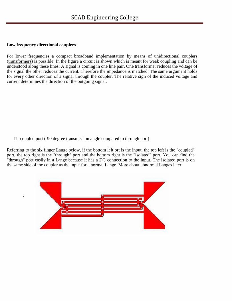
Referring to the six finger Lange below, if the bottom left ort is the input, the top left is the "coupled" port, the top right is the "through" port and the bottom right is the "isolated" port. You can find the "through" port easily in a Lange because it has a DC connection to the input. The isolated port is on the same side of the coupler as the input for a normal Lange. More about abnormal Langes later!
.
SCAD Engineering College
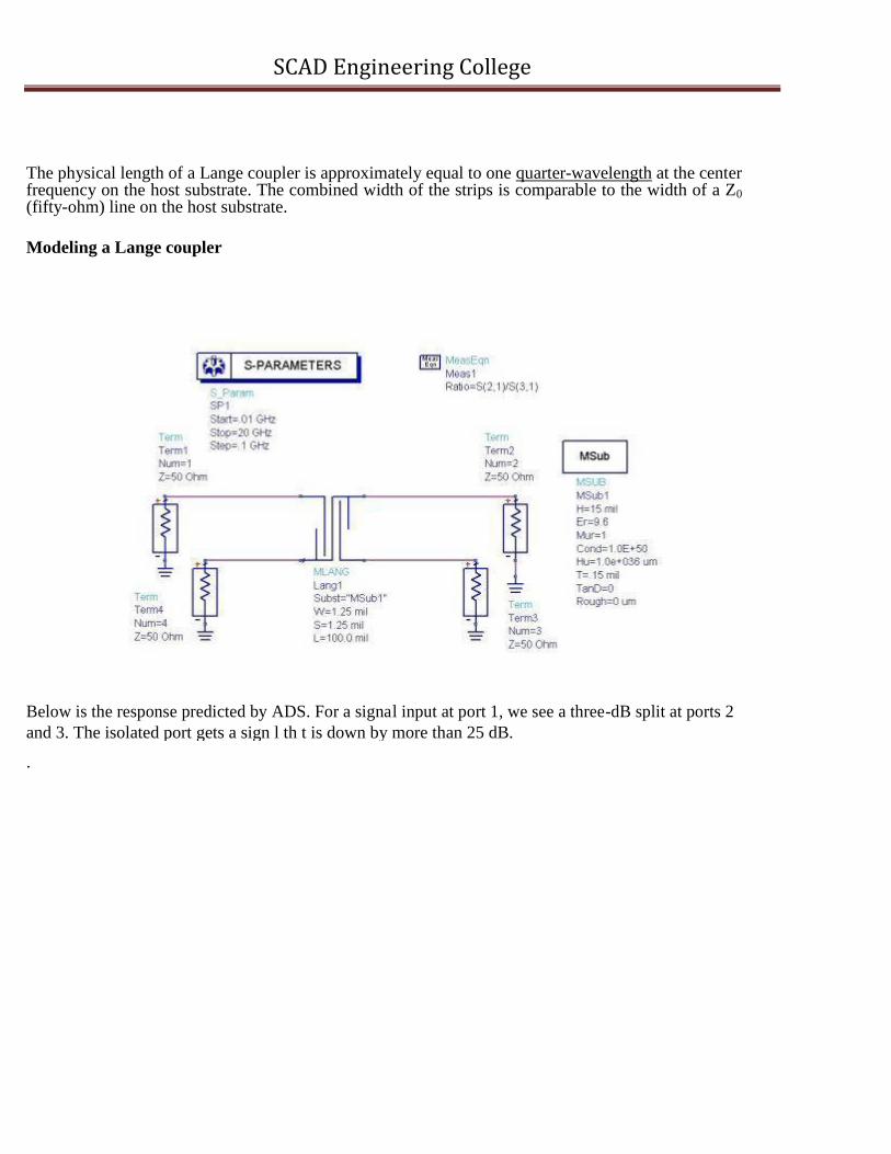
The physical length of a Lange coupler is approximately equal to one quarter-wavelength at the center frequency on the host substrate. The combined width of the strips is comparable to the width of a Z0 (fifty-ohm) line on the host substrate.
Modeling a Lange coupler
Below is the response predicted by ADS. For a signal input at port 1, we see a three-dB split at ports 2
and 3. The isolated port gets a sign l th t is down by more than 25 dB.
.

SCAD Engineering College
One more important plot is the phase difference between the output ports. Here is one of the major attractions to the Lange coupler, you won't see such a beautiful quadrature response on a branchline coupler!
\
Now let's play around with the gap dimension. Below are two respons , he first one the gap has been
increased to 1.5 mils. Notice the coupled port receives less power h n he hrough port. This coupler would be called "under-coupled". The next figureshoswhathappens when the gap dimension is reduced to 1.0 mils. Now we see an "over-
coupled" response. This is often the most desirable case, especially when your application is wide band.
The "coupling error", defined as the difference in magnitude between the two output ports, is less than
1.0 dB from 8 to 16 GHz, an octave of bandwidth. Referring to the first case where exactly 3 dB was
achieved at 12 GHz, the coupling error of 1 dB is only maintained from 9 to 15 GHz.

SCAD Engineering College
Lange couplers have been used from UHF to Q-band, perhaps higher. But as you go up in frequency, you'll need to reduce your substrate height to get microstrip to beh ve (see microstrip height rule of thumb). Reduced height means reduced strip width, which is the ultim te limitation. At some point the strips get so narrow that even if they don't fail your design rules, they will start to become lossy because there just isn't much metal to provide a conductor.
Langes on alumina are usually restricted to applications where the substrate is 15 mils or thicker; this means you'll see alumina Langes operate no higher than 25 GHz. If you attempted to make a Lange on 10-mil alumina, the strip widths would need to be less than 1 mil (25 microns).
In MMIC applications, Langes can be made on 4-mil substrates, but it is a fools errand to try to make them on 2-mil substrates. According to o r r le of thumb, that means you'll never see a Lange above 80
GHz (four mil GaAs craps out there) If you ttempted to make a Lange on 2-mil GaAs, the strip widths would need to be about five microns Forget boutit!
HYBRID (3 DB) COUPLERS.
Hybrid couplersarethespecialcase of a four-port directional coupler that is designed for a 3-dB (equal) power split. Hybrids come in two types, 90 degree or quadrature hybrids, and 180 degree hybrids. Why isn't there a "45 degree hybrid" you ask? Maybe it it wouldn't isolate the fourth port! Anyone that can submit a proof of this statement will win a gift!
All of the couplers discussed on this page have separate pages that go into detail on their operation. This page will help tie the entire mess together.
180 degree hybrid couplers
Limitations of Lange couplers

SCAD Engineering College
These include rat-race couplers and waveguide magic tees. Here we will look at the rat-race and introduce the vector and shorthand notation that is often used when referring to 180 degree hybrid couplers.
. Here's a plot that sho s the ideal, "classic" rat-race response (equal split at center frequency).

SCAD Engineering College
The rat-race gives about 32% bandwidth for a phase error of +/-10 d gr s from the ideal 180
degree split.
These are often called quadrature couplers, and include Lange couplers, the branchline coupler,
overlay
couplers, edge couplers, and short-slot hybrid co lers. Here we will just look at a branchline, and show you some of the "short hand" notation that is often sed when referring to hybrids.
Below the branchline is used as a combiner. The inp t signals are vectors of magnitude A and B,
then the outputs are as shown. Note th t bec se we are dealing with voltages, the outputs have a
square- root-of-two factor. Power is split ex ctly in h lf (-3 dB), equal to the square of the voltages.
Now let's look at it as a divider. Here only an input signal is present at port A. It splits by 3 dB at the two outputs, and is isolated from Port B (ideally zero energy comes out this port).
90 degree hybrid couplers

SCAD Engineering College
region. The generated electron . immedi tely moves into the region, while the generated holes drift across
the p region. The time required for the hole to reach the contact
constitutes the transit time delay. They operate at frequencies between about 3 and 100 GHz or more. A m in advantage is their high power capability. These diodes are used in a variety of applic tions from
low power radar systems to alarms. A major drawback of using IMPATT diodes is the high level of ph se noise they generate. This results from the statistical nature of the avalanche process. Nevertheless these diodes make excellent microwave generators for many applications. The IMPATT diode family includes many different j nctions and metal semiconductor devices. The first IMPATT oscillation was obtained from a simple silicon p-n junction diode biased into a reverse avalanche break down and mounted in microwave cavity. Because of the strong dependence of the
ionization coefficient on the electric field, most of the electron–hole pairs are generated in the high field
The original proposal for a micro ave device of the IMPATT type was made by Read and involved a
structure.TheReaddiodeconsists of two regions as illustrated in figure. (i) The Avalanche region (p1 –
region with relatively high doping and high field, ), in which avalanche multiplication occurs and (ii) the
drift region (p2 – region ith essentially intrinsic doping and constant field, , in which the generated holes
drift to ards the - contact. Of course, a similar device can be built with the configuration, in which
electrons generated from the avalanche multiplication drift through the intrinsic region.
A fabricated IMPATT diode generally is mounted in a micro wave package. The diode is mounted with its high – field region close to the Copper heat sink so that the heat generated at the junction can be
Device structure
IMPATT diode

SCAD Engineering College
conducted away readily. Similar microwave packages are used to house other microwave devices.
Principle of operation
At breakdown, the n – region is punched through and forms the avalanche region of the diode. The high resistivity i – region is the drift zone through which the avalanche generated electrons move toward the anode. Now consider a dc bias VB, just short of that required to cause breakdown, applied to the diode in the figure. Let an ac voltage of sufficiently large magnitude be superimposed on the dc bias, such that
during the positive cycle of the ac voltage, the diode is driven deep into the avalanche breakdown. At t=0, the ac voltage is zero, and only a small pre-breakdown current flows through the diode. As t
increases, the voltage goes above the breakdown voltage and secondary electron-hole pairs are produced by impact ionization. As long as the field in the avalanche region is maintain above the breakd wn field
, the electron-hole concentration grow exponentially with t. Similarly this concentration decay
exponentially with time when the field is reduced below at the negative swing of the ac v ltage. The holes generated in the avalanche region disappear in the p+ region and are collected by the ath de. The
electrons are injected into the i – zone where they drift toward the n+ region. Then, the field in the avalanche region reaches its maximum value and the population of the electron-hole pairs starts building up. At this time, the ionization coefficients have their maximum values. Although follow the electric . com field instantaneously the generated electron concentration does not b cause it al o depends on the number of electron-hole pairs already present in the avalanche region. H nc , he l ctron concentration at will have a small value. Even after the field has passed its maximum valu , he l ctron-hole
concentration continues to grow because the secondary carrier gener ion r e still remains above its average value. For this reason, the electron concentration in the v l nche region attains its maximum value at , when the field has dropped to its average value. Thus, it is cle r that the avalanche region introduces a 90
o phase shift between the ac signal and the electron concentration in this region.
With a further increase in t, the ac voltage becomes negative, and the field in the avalanche region drops below its critical value. The electrons in the avalanche region are then injected into the drift zone which induces a current in the external circuit which has a hase o osite to that of the ac voltage. The ac field, therefore, absorbs energy from the drifting electrons as they are decelerated by the decreasing field. It is clear that an ideal phase shift between the diode c rrent and the ac signal is achieved if the thickness of the drift zone is such that the bunch of electron is collected at the n
+ - anode at when the ac voltage goes
to zero. This condition is achieved by m king the length of the drift region equal to the wavelength of the signal. This situation produces n dditional phase shift of 90
o between the ac voltage and the diode

SCAD Engineering College

SCAD Engineering College
UNIT IVMICROWAVE LINEAR-BEAM TUBES & MICROWAVE CROSSED-FIELD TUBES Klystron
A klystron is a specialized linear-beam vacuum tube (evacuated electron tube). The pseudo-Greek word klystron comes from the stem form κλυσ- (klys) of a Greek verb referring to the action of waves breaking against a shore, and the end of the word electron.
The brothers Russell and Sigurd Varian of Stanford University are generally considered to be the inventors of the klystron. Their prototype was completed in August 1937. Upon publication in 1939,
[1]
news of the klystron immediately influenced the work of US and UK researchers working on radar equipment. The Varians went on to found Varian Associates to commercialize the techn l gy (f r
example to make small linear accelerators to generate photons for external beam radiati n therapy). In
their 1939 paper, they acknowledged the contribution of A. Arsenjewa-Heil and O. Heil (wife and
husband) for their velocity modulation theory in 1935.[2]
During the second World War, the Axis powers relied mostly on (then low-powered) kly tron
. technology for their radar system microwave generation, while the Allies u ed the far more powerful but
com frequency-drifting technology of the cavity magnetron for microwave g n ration. Kly tron tube
SCAD Engineering College
Explanation . technologies for very high-power applications, such as synchrotrons and radar syst ms, have since been
developed.
Introduction
Klystrons are used as an oscillator (such as the reflex klystron) or amplifier at microwave and radio frequencies to produce both low-power reference signals for superheterodyne radar receivers and to produce high-power carrier waves for comm nications and the driving force for linear accelerators. All modern klystrons are amplifiers, since reflex klystrons have been surpassed by alternative technologies. Klystron amplifiers have the advantage (over the magnetron) of coherently amplifying a reference signal so its output may be precisely controlled in amplit de, frequency and phase. Many klystrons have a waveguide for coupling microw ve energy into and out of the device, although it is also quite common
for lower power and lower frequency klystrons to se coaxial couplings instead. In some cases a
coupling probe is used to couple the microw ve energy from a klystron into a separate external
waveguide. KlystronsamplifyRFsignalsby extracting energy from a DC electron beam. A beam of electrons is
produced by a thermionic cathode (a heated pellet of low work function material), and accelerated to
high voltage (typically in the tens of kilovolts). This beam is then passed through an input cavity. RF
energy is fed into the input cavity at, or near, its natural frequency to produce a voltage which acts on
the electron beam. The electric field causes the electrons to bunch: electrons that pass through during an
opposing electric field are accelerated and later electrons are slowed, causing the previously continuous
electron beam to form bunches at the input frequency. To reinforce the bunching, a klystron may
contain additional "buncher" cavities. The electron bunches excite a voltage on the output cavity, and
the RF energy developed flows out through a waveguide. The spent electron beam, which now contains
less energy than it started with, is destroyed in a collector.

SCAD Engineering College
Two-cavity klystron amplifier
. more powerthanthereflexklystron—typically watts of output rather than
milliwatts. Since there is no In the two-chamber klystron, the electron beam is injected into a resonant cavity. The electron beam, accelerated by a positive potential, is constrained to travel through a cylindrical drift tube in a straight path by an axial magnetic field. While passing through the first c vi y, he electron beam is velocity modulated by the weak RF signal. In the moving frame of the electron be m, the velocity modulation is equivalent to a plasma oscillation, so in a quarter of one period of the pl sma frequency, the velocity modulation is converted to density modulation, i.e. bunches of electrons. As the bunched electrons enter the second chamber they induce standing waves at the same frequency as the input signal. The signal induced in the second chamber is much stronger than that in the first.
Two-cavity klystron oscillator
The two-cavity amplifier klystron is readily t rned into an oscillator klystron by providing a feedback loop between the input and output c vities. Two-cavity oscillator klystrons have the advantage of being among the lowest-noise microw ve sources vailable, and for that reason have often been used in the
illuminator systems of missile t rgeting r d rs. The two-cavity oscillator klystron normally generates
reflector, only one high-voltage supply is to cause the tube to oscillate, the voltage must be adjusted to a particular value. This is because the electron beam must produce the bunched electrons in the second cavity in order to generate output power. Voltage must be adjusted by varying the velocity of the electron beam to a suitable level due to the fixed physical separation between the two cavities. Often several "modes" of oscillation can be observed in a given klystron.
Reflex klystron

SCAD Engineering College
In the reflex klystron (also known as a 'Sutton' klystron after its inventor), the electronbeampasses through
a single resonant cavity. The electrons are fired into one end of the tube by an electron gun. After passing
through the resonant cavity they are reflected by a negativ ly charg d reflector electrode for another pass
through the cavity, where they are then collected. The l c ron b am is velocity variation in frequency bet een.halfpowerpoints—thepointsintheoscillatingmode where the power
output is half the maximum output in the mode. It should be noted that the frequency of oscillation is
modulated when it first passes through the cavity. The formation of l c ron bunch s takes place in the drift space between the reflector and the cavity. The voltage on the reflec or must be adjusted so that the bunching is at a maximum as the electron beam re-enters the reson nt c vity, thus ensuring a maximum
of energy is transferred from the electron beam to the RF oscill tions in the cavity.The voltage should always be switched on before providing the input to the reflex klystron as the whole function of the
reflex klystron would be destroyed if the supply is rovi ed after the input. The reflector voltage may be varied slightly from the optimum value, which results in some loss of output power, but also in a variation in frequency. This effect is used to good advantage for automatic frequency control in receivers, and in frequency modulation for transmitters. The level of modulation applied for
transmission is small enough that the power o tp t essentially remains constant. At regions far from the optimum voltage, no oscillations are obtained at all. This tube is called a reflex klystron because it repels the input supply or performs the opposite f nction of a [Klystron].
There are often several regions of reflector voltage where the reflex klystron will oscillate; these are referred to as modes. The electronic tuning r nge of the reflex klystron is usually referred to as the dependentonthereflectorvoltage, and varying this provides a crude method of frequency modulating
the oscillation frequency, albeit with accompanying amplitude modulation as well.
Modern semiconductor technology has effectively replaced the reflex klystron in most applications.
Multicavity klystron
In all modern klystrons, the number of cavities exceeds two. A larger number of cavities may be used to increase the gain of the klystron, or to increase the bandwidth.

SCAD Engineering College
SCAD Engineering College Tuning a klystron
Some klystrons have cavities that are tunable. Tuning a klystron is delicate work which, if not done properly, can cause damage to equipment or injury to the technician. By changing the frequency of the individual cavities, the technician can change the operating frequency, gain, output power, or bandwidth of the amplifier. The technician must be careful not to exceed the limits of the graduations, or damage to the klystron can result.
Manufacturers generally send a card with the unique calibrations for a klystron's performance characteristics, that lists the graduations that are to be set, for any given frequency. No two klystr ns are alike (even when comparing like part/model number klystrons) so that every card is specific to the individual unit. Klystrons have serial numbers on each of them that distinguishes them uniquely, and f r which manufacturers may (hopefully) have the performance characteristics in a database If not, loss of the calibration card may be an insoluble problem, making the klystron unu able or perform marginally In an optical klystron the cavities.rereplcedwithundulators.Veryhighvoltagesareneeded. The electron gun, the drift tube and the collector re still used. un-tuned.
.
com
Other precautions taken when tuning a klystron include using nonferrous ools. If f rrous (magnetically
reactive) tools come too close to the intense magnetic fields that con ain he l ctron beam (some
klystrons employ permanent magnets, which can not be turned off) he ool can be pulled into the unit by the intense magnetic force, smashing fingers, hurting the technici n, or damaging the klystron. Special lightweight nonmagnetic tools made of beryllium alloy h ve been used for tuning U.S. Air Force klystrons.
Precautions are routinely taken when transporting klystron evices in aircraft, as the intense magnetic
field can interfere with magnetic navigation equi ment. S ecial overpacks are designed to help limit this
field "in the field," and thus transport the klystron safely.
Optical klystron
Floating drift tube klystron The floatingdrifttubeklystronhas a single cylindrical chamber containing an electrically isolated central
tube. Electrically, this is similar to the two cavity oscillator klystron with a lot of feedback between the
t o cavities. Electrons exiting the source cavity are velocity modulated by the electric field as they travel
through the drift tube and emerge at the destination chamber in bunches, delivering power to the
oscillation in the cavity. This type of oscillator klystron has an advantage over the two-cavity klystron
on hich it is based. It only needs one tuning element to effect changes in frequency. The drift tube is
electrically insulated from the cavity walls, and DC bias is applied separately. The DC bias on the drift
tube may be adjusted to alter the transit time through it, thus allowing some electronic tuning of the
oscillating frequency. The amount of tuning in this manner is not large and is normally used for
frequency modulation when transmitting.

SCAD Engineering College
Collector
After the RF energy has been extracted from the electron beam, the beam is destroyed in a collector. Some klystrons include depressed collectors, which recover energy from the beam before collecting the electrons, increasing efficiency. Multistage depressed collectors enhance the energy recovery by "sorting" the electrons in energy bins. example, klystrons are routinely employed which have outputs in the range of 50.megawattscom(pulse)and 50 kilowatts (time-averaged) at frequencies nearing 3 GHz [1] Popular Sci nc 's "Be t of What's New Applications Klystrons produce microwave power far in excess of that developed by solid state. In m dern syste s, they are used from UHF (100's of MHz) up through hundreds of gigahertz (as in the Extended Interaction Klystrons in the CloudSat satellite). Klystrons can be found at work in radar, satellite and A traveling-wave tube (TWT).isnelectronicdeviceusedtoamplifyradiofrequency signals to high power, usually in an electronic ssembly known as a traveling-wave tube amplifier (TWTA). wideband high-power communication (very common in television broadcasting and EHF satellite terminals), and high-energy physics (particle accelerators and experimental reactor ) At SLAC, for 2007"[2][3] included a company[4] using a klystron to convert the hydrocarbons in everyday materials, automotive waste, coal, oil shale, and oil sands into natural gas and di s l fu l.
Confusion with krytron
A misleadingly similarly named tube, the krytron, is used in simple switching applications. It has recently gained fame as a rapid switch which can be used in nuclear weapons to precisely detonate explosives at high speeds, in order to start the fission rocess. Krytrons have also been used in photocopiers, raising issues of war technology transfer to countries for items such as this, which have a "dual use."
Traveling-wave tube
The TWT was invented by Rudolf Kompfner in a British radar lab during World War II, and refined by KompfnerandJohnPierceatBell Labs. Both of them have written books on the device.[1][2] In 1994, A.S. Gilmour rote a modern TWT book
[3] which is widely used by U.S. TWT engineers today, and
research publications about TWTs are frequently published by the IEEE.
Cuta ay view of a TWT. (1) Electron gun; (2) RF input; (3) Magnets; (4) Attenuator; (5) Helix coil; (6)

SCAD Engineering College
RF output; (7) Vacuum tube; (8) Collector.
The device is an elongated vacuum tube with an electron gun (a heated cathode that emits electrons) at one end. A magnetic containment field around the tube focuses the electrons into a beam, which then
SCAD Engineering College
passes down the middle of a wire helix that stretches from the RF input to the RF output, the electron beam finally striking a collector at the other end. A directional coupler, which can be either a waveguide or an electromagnetic coil, fed with the low-powered radio signal that is to be amplified, is positioned near the emitter, and induces a current into the helix.
The helix acts as a delay line, in which the RF signal travels at near the same speed along the tube as the electron beam. The electromagnetic field due to the current in the helix interacts with the electron beam, causing bunching of the electrons (an effect called velocity modulation), and the electromagnetic field due to the beam current then induces more current back into the helix (i.e. the current builds up and thus is amplified as it passes down).
A second directional coupler, positioned near the collector, receives an amplified version f the input
signal from the far end of the helix. An attenuator placed on the helix, usually between the input and
output helicies, prevents reflected wave from travelling back to the cathode.
The bandwidth of a broadband TWT can be as high as three octaves, although tuned (narrowband)
. com versions exist, and operating frequencies range from 300 MHz to 50 GHz. The voltage gain of the tube can be of the order of 70 decibels. amplification can occur via velocity.modulation.Helicalwaveguideshaveverynonlinear dispersion and thus are only narro band (but ider than klystron). A coupled-cavity TWT can achieve 15 kW output A TWT has sometimes been referred to as a traveling-wave mplifier ube (TWAT),
[4][5] although this
term was never really adopted. "TWT" is sometimes pronounced by engineers as "TWIT".[6]
Coupled-cavity TWT
Helix TWTs are limited in peak RF power by the current handling (and therefore thickness) of the helix wire. As power level increases, the wire can overheat and cause the helix geometry to warp. Wire thickness can be increased to improve matters, b t if the wire is too thick it becomes impossible to obtain the required helix pitch for proper operation. Typically helix TWTs achieve less than 2.5 kW output power.
The coupled-cavity TWT overcomes this limit by replacing the helix with a series of coupled cavities arranged axially along the beam Conceptu lly, this structure provides a helical waveguide and hence power.
Operationissimilartothatofaklystron, except that coupled-cavity TWTs are designed with attenuation
between the slow- ave structure instead of a drift tube. The slow-wave structure gives the TWT its wide
band idth. A free electron laser allows higher frequencies.
Traveling- ave tube amplifier

SCAD Engineering College
A TWT integrated with a regulated power supply and protection circuits is referred to as a traveling-wave tube amplifier
[7] (abbreviated TWTA and often pronounced "TWEET-uh"). It is used to
produce
SCAD Engineering College
high-power radio frequency signals. The bandwidth of a broadband TWTA can be as high as one octave, although tuned (narrowband) versions exist; operating frequencies range from 300 MHz to 50 GHz.
A TWTA consists of a traveling-wave tube coupled with its protection circuits (as in klystron) and regulated power supply (EPC, electronic power conditioner), which may be supplied and integrated by a different manufacturer. The main difference between most power supplies and those for vacuum tubes is that efficient vacuum tubes have depressed collectors to recycle kinetic energy of the electrons and therefore the secondary winding of the power supply needs up to 6 taps of which the helix voltage needs precise regulation. The subsequent addition of a linearizer (as for inductive output tube) can, by complementary compensation, improve the gain compression and other characteristics f the TWTA; this combination is called a linearized TWTA (LTWTA, "EL-tweet-uh").
Broadband TWTAs generally use a helix TWT, and achieve less than 2.5 kW output power TWTAs
using a coupled cavity TWT can achieve 15 kW output power, but at the expense of bandwidth. TWTAs are commonly used as amplifiers in satellite transponders, wh re he input signal is very weak and the output needs to be high power.
[8]
A TWTA whose output drives an antenna is a type of transmitter. TWTA transmitters are used
extensively in radar, particularly in airborne fire-control ra r systems, nd in electronic warfare and
control grid is usually referred to as a grid modulator.
Another major use of TWTAs is for the electromagnetic compatibility (EMC) testing industry for immunity testing of electronic devices.
[citation needed]
Cavity magnetron A cavity magnetronisahigh-po ered vacuum tube that generates coherent microwaves. They are commonly found in micro ave ovens, as well as various radar applications.
Construction and operation

SCAD Engineering College
All cavity magnetrons consist of a hot filament (cathode) kept at, or pulsed to, a high negative p
tential by a high-voltage, direct-current power supply. The cathode is built into the center of an eva uated, lobed, circular chamber. A magnetic field parallel to the filament is imposed by a permanent magnet. Where precise frequencies are.needed,otherdevicessuchastheKlystronareused.The voltage applied and
the properties of the cathode determine the
power of the device. cavity space. As electrons sweep past these openings, they induce a r sonan , high-frequency radio field in the cavity, which in turn causes the electrons to bunch into groups. A por ion of this field is extracted
with a short antenna that is connected to a waveguide (a met l tube usu lly of rectangular cross section). The waveguide directs the extracted RF energy to the load, which m y be cooking chamber in a microwave oven or a high-gain antenna in the case of ra ar. A cross-sectional diagram of a resonant cavity magnetron. Magnetic field is perpendicular to the plane of the diagram.
The sizes of the cavities determine the resonant freq ency, and thereby the frequency of emitted microwaves. However, the frequency is not precisely controllable. This is not a problem in many uses such as heating or some forms of r d r where the receiver can be synchronized with an imprecise output. The magnetron is a fairly efficient device. In a microwave oven, for instance, a 1,100 Watt input will generally create about 700 Watts of microwave energy, an efficiency of around 65%. Modern, solid- state, microavesourcesatthis frequency typically operate at around 25 to 30% efficiency and are used
primarily because they can generate a wide range of frequencies. Thus, the magnetron remains in
widespread use in roles hich require high power, but where precise frequency control is unimportant.
Applications
Magnetron with magnet in its mounting box. The horizontal plates form a Heatsink, cooled by airflow from a fan
Radar
In radar devices the waveguide is connected to an antenna. The magnetron is operated with very short pulses of applied voltage, resulting in a short pulse of microwave energy being radiated. As in all radar systems, the radiation reflected off a target is analyzed to produce a radar map on a screen.
Heating
Magnetron with section removed (magnet is not shown)

SCAD Engineering College
In microwave ovens the waveguide leads to a radio frequency-transparent port into the cooking chamber. It is important that there is food in the oven when it is operated so that these waves are absorbed, rather than reflecting into the waveguide where the intensity of standing waves can cause arcing. The arcing, if allowed to occur for long periods, will destroy the magnetron. If a very s all object is being microwaved, it is recommended that a glass of water be added as an energy sink, although care must be taken not to "superheat" the water.
History
.
com
The oscillation of magnetrons was first observed and noted by Augustin Žáč k, profe or at the Charles
University, Prague in the Czech Republic, although the first simple, wo-pole magn trons were developed in the 1920s by Albert HullatGeneralElectric'sResearchLaboraoris(Schenectady, New York), as an outgrowth of his work on the magnetic control of v cuum ub s in an attempt to work around the patents held by Lee De Forest on electrostatic control. The wo-pole magnetron, also known as a split-anode magnetron, had relatively low efficiency. The c vity version (properly referred to as a resonant-cavity magnetron) proved to be far more useful.
There was an urgent need during radar development in World War II for a high-power microwave generator that worked in shorter wavelengths—around 10 cm (3 GHz) rather than 150 cm—(200 MHz) available from tube-based generators of the time. It was known that a multi-cavity resonant magnetron had been developed in 1935 by Hans Hollmann in Berlin. However, the German military considered its frequency drift to be undesirable and based their radar systems on the klystron instead. It was primarily for this reason that German night fighter radars were not a match for their British counterparts. In 1940, at the University of.Birmingh m in the UK, John Randall and Dr. Harry Boot produced a working prototype similar to Hollm n's c vity magnetron, but added liquid cooling and a stronger cavity. RandallandBootsoonmanaged to increase its power output 100 fold. Instead of giving up on the magnetron due to its frequency inaccuracy, they sampled the output signal and synced their receiver to whatever frequency as actually being generated.
Because France had just fallen to the Nazis and Britain had no money to develop the magnetron on a massive scale, Churchill agreed that Sir Henry Tizard should offer the magnetron to the Americans in exchange for their financial and industrial help. By September, the Massachusetts Institute of Technology had set up a secret laboratory to develop the cavity magnetron into a viable radar. Two months later, it as in mass production, and by early 1941, portable airborne radar were being installed into American and British planes.
[1]
An early 6 kW version, built in England by the GEC Research Laboratories, Wembley, London, was given to the US government in September 1940. It was later described as "the most valuable cargo ever brought to our shores" (see Tizard Mission). At the time the most powerful equivalent microwave

SCAD Engineering College
producer available in the US (a klystron) had a power of only ten watts. The cavity magnetron was widely used during World War II in microwave radar equipment and is often credited with giving Allied radar a considerable performance advantage over German and Japanese radars, thus directly influencing the outcome of the war.
Short-wave, centimetric radar, which was made possible by the cavity magnetron, allowed for the detection of much smaller objects and the use of much smaller antennas. The combination of the small-cavity magnetron, small antennas, and high resolution allowed small, high quality radars to be installed in aircraft. They could be used by maritime patrol aircraft to detect objects as small as a submarine periscope, which allowed aircraft to attack and destroy submerged submarines which had previ usly been undetectable from the air. Centimetric contour mapping radars like H2S improved the accuracy f Allied bombers used in the strategic bombing campaign. Centimetric gun-laying radars were likewise far more accurate than the older technology. They made the big-gunned Allied battleships m re deadly and, along with the newly developed proximity fuse, made anti-aircraft guns much more dangerous to attacking aircraft. The two coupled together and used by anti-aircraft batterie , pla ed along the flight
path of German V-1 flying bombs on their way to London, are credited with de troying many of the
.
flying bombs before they reached their target.
Since then, many millions of cavity magnetrons have been manufac ur d; some for radar, but the vast majority for microwave ovens. The use in radar itself has dwindled o some extent, as more accurate
signals have generally been needed and developers have moved to klystron and traveling wave tube systems for these needs.
Among more speculative hazards, at least one in artic lar is well known and documented. As the lens
of the eye has no cooling blood flow, it is partic larly prone to overheating when exposed to microwave
radiation. This heating can in turn lead to a higher incidence of cataracts in later life.[citation needed]
A microwave oven with a warped door or poor microwave sealing can be hazardous.
There is also a considerable electric l h z rd round magnetrons, as they require a high voltage power supply. Operating a magnetron with the protective covers and interlocks bypassed should therefore be Some magnetronshaveceramic insulators with a bit of beryllium oxide (beryllia) added—these ceramics often appear some hat pink or purple-colored (see the photos above). Note that beryllium oxide is white, so relying on the color to identify its presence would be unwise. The beryllium in this ceramic is a serious chemical hazard if crushed and inhaled, or otherwise ingested. Single or chronic exposure can lead to berylliosis, an incurable lung condition. In addition, beryllia is listed as a confirmed human carcinogen by the IARC; therefore, broken ceramic insulators or magnetrons should not be directly handled. avoided.
Health hazards

SCAD Engineering College
.
SCAD Engineering College
UNIT V STRIP LINES and MONOLITHIC MICROWAVE INTEGRATED CIRCUITS
Microstrip If one solves the electromagnetic equations to find the field distributions, one finds.verycomnearlya completely TEM (transverse electromagnetic) pattern. This means that there are only a few regions in which there is a component of electric or magnetic field in the direction of wave propagation. There is a Microstrip transmission line is a kind of "high grade" printed circuit construction, consisting of a track of copper or other conductor on an insulating substrate. There is a "backplane" on the other side of the insulating substrate, formed from similar conductor. A picture (37kB).
Looked at end on, there is a "hot" conductor which is the track on the top, and a "return" c nduct r which is the backplane on the bottom. Microstrip is therefore a variant of 2-wire transmissi n line.
field lines at the interface, which.givesrisetoalongitudinalmagneticfieldcomponent from the second Maxwell's equation, curl E = - dB/dt picture of these field patterns (incomplete) in T C Edwards "Foundations for Micro trip Circuit Design" edition 2 page 45. See the booklist for further bibliographic details.
The field pattern is commonly referred to as a Quasi TEM p ttern. Under some conditions one has to take account of the effects due to longitudinal fields. An ex mple is geometrical dispersion, where different wave frequencies travel at different phase velocities, nd the group and phase velocities are different.
The quasi TEM pattern arises because of the interface between the dielectric substrate and the
surrounding air. The electric field lines have a discontin ity in direction at the interface. The boundary conditions for electric field are that the normal component (ie the component at right angles to the
surface) of the electric field times the dielectric constant is continuous across the boundary; thus in the dielectric which may have dielectric constant 10, the electric field suddenly drops to 1/10 of its value in air. On the other hand, the tangenti l component (parallel to the interface) of the electric field is continuous across the boundary In gener l then we observe a sudden change of direction of electric
Since some of the electric energy is stored in the air and some in the dielectric, the effective dielectric
constant fortheavesonthetransmission line will lie somewhere between that of the air and that of the
dielectric. Typically the effective dielectric constant will be 50-85% of the substrate dielectric constant. As an example, in (notionally) air spaced microstrip the velocity of waves would be c = 3 * 10^8 metres per second. We have to divide this figure by the square root of the effective dielectric constant to find the actual ave velocity for the real microstrip line. At 10 GHz the wavelength on notionally air spaced microstrip is therefore 3 cms; however on a substrate with effective dielectric constant of 7 the wavelength is 3/(sqrt{7}) = 1.13cms. Thus the maximum length for a stub to be used in stub matching,

SCAD Engineering College
which is no more than half a wavelength, is about 5.6 mm.
A set of detailed design formulae and algorithms is presented in T C Edwards, Op Cit.

SCAD Engineering College
The surface finish and flatness
The dielectric loss tangent, or imaginary part of the dielectric constant, which etscomthe dielectric
loss
The cost
The thermal expansion and conductivity
The dimensional stability with time
The surface adhesion properties for the conductor co tings
The manufacturability (ease of cutting, shaping, and rilling)
The porosity (for high vacuum applications we on't want a substrate which continually
"outgasses" when pumped) Types of substrate include plastics,sinteredceramics,glasses,andsinglecrystalsubstrates (single
crystals may have anisotropic dielectric constants; "anisotropic" means they are different along
the
different crystal directions with respect to the crystalline axes.)
Plastics are cheapDielectric constant: 2.2 (fast substrate) or 10.4 (slow substrate) o Loss tangent 1/1000 (fast substrate) 3/1000 (slow substrate) o Surface roughness about 6 microns (electroplated) o Low themal conductivity, 3/1000 watts per cm sq per degree
Ceramics are rigid and hard; they are difficult to shape, cut, and drill; they come in various purity grades and prices each having domains of application; they have low microwave loss and are reasonably non-dispersive; they have excellent thermal properties, including good dimensional stability and high thermal conductivity; they also have very high dielectric strength. They cost more than plastics. In principle the size is not limited.
o Dielectric constant 8-10 (depending on purity) so slow substrate o Loss tangent 1/10,000 to 1/1,000 depending on purity o Surface roughness at best 1/20 micron

SCAD Engineering College
SCAD Engineering College
o High thermal conductivity, 0.3 watts per sq cm per degree K Single crystal sapphire is used for demanding applications; it is very hard, needs orientation for
the desired dielectric properties which are anisotropic; is very expensive, can only be made in small sheets; has high dielectric constant so is used for very compact circuits at high frequencies; has low dielectric loss; has excellent thermal properties and surface polish.
o Dielectric constant 9.4 to 11.6 depending on crystal orientation (slow substrate) o Loss tangent 5/100,000 o Surface roughness 1/100 micron o High thermal conductivity 0.4 watts per sq cm per degree K
Single crystal Gallium Arsenide (GaAs) and Silicon (Si) are both used for monolithic icr wave
integrated circuits (MMICs).
o Dealing with GaAs first we have..... Dielectric constant 13 (slow substrate) .
Loss tangent 6/10,000 (high resistivity GaAs)
Surface roughness 1/40 micron
Thermal conductivity 0.3 watts per sq cm per degree K (high)
GaAs is expensive and piezoelectric; acoustic modes can propagate in the substrate and can couple to the electromagnetic waves on the conduc ors.
impossible small, which restricts.thepowerhndlingcapability.Fortheseapplications one often choses
fused quartz (dielectric constant 3 8)
o Now dealing with Silicon we have.....
Dielectric constant 12 (slow substrate)
Loss tangent 5/1000 (high resistivity)
Surface roughness 1/40 micron
Thermal conductivity 0.9 watts er sq cm per egree K (high) The dielectric strength of ceramics and of single crystals far exceeds the strength of plastics, and so the power handling abilities are correspondingly higher, and the breakdown of high Q filter structures correspondingly less of a problem.
It is also a good idea to have a high dielectric constant substrate and a slow wave propagation velocity; this reduces the radiation loss from the circuits. However at the higher frequencies the circuits get Cross-sectionofmicrostripgeometry. Conductor (A) is separated from ground plane (D) by dielectric
substrate (C). Upper dielectric (B) is typically air. Microstrip is a type of electrical transmission line which can be fabricated using printed circuit board [PCB] technology, and is used to convey microwave-frequency signals. It consists of a conducting strip separated from a ground plane by a dielectric layer known as the substrate. Microwave components such as antennas, couplers, filters, power dividers etc. can be formed from microstrip, the entire device existing as the pattern of metallization on the substrate. Microstrip is thus far cheaper than traditional waveguide technology, as well as being far lighter and more compact.

SCAD Engineering College
The disadvantages of microstrip compared with waveguide are the generally lower power handling capacity, and higher losses. Also, unlike waveguide, microstrip is not enclosed, and is therefore susceptible to cross-talk and unintentional radiation.
For lowest cost, microstrip devices may be built on an ordinary FR4 (standard PCB) substrate. However it is often found that the dielectric losses in FR4 are too high at microwave frequencies, and that the dielectric constant is not sufficiently tightly controlled. For these reasons, an alumina substrate is commonly used.
On a smaller scale, microstrip transmission lines are also built into microwave monolithic integrated circuits [MMIC]s.
Microstrip lines are also used in high-speed digital PCB designs, where signals need to be r uted fr m one part of the assembly to another with minimal distortion, and avoiding high cross-talk and radiation. Microstrip is very similar to stripline and coplanar waveguide [CPW], and it is po ible to integrate all
.
three on the same substrate.
Inhomogeneity
The electromagnetic wave carried by a microstrip line exists p rtly in the dielectric substrate, and partly in the air above it. In general, the dielectric constant of the substr te will be greater than that of the air, so that the wave is travelling in an inhomogeneous me ium. In consequence, the propagation velocity is somewhere between the speed of radio waves in the substrate, and the speed of radio waves in air. This behaviour is commonly described by stating the effective dielectric constant (or effective relative permittivity) of the microstrip; this being the dielectric constant of an equivalent homogeneous medium (i.e. one resulting in the same propagation velocity).
Further consequences of an inhomogeneo s medi m include:
The line is dispersive. With increasing frequency, the effective dielectric constant gradually
This
is
usuall
y
Thecharacteristicimpedance of the line changes slightly with frequency (again, even with a non-
dispersive substrate material). The characteristic impedance of non-TEM modes is not uniquely
defined, and depending on the precise definition used, the impedance of microstrip either rises,
falls, or falls then rises with increasing frequency.[3]
The low-frequency limit of the characteristic

SCAD Engineering College
impedance is referred to as the quasi-static characteristic impedance, and is the same for all
definitions of characteristic impedance.
Characteristic Impedance
SCAD Engineering College
the strip. Mitring the bend reduces the area of metallization, and so removes the excess capacitance. The percentage mitre is the cut-away fraction of the diag nal between the inner and outer corners of the un-mitred bend.
subject to and the with the substrate dielectric constant . This formula is entirely independent of . The actual range of parameters for which Douville and James present evid nce is and . They report a VSWR of better than 1.1 (i.e. a return better than -26dB) for any percentage mi r wi hin 4% (of the original d) of that given by the formula. Note that for the minimum w / h of 0.25, he p rc ntage mitre is 96%, so that the strip is very nearly cut through.
For both the curved and mitred bends, the electrical length is somewh t shorter than the physical path-length of the strip.
Monolithic Microwave Integrated Circuit
From Wikipedia, the free encyclopedia
(Redirected from MMIC)
Jump to: navigation, search
MMICs, or Monolithic Microw ve Integr ted Circuits, are a type of integrated circuit (IC) devices
that operate at microwave frequencies (300 MHz to 300 GHz).
.
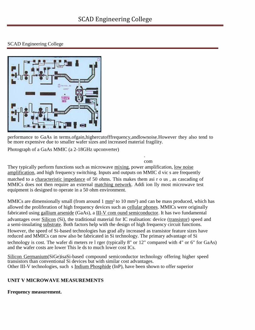
SCAD Engineering College
SCAD Engineering College performance to GaAs in terms.ofgain,highercutofffrequency,andlownoise.However they also tend to be more expensive due to smaller wafer sizes and increased material fragility.
Photograph of a GaAs MMIC (a 2-18GHz upconverter)
.
com
They typically perform functions such as microwave mixing, power amplification, low noise
amplification, and high frequency switching. Inputs and outputs on MMIC d vic s are frequently matched to a characteristic impedance of 50 ohms. This makes them asi r o us , as cascading of MMICs does not then require an external matching network. Addi ion lly most microwave test equipment is designed to operate in a 50 ohm environment.
MMICs are dimensionally small (from around 1 mm² to 10 mm²) and can be mass produced, which has allowed the proliferation of high frequency devices such as cellular phones. MMICs were originally
fabricated using gallium arsenide (GaAs), a III-V com ound semiconductor. It has two fundamental advantages over Silicon (Si), the traditional material for IC realisation: device (transistor) speed and a semi-insulating substrate. Both factors help with the design of high frequency circuit functions. However, the speed of Si-based technologies has grad ally increased as transistor feature sizes have reduced and MMICs can now also be fabricated in Si technology. The primary advantage of Si technology is cost. The wafer di meters re l rger (typically 8" or 12" compared with 4" or 6" for GaAs) and the wafer costs are lower This le ds to much lower cost ICs. Silicon Germanium(SiGe)isaSi-based compound semiconductor technology offering higher speed transistors than conventional Si devices but with similar cost advantages. Other III-V technologies, such s Indium Phosphide (InP), have been shown to offer superior
UNIT V MICROWAVE MEASUREMENTS
Frequency measurement.

SCAD Engineering College
Counters and pre-scalers for direct frequency measurement in terms of a quartz crystal reference
oscillator are often used at lower frequencies, but they give up currently at frequencies above about
10GHz. An alternative is to measure the wavelength of microwaves and calculate the frequency from the
relationship (frequency) times (wavelength) = wave velocity. Of course, the direct frequency counter
will give a far more accurate indication of frequency. For many purposes the 1% accuracy of a
wavelength measurement suffices. A resonant cavity made from waveguide with a sliding short can be
used to measure frequency to a
precision and potential accuracy
of 1/Q of the cavity, where Q is
the quality factor often in the
range 1000-10,000 for practical cavities.
Accuracy is governed by whether the graduations on the scale have been correctly.drawn with respect to
com the original standard. For example, our plastic ruler may have been put into boiling water and stretched
vernier scale may measure this.toaprecisionof1/20mm.Theexpectedprecisionofmeasurement is
therefore 1 part in 300 or about 0.33% by 1 part in 20. The measurements on this ruler may be precise to 1/2mm, but in a 10 cm measurement they will be inaccurate by 10/20 cm or 5mm, ten times as much.
In a cavity wavemeter, the precision is set by the cavity Q f ctor which sets the width of the resonance. The accuracy depends on the calibration, or even how the sc le h s been forced by previous users
winding down the micrometer against the end stop...
Wavelength measurement. Wavelength is measured by means of signal strength sampling probes which are moved in the direction of wave propagation by means of a sliding carriage and vernier distance scale. The signal strength varies because of interference between forward and backward propagating waves; this gives rise to a standing wave pattern with minima spaced 1/2 w velength. At a frequency of 10 GHz the w velength in free space is 3 cm. Half a wavelength is 15mm and a
The locationofamaximumisless precise than the location of a minimum; the indicating signal strength
meter can be set to have a gain such that the null is very sharply determined. In practice one would
average the position of t o points of equal signal strength either side of the null; and one would also
average the readings taken ith the carriage moving in positive and negative directions to eliminate
backlash errors.
Multiple readings with error averaging can reduce the random errors by a further factor of 3 for a run of 10 measurements.
"Precision" and "accuracy".

SCAD Engineering College
Signal strength measurement
The 10 GHz microwave signal in the waveguide is "chopped" by the PIN modulator at a frequency of 1kHz (audio) and the square wave which does this is provided by the bench power supply.
The detector diodes in the mounts on the wavemeter and slotted line rectify and filter this 10GHz AM signal and return a 1kHz square wave which you can observe directly on the oscilloscope. They are actually being used as "envelope detectors" as is the detector diode in your AM radio.
The VSWR indicator is a 1kHz tuned audio amplifier with 70dB dynamic range at least, and a calibrated attenuator sets its gain. The meter measures the size of the audio signal at 1kHz.
.
com
.
An X-band slotted line

SCAD Engineering College

SCAD Engineering College
.
Another example of an X-band slotted line.
.

SCAD Engineering College
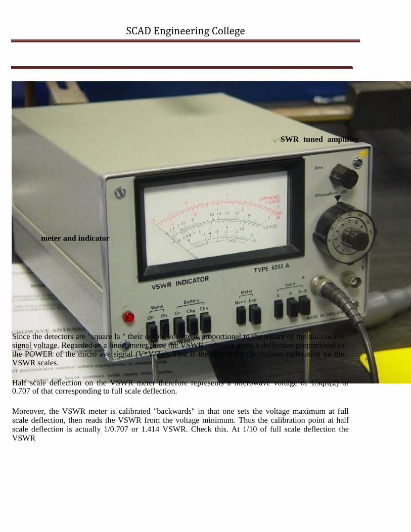
SCAD Engineering College
. SWR tuned amplifier
meter and indicator
Since the detectors are "square la " their output voltage is proportional to the square of the microwave signal voltage. Regarded as a linear meter then, the VSWR indicator gives a deflection proportional to the POWER of the micro ave signal (V*V/Zo). That is the reason for the curious calibration on the VSWR scales.
Half scale deflection on the VSWR meter therefore represents a microwave voltage of 1/sqrt(2) or 0.707 of that corresponding to full scale deflection.
Moreover, the VSWR meter is calibrated "backwards" in that one sets the voltage maximum at full scale deflection, then reads the VSWR from the voltage minimum. Thus the calibration point at half scale deflection is actually 1/0.707 or 1.414 VSWR. Check this. At 1/10 of full scale deflection the VSWR
SCAD Engineering College
calibration point is sqrt(10) or 3.16. At this point one increases the gain by a factor of 10 with the main attenuator adjustment, and reads the VSWR scale from 3.16 to 10 on the other half of the VSWR
scale. Get a demonstrator to show you how if this isn't yet clear.
Note that the gain dB scales and the attenuator on the VSWR indicator correspond to POWER of the microwave signal, not to POWER of the 1kHz audio input.
A visit to your favourite microwave book shows that a measurement of the standing wave ratio al ne is sufficient to determine the magnitude, or modulus, of the complex reflection coefficient. In turn this gives the return loss from a load directly. The standing wave ratio may be measured dire tly using a travelling signal strength probe in a slotted line. The slot in waveguide is cut so that it d es n t ut any of the current flow in the inside surface of the guide wall. It therefore does not disturb the field pattern and does not radiate and contribute to the loss. In the X band waveguide slotted lines in our lab, there is a ferrite fringing collar which additionally confines the energy to the guide. . To determine the phase of the reflection coefficient we need to find out he position of a standing wave minimum with respect to a "reference plane". The procedure is as follows:-
First, measure the guide wavelength, and record it with its associ ted ccur cy estimate.
Second, find the position of a standing wave minimum for the load being measured, in terms of the arbitrary scale graduations of the vernier scale.
Third, replace the load with a short to establish a reference lane at the load position, and measure the closest minimum (which will be a deep n ll) in terms of the arbitrary scale graduations of the vernier scale. Express the distance between the meas rement for the load and the short as a fraction of a guide wavelength, and note if the short meas rement has moved "towards the generator" or "towards the load". The distance will always be less th n 1/4 g ide wavelength towards the nearest minimum. Fourth, locate the r > 1 line on the SMITH ch rt and set your dividers so that they are on the centre of Fifth, locatetheshortcircuitpoint on the SMITH chart at which r = 0, and x = 0, and count round towards the generator or load the fraction of a guide wavelength determined by the position of the minimum. the chart at one end, and on the me sured VSWR at the other along the r > 1 line. (That is, if VSWR =
1.7, find the value r = 1.7).
. Well done. If you plot the point out from the centre of the SMITH chart a distance "VSWR" and round
Measurements of impedance and reflection coefficient.

SCAD Engineering College
as indicated you ill be able to read off the normalised load impedance in terms of the line or guide characteristic impedance. The fraction of distance out from centre to rim of the SMITH chart represents the modulus of the reflection coefficient [mod(gamma)] and the angle round from the r>1 line in degrees represents the phase angle of the reflection coefficient [arg(gamma)].

SCAD Engineering College
Microwave waveguide benches. These demonstration benches introduce the novice student to the essentials of the behaviour of microwaves in the laboratory. The wavelength is convenient at the operating frequency in X band (8-12 GHz approx) The waveguide used is WG90, so called because the principal waveguide dimension is 0.900 inches, 900 "thou" or "mils" depending on whether you are using British or American parlance. The guide wavelength at 10 GHz in WG90 is notionally 3.98 cm (the free space wavelength is 3 c ) so the standing wave pattern repeats at a distance of about 2 cm.
.
com
.

SCAD Engineering College
An X-band waveguide bench.

SCAD Engineering College
The benches include an attenuator, and an isolator. Both of these help to stop the reflected power from reaching the oscillator and pulling the frequency of the cavity and Gunn diode off tune when the load impedance is varied. There is a dual directional coupler, arranged as a pair of crossed waveguides, which samples some of the forward wave po er and couples it to a calibrated cavity wavemeter for measuring the oscillator frequency. Taken together ith a measurement of guide wavelength, we have then two independent checks on the oscillator frequency. There is also a PIN modulator which chops the 10GHz signal at a frequency of 1KHz square wave.

SCAD Engineering College
The guide wavelength is an important property to be measured, and should not be changed during the course of a series of measurements. A half guide wavelength (about 2 cm) represents a plot of once round the SMITH chart. As remarked, we can determine the position of a minimum to about 1/20mm precision, or about 1 degree of angle around the chart. That represents 0.00125 lambda error in the phase plot on the SMITH chart.
Network analysers. A network analyser makes measurements of complex reflection coefficients on 2-port
microwave networks. In addition, it can make measurements of the complex amplitude ratio between the outgoing wave on one port and the incoming wave on the other. There are thus four possible complex amplitude ratios which can be measured. If we designate the two ports 1 and 2 respectively, these ratios may be Network analysers can be automated and controlled by computer, and make mea.urementscomataseriesof different frequencies derived from a computer controlled master oscillator. Th y th n plot the s-parameters against frequency, either on a SMITH chart or directly. written s11 s12 s21 s22. These are the four "s-parameters" or "scattering parameters" for the network. Together they may be assembled into a matrix called the "s-matrix" or "scattering matrix".
The network analyser works on a different principle to the slotted line. It forms sums and
differences f the port currents and voltages, by using a cunning bridge arrangement. The phase angles are f und by using synchronous detection having in-phase and quadrature components. From the measured v ltage and currents it determines the incoming and outgoing wave amplitudes. As we recall from elsewhere in the notes, V+ = (V + ZoI)/2 and V- = (V - ZoI)/2. The important experimental technique to the use of a network n lyser lies in he calibration
procedure. It is usual to present the analyser with known scattering events, from m tched
terminations and short circuits at known places. It can then adjust its presentation of s-p r
meters for imperfections in the transmission lines connecting the analyser to the network, so
that the user never has to consider the
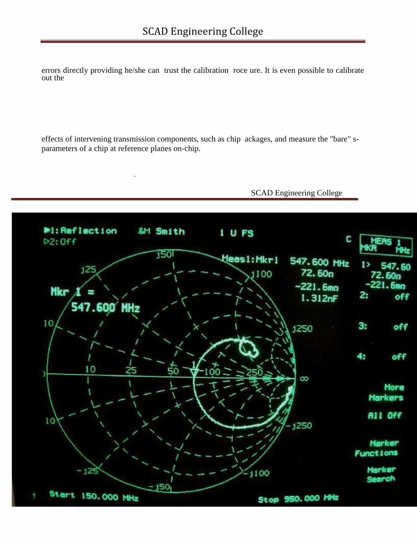
SCAD Engineering College
errors directly providing he/she can trust the calibration roce ure. It is even possible to calibrate out the
effects of intervening transmission components, such as chip ackages, and measure the "bare" s- parameters of a chip at reference planes on-chip.
.
SCAD Engineering College
.
com

SCAD Engineering College
A network analyser SMITH chart plot of a dipole
.