saturday, march 21, 2015ieee @ ucsb0 ece 92 projects in electrical and computer engineering lecture...
TRANSCRIPT

Saturday, March 21, 2015 IEEE @ UCSB 1
ECE 92ECE 92
Projects in Electrical and Computer Engineering
Projects in Electrical and Computer Engineering
Lecture 2

TransistorTransistor
Saturday, March 21, 2015 IEEE @ UCSB 2
• The transistor is a three-terminal semiconductor device.
• Can control electric current or voltage between two of the terminals.
• Used as amplifier or as switch.Field-Effect Transistors
JFET, MESFET
Depletion-mode (normally on)
n-ch p-ch
MOSFET
Depletion-mode (normally on)
Enhancement-mode (normally off)
n-ch p-ch n-ch p-ch

JFETsJFETs
Saturday, March 21, 2015 IEEE @ UCSB 3
Vgs
Gate
Source
Drain
Ids(Vgs,Vds)Vds
Gate
Source
Drain
N-ch JFET
Saturation region ID
Vgs ≤ Vt (cutoff)
Ohmic or Triode region
Vds
Vgs= Vt + 0.5
Vgs= Vt + 1.0
Vgs= Vt + 1.5
Vgs= 0 Idss
Incr
ea
sin
g
Vgs

MOSFETsMOSFETs
Saturday, March 21, 2015 IEEE @ UCSB 4
Vgs
Gate
Source
Drain
Ids(Vgs,Vds)Vds
Gate
Source
Drain
NMOS
Saturation region ID
Vgs ≤ Vt (cutoff)
Ohmic or Triode region
Vds
Vgs= Vt + 0.5
Vgs= Vt + 1.0
Vgs= Vt + 1.5
Vgs= Vt + 2.0
Incr
ea
sin
g
Vgs

BJTsBJTs
Saturday, March 21, 2015 IEEE @ UCSB 5
Base
Emitter
Collector
NPN BJT Ib
Ic=βIB
BC
E
Ic, , mA Forward active region
VCE
70 μA
Incr
ea
sin
g I
b
60 μA
50 μA
40 μA
30 μA
20 μA
10 μA
0 μA
Vce,sat
2
4
6
8

NMOS and PMOSNMOS and PMOS
Saturday, March 21, 2015 IEEE @ UCSB 6

ExampleExample
Saturday, March 21, 2015 IEEE @ UCSB 7
Find W/L and R for the circuit below assuming kn = 100 μA/V2 (transconductance), Vt = 1 V (threshold voltage), and rDS = 40 Ω (drain-to-source resistance).

Op-AmpsOp-Amps
Saturday, March 21, 2015 IEEE @ UCSB 8
• Active circuit element designed to perform mathematica operations of addition, subtraction, multiplication, division, differentiation and integration.
• Useful term: gain=amount of amplification produced by an op-amp. Defined as:

Op-AmpsOp-Amps
Saturday, March 21, 2015 IEEE @ UCSB 9

Op-AmpsOp-Amps
Saturday, March 21, 2015 IEEE @ UCSB 10
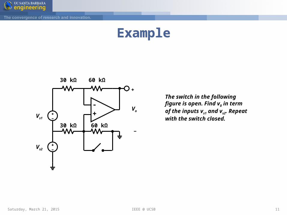
ExampleExample
Saturday, March 21, 2015 IEEE @ UCSB 11
+-
Vo
30 kΩ 60 kΩ
60 kΩ30 kΩ
Vs1
Vs2
The switch in the following figure is open. Find v0 in term of the inputs vs1 and vs2. Repeat with the switch closed.