saqib rafique - um students'...
TRANSCRIPT
MODIFICATION OF HOLE TRANSPORT LAYER
TO ENHANCE THE PERFORMANCE OF
POLYMER SOLAR CELLS
SAQIB RAFIQUE
FACULTY OF SCIENCE
UNIVERSITY OF MALAYA
KUALA LUMPUR
2017

MODIFICATION OF HOLE TRANSPORT LAYER TO
ENHANCE THE PERFORMANCE OF POLYMER
SOLAR CELLS
SAQIB RAFIQUE
THESIS SUBMITTED IN FULFILMENT OF
THE REQUIREMENTS FOR THE DEGREE OF
DOCTOR OF PHILOSOPHY
FACULTY OF SCIENCE
UNIVERSITY OF MALAYA
KUALA LUMPUR
2017
ii
UNIVERSITY OF MALAYA
ORIGINAL LITERARY WORK DECLARATION
Name of Candidate: SAQIB RAFIQUE (I.C/Passport No: AB9560243)
Registration/Matric No: SHC 140123
Name of Degree: DOCTOR OF PHILOSOPHY
Title of Project: Thesis
MODIFICATION OF HOLE TRANSPORT LAYER TO ENHANCE THE
PERFORMANCE OF POLYMER SOLAR CELLS
Field of Study: EXPERIMENTAL PHYSICS
I do solemnly and sincerely declare that:
(1) I am the sole author/writer of this Work;
(2) This Work is original;
(3) Any use of any work in which copyright exists was done by way of fair
dealing and for permitted purposes and any excerpt or extract from, or
reference to or reproduction of any copyright work has been disclosed
expressly and sufficiently and the title of the Work and its authorship have
been acknowledged in this Work;
(4) I do not have any actual knowledge nor do I ought reasonably to know that
the making of this work constitutes an infringement of any copyright work;
(5) I hereby assign all and every rights in the copyright to this Work to the
University of Malaya (“UM”), who henceforth shall be owner of the
copyright in this Work and that any reproduction or use in any form or by any
means whatsoever is prohibited without the written consent of UM having
been first had and obtained;
(6) I am fully aware that if in the course of making this Work I have infringed
any copyright whether intentionally or otherwise, I may be subject to legal
action or any other action as may be determined by UM.
Candidate’s Signature Date:
Subscribed and solemnly declared before,
Witness’s Signature Date:
Name: KHAULAH SULAIMAN (Ph.D.)
Designation: ASSOCIATE PROFESSOR
iii
ABSTRACT
Despite the fact that development of organic solar cells (OSCs) is rapidly
accelerating as the new need of green energy sources, they continue taking backstage
roll in growing markets of various photovoltaic technologies due to their limited
efficiency and stability. One of the challenges in obtaining the high performance of
OSCs is an inefficient charge extraction and transportation to the electrodes, in
particular, inability of new generation of donor polymers to obtain Ohmic contacts
between the electrodes and the photo-active layer. Poly (3, 4-ethylenedioxythiophene)
polystyrene sulfonate (PEDOT:PSS) is the current state of the art interfacial material
used to reduce these contact barriers between the photo-active layer and indium tin
oxide (ITO) electrode. However, PEDOT:PSS as a hole transport layer (HTL) also
favors device degradation due to its hygroscopic and acidic nature, resulting in severe
device instability. Combination of metal oxides and/or graphene oxide (GO) along with
PEDOT:PSS to form a composite HTL is expected to compliment the drawbacks of any
of the individual materials. This dissertation is primarily focused on identifying and
addressing the stability and degradation issues associated with bulk heterojunction
(BHJ) solar cells. In particular, vanadium pentaoxide (V2O5), and/or graphene oxide
(GO) along with the PEDOT:PSS were studied and device based on organic-inorganic
hybrid HTL were fabricated and characterised. The first part of the work is devoted to
the stability and degradation issues. Layer by layer degradation study of BHJ OSCs
with pristine PEDOT:PSS HTL was performed to identify the factors affecting device
efficiency and stability. It was demonstrated that indium diffusion from ITO anode and
oxygen ingress from atmosphere are some of the major causes of device instability,
which affect the morphological, optical, compositional and photovoltaic characteristics
of the OSCs. Another task of this work was to fabricate and study the normal

iv
architecture BHJ OSCs based on hybrid HTL consisting of PEDOT:PSS along with
V2O5, and/or GO, and compare the device performance with that of pristine
PEDOT:PSS. In this context, applicability of V2O5 incorporated in PEDOT:PSS
aqueous suspension to form organic-inorganic HTL in BHJ OSCs was shown. The
resultant devices were tested on merits of their efficiency and operational stability. Our
results indicate that V2O5 could be a simple addition into the PEDOT:PSS layer to
overcome its stability and degradation issues leading to an effective HTL in BHJ OSCs.
The last part of the work demonstrates the applicability of GO as an HTL material and
further challenges were discussed. Firstly, the GO concentration was optimised,
thereafter, optimised concentration of GO was used along with PEDOT:PSS in
GO/PEDOT:PSS double decked HTL structure. The devices were tested on merits of
their power conversion efficiency (PCE), reproducibility, stability and compared with
the devices with individual GO or PEDOT:PSS HTLs. It was shown that performance
of the device with GO/PEDOT:PSS HTL is significantly improved than that of devices
with individual PEDOT:PSS or GO HTLs. The current work is based on highly
reproducible, solution processable and cost effective fabrication techniques.

v
ABSTRAK
Walaupun perkembangan sel suria organik (OSCs) kian meningkat dengan
permintaan sumber tenaga hijau, ia masih lagi tidak mampu menembusi pasaran
teknologi foto-voltan kerana masalah lazim yang kekurangan kecekapan dan kestabilan
peranti jenis ini. Salah satu cabaran dalam mencapai prestasi lebih tinggi bagi OSCs
adalah ketidak-cekapan pengekstrakan cas dan masalah angkutan cas ke elektrod. Ini
ditambah dengan ketidak-upayaan polimer penderma yang baharu dalam mencapai
sentuhan Ohmic antara elektrod dan lapisan foto-aktif. Poly (3, 4-
ethylenedioxythiophene) polystyrene sulfonate (PEDOT:PSS) adalah bahan antara-
muka yang terbaru digunakan untuk mengurangkan sentuhan halangan antara lapisan
foto-aktif dan elektrod indium timah oksida (ITO). Walau bagaimanapun, PEDOT:PSS
sebagai lapisan angkutan holong (HTL) juga menyumbang degradasi peranti ini kerana
sifat semulajadinya yang higroskopik dam berasid boleh menyebabkan ketidakstabilan
peranti yang teruk. Gabungan oxida logam dan grafin oksida (GO) bersama-sama
PEDOT:PSS dalam membentuk komposit HTL dijangka akan melengkapkan
kekurangan bahan-bahan berkenaan yang digunakan secara individu. Disertasi ini
memberi fokus utama kepada langkah mengenal pasti dan menangani masalah
kestabilan dan degradasi yang berkait rapat dengan sel suria hetero-simpang pukal
(BHJ). Secara khusus, vanadium pentaosida (V2O5), dan/atau grafin oxida (GO)
bersama-sama PEDOT:PSS dikaji dan peranti berasaskan HTL hibrid organic-tak
organik difabrikasi dan dicirikan. Pada bahagian pertama, keutamaan diberikan kepada
masalah kestabilan dan degradasi. Kajian degradasi lapisan demi lapisan bagi BHJ
OSCs dilakukan dengan menggunakan PEDOT:PSS tulen sebagai HTL dalam
mengenal pasti faktor-faktor yang memberi kesan kepada kecekapan dan kestabilan
peranti ini. Ia menunjukkan bahawa penyebaran indium dari anod ITO dan kemasukan

vi
oksigen dari atmosfera adalah penyebab utama ketidakstabilan peranti, yang juga
memberi kesan kepada ciri-ciri morfologi, optikal, komposisis dan foto-voltan bagi
OSCs berkenaan. Tugas seterusnya adalah memfabrikasi dan mengkaji struktur asas
BHJ OSCs berasaskan HTL hidrid yang mengandungi PEDOT:PSS bersama-sama
V2O5, dan/atau GO, dan kemudiannya prestasi peranti ini dibandingkan dengan peranti
piawai yang hanya terdiri dari PEDOT:PSS tulen. Dalam konteks ini, keserasian V2O5
yang digabungkan dengan PEDOT:PSS membentuk HTL organik-tak organik dalam
BHJ OSCs ditunjukkan. Peranti berkenaan diuji bagi menentukan kecekapan dan
kestabilannya dalam jangka masa panjang. Keputusan kami mendapati bahawa V2O5
mampu menjadi komponen penambahan yang ringkas kepada lapisan PEDOT:PSS
dalam menangani masalah kestabilan dan degradasi, sekaligus menjadikannya HTL
yang berkesan dalam BHJ OSCs. Tugas terakhir adalah membuktikan keserasian GO
sebagai bahan HTL dan cabarannya dibincangkan. Pertama, kepekatan GO
dioptimimkan lalu ia digunakan bersama PEDOT:PSS di dalam GO/PEDOT:PSS
dengan struktur HTL yang bertingkat. Peranti ini diuji bagi mengenal pasti prestasinya
termasuklah kecekapan, keboleh ulangan, kestabilan, dan dibandingkan dengan peranti
yang mengandungi HTL GO atau PEDOT:PSS sahaja. Peranti yang mempunyai HTL
GO/PEDOT:PSS ini telah menunjukkan peningkatan prestasi yang ketara berbanding
dengan peranti yang menggunakan PEDOT:PSS dan GO sahaja sebagai HTL. Kerja
terbaru ini adalah berasaskan teknik fabrikasi yang menjimatkan, keboleh prosesan
secara larutan dan keboleh ulangan yang tinggi.

vii
ACKNOWLEDGEMENTS
“Limitless is Allah in his glory and all praise is due to him alone
(سبحان هللا و بحمده سبحان هللا العظيم) .” First of all, I am grateful to Allah Almighty the most
Merciful and the most Beneficent. I humbly offer salutations upon all Prophets, the
source of guidance and knowledge to all mankind.
Above all, I want to express my special gratitude to my supervisor Associate
Professor Dr. Khaulah Sulaiman; for being a tremendous mentor for me. I am genuinely
grateful to her for encouraging my research and for her contribution of time, ideas and
funding to make my PhD. I would also like to thank my co-advisor Dr. Shahino Mah
Abdullah for his continuous positive and encouraging attitude and I thank him for
always being a great mentor to look up to. The joy and spirit he has for his research was
contagious and inspiring for me who taught me how to work during tough times in my
Ph.D.
I would extend my gratitude to Dr. Omaish Ansari and Dr. M. Aslam for
valuable scientific discussions and advices, for always willingly helping me out with
any scientific problems. They are greatly acknowledged for comments on my reports,
dissertation and manuscripts. I would especially like to thank the group members of
Solar/Photovoltaic Materials Research Group and LDMRC at UM, particularly, Dr.
Mansoor Ani Najeeb, Numan Arshid, Muhammad Mehmood Shahid, Mohamad Izzat
Azmer, Muhammad Saipul Fakhir and Dr. Karwan Wasman Qadir for being such a
wonderful fellows. It’s been a real pleasure to experience their company and support
both in working area and in social life.
In regard to the characterizations at Center of Nanotechnology, King Abdulaziz
University, Jeddah, Saudi Arabia, I am grateful to Mohammad Shahnawaze Ansari for

viii
carrying out FESEM analysis, Asim Jilani for helping me in XPS measurements, Sajith
Vattam Kandathil for AFM morphological analysis and Akhalakur Rahman Ansari for
helping in UV-Vis analysis.
Finally, a deepest gratitude goes to my family. I cannot express how grateful I
am to my parents, my wife, and my kids for all of the sacrifices that they’ve made on
my behalf. Their prayer for me was what sustained me thus far. I would like express
appreciation to my beloved wife Zara Jehangir who spent sleepless nights with and was
always my support in the moments when there was no one around to care for me. I feel
sorry and touched for my kids, Huzaifa and Abdulhadi because I took their time and
invested in my studies.
SAQIB RAFIQUE
April, 2017
ix
TABLE OF CONTENTS
ABSTRACT…………………………………………………………………………..III
ABSTRAK……………………………………………………………………………..V
ACKNOWLEDGEMENTS ......................................................................................... VII
TABLE OF CONTENTS .............................................................................................. IX
LIST OF FIGURES .................................................................................................... XIII
LIST OF TABLES ....................................................................................................... XVI
LIST OF SYMBOLS AND ABBREVIATIONS ..................................................... XVII
INTRODUCTION ................................................................................... 1
1.1 Background .............................................................................................................. 1
1.2 Solar Cell Generations ............................................................................................. 2
1.3 Bulk-Heterojunction Organic Solar Cells ................................................................ 4
1.3.1 Device Structure and Materials ................................................................. 5
1.3.2 BHJ OSCs Working Principle ................................................................... 6
1.3.3 Role of Interfacial Layers in OSCs ........................................................... 8
1.4 Stability/Degradation of the OSCs ........................................................................... 9
1.5 Project Motivation .................................................................................................. 10
1.6 Project Goals and Outlines ..................................................................................... 11
LITERATURE REVIEW ..................................................................... 14
2.1 Development in BHJ OSCs .................................................................................... 14
2.2 OSCs Materials: Ideal Design Properties ............................................................... 15
2.2.1 Donor and Acceptor Polymers ................................................................ 16
2.2.2 PCDTBT:PC71BM Blend ........................................................................ 19
2.2.3 The Buffered Layers ............................................................................... 20
2.2.3.1 V2O5 as an HTL Material ................................................... 22
2.2.3.2 GO as an HTL Material ...................................................... 23
2.3 Device Physics of BHJ OSCs ................................................................................ 25

x
2.3.1 Light Absorption and Exciton Generation .............................................. 25
2.3.2 Exciton Diffusion and Charge Dissociation ............................................ 28
2.3.3 Free Charge Carrier Transport ................................................................ 29
2.3.4 Collection of the Charge Carriers at the Electrodes ................................ 31
2.3.5 Performance Characteristics.................................................................... 31
2.3.5.1 Short Circuit Current Density (Jsc) ........................................ 32
2.3.5.2 Open Circuit Voltage (Voc) .................................................... 34
2.3.5.3 Fill Factor (FF) ..................................................................... 35
2.3.5.4 Power Conversion Efficiency (PCE) .................................... 37
2.4 Stability of OSCs/Degradation Factors Limiting the Device Stability .................. 37
2.4.1 Intrinsic Degradation ............................................................................... 39
2.4.2 Extrinsic Degradation.............................................................................. 41
2.4.3 Strategies to Improve Device Stability ................................................... 46
2.4.3.1 Encapsulation ........................................................................ 46
2.4.3.2 Interfacial Engineering to Enhance Performance of OSCs ... 47
2.4.3.3 Morphology Control in the BHJ Photoactive Layer ............. 49
2.4.3.4 Use of Inverted Geometry and Alternative Electrode to
Enhance Stability .................................................................. 50
2.5 Conclusions ............................................................................................................ 51
LAYER BY LAYER CHARACTERISATION OF
DEGRADATION PROCESS IN PCDTBT:PC71BM BASED
NORMAL ARCHITECTURE POLYMER SOLAR CELLS. ......... 52
3.1 Overview ................................................................................................................ 52
3.2 Introduction ............................................................................................................ 53
3.3 Materials and Methods ........................................................................................... 55
3.3.1 Materials .................................................................................................. 55
3.3.2 Device Fabrication .................................................................................. 56
3.3.3 Microscopic and Spectroscopic Analysis ............................................... 56
3.3.4 Device Parameters ................................................................................... 57
3.4 Results…………………………………………………………………………....57
3.4.1 Photovoltaic Characterizations................................................................ 58
3.4.2 XPS Analysis of HTL and Photoactive Layer with Aging ..................... 61
3.4.2.1 Change in Elemental Concentration of HTL with Ageing .... 62
xi
3.4.2.2 Change in Elemental Concentration of Photoactive layer
with Ageing ........................................................................... 63
3.4.2.3 PCDTBT:PC71BM Chemical Changes ................................. 64
3.4.3 Decay in the Absorption of Photoactive Layer with Ageing .................. 67
3.4.4 Morphological Analysis of Photo-active Layer ...................................... 68
3.4.5 SEM Analysis of Aluminium Electrode Degradation ............................. 69
3.5 Discussion .............................................................................................................. 70
3.6 Conclusions ............................................................................................................ 73
STABILITY ENHANCMENT IN ORGANIC SOLAR CELLS BY
INCORPORATING V2O5 NANOPARTICLES IN THE HOLE
TRANSPORT LAYER ......................................................................... 75
4.1 Overview ................................................................................................................ 75
4.2 Introduction ............................................................................................................ 75
4.3 Materials and Methods ........................................................................................... 78
4.3.1 Active Materials and the Synthesis of V2O5 Nanoparticles .................... 78
4.3.2 Solar Cell Fabrication Procedure ............................................................ 80
4.3.3 Characterization ...................................................................................... 81
4.3.3.1 Characterization of V2O5 Nanoparticles .............................. 81
4.3.3.2 Characterization of OSC Devices ........................................ 82
4.4 Results and Discussion ........................................................................................... 82
4.4.1 Structural and Morphological Analysis .................................................. 82
4.4.2 Optical Transmittance and Band-gap Calculations ................................. 86
4.4.3 Organic Solar Cell Device Characteristics .............................................. 90
4.5 Conclusions ............................................................................................................ 93
BULK HETEROJUNCTION ORGANIC SOLAR CELLS WITH
GRAPHENE OXIDE HOLE TRANSPORT LAYER: EFFECT OF
VARIED CONCENTRATION ON M PHOTOVOLTAIC
PERFORMANCE ................................................................................. 94
5.1 Overview ................................................................................................................ 94
5.2 Introduction ............................................................................................................ 95
5.3 Materials and Methods ........................................................................................... 97

xii
5.3.1 Preparation of GO HTLs ......................................................................... 97
5.3.2 Characterization of GO HTLs ................................................................. 98
5.3.3 Fabrication of PCDTBT:PC71BM Based Solar Cells ............................. 98
5.3.4 Characterization of Solar Cells ............................................................... 99
5.4 Results and Discussion ........................................................................................... 99
5.4.1 SEM and AFM Morphology of GO on ITO ......................................... 103
5.4.2 Photovoltaic Performance ..................................................................... 104
5.5 Conclusions .......................................................................................................... 107
SIGNIFICANTLY IMPROVED PHOTOVOLTAIC
PERFORMANCE IN POLYMER BULK HETEROJUNCTION
SOLAR CELLS WITH GRAPHENE OXIDE /PEDOT:PSS
DOUBLE DECKED HOLE TRANSPORT LAYER ...................... 108
6.1 Overview .............................................................................................................. 108
6.2 Introduction .......................................................................................................... 109
6.3 Materials and Methods ......................................................................................... 111
6.3.1 Materials ................................................................................................ 111
6.3.2 Synthesis of GO .................................................................................... 111
6.3.3 Device Fabrication Procedure ............................................................... 112
6.3.4 Instrumentations .................................................................................... 113
6.4 Results and Discussion ......................................................................................... 113
6.4.1 Spectroscopic Characterizations ........................................................... 115
6.4.2 Morphological Study of HTLs .............................................................. 118
6.4.3 Photovoltaic Characteristics .................................................................. 120
6.5 Conclusions .......................................................................................................... 126
CONCLUSIONS AND FUTURE CHALLANGES. ....................... 127
7.1 Conclusions .......................................................................................................... 127
7.2 Future Challenges................................................................................................. 129
REFERENCES ............................................................................................................. 130
LIST OF PUBLICATIONS AND PAPERS PRESENTED ...................................... 160
xiii
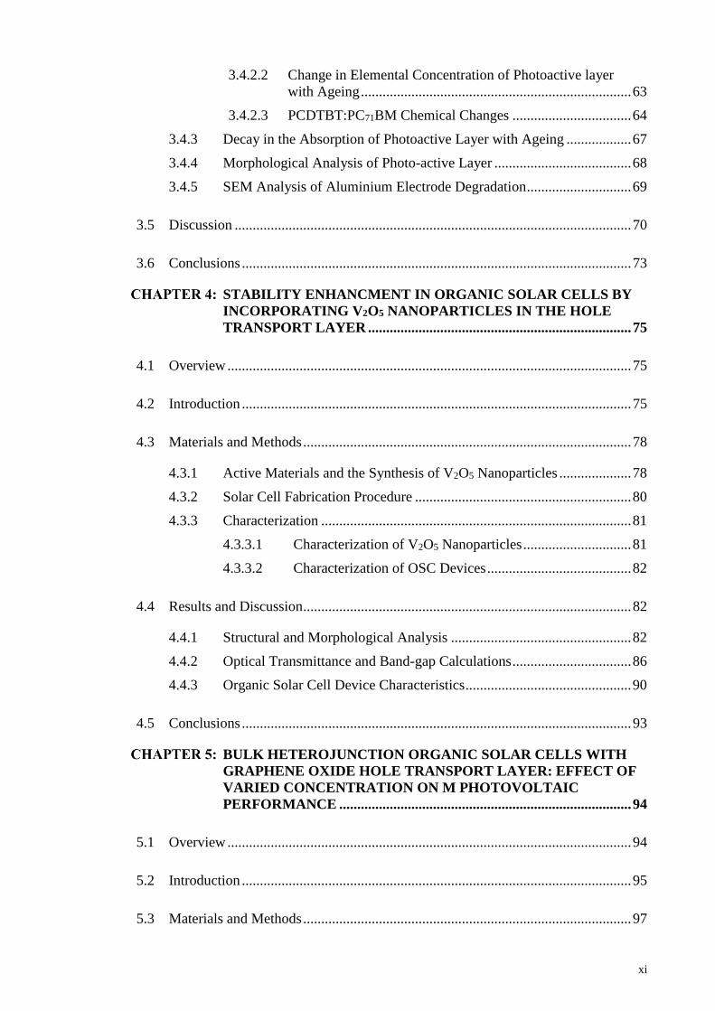
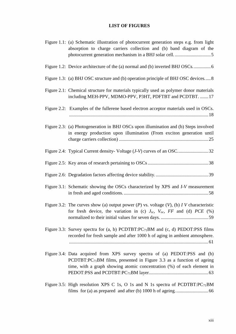
LIST OF FIGURES
Figure 1.1: (a) Schematic illustration of photocurrent generation steps e.g. from light
absorption to charge carriers collection and (b) band diagram of the
photocurrent generation mechanism in a BHJ solar cell. .............................. 5
Figure 1.2: Device architecture of the (a) normal and (b) inverted BHJ OSCs. .............. 6
Figure 1.3: (a) BHJ OSC structure and (b) operation principle of BHJ OSC devices. .... 8
Figure 2.1: Chemical structure for materials typically used as polymer donor materials
including MEH-PPV, MDMO-PPV, P3HT, PDFTBT and PCDTBT. ....... 17
Figure 2.2: Examples of the fullerene based electron acceptor materials used in OSCs.
..................................................................................................................... 18
Figure 2.3: (a) Photogeneration in BHJ OSCs upon illumination and (b) Steps involved
in energy production upon illumination (From exciton generation until
charge carriers collection) ........................................................................... 25
Figure 2.4: Typical Current density- Voltage (J-V) curves of an OSC. ......................... 32
Figure 2.5: Key areas of research pertaining to OSCs ................................................... 38
Figure 2.6: Degradation factors affecting device stability. ............................................ 39
Figure 3.1: Schematic showing the OSCs characterized by XPS and I-V measurement
in fresh and aged conditions. ....................................................................... 58
Figure 3.2: The curves show (a) output power (P) vs. voltage (V), (b) I V characteristic
for fresh device, the variation in (c) Jsc, Voc, FF and (d) PCE (%)
normalized to their initial values for seven days. ........................................ 59
Figure 3.3: Survey spectra for (a, b) PCDTBT:PC71BM and (c, d) PEDOT:PSS films
recorded for fresh sample and after 1000 h of aging in ambient atmosphere.
..................................................................................................................... 61
Figure 3.4: Data acquired from XPS survey spectra of (a) PEDOT:PSS and (b)
PCDTBT:PC71BM films, presented in Figure 3.3 as a function of ageing
time, with a graph showing atomic concentration (%) of each element in
PEDOT:PSS and PCDTBT:PC71BM layer.................................................. 63
Figure 3.5: High resolution XPS C 1s, O 1s and N 1s spectra of PCDTBT:PC71BM
films for (a) as prepared and after (b) 1000 h of ageing. ........................... 66
xiv
Figure 3.6: High resolution XPS spectra for (a) S 2p fresh and (b) In 3d 1000 h aged
sample. ......................................................................................................... 67
Figure 3.7: (a) Evolution of the PCDTBT:PC71BM absorption (300-800 nm) versus
exposure time to ambient air (Fresh - 1000 h), (b) Decay of the normalized
PCDTBT:PC71BM absorption upon exposure in ambient atmosphere. ...... 68
Figure 3.8: SEM and AFM images of PCDTBT:PC71BM films (a, b) Fresh and (c, d)
after 72 h of ageing at ambient atmospheric conditions. ............................. 69
Figure 3.9: FESEM images of Al electrodes for (a, b) as deposited samples and (c, d)
after exposing to the ambient atmosphere for 1000 h. ................................ 70
Figure 4.1: Molecular structures of (a) PCDTBT, (b) PC71BM, and (c) PEDOT:PSS. . 78
Figure 4.2: Flow chart of V2O5 nanoparticles synthesis via hydrothermal method. ...... 79
Figure 4.3: Device structure of PCDTBT:PC71BM solar cells with (a) PEDOT:PSS, (b)
PEDOT:PSS + V2O5 as HTL, and the energy diagram for solar cells with
(c)PEDOT:PSS, and (d) PEDOT:PSS + V2O5 as HTL. .............................. 81
Figure 4.4: (a) XRD pattern of the V2O5 nanoparticles synthesis by hydrothermal
method, (b) Raman spectra of pristine PEDOT:PSS HTL and its hybrid
variant. Inset shows Raman fingerprints for V2O5 nanoparticles and (c) EDS
spectra of synthesized V2O5 nanoparticles .................................................. 84
Figure 4.5: FESEM and AFM images for (a, c) pristine PEDOT:PSS HTL and (b, d)
Hybrid HTL. ................................................................................................ 85
Figure 4.6: The transmittance spectra, for (a) pristine PEDOT:PSS and PEDOT:PSS
enhanced with V2O5 nanoparticles, the Tauc plot of (aE)2 against the photon
energy (E) for (b) freshly prepared HTL variants and (c) aged HTL
variants......................................................................................................... 88
Figure 4.7: The current-voltage (I-V) characteristic in fresh condition, after one week,
and after 4 weeks for OSCs with (a) PEDOT:PSS, and (b)
PEDOT:PSS+V2O5 HTL layer. ................................................................... 91
Figure 4.8: Normalized efficiency (η/ηo) of both OSCs with pristine PEDOT:PSS layer
and PEDOT:PSS + V2O5 nanoparticles layer measured for 28 days (four
weeks). ......................................................................................................... 92
Figure 5.1: (a) Schematic device structure and (b) energy level diagram of the
PCDTBT:PC71BM based devices with GO HTLs of varied concentration.
................................................................................................................... 100
xv
Figure 5.2: (a) Thickness vs concentration plot (b) Raman spectra of GO films,
(c) optical transmittance and (d) series resistance (Rs), at 1, 2 and 4mg/ml
concentration. ............................................................................................ 102
Figure 5.3: AFM topography image and SEM surface scan of GO films at the
concentration of (a) 1 mg/ml (b) 2 mg/ml and (c) 4 mg/ml. ..................... 104
Figure 5.4: (a) Rectification ratio of the OSCs with GO HTL variant and (b) J-V
characteristics of the devices fabricated with GO based HTLs of varied
concentration at 1, 2 and 4 mg/ml. ............................................................ 105
Figure 6.1: (a) Schematic illustration of the BHJ OPVs with GO, PEDOT:PSS and
GO/PEDOT:PSS HTLs and (b) The energy band diagram showing the
energy levels of all the materials used in OPVs of current study. ............. 115
Figure 6.2: (a)Transmittance of GO, PEDOT:PSS and GO/PEDOT:PSS films deposited
on ITO coated substrate and that of bare ITO substrate. (b) Raman spectra
for GO, GO/PEDOT:PSS and (c) PEDOT:PSS HTLs. (d) Deconvoluted
XPS C 1s spectrum of GO. ........................................................................ 117
Figure 6.3: The AFM surface topography images and SEM cross-sectional images with
complete device, of (a, b) GO (c, d) PEDOT:PSS and (e, f)
GO/PEDOT:PSS HTLs. ............................................................................ 119
Figure 6.4: (a) Thickness vs concentration plots for GO. (b) J-V characteristics of OPVs
with GO, PEDOT:PSS and GO/PEDOT:PSS as an HTL. (c) Rsh and Rs
calculated from J-V curves under illumination conditions. (d) Stability test
of OPVs over 250 h. .................................................................................. 122
Figure 6.5: Double logarithmic characteristic (Log V vs. log J) exhibiting effective
charge carrier mobility of PCDTBT:PC71BM based OPVs with GO,
PEDOT:PSS and GO/PEDOT:PSS as the HTLs. ...................................... 124
Figure 6.6: Photovoltaic performance parameters including (a) Jsc , (b) Voc , (c) FF and
(d) PCEs (%) of PCDTBT:PC71BM based OPVs with GO, PEDOT:PSS
and GO/PEDOT:PSS as the HTLs. ........................................................... 125

xvi
LIST OF TABLES
Table 3.1: Photovoltaic performance parameters for the solar cell devices calculated
prior to the device degradation tests and subsequent 7 days. Devices were
measured by global (AM 1.5 G) solar simulator. ......................................... 60
Table 4.1: The variations in transmittance and band gap energy of pristine and hybrid
HTLs due to ageing for one month. .............................................................. 90
Table 5.1: OSCs photovoltaic performance parameters for GO HTL variants of 1, 2 and
4 mg/ml concentration calculated under illumination and their series
resistance(Rs). .............................................................................................. 106
Table 6.1: Device photovoltaic performance characteristics of PCDTBT:PC71BM OPVs
incorporating GO, PEDOT:PSS and GO/PEDOT:PSS as the HTLs. ......... 122
xvii
LIST OF SYMBOLS AND ABBREVIATIONS
AFM : Atomic force microscopy
Al : Aluminium
BHJ : Bulk heterojunction
EDS : Energy dispersive spectra
ETL : Electron transport layer
FESEM : Field emission scanning electron microscopy
FF : Fill factor
GO : Graphene oxide
HOMO : Higher occupied molecular orbital
HTL : Hole transport layer
ITO : Indium tin oxide
I-V : Current-Voltage
Jsc : Short circuit current density
J-V : Current density-Voltage
LUMO : Lower unoccupied molecular orbital
OPV : Organic photovoltaic
OSC : Organic solar cells
PC71BM : (6,6)-phenyl C71 butyric acid methyl ester
PCDTBT :
poly[N-90-heptadecanyl-2,7-carbazole-alt-5,5-(40,70-di-2-thienyl-
20,10,30 benzothiadiazole)]
PCE : Power conversion efficiency
PEDOT:PSS : Poly(3,4-ethylenedioxythiophene) polystyrene sulfonate
PV : Photovoltaic
R2R : Roll to roll
xviii
RMS : Root mean square
RR : Rectification ratio
Rs : Series resistance
Rsh : Shunt resistant
TMO : Transition metal oxide
UV-Vis : Ultraviolet-Visible
V2O5 : Vanadium Pentaoxide
Voc : Open circuit voltage
WF : Work function
XPS : X-ray photoelectron spectroscopy
XRD : X-ray diffraction

1
INTRODUCTION
1.1 Background
In today’s world, the energy regimen is largely reliant on non-renewable and
polluting energy sources, consequently, the global temperature is expected to rise about
1 to 6 °C during the 21st century (Ameri et al., 2009). Conventional energy harvesting is
based on fossil fuels such as oil, gas, and coal which have unsustainable consequences
for environmental, economical, geopolitical and societal issues. Carbon dioxide (CO2)
concentration is expected to rise between 540 to 970 parts per million until 2100 that is
sufficient to cause substantial and irreversible modifications in the global climate
(Ameri et al., 2009; Karl & Trenberth, 2003). Moreover, the energy consumption in
many developed nations is still not at its peak plus there is an increasing demand of
electricity utilization from the developing countries (Conti et al., 2011). According to
the International Energy Outlook 2016, projected increases in world energy
consumption is estimated to reach at 815 quadrillion Btu in 2040 which was 549
quadrillion Btu in 2012, an increase of 48 %. Consequently, a rise in energy
consumption, the depletion of these non-renewable sources and global warming are
causing a severe threat to the balance of human life. Therefore, great attention was
driven towards the clean and renewable energy sources of which solar energy is
believed to have highest potential among other alternative energy resources such as
hydroelectric, biomass and wind energy. There are several reasons of choosing solar
energy as one of the most promising renewable energy resources to fulfill energy
demands of the world. Many areas of developing countries lack grid infrastructures for
transmission of electricity generation. This makes locally generated power potentially
better suited to meet energy demands of these countries. In addition, sun is the most
abundant source of energy on earth and the annual amount of energy received from the

2
sun is enormous; 3.9 ×10²⁰ joules which is enough to meet world energy demand in
less than an hour (Anderson et al., 2004).
Despite of the fact that earth receives abundant solar power, the photovoltaic
(PV) technology is still cost intensive to become a primary energy source. Therefore,
the development of highly efficient, cost effective and industrial scale technology is
required to ensure a bright future of PV products.
1.2 Solar Cell Generations
Solar cells are manufactured through range of technologies including wafer
based and variety of thin film technologies. These technologies are traditionally
grouped into first, second and third generations. Below, a brief description of each
generation is presented.
First Generation (IG): First generation (1G) solar cells are produced on silicon
wafers including single crystal (c-Si) and multi-crystalline silicon (mc-Si) (Bagnall &
Boreland, 2008). Current photovoltaic market is dominated by this generation due to
their high efficiencies typically in the range of 15-25 % (Bagnall & Boreland, 2008;
Green et al., 2015). However, the production of these solar cells require high quality
silicon, state of the art high temperature processing and complex engineering, and are
therefore not a cost effective energy source (Sun & Sariciftci, 2005). In addition, these
solar cells are rigid with less mechanical flexibility.
Second Generation (2G): One of the key challenges in the production of IG
solar cells is their high production cost. Therefore, the second generation (2G) solar
cells were designed with the aim to remove unnecessary material from the cost equation
by using single-junction devices based on thin film technology (Badawy, 2015), while
maintaining the high efficiencies comparable with the 1G solar cells. These 2G devices

3
are fabricated on low cost substrates by using less material based on amorphous silicon
(a-Si), cadmium telluride/sulfide (CdTe/CdS), copper Indium (Gallium) diselenide
(CIS, CIGS) or polycrystalline-Si (p-Si), thereby reducing the overall cost in the
manufacturing process (Green et al., 2006).
Third Generation (3G): The third generation (3G) solar cells are based on
organic small molecules or polymers and designed to complement the advantages of
both 1G and 2G devices (Brown & Wu, 2009). The concept aims to reduce the cost per
watt peak, by maintaining high efficiencies, and economic and environmental cost
advantages of thin-film deposition techniques (Conibeer, 2007). 3G technologies
introduce the idea of multiple stacking of solar cells, which can significantly increase
the efficiency by improving the harvesting of photons and even overcome the
theoretical limit of 30 % (Karam et al., 1999; Zweibel, 2010).
The 3G exhibits an entirely new concept of device architecture and materials i.e.
organic solar cells (OSCs), dye sensitized solar cells (DSSCs) and perovskite solar cells
etc. (Sharma et al., 2015). The polymer solar cells including organic/inorganic hybrid
are fundamentally new types of devices which offer several advantages over their 1G
and 2G counterparts such as their tunable properties, low manufacturing cost, roll to roll
(R2R) production compatibility, solution processed and light weight (Chen et al., 2013;
Sun et al., 2010; Synooka et al., 2014). However, they exhibit significant instability
when exposed to air, mainly due to oxygen and moisture ingress from air, and diffusion
of indium from indium tin oxide (ITO) anode (Krebs et al., 2008; Kawano et al., 2006).
Further improvement in the stability of OSCs is however, essential for most of the
technological applications (Kawano et al., 2006).
This thesis purely focused on modification of hole transport layer (HTL) in the
bulk heterojunction (BHJ) OSCs with polymer-fullerene photoactive layer to improve

4
the stability as well as efficiency of devices. The basic working principle of BHJ OSCs,
device architecture, typical materials, role of interfacial layers and stability/degradation
of OSCs will be discussed briefly in the following sections.
1.3 Bulk-Heterojunction Organic Solar Cells
Since the production of organic photovoltaic materials in mid 1980s, solution
processable OSCs based on thin film technologies have attracted immense attraction as
a possible alternative to their inorganic counterparts (Bulavko & Ishchenko, 2014).
Potential for cost effective and fast R2R production as well as their light weight and
fabrication on flexible substrates could give them an edge over traditional inorganic
solar cells (Scharber & Sariciftci, 2013; Shivanna et al., 2014).
Thanks to the discovery of an ultrafast charge transfer which opened the great
but simple field of so-called BHJ OSCs. To date, remarkable progress in the BHJ OSCs
has been recorded and power conversion efficiencies (PCEs) of more than 10% have
been successfully demonstrated (Li et al., 2012; Trost et al., 2015). The photoactive
layer of a BHJ-OSC is made of a bi-continuous composite of electron-donor and
electron-acceptor modules sandwiched between the cathode and anode (Huang et al.,
2014). The basic structure , operational principal, device geometries and materials have
been briefly discussed below, whereby schematic illustration of BHJ OSCs and
corresponding energy-bands is illustrated in Figure 1.1.

5
Figure 1.1: (a) Schematic illustration of photocurrent generation steps e.g. from light
absorption to charge carriers collection and (b) band diagram of the
photocurrent generation mechanism in a BHJ solar cell.
1.3.1 Device Structure and Materials
A BHJ OSC is essentially consisted of multilayer structure in which each layer
in the device architecture could be deposited by an individual fabrication technique. The
device is illuminated through the transparent substrate, a glass or flexible (plastic)
substrate in most cases, coated with high work function (WF) indium tin oxide (ITO),
the transparent anode that provides the extraction and collection of positive charge
carriers (Huang & Huang, 2014). The cathode is usually made of a low WF opaque
metal such as aluminum (Al) or calcium (Ca) (Po et al., 2011), whereas, the absorber
layer is comprises of two constituents; A donor material is usually a conjugated
polymer, conjugated pigments or oligomers, and for an acceptor material often
fullerene derivatives are applied. The photoactive layer is sandwiched between the
anode and top low WF cathode. In order to improve the performance and stability of the
BHJ OSCs, often interfacial layers namely HTL and electron transport layer (ETL) are
inserted between the anode-photoactive and cathode-photoactive interfaces (Facchetti,

6
2013). Over the years, inverted device architecture has also been established for BHJ
OSCs. In an inverted device, the bottom transparent electrode serves as the cathode
while the top electrode is anode. The performance of inverted devices is comparable
with the normal architecture solar cells; in addition, they also exhibit relatively higher
environmental stability. Typical device architecture for normal and inverted solar cells
is illustrated in Figure 1.2.
Figure 1.2: Device architecture of the (a) normal and (b) inverted BHJ OSCs.
1.3.2 BHJ OSCs Working Principle
The simplified working principle of BHJ OSC device can be described in at least
four fundamental steps namely (i) Photons absorption and exciton formation, (ii)
exciton diffusion and splitting, (iii) charge transportation and (iv) charge collection
(Deibel & Dyakonov, 2010; Dou et al., 2013; Facchetti, 2013).
In a BHJ OSC device, light is usually absorbed in the donor material e.g. a
conjugated polymer. Upon absorption of photons, an electron is excited from the
highest occupied molecular orbital (HOMO) to the lowest unoccupied molecular orbital
(LUMO). The offset between donor (LUMO) and acceptor (LUMO) must be in the
range of 0.1-1.4 eV to generate the electron-hole pairs also known as the excitons. The
7
excitons must diffuse to the donor-acceptor interface where there is sufficient chemical
potential energy drop to split these excitons into the free charge carriers i.e. the
electrons and the holes (Mayer et al., 2007). After splitting into free charge carriers,
each carrier must be transported to the respective electrode through the bi-continuous
interpenetrating pathway while avoiding recombination and trapping of charges. Some
limitations and losses could occur during these steps such as absorption loss due to
spectral mismatch, thermalization loss, insufficient energy required for exciton splitting,
and charge recombination etc. (Siddiki et al., 2010).
Three important parameters determine the PCE of a solar cell: The current that
reaches to the electrodes without any applied field is termed as the short circuit current
(Jsc) whereas open circuit voltage (Voc) is the maximum potential generated by the
device. In order for the current to do work, it must be generated with some potential.
The ratio of maximum obtained power to the product of Jsc and Voc is known as fill
factor (FF) and it defines the quality of the device. PCE is defined as product of these
three parameters divided by input power (Pin) and denoted by sign (η). Mathematically;
𝜂 =𝑃𝑜𝑢𝑡
𝑃𝑖𝑛=
𝐹𝐹(𝑉𝑜𝑐×𝐽𝑠𝑐)
𝑃𝑖𝑛 (1.1)
𝐹𝐹 =𝑉𝑚𝑝𝑝×𝐼𝑚𝑝𝑝
𝑉𝑜𝑐×𝐽𝑠𝑐 (1.2)
Where, Vmpp and Jmpp (eq.1.2) are the voltage and current density at the maximum output
power, respectively. The schematic illustration of the basic structure and working
principle of BHJ OSCs is presented in the Figure 1.3.

8
Figure 1.3: (a) BHJ OSC structure and (b) operation principle of BHJ OSC devices.
1.3.3 Role of Interfacial Layers in OSCs
In BHJ OSCs, each layer of the solar cell architecture significantly influences
the device performance and optimization of every layer is essential to achieve the best
optimum performance. As discussed earlier, in the basic device structure the
photoactive layer is sandwiched between the ITO anode and a low WF metal cathode.
In order to ensure the efficient charge extraction at the respective electrodes, the energy
level structure at the electrodes and photoactive layer interface plays an essential role
(Po et al., 2011; Zheng et al., 2016). The electrodes- active layer interface affects the
phase separation, energy level alignment, and a proper interfacial engineering (insertion
of optimized ETL and HTL between photoactive layer and respective electrodes)
provides good ohmic contacts with minimum resistance and higher charge selectivity to
prevent carriers from reaching to the opposite electrodes (Lian et al., 2014; Steim et al.,
2010). In addition it helps in adjusting the surface energetics and WF, and affects the
formation of gradients within the BHJ (Chueh et al., 2015; Zeng et al., 2015). A detailed
discussion on the developmental history of BHJ OSCs, materials and design parameters,
role of interfacial layers in BHJ OSCs, in particular the HTL in context of this thesis,
device physics, performance characteristics, stability/degradation mechanisms and
strategies to improve device performance will be presented in Chapter 2.

9
1.4 Stability/Degradation of the OSCs
During the recent years, OSCs have evolved in terms of efficiency as well as
stability. Stability of the OSCs is one of the major bottlenecks in their long term
performance. Although, the stability of OSCs has remarkably improved and it was
measured in minutes in earlier days which can sustain now for several thousands of
hours under favorable circumstances. However, still a lot of improvement is needed to
address the factors limiting the stability of OSCs (Jørgensen et al., 2012). Degradation
process comprises a range of complex phenomenon simultaneously in play, of which
many of them are not completely understood yet. The multilayers structure and
interfaces of metal/organic, organic/organic materials significantly influences the
overall performance (Bao et al., 2014). Recent reports on the lifetime stability of OSCs
highlighted two major problems regarding the device stability. Firstly, the extrinsic
stability which requires proper encapsulation of devices to prevent the environmentally
induced degradation mainly caused by oxygen and moisture present in the air (Ecker et
al., 2011; Udum et al., 2014). Secondly, the intrinsic stability which is related to the
materials and interfaces present in the OSCs (Jørgensen et al., 2008; Zeng et al., 2015).
Some of the known factors affecting the device stability are surface morphology of
different layers, diffusion of oxygen from atmosphere, corrosion and diffusion of
indium and tin (from ITO anode), mechanical stress and photo-degradation etc. (Cheng
& Zhan, 2016). Several processes and strategies have been employed in recent years to
address stability issues such as optimization of active layer morphology, interfacial
engineering and utilization of hybrid buffered layers, employing inverted geometry,
using stable electrodes and proper device encapsulation. A detailed overview of the
each of the factors limiting the device stability and possible strategies to increase the
stability of OSCs is presented in Chapter 2.

10
1.5 Project Motivation
During the past few years, significant progress has been recorded in BHJ OSCs
by virtue of their low cost, solution processed and environmental friendly fabrication
processes (Deibel & Dyakonov, 2010; Jagadamma et al., 2014). Considerable
improvement in the device performance has pushed the device efficiency towards the
efficient 10% regime (Dennler et al., 2009; Nelson, 2011). Although, a lot of research
has been carried out on OSCs for their widespread commercialization and large scale
production, but they still have many constraints that prevent them to move beyond the
laboratory. Most of the limiting factors are environmentally induced degradations
caused by oxygen, humidity and intrinsic instability of OSCs materials and interfaces
(Choi et al., 2012; Jong et al., 2000). Since chemical, physical, mechanical and
structural properties of organic semiconductors are very sensitive towards ambient
atmosphere, therefore, the photovoltaic properties of OSCs are quite susceptible to
degradation in ambient environmental conditions (Bekci & Ela, 2012; Jørgensen et al.,
2008). Although, the lifetime of OSCs can be improved by adopting various
encapsulation techniques but this approach would significantly increase the production
cost (Udum et al., 2014). Most of the OSCs which are being fabricated today are tested
under controlled environment without even being exposed to ambient air containing
natural humidity. Hence, for the successful widespread commercialization and large
scale production of OSCs, the stability of OSCs also needs to be improved along with
their efficiency (Savagatrup et al., 2015).
Poly (3.4-ethylenedioxythiophene):Poly (styrenesulfonate) (PEDOT:PSS) is the
most commonly applied HTL in OSCs. However it limits the device performance due to
its highly hygroscopic and acidic nature which causes reliability issues while reducing
the cell life drastically (Schulz et al., 2014). There are several pathways that have been
adopted in order to improve the stability of the interface between photoactive layer and

11
the ITO anode. One of the most reliable methods is to optimize the HTL by introducing
favorable materials along with PEDOT:PSS or to replace it with suitable alternatives.
Materials such as metal oxides and/or graphene oxide (GO) along with PEDOT:PSS to
form an organic-inorganic hybrid HTL are expected to address the stability issues
associated with PEDOT:PSS and compliment the drawbacks of any of the individual
materials. The aim to improve the stability and efficiency of BHJ OSCs by utilizing the
aforementioned hybrid HTLs has become the main motivation of this work.
1.6 Project Goals and Outlines
The title of this dissertation is rather broader and involved a couple of different
tasks that have been accomplished during this work. The work is based on results; some
of which have already been published. The articles comprises of projects of different but
interlinked character with the aim to identify the degradation factors limiting the device
stability in general, particularly, in the context of HTL. Further, to optimize the HTL by
using metal oxides such as vanadium pentaoxide (V2O5), and/or GO along with the
PEDOT:PSS in order to address the reliability issues associated with pristine
PEDOT:PSS HTL and enhance the stability of the device while addressing these
factors. In this context, the attempt to group these tasks in different sections, led to
generation of four chapters (Chapter 3-6) that are presented after introduction and
literature review chapters. In particular, Chapter 3 discusses the stability/ degradation
issues involves in deterioration of device performance. It presents layer by layer
identification of degradation factors affecting the device performance. Several
characterization techniques have been employed in order to record the compositional,
morphological, chemical, optical and photovoltaic decay as a function of aging time in
ambient air. Chapter 4 addresses some of the reliability issues associated with the
instability of the HTL by incorporating V2O5 into the PEDOT:PSS HTL. The resultant
device showed enhanced stability and efficiency as compared to pristine PEDOT:PSS

12
HTL. Chapter 5 and 6 present two small projects that involve the utilization of GO as
an HTL. At first, Chapter 5 describes the optimization of GO concentration to replace
PEDOT:PSS as an HTL. It also identifies the limitation brought by GO as a single HTL
material and suggests the possible improvement which could be brought in the device
performance by using GO along with PEDOT:PSS in a bi-layer structure. Further,
Chapter 6 suggests a novel approach to use GO/PEDOT:PSS HTL in the poly[N-90-
heptadecanyl-2,7-carbazole-alt-5,5-(40,70-di-2-thienyl-20,10,30 benzothiadiazole)]
(PCDTBT), and (6,6)-phenyl C71 butyric acid methyl ester (PC71BM) based device
structure. A set of characterizations confirm the efficacy of this approach and a detailed
study on reproducibility and stability of the resultant device has been presented.
Finally, the conclusion of this work is reported in Chapter 7. Along with presenting the
summary of the project this chapter also includes the future challenges and research
directions.
Four goals have been extracted from the current work that describes the aims of
the present study:
1. To optimize the fabrication parameters in order to develop a facile, solution
processable and cost effective fabrication technique of the polymer solar
cells.
2. To identify the degradation factors and stability concerns particularly
related to HTL in the ITO/PEDOT:PSS/ PCDTBT:PC71BM/ Al device
structure.
3. To evaluate the V2O5 and/or GO along with the PEDOT:PSS as a hybrid
HTL in order to address the reliability issues associated with pristine
PEDOT:PSS HTL.

13
4. To evaluate and improve the operational stability of the fabricated devices
with hybrid HTL.
14
LITERATURE REVIEW1
2.1 Development in BHJ OSCs
Tang in 1986, reported the first successful organic photovoltaic device yielding
a PCE of 1% but with a high FF of 65% in a bi-layer device architecture (Tang, 1986).
Both donor and acceptor materials were deposited by sequential thermal vacuum
sublimation of two small molecules. Six years later in 1992, Sariciftci et al. reported the
ultrafast electron transfer from the donor polymer poly[2-methoxy-5-(2-
ethylhexyloxy)]-1,4-phenylenevinylene (MEH-PPV) to the fullerene (C60), which for
the first time suggested the use of conjugated polymers as donor materials and fullerene
derivatives as acceptor material (Kraabel et al., 1993; Sariciftci et al., 1992). Later, the
concept of BHJ comprises of donor and acceptor materials was introduced to address
the performance constraints associated with the shorter diffusion length in OSCs (Halls
et al., 1995; Yu et al., 1995). BHJ is an intimate blend of donor and acceptor materials
within the photoactive layer with large interfacial areas for efficient charge separation
(Zheng, et al., 2015; Rafique et al., 2016). Due to tremendous progress in optimization
of materials and devices, the BHJ architecture is considered as standard for OSCs.
PCEs of more than 10% have been reported recently, however, this value is still
significantly less than what is required for daily applications (Liu et al., 2015). The
development of BHJ OSCs is rapidly accelerating as a potential green solar energy
technology. OSCs are attractive mainly because of the modifiable structures of their
1 The review presented in this Chapter has been submitted to Elsevier: “Renewable & Sustainable Energy Reviews” as;
Rafique et al. Fundamentals of Bulk Heterojunction Organic Solar Cells: An overview of design parameters, device physics,
performance characteristics, stability/degradation factors and strategies for improvement. Renewable & Sustainable
Energy Reviews. (Manuscript Submitted)
15
organic constituents, flexibility, and compatibility with R2R production (Cao et al.,
2014). Most of the work is focused on improving the device efficiency; however, some
visionary scientists have already paid attention to the stability constraints of the BHJ
OSCs (Cao et al., 2014; Jørgensen et al., 2012; Katz et al., 2006). This literature review
chapter does not cover a huge body of literature on this subject during last few years;
instead, it focuses fundamental concept of BHJ OSCs including device physics of BHJ
OSCs, performance characteristics, working principle, materials, limitations and
possible routes of improving the performance.
2.2 OSCs Materials: Ideal Design Properties
The choice of materials used in OSCs is crucial to the overall performance in
terms of efficiency and stability. This section presents a detailed overview of the
material choice and properties, limitations and possibilities for improvement. Further, it
surveys the materials which have been investigated in recent years and analyses the
specific material (PCDTBT:PC71BM) with reference to the aforementioned desired
properties and also discusses the potential advantages and major limitations of these
materials.
BHJ OSCs employing organic donor and acceptor materials should comply
with several performance characteristics for an efficient photocurrent and photovoltage
generation and are thus as follows (Zheng, et al., 2015; Nelson, 2011):
Optimized absorption features of the OSCs by fine tuning the absorption
characteristics to maximize the visible light absorption.
The width of domains of pure donor or acceptor material should be shorter
than the diffusion length of (< ~10 nm) an exciton, in order for most
photo-generated excitons to dissociate, i.e., the two components should be
sufficiently well mixed.
16
Both phases should form continuous percolating networks that connect the
bulk of the film to the anode and cathode.
The electrodes should be chosen to ensure the high selectivity of charge
carrier extraction and collection i.e. electrons must be collected at one and
holes at the other electrode, in order to provide a direction for the
photocurrent. Such selectivity can be achieved using one high and one low
work function electrode.
2.2.1 Donor and Acceptor Polymers
Several factors determine the efficacy of donor and acceptor materials in BHJ
solar cells architecture. While choosing a donor material, it is important to consider
HOMO and LUMO levels with respect to the acceptor material. Moreover, absorption
range can be broaden by lowering the bandgap, thus polymer can absorb more photons
which will consequently increase the Jsc (Scharber et al., 2006; Su et al., 2012). Most of
the semiconductor polymers are hole conductor and named as electron donor polymers
(Cai et al., 2010). The progress of donor polymers has gone through several phases of
research; as a result four prominent names emerged, namely (i) poly
(phenylenevinylene) (PPV) derivatives such as MEH-PPV (Hou & Guo, 2013; Zhou et
al., 2004), (ii) MDMO-PPV (Zheng, et al., 2015), (iii) poly- (thiophene) derivatives,
mainly P3HT (Wright & Uddin, 2012) and (iv) polyfluorene derivatives like PFDTBT
and PCDTBT (Blouin et al., 2007; Cai et al., 2010). Figure 2.1 shows the structure of
these donor polymers. In addition, the full names of these polymers are:
MEH-PPV: Poly [2-methoxy-5-(2’-ethyl-hexyloxy)-1,4-phenylene vinylene]
P3HT: Poly (3-hexylthiophene-2, 5-diyl).
MDMO-PPV: Poly [2-methoxy-5-(3′, 7′-dimethyloctyloxy)-1, phenylenevinylene]
PFDTBT: Poly [2, 7-(9, 9-bis-(2-octyl)-fluorene)]-alt- [5, 5-(4, 7-di-20-thienyl-2,
1, 3-benzothiadiazole)].

17
PCDTBT: Poly [N-9’-hepta-decanyl-2,7-carbazole-alt-5,5-(4’,7’-di-thienyl-2’1’,3’-
b3nzothiadizaole).
Figure 2.1: Chemical structure for materials typically used as polymer donor materials
including MEH-PPV, MDMO-PPV, P3HT, PDFTBT and PCDTBT.
Since last one decade, P3HT emerged as a prominent semiconductor polymer
due to its self-assembling tendency, improved absorption, higher hole mobility
(Schilinsky et al., 2002; Wright & Uddin, 2012) and its ability to crystallize which
means that the final morphology is controllable by varying process conditions or
subsequent treatments (Quiles et al., 2008). P3HT exhibits a bandgap of ~ 1.9eV which
can be further reduced by enhancing the quinoidal character in the polymer (Roncali,
2007). However, in past few years, PCDTBT emerged as a superior donor polymer as
compared to P3HT due its ultrafast charge carrier generation ability and different charge

18
carrier recombination dynamics (Synooka et al., 2014). Section 2.2.2 presents a brief
description of PCDTBT as a prominent donor polymer.
The conventional OSCs mostly use fullerene derivatives as the electron acceptor
material. The unsubstituted fullerene shows poor solubility which limits its applicability
in the device fabrication; therefore a number of substituents were
introduced onto fullerene to overcome the solubility issues (Hou & Guo, 2013). In this
context, Hummelen et al. demonstrated a feasible approach to synthesize PCBM ([6,6]-
phenyl-C61-butyric acid methyl ester), which have been broadly used as one of the
most successful electron acceptor materials due its excellent photovoltaic properties
(Hummelen et al., 1995). Thereafter, the soluble derivatives of C60 have been
successfully utilized as fullerene derivatives to act as electron acceptor materials. These
so-called fullerene derivatives offer several advantages such as ultrafast charge transfer
mechanism between donor polymers and acceptor fullerenes, high electron mobility and
better phase segregation in the polymer-fullerene blend (Cai et al., 2010). Chemical
structures of some of the famous fullerene based electron acceptor materials are shown
in Figure 2.2.
Figure 2.2: Examples of the fullerene based electron acceptor materials used in OSCs.

19
In recent years, all polymer solar cells which employ polymer donor and
polymer acceptor materials as photoactive layer has received great attention (Facchetti,
2013; Kim et al., 2015) due to their enhanced photo-absorption in the visible range as
compared to fullerene. Consequently, it improves the light harvesting and enables
higher PCEs (Lee et al., 2015; Long et al., 2016; Zhou et al., 2016). Recently, Gao et al.
(Gao et al., 2015) demonstrated the all-polymer solar cells with a PCE of 8.27%. This
shows that polymer donor and polymer acceptor based active layer could dominate the
OSCs field in future.
2.2.2 PCDTBT:PC71BM Blend
Leclerc and co-workers in 2007, synthesized the PCDTBT donor polymer for
the first time (Blouin et al., 2007). Since then PCDTBT is regarded as one of the most
extensively studied donor-acceptor copolymers due to its excellent properties (Synooka
et al., 2014). PCDTBT shows nearly perfect quantum efficiency (Park et al., 2009),
high solubility (Blouin et al., 2007), significantly higher PCEs (Wang et al., 2016),
excellent thermal stability (Cho et al., 2010) and longer operational stability of several
thousand hours (Roesch et al., 2013; Zhang et al., 2016).
Recently, Wang et al. (Wang et al., 2016) reported a PCE of 7.13% by
employing co-additives in PCDTBT:PC71BM based BHJ OSCs. PCDTBT:PC71BM
blend also shows excellent operational stability along with high PCEs. Zhang et al.
demonstrated outdoor stability of PCDTBT:PC71BM based BHJ OSCs for over the
course of an year (Zhang et al., 2016). It was concluded that PCDTBT:PC71BM based
solar cells show relatively good stability in the real operational conditions. Contrary to
P3HT-PCBM based blend, where we need post fabrication annealing for the higher
efficiencies, the PCDTBT based OSCs exhibit best performance with un-annealed state,
thus reducing processing steps as compared to P3HT based devices (Synooka et al.,
2014).

20
The main focus of this thesis is to optimize the HTL by using metal oxides
(V2O5) and GO along with PEDOT:PSS to address the stability issues associated with
conventional PEDOT:PSS while maintaining the efficiencies comparable with the
device containing pristine PEDOT:PSS, therefore section 2.2.3 below presents a brief
description of it.
2.2.3 The Buffered Layers
A typical OSC architecture consists of a BHJ photoactive layer sandwiched
between the two electrodes. However, this basic architecture possesses several
performance constraints including lack of ohmic contacts, inefficient charge extraction
and transportation, lack of selectivity in charge collection and mismatch of WF etc.
(Chen et al., 2012). To overcome these issues, OSCs usually include functional layers
(namely HTL and ETL) at the active layer/electrodes interface (Po et al., 2011). The
buffered layers are considered to be critically essential part of the device architecture for
achieving high efficiency and stability in OSCs and can no more be considered as
“optional”. These layers can be used to “engineer” the interface between the photoactive
layer and electrodes which strongly affect this interface by inducing geometry
modifications, chemical reactions and charge redistribution etc. (Ma et al., 2010). These
layers are mainly selected on the merits of their charge transport properties, their energy
levels and offer several potential advantages such as (Cao et al., 2016; Steim et al.,
2010);
i. Buffered layers enable the high selectivity of charge carriers from the
photoactive layer towards the electrodes.
ii. In some cases, they enhance the light absorption leading to higher PCEs,
thus playing the role of an “optical spacer”
iii. Limit the reaction between the photoactive layer and the electrodes.
21
iv. Reduce the energy barriers due to mismatch in the energy levels of
photoactive layer and electrodes.
Anode buffered layer: Since the discussion of ETL is out of this thesis scope,
therefore, a brief description of HTL would only be presented here. The primary role of
HTL is to improve the collection and extraction of positive charge carriers. In addition,
it should block the negative charge carriers to the anode, thus needing a high WF
material. ITO is the most commonly used anode electrode and its WF (~ 4.7 eV) does
not match either with the HOMO level of most of the donor polymers or with the
LUMO of fullerene based acceptor, thus, leading to a large band offset which results in
recombination of charge carriers at the interface (Kettle et al., 2012). Therefore, use of
PEDOT:PSS as state of the art HTL enables the high WF and planarize the
electrode/active layer interface (Bailo et al., 2012). In addition, it also offers high
conductivity and transparency and helps in adjusting surface defects passivation
(Ameen et al., 2015). On the other hand, it is also true that PEDOT:PSS favors the
device degradation due to its highly acidic and hygroscopic properties, leading to
indium corrosion and oxygen ingress, respectively Shrotriya et al., 2006).
To date, the known HTL materials are transition metal oxides (TMOs) (Chen et
al., 2012; Shrotriya et al., 2006), conjugated or non-conjugated polymers (He et al.,
2014), small molecule organic materials, self-assembled monolayers (Zhao et al., 2015)
and GO (Jeon et al., 2014; Liu et al., 2013). These materials have been reported to either
replace PEDOT:PSS or used along with PEDOT:PSS to overcome stability issues
associated with pristine PEDOT:PSS HTL. Among the HTL materials used in OSCs,
TMOs are promising candidates due to their better environmental stability, high
transparency and comparable device performance with that of PEDOT:PSS (Chen et al.,
2012; Choi et al., 2015).
22
The very first use of TMOs in the field of organic electronics can be traced back
in 1996 when Tokito et al. used vanadium oxide (VOx), molybdenum oxide (MoOx) and
ruthenium oxide (RuOx) as HTLs in organic light emitting diodes (OLEDs) (Tokito et
al., 1996). In the pursuit for overcoming the stability concerns pertaining to
PEDOT:PSS, researchers have identified several TMOs such as V2O5 (Chen et al.,
2011; Cho et al., 2015), tungsten oxide (WO3) (Li et al., 2012; Stubhan et al., 2012),
molybdenum oxide (MoO3) (Lee et al., 2012; Murase & Yang, 2012) and nickel oxide
(NiOx) (Hsu et al., 2015; Manders et al., 2013) to serve as HTLs in OSCs. It has been
reported that certain metal oxides can act as an optical spacer (Gershon, 2011),
moreover, TMOs are chemically and mechanically stable during their interaction with
the organic photoactive layer, thus minimizing any undesired chemical reactions and
increasing device life time (Ma et al., 2010 ). In addition, these metal oxides have high
WFs so their Fermi levels match well with the HOMO level of photoactive polymer and
they help to decrease the energy level offset between the photoactive layer and the ITO
anode.
In the current work, V2O5 and GO have been employed as an HTL material
along with the PEDOT:PSS to form a hybrid HTL in the PCDTBT:PC71BM normal
architecture solar cells. Therefore, a short description of each of these two materials is
presented below.
2.2.3.1 V2O5 as an HTL Material
Metal oxide V2O5 has been widely explored as an HTL in BHJ OSCs. It can form an
efficient HTL junction with the photoactive layer due to its much higher conduction
level than the lowest occupied molecular orbital (LOMO) of the organic photoactive
layer which can effectively block the undesired transportation of electrons towards the
electrodes and thus, performance of the device can be significantly enhanced (Pan et al.,

23
2016). In addition, it shows very good transparency in visible region, wide optical
bandgap, good interfacial adhesion and better environmental stability (Meyer et al.,
2011; Rafique et al., 2016; Zilberberg et al., 2011). At initial stage of TMO based
OSCs, metal oxides were usually deposited by cost intensive vacuum based processes
(Kyaw et al., 2008). However, in recent years several reports confirm the efficacy of
solution processable V2O5 HTL in BHJ OSCs device architecture showing high stability
and efficiency (Rafique et al., 2016; Escobar et al., 2013; Wang et al., 2012). The
reported work related to V2O5 as an HTL can be classified into two categories: one is
using V2O5 as an HTL to replace PEDOT:PSS; the other is to use V2O5 along with
PEDOT:PSS to form an organic-inorganic hybrid HTL. The latter option has been
adopted to compliment the best features of both of the materials while overcoming their
disadvantages. In this context, J. Pan et al. recently reported PEDOT:PSS/V2O5 double
decked HTL by depositing V2O5 nanowires on top of the PEDOT:PSS layer (Pan et al.,
2016). The resultant device outperformed the devices fabricated with either of
individual materials on merits of their performance. In our recently reported work, V2O5
nanoparticles were dispersed in PEDOT:PSS aqueous suspension and the resultant
device showed enhanced stability as compared to the device with that of pristine
PEDOT:PSS (Rafique et al., 2016). It is thus concluded that solution processable V2O5
based HTL could be a simple and facile route to fabricate BHJ OSCs with high
efficiency and stability.
2.2.3.2 GO as an HTL Material
It is obvious that development of facile, solution processable and low cost HTL
material compatible with OSC materials is urgently demanded in recent years. In this
context, solution processed GO derivatives have emerged as an efficient HTL material
for OSCs with long term stability (Li et al., 2010; Liu et al., 2012). In particular, spin
coated GO is regarded as a promising alternative to pristine PEDOT:PSS HTL due to its

24
easy fabrication approach, excellent transparency, mechanical flexibility and R2R
production compatibility (Kim et al., 2013; Stratakis et al., 2014; Stratakis et al., 2013).
GO is a derivative of graphene, consisting of one atomic layer thick graphene sheet
functionalized with hydroxyl (OH) and epoxy groups on the basal planes and carboxylic
groups (COOH) at the edge (Cheng et al., 2015; Ding et al., 2015). It contains a mix of
sp2 and sp3 hybridized carbon atoms and, especially, sp2 hybridized domain of GO
provides opportunities to tailor its optoelectronics characteristics (Li et al., 2010; Yang
et al., 2012). Although, GO possesses insulating properties, however, it still can
facilitate the transportation of holes via hoping (Dehsari et al., 2014). Moreover, the GO
based device possess excellent device stability as compared to the one with
PEDOT:PSS HTL (Yusoff et al., 2014). GO is water soluble and could be combined
with different organic and inorganic materials. It also retains the high transparency and
its WF (4.9 eV, lower than PEDOT:PSS which is 5.1 eV) is comparable to PEDOT:PSS
(Smith et al., 2014). However, GO as an HTL material also possesses some drawbacks
including its insulating properties leading to poor Ohmic contacts, poor film uniformity
and relatively low WF as compared to PEDOT:PSS (Ding et al., 2015). Therefore, a
GO/PEDOT;PSS composite layer is expected to overcome these issues associated with
either of the single material. It is reported that an ultrathin layer of GO underneath the
PEDOT:PSS could act as a barrier against the ITO diffusion and acid corrosion, and
also facilitates the extraction of holes via hoping due to well matched WF between GO
and PEDOT:PSS as well as GO can effectively block the undesired flow of electrons
due its large bandgap (~ 3.6 eV) (Dehsari et al., 2014). Moreover, the GO/PEDOT:PSS
composite HTL shows better electrical conductivity, higher PCEs and enhanced
stability (Yu et al., 2014).

25
2.3 Device Physics of BHJ OSCs
Since the development of BHJ device structure based on conjugated polymers-
fullerene based intimated blend, this material combination has led to several
breakthroughs in efficiencies with PCEs approaching above 10% regime (Chen et al.,
2014). In addition, the stability of the OSCs has also substantially enhanced while
device life of several thousand years has already been reported in real operational
conditions (Zhang et al., 2016). This section reviews the process and performance
characteristics that govern device operation of polymer-fullerene BHJ OSCs. The
schematic representation of operating principle of OSCs is illustrated in Figure 2.3.
Figure 2.3: (a) Photogeneration in BHJ OSCs upon illumination and (b) Steps
involved in energy production upon illumination (From exciton generation
until charge carriers collection)
2.3.1 Light Absorption and Exciton Generation
To achieve the high efficiency, the photoactive layer must absorb the maximum
of the incoming sunlight. Light is usually absorbed by donor fraction of the BHJ
26
photoactive layer. Due to high absorption co-efficient of conjugated polymers
(107 m−1) , they can effectively absorb light at maximum of their absorption spectrum
(Blom et al., 2007) with very low thickness of the photoactive (100-200 nm) layer as
compared to their in-organic silicon (an indirect semiconductor) based counterparts
where thicknesses of hundreds of micrometers are required. Thus, the OSCs employing
conjugated polymers significantly lower the amount of material. Unfortunately, owing
to the narrow band of conjugated polymers as compared to inorganic semiconductor,
they typically cover the small region of the solar spectrum only, thus, showing poor
performance than inorganic solar cells (Hoppe et al., 2003; Lioudakis et al., 2007; Peet
et al., 2007). Moreover, the thickness of polymer based photoactive layer is also limited
to 100 nm due to low charge-carrier mobilities in most of the polymers which leads to
an absorption of only 60% of the incident light at the absorption maximum (excluding
back reflection of the electrode) (Blom et al., 2007). In contrast, the inorganic
semiconductors can effectively absorb the whole visible solar spectrum (Blom et al.,
2007; Deibel & Dyakonov, 2010). Thus, low absorption in conjugated polymers leads to
low photocurrent generation. Interestingly, the absorption of light can be enhanced by
lowering the bandgap of donor polymers which results in absorption of maximum
number of photons that lead to higher PCEs (Brabec et al., 2002; Yeh & Yeh, 2013).
Therefore, materials with lower bandgap are necessary to optimize the photon
harvesting. Generally, a material with bandgap lower than 2 eV is considered as a low
bandgap material that lead to the possibilities of improving the efficiency of OSCs due
to a better overlap with the solar spectrum. For example, a bandgap of 1.1 eV can cover
77% of the AM 1.5 solar photon flux as compared to bandgap of 1.9 eV that can hardly
cover 30 % of the AM1.5 photon flux (Yeh & Yeh, 2013). Thus, a low bandgap
material can significantly improve the photocurrent generation.

27
Luckily, the bandgap of conjugated polymers can be lowered down to even 0.5
eV through numerous manipulations and modifications of their chemical structures
(Jean Roncali, 1997). A simple rule of thumb to lower the bandgap is to either raise the
LUMO or lower the HOMO levels of the polymer or bring them together
simultaneously (Cheng et al., 2009). Several methods have been adopted to enhance the
absorption range of donor polymers such as extending the conjugation length of the π-
conjugated segments (Mühlbacher et al., 2006). In general, conjugation length is in
inverse proportion to the difference between the HOMO and
LUMO of the conjugated polymers. However, after certain extension in conjugated
length it reaches to a saturation point and the bandgap starts to level off. Thus, an
unlimited extension of the conjugation length results only in a limited reduction of the
bandgap (Cheng et al., 2009). Another widely used approach is to combine electron rich
and electron poor units in the polymer backbone in a ‘push-pull’ structure i.e.
combining the thiophene containing (electron rich) and benzothiadiazole [BT] (electron
poor). In this approach, the HOMO of the copolymer is dominated by the HOMO of the
electron deficient unit and the LUMO by that of the electron rich unit. A remarkable
improvement in the PCEs of OSCs has been made by using the so-called push-pull
copolymers (Bronstein et al., 2011; Mühlbacher et al., 2006; Peet et al., 2007).
Light is illuminated from the transparent electrode side, and on absorption of
photon; an electron is excited from the HOMO to the LUMO. It is similar to inorganic
semiconductors where electron is excited from valence band to the conduction band. As
a result an electron-hole pair (exciton) with binding energy typically in the range of 0.1–
1.4 eV is generated (Mayer et al., 2007). Contrary to inorganic semiconductors, higher
binding energy in organic materials is due to strong coulomb’s attractions between the
electron–hole pairs. The excitons are then migrated to donor-acceptor interface. A
schematic representation of steps in energy production is shown in Figure 2.3.

28
2.3.2 Exciton Diffusion and Charge Dissociation
Singlet excitons in organic semiconductor materials migrate between conjugated
segments through Förster energy transfer (Scheidler et al., 1996). Owing to the
disordered nature of the polymers such hopping is referred as diffusion (Mikhnenko et
al., 2014). These coulombically bound electron−hole pairs cannot generate photocurrent
and for photovoltaic applications, BHJ of electron donor and electron acceptor is used
to generate charge carriers. Further, the energy offset in LUMO between donor and
acceptor materials breaks the Coulomb attraction which ultimately causes the excitons
to dissociate (Dimitrov & Durrant, 2013; Gao & Inganäs, 2014; Ohkita & Ito, 2013).
Therefore, excitons must diffuse into the donor-acceptor interface to dissociate into
charge carriers before deactivating to the ground state (Tamai et al., 2015). However,
the thermal energy at room temperature which is required to dissociate an exciton into
free charge carriers is not enough due to the high exciton binding energy in conjugated
polymers (Blom et al., 2007).
As most of the conjugated polymers exhibit shorter lifetime of the excitons, the
diffusion lengths are limited to a few nanometers (less than 20 nm), which is much
shorter than the optical absorption pass length (∼100−200 nm). As a result, the PCE of
a bi-layer cell is limited by the low number of photons that can be absorbed within the
effective exciton range (Markov et al., 2005). To circumvent this issue, the BHJ
structure has been widely adopted to maximize the harvesting of excitons at the
interface (Kang et al., 2016; Yu & Heeger, 1995). However, it is the prerequisite that
excitons must be generated within their diffusion length (LD) for efficient charge
generation (Scharber & Sariciftci, 2013). Exciton diffusion length is defined as the
distance travelled by an exciton before recombination (Fung & Choy, 2013). The
reported excitons diffusion length for various conjugated polymers significantly varies
ranging from 5 to 20 nm (Halls et al., 1996; Haugeneder et al., 1999; Stübinger &

29
Brütting, 2001). Thus, the thickness of the photoactive layer is very much critical for an
efficient charge generation. However, a thin layer of photoactive BHJ material has to
compromise on low absorption efficiency. Therefore, large interface area for exciton
splitting and optimum phase separation is highly desirable which results in efficient
exciton dissociation (Fung & Choy, 2013).
In organic semiconductors, photogenerated holes and electrons at the
donor/acceptor interface experience a strong Coulomb binding energy (Clarke &
Durrant, 2010; Deibel et al., 2010). These Coulomb bound electron–hole pairs have to
be dissociated to get free charge carriers. However, they either recombine or dissociate
into free charge carriers upon escaping their mutual Coulomb attraction (Blom et al.,
2007; Deibel & Dyakonov, 2010). Efficient charge transportation requires efficient
dissociation of excitons at the interface. The difference in HOMO and LUMO between
donor and acceptor layers creates electrostatic forces at the interface. When materials
choice is proper, such differences generate electric field that leads to the efficient break
up of excitons into electrons and holes (Yeh & Yeh, 2013). Further, the free electrons
are then accepted by the material with higher LUMO level and holes by the material
with lower HOMO. Unfortunately, these free charge carriers can lead to recombination
or trapping in a disordered interpenetrating organic material while travelling towards the
electrodes.
2.3.3 Free Charge Carrier Transport
After the exciton dissociation into free charge carriers, the charges should be
transported towards the respective electrodes as shown in Figure 2.3. The transportation
of charge carriers in organic semiconductors mostly takes place by hopping from one
localized state to the next (Baranovskii et al., 2000; Pivrikas et al., 2007). Moreover, in
the BHJ of donor- acceptor materials, the donor is generally a hole conductor and an

30
acceptor transports the electrons. Transportation of free charges towards their respective
electrodes is driven by an internal electric field occurred due to the Fermi level
difference of the electrodes (Zhou et al., 2010). In general, a high WF anode and a low
WF cathode create an internal electric field that determines the Voc of the cell (Fung &
Choy, 2013). Transportation of free charge carriers is either driven by the carrier
diffusion or electric field induced drift.
The main bottleneck to the efficient transportation of free charge carriers
towards the anode and cathode is their recombination before reaching to their respective
electrodes. The charge carrier mobility in the photoactive layer governs both the carrier
transportation as well as the losses caused due to carrier recombination (Mandoc et al.,
2007). In the case of low mobility materials, electrons and holes remain bound by the
Coulomb potential, as a result they cannot overcome their mutual attraction and finally
recombine prior to charge collection at the electrodes (Pivrikas et al., 2007).
Consequently, the solar cell experiences a significant loss in terms of photogenerated
current. As discussed earlier, because of low carrier mobility in BHJ materials, the
thickness of the photoactive layer is restricted to less than 100 nm for an optimized
performance (Park et al., 2009). The path length of photogenerated electrons and holes
is in direct proportion to the thickness of the photoactive layer (Cowan et al., 2012).
Charge carrier recombination increases as the photoactive layer gets thicker, resulting in
a substantial loss in the device performance (Lenes et al., 2006). Thus, competition
between carrier sweep-out by the internal field and the loss of photogenerated carriers
by recombination are the important issues to overcome for high efficiency devices
(Cowan et al., 2012).
31
2.3.4 Collection of the Charge Carriers at the Electrodes
Photogenerated charge carriers that do not recombine are finally extracted from
the photoactive layer to the respective electrodes. The potential barrier at the
photoactive layer/ electrodes interface must be reduced to maximize the extraction of
charges (Deibel & Dyakonov, 2010). Therefore, the WF of the anode should match with
the HOMO of the donor material, while the WF of the cathode must match with the
LUMO of the acceptor material (Fung & Choy, 2013). If the WF matches well as
described then the contacts are said to be Ohmic contacts. Contrary to this, if there is a
mismatch between the anode and cathode with that of donor HOMO or acceptor
LUMO, respectively, then no Ohmic contacts would be established. Ultimately, the
performance of the solar cells will decrease (Blom et al., 2007).
The charge collection at the respective electrodes concludes the steps from
absorption of light to generation of photocurrent as show in Figure 2.3. The PV
performance characteristics such as Jsc, Voc and FF etc. are reliant on the photocurrent
generation. Therefore, a brief discussion on the performance characteristics of an OSC
is presented in section 2.3.5.
2.3.5 Performance Characteristics
At present, BHJ OSCs are one of the most successful device architectures in
OSCs, which employ an intimate blend of donor and acceptor materials incorporated in
photoactive layer. In addition, OSCs have the lowest energy payback time (~ 0.4 years)
than silicon (~2.4 years for c-Si) and CdTe (~ 0.7 years) (Peet et al., 2007). To achieve
an optimum performance, a basic understanding of the performance characteristics that
govern the operation of solar cells is necessary that can serve as a guideline to identify
and develop new materials for highly efficient devices.

32
As discussed briefly in Chapter 1, the PCE of an OSC is reliant on the Voc, Jsc,
FF, and Pin defined by the equation 1.1 in Chapter 1. Figure 2.4 shows a typical
Current density - Voltage (JV) curve for a solar cell. It illustrates the critical parameters
which determine the PCE of an OSC. These include the Voc, Jsc, FF, and the values for
JMpp and VMpp (JMpp and VMpp are the points on the J-V curve where maximum power is
produced). The outlined shaded area in the graph indicates the FF whereas, the product
of current and voltage has the highest yield at the maximum power point (MPP)
(Hoppea & Sariciftci, 2004).
Figure 2.4: Typical Current density- Voltage (J-V) curves of an OSC.
Rigorous research has been carried out to optimize these parameters in order to
enhance PCEs of OSCs. Below, a brief description for each of them is presented.
2.3.5.1 Short Circuit Current Density (Jsc)
The Jsc is the maximum photocurrent density generated at zero applied potential
(e.g. short circuit conditions when Voc = 0) (Troshin et al., 2008). Although, there is no
power produced at this point, however, the Jsc marks the onset of the power generation.

33
It is essential parameter which can be affected due to several factors such as locally
enhanced surface recombination, due to regions of low charge carrier lifetimes,
inhomogeneous optical characteristics as well as distances to the metal contacts during
the production process (Padilla et al., 2014). Jsc represents the number of charge carriers
generated and finally collected at the respective electrodes at zero applied potential
(Fung & Choy, 2013). Although it is technically a negative number, but conventionally
its magnitude is considered and treated as a positive number, e.g. a higher Jsc is desired
for higher efficiency.
The performance of an OSC is largely governed by the incident photon to
converted electron (IPCE) efficiency, defined as the externally measured number of
collected charge carriers verses the number of incident photons, and also referred as
external quantum efficiency (EQE) (Armin et al., 2014; Chen et al., 2013). The Jsc is
directly related to the EQE and the relationship between the Jsc and EQE is expressed as
(Wright & Uddin, 2012):
𝐽𝑠𝑐 =𝑞
ℎ𝑐∫ 𝐸𝑄𝐸
𝜆𝑚𝑎𝑥
𝜆𝑚𝑖𝑛× 𝑃𝑖𝑛 (𝜆)𝜆 × 𝑑𝜆……………. (2.1)
Where, q is the charge of electron, λ [nm] is the wavelength of incident photons
and Pin [W/m2] is the incident power. Moreover, IPCE can also be understood as how
efficiently the device converts the incident light into electrical energy at a certain
wavelength (Günes et al., 2007). Mathematically the IPCE it expressed as:
𝐼𝑃𝐶𝐸 =1240𝐼𝑠𝑐
𝜆𝑃𝑖𝑛 ………………….. (2.2)
Where, Isc is the photo-current [µA/cm2], λ [nm] is the wavelength of incident
photons and Pin [W/m2] is the incident power.

34
2.3.5.2 Open Circuit Voltage (Voc)
One of the most important factors determining the device efficiency is Voc which
is determined when J = 0 or it is being open circuited (Chandrasekaran et al., 2011). It is
the measure of the maximum of voltage that a solar cell can extract for an external
circuit (Elumalai & Uddin, 2016; Qi & Wang, 2012). Although, a generally acceptable
view is that Voc in the BHJ OSCs originates from the energy offset between the HOMO
of the donor and LUMO of the acceptor material (Ke et al., 2015), however, early
studies reveals that the Voc is determined by the difference in the WFs of the two
electrodes (Lo et al., 2010), the so called metal-insulator-metal (MIM) model (Günes et
al., 2007; Mihailetchi et al., 2003). Brabec et al. fabricated series of devices with several
fullerenes of varied LUMO level and commonly used donor materials, and reported that
Voc is directly related to the acceptor strength of the fullerenes. Moreover, their results
fully support the view that Voc is reliant on offset between the HOMO level of the donor
and the LUMO level of the acceptor components (Brabec et al., 2001). Scharber et al.
reported in their work that MIM model is not valid for BHJ OSCs and Voc of a BHJ
OSC linearly changes with the energy level offset between the HOMO of donor and
LUMO of the acceptor (Scharber et al., 2006). From their analysis, a simple empirical
equation was proposed to express Voc as:
𝑉𝑜𝑐 = (1 𝑞⁄ )(|𝐸𝐻𝑂𝑀𝑂,𝐷| − |𝐸𝐿𝑈𝑀𝑂,𝐴|) − 0.3𝑉………… (2.3)
Here q is the elementary charge, (EHOMO, D) and (ELUMO, A) are the energy levels
of donor HOMO and acceptor LUMO, respectively. It is noteworthy that 0.3V loss is
empirical, and could be less or more (Qi & Wang, 2012). However, the origin of Voc is
not clear and its variations cannot be fully included from the above rules, thus,
indicating that its origin still needs to be further investigated for better understanding on
OSCs.
35
It is discussed by Widmer et al. (Widmer et al., 2013) in their recent study on Voc
of an OSC that Voc of an OSC is also restricted by the donor-acceptor material system.
Moreover, the nano-morphology of the BHJ photoactive layer also affects the device
performance (Liu et al., 2001). In addition, charge carrier recombination (generally non-
geminate recombination in OSCs) (Groves & Greenham, 2008; Shuttle et al., 2008))
potentially brings the significant loss in the Voc of a device (Qi & Wang, 2012). There
are several factors which can potentially reduce the Voc of an OSC such as temperature,
light intensity, WF of electrodes and material microstructure etc. (Qi & Wang, 2012).
The Voc of the device can potentially be improved by employing interfacial engineering
at the active layer/ electrodes interface such as introducing HTLs and ETLs in the
device structure (Lieuwma et al., 2003). The HTLs and ETLs can effectively reduce the
surface recombination at the electrode/photoactive layer interface (Qi & Wang, 2012).
The Voc is proportional to the built-in potential of an OSC, and by enhancing it will
obviously increase the Voc.
2.3.5.3 Fill Factor (FF)
The FF is an important parameter that determines the PCE of an OSC. The PCE
of an OSC is calculated from its J-V characteristics as a product of Jsc, Voc and FF.
Moreover, the shape of the J-V characteristics of an OSC is characterized by the FF that
is the ratio of the maximum output power to the product of Isc and Voc (Trukhanov et al.,
2015). The shape of the J-V curve determines how ‘‘difficult’’ or how ‘‘easy’’ the
photogenerated carriers can be extracted out of a solar cell device and ideally FF should
be 100% when the J-V curve is exactly a rectangle (Qi & Wang, 2013). In the Figure
2.4, the shaded area represents the FF whereas the representative equation to express FF
has been presented in equation 1.2 of Chapter 1.

36
It is noteworthy that FF is more sensitive parameters as compared to Voc and Jsc
and depends upon several factors such as charge carrier mobility, thickness of the
photoactive layer, morphology of cathode/photoactive layer interface and bulk material
properties (Gupta et al., 2010). Moreover, series resistance Rs is one of the most
important factors affecting FF of an OSC (Kim et al., 2009). In general, a low Rs is
highly desirable that can be achieved with optimized surface morphology, and
consequently a much higher FF is possible to achieve (Kim et al., 2009; Street et al.,
2011). A fraction of increase in Rs can reduce high percentage of FF e.g. for every 0.1Ω
increase in Rs value can reduce 2.5% of FF (Lindmayer & Allison, 1990). The Rs (often
referred as the internal resistance) is comprises of several factors such as active layer
resistance, interfacial layer resistance, electrode resistance, contact resistance of every
interface in the device and probe resistance. Consequently, all these factors have
adverse effects on the FF of a solar cell device (Servaites et al., 2010).
Shunt resistant (Rsh) represents the current leakages in a solar cell including
leakage from edges, pinholes, traps and films etc. An ideal device should not have any
current leakage which implies that ideally Rsh should approach to infinity. Several
factors influence the Rsh of a device and ultimately lower the FF. Kim et al. reported
effective design variables to control FF; their study concluded that most prominent
factors affecting Rsh of a device are the electrode/photoactive layer interface,
illumination intensity and thickness of the blend layer and ultimately, lower the FF
(Kim et al., 2009). By optimizing the aforementioned characteristics of an OSC
including film morphology, interfacial optimization, lower Rs and high Rsh etc., higher
FF values are possible to achieve.

37
2.3.5.4 Power Conversion Efficiency (PCE)
Finally, the most discussed performance parameter of a solar cell device is its
PCE. It is defined as the percentage of input irradiation (Pin) that is converted into the
output power and expressed as the product of Voc, Jsc, and FF divided by the input
power (Pin).
In summary, these key performance parameters of OSCs play an important role
in determining and optimizing the performance of solar cells. To achieve the best
optimum performance, every single factor contributing towards the efficiency of the
device has to be enhanced by improving electrodes, BHJ material, every layer and
interfaces etc.
2.4 Stability of OSCs/Degradation Factors Limiting the Device Stability
OSCs have exponentially evolved in terms of efficiency and stability. While, the
PCE has been increased by almost a factor of ten exceeding 10%, lifetime of the OSCs
has also approached several thousand hours under favorable circumstances (Gevorgyan
et al., 2013; Jørgensen et al., 2012). However, stability is still a bottleneck to the
widespread commercialization of OSCs. While promising achievements in the PCEs of
OSCs, above 10% value only represents the initial performance of the OSCs-how the
PCE of the solar cell degrades with time is also of critical importance. The energy
output of a solar cell device is the product of its efficiency and lifetime stability,
illustrated in Figure 2.5. Therefore device stability is of paramount importance in OSCs
and inferior device stability still remains a great challenge to compete the inorganic
silicon based solar cells in photovoltaic industry. Moreover, the fabrication techniques
must be compatible with the R2R production for the widespread commercialization of
OSCs.

38
Figure 2.5: Key areas of research pertaining to OSCs
Studying the stability of OSCs helps in understanding how a device degrades
during operation. Device instability occurs due to range of complex phenomena that are
in play simultaneously of which presumably many have not been identified (Rafique et
al., 2017). OSCs are highly sensitive to even small degree of degradations which make
degradation factors extremely critical for device operation and thus should be
completely removed or at least reduced to improve device lifetime (Krebs et al., 2010).
Obtaining longer operational lifetime in OSCs is generally challenging, even
though lifetime of several thousand hours has been reported in certain conditions.
Degradation mechanism in OSCs is rather complex and cannot be explained by a single
process. It may include factors affecting active layer, the transport layers, the contacts
and the interface of every layer with the adjacent layers (Guerrero et al., 2012; Kim et
al., 2009). In general, degradation factors in OSCs can be distinguished to be either
intrinsic or extrinsic. Among these factors are oxygen and water diffusion (Norrman et
al., 2008), electro-migration induced shunts, oxidation and rusting of Al electrode due
to moisture (Glen et al., 2015), indium diffusion from anode due to acidic PEDOT:PSS
(Ecker et al., 2011), swelling of water-soluble layers as well as corrosion and

39
delamination of the metal contacts due to oxygen and water ingress (Jørgensen et al.,
2008). Moreover, thermal and photo-induced degradation of active layers under
illumination in ambient conditions, active layer intrinsic chemical evolution, photo-
bleaching and mechanically induced stress also occur in OSCs (Bao et al., 2014;
Guerrero et al., 2015; Morse et al., 2015). Both types of degradation are mass-flow
(diffusion) processes. This section briefly covers some of the most pronounced
degradation effects, while schematic representation of some of the degradation factors
limiting the device stability is shown in Figure 2.6.
Figure 2.6: Degradation factors affecting device stability.
2.4.1 Intrinsic Degradation
OSCs are currently the ultimate in terms of complexity and they exhibit the most
uncontrollable situation in terms of stability. So far, most of the research is focused on
effects of extrinsic degradation factors such as temperature, light, oxygen and humidity
on photoactive layer, electrodes and interfaces. However, less attention has been given

40
to the intrinsic degradation mechanisms. In general, the intrinsic degradation arise from
thermal diffusion of constituent materials at interfaces of OSCs (Cao et al., 2014). Even
after encapsulation (to avoid oxygen and moisture ingress), intrinsic degradation in
photoactive layer can occur due to light or by the elevated temperatures due to
continued exposure to sunlight (Kesters et al., 2015). It includes inter-diffusion of
electrodes (Jeon & Lee, 2012), interfacial layers (Ecker et al., 2011), phase-separation at
organic-cathode interface and change in the nanoscale morphology of BHJ constituents
(Cao et al., 2014; Motaung et al., 2011). Moreover the thermally activated phase
separation, photochemical damages occur in the BHJ films (Savagatrup et al., 2015)
which can cause further deterioration of mechanical properties such as brittleness and
stiffness in the photoactive layer (Connor et al., 2010; Savagatrup et al., 2014).
Photoactive layer is the most important component of OSCs, comprised of
donor, acceptor and donor/acceptor mixed phase. Photoactive layer possesses
metastable phase separation due to strong mobility of its organic constituents. In order
to increase the efficiency, often high boiling point additive solvents are added in the
photoactive blend. On the other hand, these additives significantly hamper the device
stability (Tournebize et al., 2015; Wang et al., 2014; Zawacka et al., 2014). Some of
these additives are highly sensitive to light and can directly saturate the polymer
conjugated backbone or be trapped by the fullerene moieties, moreover, they can
accelerate the photo-oxidation of the BHJ layer (Kim et al., 2015; Tournebize et al.,
2015).
Similar to photoactive layer, electrodes and interfacial layers also possess
mobility resulting in severe device instability (Elumalai et al., 2013). Widely used
PEDOT:PSS is highly acidic and hygroscopic which upon contact with ITO anode
corrodes its surface. This leads to diffusion of indium (e.g. dissolution of In2O3) into the
41
active layer which results in trapping of charge carriers (Jong et al., 2000; Gautier et al.,
1996; Sharma et al., 2011; Sharma et al., 2011). Al is normally employed as cathode
which readily gets oxidized to form Al2O3. Water can diffuse through pinholes and
voids to the underneath layers that ultimately lowers the device lifetime (Rafique et al.,
2017). Moreover, water ingress from the edges through the PEDOT:PSS also oxidizes
the cathode and significantly reduces the Jsc (Feron et al., 2013; Glen et al., 2015;
Voroshazi et al., 2011). Such diffusion of electrodes and interfacial layers can
drastically reduce the device lifetime by changing the energy levels of interfacial layers
as well as causing charge carrier trapping and recombination (Cheng & Zhan, 2016).
2.4.2 Extrinsic Degradation
An ideal OSC device should possess consistent performance over time when it is
exposed to cyclic changes in the environment such as light/dark, hot/cold, dry humid
etc. However, the fact is opposite and with the emergence of new photovoltaic
technologies such as OSCs, the stability of these devices is compromised as compared
to silicon based solar cells where a life time of over 25 years is warranted (Jørgensen et
al., 2012; Mateker et al., 2015). The poor long-term stability of OSCs needs to be
overcome for their successful commercialization. Most importantly, an unanticipated
decay in the device performance during its initial operation, the so called ‘burn-in’ loss,
is one of the root causes for the device shorter lifetime (Kong et al., 2014). A second
phase starts after the burn-in phase which shows linear trend in degradation and the slop
of this linear trend determines the lifetime of an OSC, which is chosen to be the time
over which device efficiency reduced to the 80% (T80) of the post burn-in efficiency
(Tipnis et al., 2009). Extrinsic stability can only be ensured with proper encapsulation
of the device from the outside environment because un-encapsulated device rapidly
degrades in ambient air and the device efficiency plunges down to negligible within few
minutes (Roesch et al., 2013).

42
Oxygen and water, extrinsic to OSCs are some of the known degradation
factors affecting device stability (Grossiord et al., 2012; Jørgensen et al., 2012).
Typically, the constituents of an OSC are subjected to degradation upon exposure to
ambient atmosphere. Molecular oxygen and water cause chemical degradation (photo-
oxidation) of the organic layers and interfaces, which consequently will disrupt the
delicate electrochemical processes that are vital for the photovoltaic performance
(Jørgensen et al., 2012). Moreover, the photo-oxidation of active layer also alters its
absorption, energy levels and charge carrier mobilities such as quenching the polymer
excited state and a severe impact on electronic properties of fullerene domains (Reese et
al., 2010) as well as aggregation of fullerene domains (Parnell et al., 2016),
consequently, the device performance can be severely hampered. In addition, hole
concentration can be increased due to oxidation of active layer which leads to a decrease
in the density of deeper traps for electrons and eventually reduces the FF and Voc of a
device (Schafferhans et al., 2010; Seemann et al., 2011).
Oxygen and water diffuses through the whole device and equally damage the
functionality of each layer (Kawano et al., 2006). The low WF metal cathode gets
oxidized due to oxygen ingress. Consequently, an insulating metal oxide layer is formed
that creates a transport barrier, ultimately an S-shaped I-V curve is induced and the
performance of the device gets degraded (Glatthaar et al., 2007). Also, formation of
pinholes and voids in the metal layer facilitates the diffusion of water and oxygen to the
underneath layers (Feron et al., 2013). Moreover, PEDOT:PSS is known to be
hygroscopic and the absorbed water can further penetrate into the whole device. The
PEDOT:PSS could be phase separated, with the PEDOT rich phase being responsible
for most of the interfacial degradation in the presence of water and oxygen (Norrman et
al., 2010). In addition, the photo-oxidation of active layer, formation of metal oxide
insulating layer and phase separation lead to a reduction in the donor-acceptor

43
interfaces, which could potentially harm the exciton dissociation, thus the performance
of an OSC significantly reduced (Parnell et al., 2016).
Photodegradation upon irradiation is one of the most crucial issues to be
addressed because any photovoltaic device is inevitably operated under the light
exposure. OSCs are proven to be unstable upon irradiation and severe deterioration of
device efficiency during 100 h of light exposure has been reported by recent studies
conducted by Yamanari et al. (Yamanari et al., 2010). This is referred as the burn-in
photo-degradation and proves to be one of the major barriers in the successful
commercialization of OSCs (Tamai et al., 2016). Unfortunately, light irradiation
accelerates the degradation of OSCs in number of ways. Firstly, as discussed earlier,
continuous illumination elevates the temperature and cause thermally induced
degradation which eventually boost the intrinsic degradation of OSCs (Motaung et al.,
2011). Secondly, the irradiation also degrades the organic constituents of an OSC and
causes the oxidation of photoactive material near Al interface (Norrman et al., 2006).
Moreover, excessive illumination also accelerates the diffusion of oxygen and moisture
in the bulk of photoactive layer (Eloi et al., 1993; Voroshazi et al., 2011).
Recently, Córcoles et al. studied the influence of varied wavelength of solar cell
spectrum on the stability of P3HT:PCBM based OSCs (Córcoles et al., 2015). Their
study reveals that certain wavelengths of solar spectrum are more harmful for the device
stability. For example, a blue and ultraviolet wavelength accelerates the device
degradation. Madsen et al. demonstrated in their recent work that light intensity also
influences the stability of an OSC and the degradation rate linearly scales with the light
intensity (Madsen et al., 2013). Above all, the key reason of light induced instability is
the photo-chemical and photo-physical degradation occur in every layer and interfaces
(Cheng & Zhan, 2016). Further in this context, several reports confirm that photo-
44
oxidation reaction in the active layer is the main reason that hampers the device
degradation (Domínguez et al., 2015; Tournebize et al., 2013). The device faces several
consequences of these photo-oxidation reactions such as low photo-absorption due to
altered donor and acceptor structures which eventually decrease the excitons
generations (Deschler et al., 2012). Moreover, these reactions alter the energy levels of
donor and acceptor materials as the two components do not get equally affected by these
photo-oxidation reactions, consequently, energy level alignment between the donor and
acceptor fractions get disrupted (Aygul et al., 2013). Finally, photo induced
oligomerization of fullerene component and photolysis of donor fraction in the active
layer occurs which cause the instability of OSCs upon irradiation (Burlingame et al.,
2015; Rivaton et al., 2010).
In addition to chemically induced photo-degradation, Adachi et al. and Kumar et
al. revealed physically induced photo-degradation of the devices which occur due to
carrier accumulation, resulting in severe degradation in solar cell performance (Adachi
et al., 2009; Kumar et al., 2010). Their studies established this fact that amount of
accumulated charge carriers and degree of degradation of an OSC are closely related to
each other.
Mechanical degradation is less studied mode of degradation as compared to
other extrinsic and intrinsic degradation modes. However, it is essential to address for
the R2R manufacturing and the operational stability of OSCs, in particular for the
portable and outdoor applications (Savagatrup et al., 2015). The flexible modules of
OSCs often go through the substantial bending, shearing and deformation, and
therefore, require resistance to these mechanically induced degradations. Mechanically
induced degradations (stress) could affect polymer-fullerene layer, the interfacial layers,
electrodes and the interfaces (Cheng & Zhan, 2016). Moreover, in case of their

45
installation and exposure to the real world atmospheric conditions, the devices could
face severe mechanical degradation including delamination, cracking, scratches,
punctures and bending etc. (Bruner et al., 2014). The punctures and edge delamination
facilitate the water and oxygen ingress which eventually cause further delamination of
the modules (Krebs et al., 2014). Consequently, as discussed earlier, the penetration of
oxygen and water equally affect all the layers and their interfaces.
As long as the photoactive layer concerned, Awartani et al. in their recent work
highlighted two critical mechanical parameters of BHJ photoactive layer namely
stiffness and ductility that are correlated to the device performance (Awartani et al.,
2013). Adequate knowledge of these factors is essential to provide insight into the
performance, stability, and underlying degradation phenomena that could occur during
the material’s service life (Chung et al., 2011). Their study concluded that the
P3HT:PCBM based blend increased the elastic modulus and lowered the crack onset
strain. Bruner et al. recently reported their findings on molecular intercalation and
cohesion of BHJ OSCs (Bruner et al., 2013). Their findings suggest that polymer-
fullerene BHJ layer is cohesively weak resulting in thermomechanical failure within the
BHJ layer and is influenced by the formation of a bimolecular crystal phase within the
BHJ layer.
Dupont et al. discussed the importance of inter-layer adhesion in R2R processed
OSCs (Dupont et al., 2012). Their work suggests that poor adhesion between adjacent
layers may results in in loss of device performance due to delamination driven by the
thermo-mechanical stresses in the device. In particular, their study revealed that
interface of BHJ layer with the PEDOT:PSS was found to be the weakest. In summary,
all the aforementioned degradation factors comprise an intriguing aspect of

46
interdisciplinary research which requires a team of experts in organic chemistry, device
physics, polymer science, interfacial engineering and microstructural determination.
2.4.3 Strategies to Improve Device Stability
It is vital that for the successful performance of an OSC, the device must be
extrinsically and intrinsically stable. The OSC modules must resist to mechanical,
oxidative, irradiation, thermal and photo-chemical instabilities. The electrode, the
interfacial layers and most importantly the photoactive layer and their interfaces should
not be susceptible to degradation factors. Several strategies have been adopted to
address the stability concerns associated with the operational lifetime of an OSC. This
section briefly describes a few strategies to improve intrinsic and extrinsic stability of
an OSC.
2.4.3.1 Encapsulation
Encapsulation is one of the key measures which are taken to ensure extrinsic
stability. Oxygen and water are the known degradation factors; therefore, it is natural to
encapsulate the devices in various ways (Jørgensen et al., 2012). In addition, it also
prevents the device from mechanical instabilities such as scratches and bending etc.
However, the photovoltaic properties of an encapsulated device depend on the
encapsulation material and method (Cheng & Zhan, 2016). In general, OSCs are
encapsulated with the glass plates; however, it is not compatible with flexible solar cell
modules. Therefore, in recent years, organic based encapsulation materials have been
employed to protect OSCs (Krebs, 2006; Sapkota et al., 2014; Tanenbaum et al., 2012).
Elkington et al. employed a bisphenol A-based epoxy resin to use as an encapsulation
material on BHJ OSCs (Elkington et al., 2014) . The encapsulant proved to be a barrier
against the degradation in air. Similarly, Peters et al. demonstrated a highly stable
PCDTBT:PC71BM based device by using UV curable epoxy glue as top encapsulation

47
layer (Peters et al., 2011). The device lifetime approached to around 7 years which is
one of the longest ever reported life of OSCs. Recently, metal oxides along with MgF2
in a layered structure (Gomez et al., 2015) and GO (Kim et al., 2014) have been
employed to encapsulate the OSCs that lead to the highly stable device exhibiting
several hundred hours of operational life. Combination of organic-inorganic materials
such as epoxy resin and glass can also be used as an encapsulant (Aluicio et al., 2014;
Roesch et al., 2013).
2.4.3.2 Interfacial Engineering to Enhance Performance of OSCs
The basic structure of an OSC comprises of photoactive layer sandwiched
between two electrodes. However, it is now considered as essential to insert interfacial
layers at the interface of electrodes and photoactive layer, making them integral part of
BHJ OSCs. However, most commonly used interfacial materials are susceptible to the
degradation and significantly reduce the device performance. Therefore, several
alternatives have been explored during the past few years to address stability concern
associated with pristine interfacial materials.
Hole transport layer. PEDOT:PSS is the most commonly employed HTL
material , but it favors the device degradation due to its acidic and hygroscopic nature.
Ultimately, it corrodes the underneath ITO which further diffuse into the photoactive
layer. Therefore several alternative materials have been reported to work as HTLs in
OSCs. Among them metal oxides based HTL are the most studied alternatives to the
acidic PEDOT:PSS (Lattante, 2014; Zhao et al., 2010). Metal oxides such as NiO (Yang
et al., 2012), V2O5 (Meyer et al., 2011), WO3 (Tan et al., 2012) and MoO3 (Chen et al.,
2012) have been widely used as HTLs in OSCs (Kim et al., 2015). All these materials
can be processed from solution, and thus are compatible with R2R production (Girotto
et al., 2011; Manders et al., 2013; Zilberberg et al., 2011). Recently, GO has been

48
employed as a potential HTL material in BHJ OSCs (Cheng et al., 2015; Li et al., 2010).
Go is an oxidize state of graphene which possess excellent properties such as high
transparency, excellent electrical conductivity and very good mechanical properties to
act as an HTL (Gao et al., 2011). Another alternative is to use combination of metal
oxide/GO along with PEDOT:PSS to compliment the drawbacks of each of the
individual materials (Lee et al., 2016; Rafique et al., 2016).
Electron transport layer. LiF or Ca and ZnO are the most commonly
employed ETLs in conventional and inverted geometry BHJ OSCs, respectively. These
materials are unstable in ambient atmosphere due their reactivity with oxygen, water
(for LiF and Ca), air and light (for ZnO) (Cheng & Zhan, 2016). In addition, vacuum
deposition is not compatible with R2R manufacturing. In this context, metal oxides
such as CrOx (Wang et al., 2010), Cs2CO3 (Li et al., 2006), TiO2 (Huang et al., 2015)
and electron extracting polymers (Nikiforov et al., 2013) have been employed as
alternative ETLs. Moreover, ZnO can be modified in a number of ways to overcome the
stability issues associated with the single ZnO ETL (Cao et al., 2014). Metal doping of
ZnO is commonly used to enhance the electron transport characteristics (Kim, 2014). In
addition, several other structures of ZnO such as nanowires, nanorods, nanoflakes and
nanowalls are also reported in the literature as ETLs (Mbule et al., 2013). Like HTL,
GO can also be used as an ETL material to improve the efficiency and stability of
OSCs. D.H. Wang et al. demonstrated PCDTBT:PC71BM BHJ OSCs employing an
ETL of stretchable GO by stamping transfer (Wang et al., 2013). The resultant device
showed enhanced efficiency and stability as compared to pristine device without any
interlayer. Efficacy of GO as an ETL has been reported by several other works
(Jayawardena et al., 2013; Kim et al., 2015).

49
2.4.3.3 Morphology Control in the BHJ Photoactive Layer
Photoactive layer comprises of BHJ of polymer-fullerene is the most important
component of an OSC. Although, BHJ OSCs are showing promising results in terms of
efficiency and stability, however, the morphology of each donor-acceptor material
differs significantly, particularly, in terms of domain size and degree of interpenetration
between domains (Zheng, et al., 2015). Due to shorter diffusion length of excitons the
active layer must comprises of interpenetrating network morphology consisting of
optimized domain size of both donor and acceptor constituents to facilitate the
migration of excitons to the donor- acceptor interface and their splitting into the free
charge carriers so that the charge carriers can be extracted. Ideally, the domain size of
donor-acceptor fragments must be in the range of 10-20 nm (Yu et al., 1995).
Inclusion of third component in addition to donor-acceptor fragments is a
popular approach to enhance the device performance (Ameri et al., 2013; An et al.,
2016; Lu et al., 2015). A third component could be a cross-linker to enhance the thermal
stability (Derue et al., 2014; He et al., 2013), modified fullerene derivatives acting as
cross linker to thermally stabilize the device (Chen et al., 2015; Cheng et al., 2011),
inclusion of compatibilizers to enhance the thermal and mechanical stabilities (Chen et
al., 2014; Sivula et al., 2006) and employing insulator polymer as a third agent to
simultaneously increase thermal and mechanical stabilities (Ferenczi et al., 2011). In
addition to improve the thermal and mechanical stability, inclusion of third agent can
also enhance the air and photostability (Jung et al., 2011; Kim et al., 2012). In addition,
solvent additives also enhance the device performance. In this context, Peet et al.
incorporated a few volume percent of alkanedithiols in the PCPDTBT:PCBM blend
which results in an enhanced efficiency from 2.8% to 5.5% through altering the bulk
heterojunction morphology (Peet et al., 2007). Moreover, optimization of processing
parameters of the photoactive blend such as preparation of solution, formation of thin

50
film, and post treatment such as thermal annealing can enhance the stability of an OSC
(Cheng & Zhan, 2016; Dittmer et al., 2000).
2.4.3.4 Use of Inverted Geometry and Alternative Electrode to Enhance Stability
The normal architecture BHJ OSC generally comprises of a low WF Al electrode
which is sensitive to oxygen and moisture. As a result it reacts with atmospheric oxygen
and water and they further diffuse into the whole device though the top cathode. In order
to overcome this issue, inverted geometry has been developed in which position of
cathode and anode is interchanged. The inverted device showed much better air stability
as compared to the normal architecture OSCs while the efficiencies are still comparable
with that of normal architecture (Dey et al., 2011; Lan et al., 2014; Lee et al., 2015; Nam
et al., 2015; Şahin et al., 2005).
As discussed earlier, Al is susceptible to oxygen and water, therefore, silver has
been widely used as an alternative anode material. As a noble metal, silver is more
stable than Al upon exposure to ambient atmosphere (Tavakkoli et al., 2011). Recently,
H.R. Yeom et al. employed silver and gold top electrode in PTB7:PC71BM based
inverted OSCs and the resultant devices exhibited high stability and photovoltaic
performance (Yeom et al., 2015). Sio et al. in their recent work employed MoO3/Ag
anode in P3HT:PCBM based inverted device that led to enhanced stability (Sio et al.,
2012).
In order to achieve high stability and efficiency in BHJ OSCs, an in depth
knowledge of degradation mechanism in OSCs is essential. Moreover, aforementioned
strategies must be adopted in order to mitigate the degradation factors and ensure the
higher operational stability of the solar cells.

51
2.5 Conclusions
OSCs employing BHJ structure have attracted extensive attractions in recent
years. Tremendous research is focused to increase the device performance in terms of
efficiency, stability and production cost. Under optimized conditions device efficiency
of above 10% and several thousand hours of life time has already been reported. In this
review chapter, fundamental aspects of BHJ OSCs ranging from design properties to
device physics, performance characteristics, stability/degradation mechanisms and
strategies to improve device performance, have been discussed.
The improvement in the device performance can be attributed to the
development of new organic semiconductor materials specifically synthesized to use in
OSCs. Moreover, it is also attributed to the development of optimized device physics
framework that enables the rational approach to the design of OSC structure including
photoactive and transport layers, electrodes, interfaces and choice of suitable material
for every layer and interface. The multistep process from light absorption to the charge
extraction has been understood largely, and factors affecting this whole process are
briefly discussed. Further, the origin of performance characteristics of a BHJ OSC such
as Voc, Jsc, FF and EQE etc. has been highlighted.
The intrinsic and extrinsic degradation effects that arise either from material’s
properties such as migration of constituent materials at interfaces of OSCs or extrinsic
factors such as molecular oxygen and water ingress, heat, light irradiation and
mechanical stress have been summarized. Most of the factors are thermodynamic,
oxidative, photochemical, morphological and mechanical modes of degradation.
Furthermore, this review chapter highlights the strategies to improve the device
performance in terms of improving the stability while mitigating the device degradation
factors.

52
LAYER BY LAYER CHARACTERISATION OF
DEGRADATION PROCESS IN PCDTBT:PC71BM BASED
NORMAL ARCHITECTURE POLYMER SOLAR CELLS2
3.1 Overview
This work demonstrates the stability and degradation of OSCs based on
PCDTBT:PC71BM photoactive blend layers as a function of ageing time in air.
Analysis of the stability and degradation process for the OSCs was conducted under
ambient air by using current-voltage (I-V) measurements and x-ray photoelectron
spectroscopy (XPS). The interface between photoactive layer and HTL (PEDOT:PSS)
was also investigated. Device stability was investigated by calculating decay in PCE as
a function of ageing time in the air. The PCE of devices decrease from 5.17 to 3.61% in
one week of fabrication, which is attributed to indium and oxygen migration into the
PEDOT:PSS and PCDTBT:PC71BM layer. Further, after aging for 1000 h, XPS spectra
confirm the significant diffusion of oxygen into the HTL and photoactive layer which
increased from 3.0 and 23.3 % to 20.4 and 35.7 % in photoactive layer and HTL,
respectively. Similarly, the indium content reached to 17.9 % on PEDOT:PSS surface
and 0.4 % on PCDTBT:PC71BM surface in 1000 h. Core-level spectra of active layer
indicate the oxidation of carbon atoms in the fullerene cage, oxidation of nitrogen
present in the polymer matrix and formation of In2O3 due to indium diffusion. A steady
fall in the optical absorption of the active layer during ageing in ambient air has been
observed and it reduced to 76.5% of initial value in 1000 h. On the basis of these
2 The work presented in Chapter 3 has been published in Elsevier: “Organic Electronics (Rank: Q1, Impact Factor:
3.47)” as
Rafique et al. (2017). Layer by layer characterization of the degradation process in PCDTBT:PC71BM based normal architecture
polymer solar cells. Organic Electronics, 40, 65-74.
53
experimental results, key parameters that account for the degradation process and
stability of OSCs in order to improve the device performance are discussed.
3.2 Introduction
Solar energy harvesting has become one of the major areas of research for the
current and upcoming technologies. In this context, polymer-based OSCs have drawn
special interest due to their tunable properties, low manufacturing cost, roll to roll
production compatibility, solution processed and light weight (Chen et al., 2013; Sun et
al., 2010; Synooka et al., 2014). To date, the progress in the OSCs development has
been intensified and power PCEs of more than 10% have been successfully
demonstrated (Li et al., 2012; Trost et al., 2015). In order to bring the OSCs into the
market with full success, along with the high efficiencies and low manufacturing cost,
longer devices lifetime is much needed (Ecker et al., 2011).
Basically, the polymer solar cells employ BHJ of blended donor and acceptor
components as a photoactive layer which is sandwiched between two electrodes. In
order to enhance the functionality of these devices often interfacial layers namely HTL
and ETL are introduced at the interface between the photoactive layer and electrodes
(Duan et al.,2013; Po et al., 2011). However, a short lifetime of the OSCs is observed to
be one of the stability constraints since there is always a presence of degradation
process throughout the device. The unique degradation mechanisms affecting the
photoactive layer, interfacial layers and the electrodes is rather a complex phenomenon
and are not yet fully understood. These multilayers and interfaces of metal/organic,
organic/organic materials significantly influence the overall performance (Bao et al.,
2014). Recent reports on the lifetime stability of OSCs highlighted two major problems
regarding the device stability. Firstly, the extrinsic stability which requires proper
encapsulation of devices to prevent the environmentally induced degradation mainly

54
caused by oxygen and moisture present in the air (Ecker et al., 2011; Udum et al.,
2014). Secondly, the intrinsic stability which is related to the materials and interfaces
present in the OSCs (Jørgensen et al., 2008; Zeng et al., 2015). Device instability
comprises a range of complex phenomenon simultaneously in play of which presumably
not all have been identified. Some of them are interrelated and occur at the same time
such as diffusion of oxygen from atmosphere, and migration of indium into the HTL
and active layer due to ITO corrosion caused by acidic nature of PEDOT:PSS
(Jørgensen et al., 2012). All these factors prove to be a bottleneck in device
performance and hence, better understanding of these constraints is needed.
A variety of different techniques and approaches have been employed in recent
years to investigate the degradation mechanisms leading to device failure (Katz et al.,
2006; Reese et al., 2010; Schafferhans et al., 2010; Seemann et al., 2009). Analytical
techniques such as time of flight - secondary ion mass spectroscopy (TOF-SIMS) and
XPS have been employed by many groups to study the degradation effects, in
particular, the chemical changes in OSCs with time (Kettle et al., 2015). However,
TOF-SIMS is only semi-quantitative in certain situations, so XPS being a quantitative
characterization technique, is expected to give better overview of compositional
changes caused by device degradation (Norrman et al., 2010). Hintz et al. by the XPS
analysis of exposed poly (3‐hexylthiophene) (P3HT) active layer to oxygen, showed
that both photo-oxidized and physisorbed oxygen is present, which are one of the root
causes of degradation (Hintz et al., 2010). Norrman et al. studied the degradation in
P3HT:PC61BM photoactive layer due to water and oxygen, and showed by the XPS
analysis that the chemical changes taking place at the interface of active layer and HTL
are the major cause of instability (Norrman et al., 2010). Similarly, Seo et al. deduced
by XPS the partial oxidation of P3HT and configuration of sulfoxide (R-SO-R) on the
sulphur atom of thiophene ring after longer degradation hours (Seo et al., 2014).

55
However, most of works have focused on P3HT degradation studies but it lacks the
broad absorption profile necessary to cover large proportion of solar spectrum (Peet et
al., 2007), therefore new materials such as PCPDTBT and PCDTBT etc. have been
studied (Kettle et al., 2015; Wang et al., 2012). Several groups recently confirmed the
high efficiency and photo-current generation in PCDTBT based solar cells because of
its faster charge carrier generation capability and different recombination dynamics as
compared to P3HT (Banerji et al., 2010; Etzold et al., 2011; Wang et al., 2012).
In this work, the stability and degradation effects related to oxygen and indium
diffusion in the PCDTBT:PC71BM based BHJ OSCs with PEDOT:PSS HTL by using
photovoltaic characterizations and XPS, respectively, were investigated. Fabrication
was carried out by easy, solution processed spin coating technique and devices were
aged in ambient atmosphere for degradation analysis. Chemical, optical, compositional
and morphological properties were characterized and their effects on the photovoltaic
performance as well as long-term stability were studied. Based on the experiments, key
physical parameters that account for the OSC degradation process such as indium and
oxygen diffusion which consequently result in rapid device failure can be identified.
Hence, this study leads to better understanding of degradation processes which occur in
BHJ OSCs during their fabrication and ageing phase.
3.3 Materials and Methods
3.3.1 Materials
PEDOT:PSS solution (PH1000) has been purchased from H.C. Starck and used
as received. Both PCDTBT and PC71BM were purchased from Lumtec, Taiwan. ITO-
coated pre-patterned glass substrates with a sheet resistance of 15 Ω per square were
purchased from Ossila, UK. All other necessary chemicals such as HPLC chloroform
etc. were purchased commercially and used as received without further purification.

56
3.3.2 Device Fabrication
The reported OSCs were fabricated on 1.5 × 2.0 cm pre-patterned ITO coated
glass substrates, with six active pixels on each substrate and an active area of 30 × 1.5
mm (4.5 mm2) for every pixel. The impurities were removed from ITO substrates
through sequential cleaning. Substrates were first cleaned with soap, ultrasonication in
acetone, isopropanol, and deionized water for 15 min each, and subsequently dried
under a nitrogen stream. Thereafter, PCDTBT:PC71BM photoactive blend was first
dissolved in chloroform at the concentration of 10mg/ml for each and then mixed at a
volumetric ratio of 1:4 by vigorous stirring overnight. Next, PEDOT:PSS aqueous
solution was filtered using 0.45 µm PTFE filter (Whatman, Germany) and spun coated
onto the substrates at 4000 rpm for 60 s and annealed at 120°C for 30 minutes in air to
obtain HTL with desired thickness of 40 nm. Thereafter, PCDTBT:PC71BM blend
solution was filtered using 0.25 µm PTFE filter (Whatman, Germany) and spun coated
on top of the HTL at 2000 rpm in a glove box for 20 s to obtain ~70nm active layer. Al
cathodes with 100 nm thickness were thermally evaporated onto the photoactive layer
through shadow masks under vacuum (10-6 Torr). Finally, the OSCs were encapsulated
with a glass of exactly same dimensions as an active area for characterization in the air
with a UV-curable epoxy. In order to study the ageing in the air, the HTL and
photoactive layers were replicated on ITO coated glass substrates using spin coating
with the same fabrication procedure.
3.3.3 Microscopic and Spectroscopic Analysis
Morphological characterizations were carried out by atomic force microscopy
(AFM) model SPM PROBE VT AFM XA 50/500 Omicron, Germany, and field
emission scanning electron microscopy (FESEM), JEOL JSM-7600F, Japan. XPS data
were analyzed to quantify the migration of degradation elements into the HTL and
photoactive layer as a function of ageing in the air by using PHI 5000 Versa Probe
57
Scanning ESCA Microprobe (PHI 5000 Versa Probe II, USA), equipped with
monochromatic Al-Kα (hν = 1486.6 eV) X-ray source. The XPS curve fittings for core
level spectra were drawn using Multipack software (VERSION 9, ULVAC-PHI, Inc.
Japan) which allows the deconvolution of each spectrum into the individual fitting of
mixed Gaussian-Lorentzian components. The optical absorption spectra of the samples
were recorded by Perkin Elmer Lambda 750 UV/Vis/NIR spectrophotometer, USA over
the range of 300-800 nm.
3.3.4 Device Parameters
The current-voltage (I–V) characteristics of the OSCs were measured using
Keithley 236 Source Measure Unit (SMU) at room temperature. Solar cell performance
was tested by using an air mass 1.5 Global (AM 1.5 G) solar simulator with an
irradiation intensity of 100 mW/cm2 illuminated from the ITO side. The light intensity
calibration was performed with a Newport power meter 1918-R with calibrated
Si-detector 818-UV.
3.4 Results
This work is mainly focused on the device operational stability and degradation
factors which cause the instability in the device performance. Current density- voltage
(I-V) characteristics of the devices were measured under illumination and in dark, and
data were collected over a period of seven days to record the decrease in the PCEs as a
function of exposure time to ambient air. Further, to understand the degradation process
via chemical changes in the OSCs and the role that ambient atmosphere and indium
diffusion played in the degradation process, XPS survey and core-level spectra for
freshly prepared samples and after 1000 h of ageing in ambient air have been obtained.
In addition, the fall in optical properties of the PCDTBT:PC71BM layer due to ageing in
ambient air have also been studied. Moreover, the change in the morphology of the Al
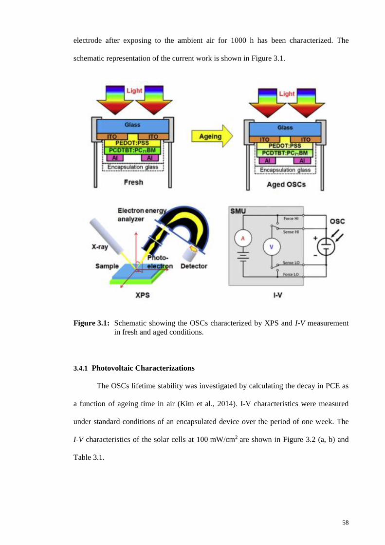
58
electrode after exposing to the ambient air for 1000 h has been characterized. The
schematic representation of the current work is shown in Figure 3.1.
Figure 3.1: Schematic showing the OSCs characterized by XPS and I-V measurement
in fresh and aged conditions.
3.4.1 Photovoltaic Characterizations
The OSCs lifetime stability was investigated by calculating the decay in PCE as
a function of ageing time in air (Kim et al., 2014). I-V characteristics were measured
under standard conditions of an encapsulated device over the period of one week. The
I-V characteristics of the solar cells at 100 mW/cm2 are shown in Figure 3.2 (a, b) and
Table 3.1.

59
Figure 3.2: The curves show (a) output power (P) vs. voltage (V), (b) I V characteristic
for fresh device, the variation in (c) Jsc, Voc, FF and (d) PCE (%)
normalized to their initial values for seven days.
From the comparison between the initial and final measurements, it can be
observed that a considerable decrease in the solar cell performance occurred due to
ageing in air. The cells initially demonstrated a reasonable PCE of 5.17% with a (Voc)
of 0.84 V, (Jsc) of 10.2 mA/cm-2 and (FF) of 60.3%. The PCE reduced to 3.61% with
Voc as 0.79 V, Jsc as 9.2 mA/cm-2 and FF as 49.8% over a period of one week. All the
photovoltaic parameters for an entire week are presented in the Table 3.1. From the
normalised parameters presented in Figure 3.2(c, d), the PCE of the solar cells rapidly
reduced initially to 70% of its initial value within first three days of ageing. The devices
observed to be relatively stable during the remaining period of time. There were no

60
significant decay recorded in (Voc) values while (Jsc) and (FF) reduced to about 87%
and 80% of their initial values respectively.
Table 3.1: Photovoltaic performance parameters for the solar cell devices calculated
prior to the device degradation tests and subsequent 7 days. Devices were
measured by global (AM 1.5 G) solar simulator.
Ageing time
(Days)
Jsc
(mA/cm-2)
Voc
(V)
FF
(%)
PCE
(%)
1 10.2 0.84 60.3 5.16
2 9.08 0.81 52.8 3.87
3 9.07 0.80 49.2 3.56
4 8.67 0.79 48.0 3.30
5 9.07 0.79 49.2 3.61
6 8.77 0.79 46.8 3.26
7 9.08 0.79 49.8 3.61
For an OSC device, the degradation phenomenon rely on both bulk and interface
phenomena, and involves degradation of the interfaces, degradation of active layer,
interfacial layers and electrode degradation, morphological, optical and macroscopic
changes such as formation of particles, bubbles, diffusion of water from atmosphere,
corrosion and diffusion of ITO, delamination and initiation of cracks and voids etc.
(Norrman et al., 2010). All these factors make this process a complex set of phenomena
and it is thus a challenging job to identify some or all of them. It becomes even more
difficult to quantify each of these degradation factors to what extent each of them
contributes in the overall deterioration of the OSCs. In this work, a more detailed
understanding of these degradation factors which cause the instability in the device
photovoltaic performance have been sought and investigated every layer of the normal
architecture cell structure. Although, the device stability data for up to 7 days (140

61
hours) of fabrication has been presented in Figure 3.2 and Table 3.1, the degradation
study was prolonged to 1000 hours in order to develop a deeper understanding of
degradation factors affecting the device performance at every layer level.
3.4.2 XPS Analysis of HTL and Photoactive Layer with Aging
To explore the effect of ambient atmosphere exposure on the chemical changes
in PCDTBT:PC71BM active layer and PEDOT:PSS HTL, XPS measurements on
PCDTBT:PC71BM and PEDOT:PSS thin films are carried out. Figure 3.3 shows the
representative survey spectra for both layers ranging from 0 to 800 eV. Data were
recorded before and after ageing of samples.
Figure 3.3: Survey spectra for (a, b) PCDTBT:PC71BM and (c, d) PEDOT:PSS films
recorded for fresh sample and after 1000 h of aging in ambient
atmosphere.

62
3.4.2.1 Change in Elemental Concentration of HTL with Ageing
Figure 3.4(a) shows the elemental concentration of PEDOT:PSS films for
freshly prepared, 250 and 1000 h ageing, whereas the data are obtained for Figure 3.4
from XPS survey spectra of PEDOT:PSS presented in the Figure 3.3. Around 1.1%
concentration of indium in freshly prepared PEDOT:PSS films was detected, whereas,
the tin concentration was almost negligible (<0.1%) until 250 h of ageing. Indium and
tin concentration reached to 17.9 and 2.1 % in 1000 h of ageing, respectively. There was
no significant increase recorded in oxygen content in first 250 h which on further
ageing of the device for 1000 h in air reached from 23.3 (freshly prepared) to 35.7 %.
Sulphur content was also reduced from 7.2% in the fresh sample to 0.7% in 1000 h aged
sample. Like oxygen, there was no significant change detected in sulphur content in first
250 h. According to Kettle et, al. in their study on chemical changes of active layer,
substantial decrease in the sulphur concentration between 250 and 1000 h is equated
with an increase in oxygen content in the similar time span (Kettle et al., 2015).
Relatively stable concentration of oxygen in first 250 h is attributed to the fact that
PEDOT:PSS initially have the tendency to both gain and loose oxygen; and initially,
until 250 h , oxygen loss offsets the oxygen gain and later oxygen gain observed to be
the dominant process (Norrman et al., 2010).
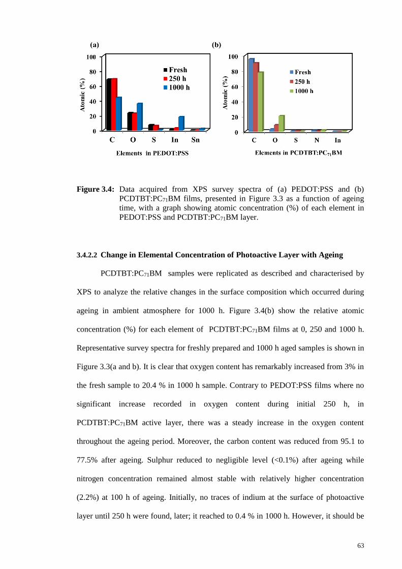
63
Figure 3.4: Data acquired from XPS survey spectra of (a) PEDOT:PSS and (b)
PCDTBT:PC71BM films, presented in Figure 3.3 as a function of ageing
time, with a graph showing atomic concentration (%) of each element in
PEDOT:PSS and PCDTBT:PC71BM layer.
3.4.2.2 Change in Elemental Concentration of Photoactive Layer with Ageing
PCDTBT:PC71BM samples were replicated as described and characterised by
XPS to analyze the relative changes in the surface composition which occurred during
ageing in ambient atmosphere for 1000 h. Figure 3.4(b) show the relative atomic
concentration (%) for each element of PCDTBT:PC71BM films at 0, 250 and 1000 h.
Representative survey spectra for freshly prepared and 1000 h aged samples is shown in
Figure 3.3(a and b). It is clear that oxygen content has remarkably increased from 3% in
the fresh sample to 20.4 % in 1000 h sample. Contrary to PEDOT:PSS films where no
significant increase recorded in oxygen content during initial 250 h, in
PCDTBT:PC71BM active layer, there was a steady increase in the oxygen content
throughout the ageing period. Moreover, the carbon content was reduced from 95.1 to
77.5% after ageing. Sulphur reduced to negligible level (<0.1%) after ageing while
nitrogen concentration remained almost stable with relatively higher concentration
(2.2%) at 100 h of ageing. Initially, no traces of indium at the surface of photoactive
layer until 250 h were found, later; it reached to 0.4 % in 1000 h. However, it should be

64
noticed that XPS with the probe depth of 5 to 10 nm does not represent the bulk
properties and represents only the surface composition. Therefore, it might be possible
that indium had already diffused from ITO surface into the PEDOT:PSS and further into
the photoactive layer but reached to the surface after 1000 h.
3.4.2.3 PCDTBT:PC71BM Chemical Changes
To ascertain the chemical changes occurred in the PCDTBT:PC71BM films due
to oxygen and indium diffusion, high resolution spectra for each element were recorded.
XPS C 1s and O 1s core-level spectra of PCDTBT:PC71BM films show new features
and broadening of both spectra after ageing as shown in Figure 3.5. The peaks in the C
1s spectra after ageing show an insignificant shift towards higher binding energies. In C
1s spectra for fresh and aged samples the components at 284.47 and 284.57 eV
respectively, are ascribed to C-C bond and the peak shape represents typical of partially-
ordered graphite-like materials (Kettle et al., 2015) (Ganguly et al., 2011; Mattevi et al.,
2009). The high energy values at 286.76 and 286.84 eV of fresh and aged samples
respectively, best match with the carbon singly or doubly bonded to oxygen i.e. O-C=O
or C-O-C bond (epoxide group) (Bhushan, 2012; Daems et al., 2014; Kumar, et al.,
2013). Whereas, the peak present in the fresh sample at 289.49 eV is corresponding to
COO- bond (carboxyl groups) as shown in Figure 3.5(a) (Jeong et al., 2008; Mattevi et
al., 2009). The intensity of the peaks had significantly reduced after ageing as shown in
the C 1s spectra in Figure 3.5(b) which is also evident in the survey spectra and
indicates the reduction in carbon content in the polymer matrix. The peak broadening in
the aged spectra indicates the significant increase of oxygenated carbon present in the
polymer, suggesting that C-O and C=O oxidation of the carbon atoms in the fullerene
might occur which cannot be distinguished due to the broadening of peaks (Kettle et al.,
2015). These oxidized species might cause severe degradation issues and OSCs
performance could significantly decrease.

65
The deconvulated O 1s spectra before and after ageing are shown in Figure 3.5.
The components at 531.37 and 531.96 eV of the fresh and aged sample ascribe to
oxygen atoms bonded with carbon atoms in functions such as ketone (C-O-C) and
carboxylic acid (COOH and/or -OC-O-CO) (Yusoff et al., 2014). The peak at 533.30
eV in the fresh sample is attributed to the C-O bond which implies that oxygen atoms
are directly bonded to carbon atoms in the polymer backbone (Mittal, 2004; Rosenthal
et al., 2010; Schweiger et al., 2015), in sound agreement with the literature values
(Kettle et al., 2015). Generally, the O species having binding energies between 531-533
eV are likely attributed to C-O or C=O species (Guo et al., 2013). In the aged sample,
the peak at 533.30 eV disappeared and a new peak at 529 eV emerged which
corresponds to C=O bond (Sabu et al.,2012).
The N 1s spectra for fresh and aged sample in Figure 3.5 showed a sharp and
defined peak at ~ 402 eV which correspond to N-O formation (Kettle et al., 2015). This
indicates the oxidation of nitrogen present in the polymer matrix. Another shoulder peak
at 402.31eV in fresh sample may also correspond to N-O surface species or an N atom
bonded to another N atom (Fuge et al., 2003; Miller et al., 2002). A new peak emerged
at 398.29 eV after ageing of sample is attributed to C-N or C=N bond (Dementjev et al.,
2000; Guo et al., 2013). The shakeup structures in both fresh and aged samples are
emerging at 404.51 and 405.31eV respectively and correspond to some form of
oxidized nitrogen species (Fechler et al., 2013; Feng, 2015; Gao, 2015; Radovic, 2004).
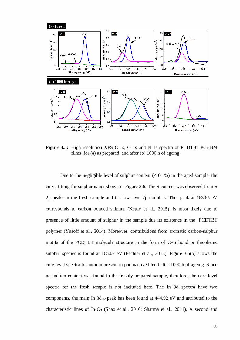
66
Figure 3.5: High resolution XPS C 1s, O 1s and N 1s spectra of PCDTBT:PC71BM
films for (a) as prepared and after (b) 1000 h of ageing.
Due to the negligible level of sulphur content (< 0.1%) in the aged sample, the
curve fitting for sulphur is not shown in Figure 3.6. The S content was observed from S
2p peaks in the fresh sample and it shows two 2p doublets. The peak at 163.65 eV
corresponds to carbon bonded sulphur (Kettle et al., 2015), is most likely due to
presence of little amount of sulphur in the sample due its existence in the PCDTBT
polymer (Yusoff et al., 2014). Moreover, contributions from aromatic carbon-sulphur
motifs of the PCDTBT molecule structure in the form of C=S bond or thiophenic
sulphur species is found at 165.02 eV (Fechler et al., 2013). Figure 3.6(b) shows the
core level spectra for indium present in photoactive blend after 1000 h of ageing. Since
no indium content was found in the freshly prepared sample, therefore, the core-level
spectra for the fresh sample is not included here. The In 3d spectra have two
components, the main In 3d5/2 peak has been found at 444.92 eV and attributed to the
characteristic lines of In2O3 (Shao et al., 2016; Sharma et al., 2011). A second and
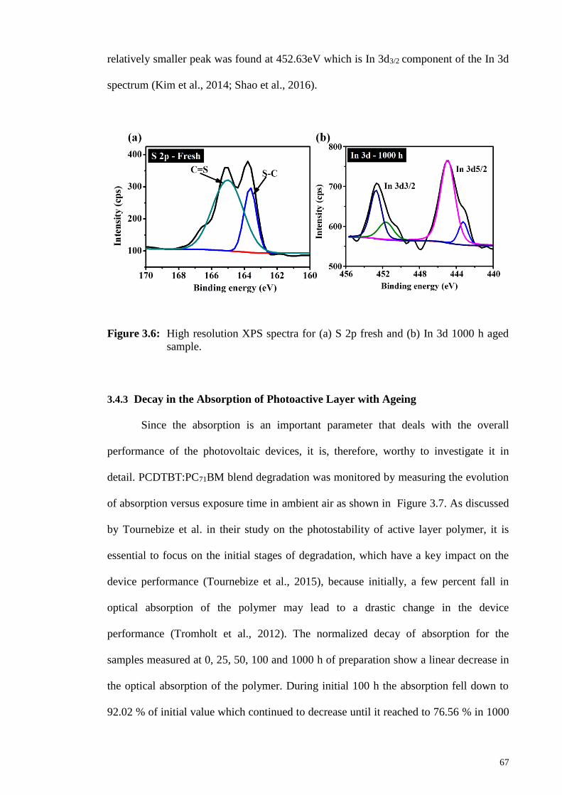
67
relatively smaller peak was found at 452.63eV which is In 3d3/2 component of the In 3d
spectrum (Kim et al., 2014; Shao et al., 2016).
Figure 3.6: High resolution XPS spectra for (a) S 2p fresh and (b) In 3d 1000 h aged
sample.
3.4.3 Decay in the Absorption of Photoactive Layer with Ageing
Since the absorption is an important parameter that deals with the overall
performance of the photovoltaic devices, it is, therefore, worthy to investigate it in
detail. PCDTBT:PC71BM blend degradation was monitored by measuring the evolution
of absorption versus exposure time in ambient air as shown in Figure 3.7. As discussed
by Tournebize et al. in their study on the photostability of active layer polymer, it is
essential to focus on the initial stages of degradation, which have a key impact on the
device performance (Tournebize et al., 2015), because initially, a few percent fall in
optical absorption of the polymer may lead to a drastic change in the device
performance (Tromholt et al., 2012). The normalized decay of absorption for the
samples measured at 0, 25, 50, 100 and 1000 h of preparation show a linear decrease in
the optical absorption of the polymer. During initial 100 h the absorption fell down to
92.02 % of initial value which continued to decrease until it reached to 76.56 % in 1000

68
h. The peaks at 377 and 479 nm exhibit slightly more pronounced decrease in the
absorption (undesired) of the aged samples which is indicative of the atmospheric
induced degradation of the polymer due its exposure to air (Endale et al., 2014).
Figure 3.7: (a) Evolution of the PCDTBT:PC71BM absorption (300-800 nm) versus
exposure time to ambient air (Fresh - 1000 h), (b) Decay of the
normalized PCDTBT:PC71BM absorption upon exposure in ambient
atmosphere.
3.4.4 Morphological Analysis of Photo-active Layer
It is evident from the photovoltaic results that a sharp decrease in the device
performance occurred within the first 72 h of device ageing, in this context; apart from
other factors the morphology of the photo-active blend layer has a crucial influence on
the device performance. Thus, AFM and SEM analysis of PCDTBT:PC71BM photo-
active layer were performed for freshly prepared and 72 h aged samples. AFM images
in Figure 3.8 show the evolution of surface morphology with aging, both freshly
prepared (Figure 3.8b) and 72 h (Figure 3.8d) aged samples revealed quite smooth
surface with almost similar morphological features, however, the root mean square
roughness (RMS) value, in an area of 1 µm × 1 µm, for the aged films (1.86 nm) is
much greater than that of freshly prepared (1.07 nm) sample. The SEM images also
present a flat sheet of polymer with morphology features very similar to that observed

69
in AFM images. Some impurities or probably some clusters of the organic material
were found on the surface (i.e. encircled in the Figure 3.8c) of 72 h aged sample which
likely occurred due to aggregation of organic constituents of photo-active layer with the
ageing, in good agreement with previously reported data (Seck et al., 2015).
3.4.5 SEM Analysis of Aluminium Electrode Degradation
Effect of Al cathode exposure to the high humidity air has also been
characterized. The devices were exposed to ambient air in order to observe the possible
damage due to water ingress. SEM results exhibit severe damage of Al electrodes
caused by moisture and oxygen. SEM images of the freshly deposited Al electrode in
Figure 3.9 (a, b) exhibit a void-free surface without much height deviation. Moreover,
SEM images in both fresh and aged sample show grain surface texture consisting of
small Al grains. Although the grains are densely packed, however, no definite order
(a
)
(c
)(d
)
(b
)
Figure 3.8: SEM and AFM images of PCDTBT:PC71BM films (a, b) Fresh and (c, d)
after 72 h of ageing at ambient atmospheric conditions.

70
among them is visible, in good agreement with previously reported results (Kaune et al.,
2011). Whereas, in the aged samples (Figure 3.9 (c, d)) micron sized voids and bubble-
like protrusions appeared which are similar to the previously reported ageing effects
(Glen et al., 2015).
Figure 3.9: FESEM images of Al electrodes for (a, b) as deposited samples and (c, d)
after exposing to the ambient atmosphere for 1000 h.
3.5 Discussion
From the XPS and photovoltaic results, it is believed that the OSCs in ambient
air exhibit significant instability due to indium and oxygen diffusion into the HTL as
well as the photoactive layer. The devices and films were tested under prolonged
exposure to ambient air. It is evident from the photovoltaic results that the device
initially showed rapid decay in efficiency, however, relatively stable performance of the

71
device after 72 h and until 1000 h is attributed to the proper encapsulation of the devices
which overcomes the device degradation and limits the hazardous effect of ambient air
on the device performance but it is expected to die within very short time of fabrication
in case of an un-encapsulated device (Stratakis et al., 2014). The sharp decay in the
device photovoltaic performance within 24 hours is mainly attributed to the instability
of the interface between ITO and PEDOT:PSS. Initially the degradation is
predominately due to indium diffusion which immediately started after spin coating of
PEDOT:PSS HTL and 1.1% concentration of indium on the surface of freshly prepared
PEDOT:PSS films has been detected. PEDOT:PSS etches indium out of ITO which
leads to the incorporation of indium in the photoactive layer. The diffusion of indium
into the active layer could result in quenching of excitons and accelerates the charge
recombination rate due to its ability to act as the charge trapping center (Chen et al.,
2013; Warren et al., 1992). This would result in the decay of Jsc and FF of the device
and, therefore, decrease the lifetime stability of the device. Moreover, as the time
passes, the efficiencies keep on deteriorating, where after just three days of fabrication
the PCE of the device plunges to around 70 % from its initial efficiency, shown in
Figure 3.2(d). The decay in the efficiency is mainly attributed to the significant (about
20%) decrease in the FF and around 10% decrease in the Jsc, however, the Voc of the
OSCs remained almost stable with only 5% reduction in its initial value as shown in
Figure 3.2(c). In addition, formation of In2O3 and presence of oxygenated species
caused by oxygen diffusion have been observed to restrict the overall device
performance. Interestingly, during the XPS analysis of exposed films of HTL, it was
observed that initially the dominating degradation factor is the diffusion of indium
which started immediately after the spin coating of PEDOT:PSS HTL. Chang & Chen
in their recent investigation on the PEDOT:PSS and ITO interaction, showed that
dissolution of indium in PEDOT:PSS aqueous solution also decrease the work function

72
(Chang & Chen, 2007). This would lead a device to degradation even after
encapsulation, predominately in the FF and Jsc as observed in our work. In case of
longer hours of exposure to air, oxygen is also in play along with indium diffusion into
the HTL which would also accelerate the indium diffusion (Kawano et al., 2006).
Contrary to HTL, degradation process in PCDTBT:PC71BM photoactive layer
was predominately due to oxygen diffusion (Figure 3. 4) which continuously increased
in 1000 h. Oxygen can be absorbed from the atmosphere into the active layer through
the Al electrodes. Al easily gets oxidize which cause voids and pinholes in case of
longer exposure to moisture. These voids facilitate the diffusion of moisture into the
underneath layers (Kawano et al., 2006; Seeland et al., 2011) , and this whole oxidation
process consequently increases the series resistance (Rs). In addition, areas which are
affected by these voids due to deterioration of Al are unlikely to have any contribution
towards a working device. Since the photo-active layer and Al electrode will lose
contacts in the region under voids, therefore, any free charge carriers generated in this
region will be likely to recombine rather than being extracted by the electrode. Hence,
Al-active layer interface will act as a charge blocking layer and grow as a function of
exposure time to air. This phenomenon significantly accounts in total efficiency loss
with time (Glen et al., 2015).
Although, there was no significant change recorded in the morphology of fresh
and 72 h aged samples except for the increase in the surface roughness, however, it is
vital to record the initial changes in the morphology of the blend film due to ageing
because a small deterioration of the morphology could have a drastic effect on the
device performance (Tournebize et al., 2015; Tromholt et al., 2012). However, in this
work, it is believed that root cause of device degradation is the diffusion of indium into
the photoactive layer and the increase in the surface roughness is likely to add in the
73
overall device degradation as smooth and homogeneous surface is highly desired for an
optimum device performance.
The decay in the optical properties of the active layer blend is likely ascribed to
deterioration of polymer morphology due to its reaction with ambient atmosphere or
even with PEDOT:PSS (Tournebize et al., 2015). Our results match well with observed
decay in device photovoltaic stability (Figure 3.2); in addition, XPS survey spectra also
confirm the oxygen/moisture ingress into the polymer blend and later on indium
diffusion from ITO surface to the photo active layer which could likely hinder its
absorption.
The study presented here demonstrate that ageing in ambient air leads to an
overall performance loss of PCDTBT:PC71BM based OSCs. Basically, all the
characterizations techniques revealed decay in the morphological, compositional and
electrical parameters of an OSC with time. Finally, it is vital to note that the presented
fabrication procedure is a facile route to ensure a low cost device, since it can be
processed on light-weight and flexible substrates, and therefore compatible with large
scale roll to roll production. The device performance can be improved by ensuring
extrinsic and intrinsic stability with proper encapsulation and finding the alternative of
PEDOT:PSS which should not corrode the ITO surface.
3.6 Conclusions
In summary, the degradation process mainly based on chemical and optical
changes related to materials and interfaces in BHJ OSCs, has been studied. The XPS
data show chemical changes that occur in PCDTBT:PC71BM photoactive layer under
ambient atmosphere. The photoactive blend appears as an oxygen containing polymer
with oxidation of carbon and nitrogen atoms. XPS survey spectra confirm the
penetration of indium and tin into the PEDOT:PSS HTL and further into the photoactive

74
layer. Substantial increase in indium content at HTL surface in initial 250 h of ageing
shows that degradation in HTL initially was predominantly due to indium diffusion
which upon ageing for 1000 h also affected by remarkable increase in oxygen content.
Whereas, a steady increase in oxygen content at the surface of photoactive layer, has
been observed. It was concluded that photoactive material and its interface with HTL
and cathode is strongly affected by moisture diffusion along with the diffusion of
indium from ITO surface. Optical properties of the device were also affected in ambient
atmosphere and the low absorption after degradation was observed. The power
conversion efficiency was reduced due to decrease in Jsc and FF. Overall, this study
show the degradation effects related to oxygen and indium diffusion in the photoactive
layer and its interface with PEDOT:PSS and Al cathode. It is suggested that higher
performance of the device could be achieved by adopting intrinsic and extrinsic stability
measures.

75
STABILITY ENHANCMENT IN ORGANIC SOLAR CELLS BY
INCORPORATING V2O5 NANOPARTICLES IN THE HOLE
TRANSPORT LAYER3
4.1 Overview
Synthesis The synthesis of V2O5 nanoparticles by a hydrothermal method and
their utilization in a PEDOT:PSS buffer layer in a PCDTBT:PC71BM device structure is
demonstrated. V2O5 nanoparticles were dispersed in the PEDOT:PSS HTL in normal
architecture BHJ solar cells. The device performance for both pure PEDOT:PSS and
hybrid HTLs were studied and demonstrated to effectively work in BHJ OSCs. From
the stability test initially for one week and subsequently for another three weeks, it was
confirmed that the OSC device with the incorporation of V2O5 nanoparticles in the
standard HTL leads to a decrease in device degradation and significantly improves the
lifetime as compared to the standard HTL based device. Moreover, the hybrid HTL
exhibits better optical properties and a relatively stable band gap as compared to its
pristine PEDOT:PSS counterpart. The results indicate that V2O5 could be a simple
addition into the PEDOT:PSS layer to overcome its stability and degradation issues
leading to an effective HTL in BHJ OSCs.
4.2 Introduction
OSCs have gained considerable attraction due to their friendliness to the
environment, cheaper generation cost, compatibility with green energy systems and
large scale roll to roll production (Huang et al., 2012; Sun et al., 2010). BHJ-OSCs are
3 The work presented in Chapter 4 has been published in RSC: “RSC Advances (Rank: Q1, Impact Factor: 3.29)” as
Rafique et al. (2016). Stability enhancement in organic solar cells by incorporating V2O5 nanoparticles in the hole transport layer.
RSC Advances, 6(55), 50043-50052.

76
based on an intimate blend of a donor and an acceptor material within the active layer
matrix which is then phase separated while coating to create a donor acceptor interface
(Irwin et al., 2011; Kettle et al., 2012; Li et al., 2010). Photons are absorbed by these
materials to generate excitons which diffuse to the donor–acceptor interface and
dissociate into the charge carriers. These charge carriers are then extracted by the
respective electrodes (Scharber & Sariciftci, 2013; Wright & Uddin, 2012). These solar
cells have layered geometric structure and optimization of each layer is essential to
achieve overall performance of the device. It is very important in BHJ OSCs to achieve
good ohmic contacts and charge transportation between the electrodes and the active
layer. This is limited by the deep energy levels of the donor polymers which create a
barrier at the interface between the active layer and either of the electrodes (Griffin,
2014). In order to overcome these issues, HTL and ETL are introduced at the interface
between active layer and the electrodes (Duan et al., 2013; Irwin et al., 2011; Jørgensen
et al., 2012).
PEDOT:PSS is considered as one of the most widely used HTL materials for the
efficient charge transportation. However, there are several stability issues associated
with this material due to its shallower energy levels and acidic nature which turns the
device to degrade rapidly (Hancox et al., 2012; Schulz et al., 2014; Steirer et al., 2010).
In recent years, a lot of research has been carried out to overcome the shortcomings of
PEDOT:PSS. Metal oxides have been proved to be a good alternative to it (Lattante,
2014). These metal oxides serve many functions in an OSC such as their use as an
active material, transparent electrodes, charge blocking and extraction layers, optical
spacers and at the same time they are helpful in enhancing the stability and efficiency
(Gershon, 2011). There are several transition metal oxides such as V2O5, NiO, Cs2CO3,
WO3 and MoO3 which are being used in the BHJ solar cells and exhibit a wide range of
energy levels. Many of them are proved to be more stable than PEDOT:PSS due to their

77
intrinsic optical, structural and electrical properties (Irani et al., 2013; Julien et al., 2012;
Mane et al., 2015; Meyer et al., 2011; Ryu & Jang, 2011; Shrotriya et al., 2006;
Zilberberg et al., 2011). In general, metal-oxide charge extraction layers demonstrated
to be a good addition in OSCs with overall improvement in efficiency and stability (Ryu
& Jang, 2011; Shrotriya et al., 2006).
V2O5 is one of the most widely explored materials as an n-type semiconductor
due to its very good transparency, wide optical ban dap, and good stability (Irani et al.,
2013; Mane et al., 2015). In addition, this metal oxide also provide good interfacial
adhesion and enhances the device stability significantly when exposed to ambient
environment which are limiting factors in case of PEDOT:PSS HTL (Meyer et al.,
2011; Zilberberg et al., 2011). There are several methods which have been employed in
the past to deposit this material as an HTL in BHJ OSCs both in normal as well as in
inverted structures. Vacuum deposited processes had been widely used to deposit V2O5
in the past but these processes are not compatible with the large scale production on
account of their high manufacturing costs which lead to a substantial addition in the
overall fabrication cost of the device (Julien et al., 2012; Liu et al., 2014). In recent
years, efforts have been made to solution deposit the V2O5 by using different techniques
such as brush painting (Cho et al., 2015), solution processed spin coating (Hancox et al.,
2012), sol–gel derived vanadium oxide (Kololuoma et al., 2015; Zilberberg et al.,
2011), and several other methods (Irani et al., 2013; Julien et al., 2012; Mane et al.,
2015; Meyer et al., 2011; Ryu & Jang, 2011; Shrotriya et al., 2006; Zilberberg et al.,
2011). However, still a lot of work is needed to be done to find the best and cheaper
ways to deposit these oxides, for optimizing the material properties to get the highly
efficient devices compatible with PEDOT:PSS and exhibiting high stability.
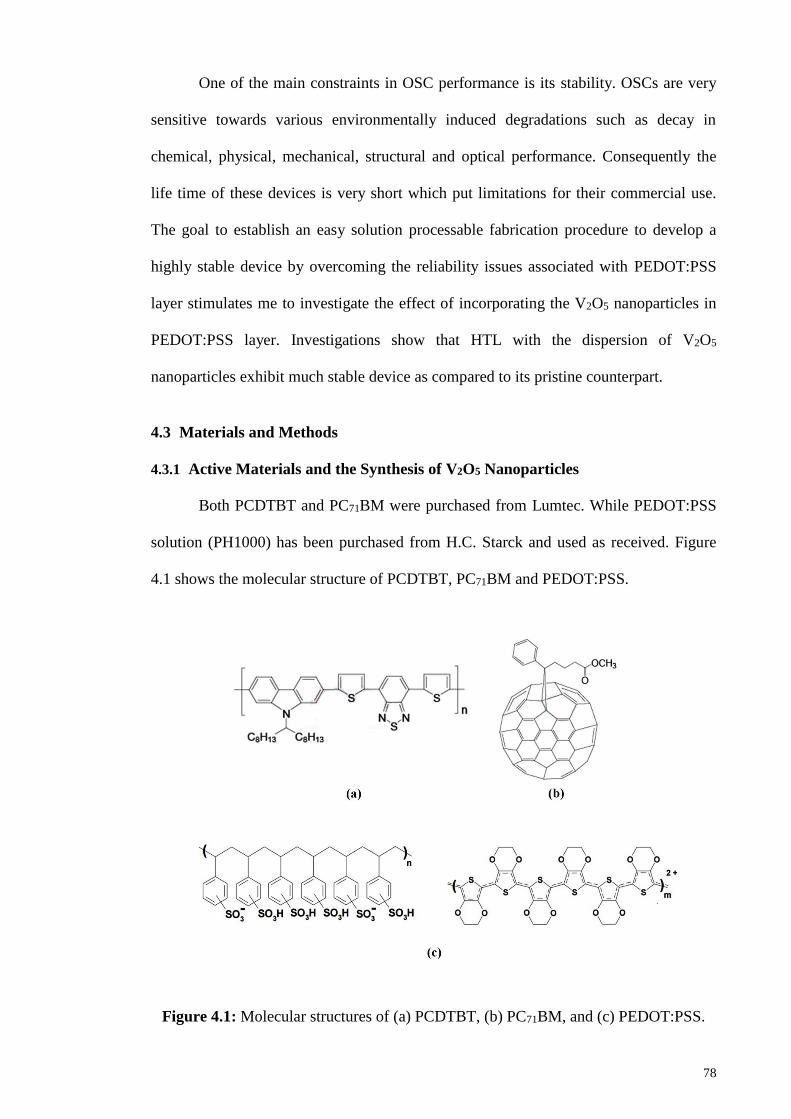
78
One of the main constraints in OSC performance is its stability. OSCs are very
sensitive towards various environmentally induced degradations such as decay in
chemical, physical, mechanical, structural and optical performance. Consequently the
life time of these devices is very short which put limitations for their commercial use.
The goal to establish an easy solution processable fabrication procedure to develop a
highly stable device by overcoming the reliability issues associated with PEDOT:PSS
layer stimulates me to investigate the effect of incorporating the V2O5 nanoparticles in
PEDOT:PSS layer. Investigations show that HTL with the dispersion of V2O5
nanoparticles exhibit much stable device as compared to its pristine counterpart.
4.3 Materials and Methods
4.3.1 Active Materials and the Synthesis of V2O5 Nanoparticles
Both PCDTBT and PC71BM were purchased from Lumtec. While PEDOT:PSS
solution (PH1000) has been purchased from H.C. Starck and used as received. Figure
4.1 shows the molecular structure of PCDTBT, PC71BM and PEDOT:PSS.
Figure 4.1: Molecular structures of (a) PCDTBT, (b) PC71BM, and (c) PEDOT:PSS.

79
V2O5 nanoparticles were synthesis by hydrothermal method. 1 mM of vanadium
acetylacetonate was dissolved into 40 mL of deionized water. 10 mg of Hexa-decyl-
trimethyl ammonium bromide (CTAB) and 5 mg of trimethylamine N-oxide were
dissolved into 20 mL of deionized water. This solution was added drop by drop into the
vanadium solution under stirring at 80 °C and left at this temperature for 30 minutes.
Whole mixture was transferred to Teflon-lined stainless steel autoclave with capacity of
80 mL and put into an electric oven at 150 °C for 2 hours. The product was collected by
centrifuge at 5000 rpm for 1 min, then washed several times with deionized water and
left to dry at 50 °C in the oven under vacuum overnight. The powder was followed by
calcinations at 450 °C for 2 hours to finally obtain yellowish-brown V2O5 nanoparticles.
The flow chart for the synthesis procedure has been presented in Figure 4.2.
Figure 4.2: Flow chart of V2O5 nanoparticles synthesis via hydrothermal method.
80
4.3.2 Solar Cell Fabrication Procedure
Pre-patterned ITO coated glass substrates, for device fabrication, were provided
by Ossila Ltd. UK. The dimensions of the rectangular substrates were 1.5×2.0 cm, with
six active pixels on each substrate and an active area of 3×1.5 mm (4.5 mm2) for every
pixel. Those were cleaned first by using normal soap and then sequential ultrasonication
in deionized water, acetone and isopropanol for 15 min each. At the end, substrates
were dried by (Nitrogen) N2 stream and treated by O2 plasma for 5 minutes.
PEDOT:PSS was spun coated at 4000 rpm for 1 min and then dried at 120 °C for 30
minutes to achieve the final layer thickness of around 40 nm. The active layer is
consisting of PCDTBT as donor material and PC71BM as an acceptor material. The
active layer ingredients were dissolved in chloroform with a concentration of 10 mg
mL-1 and then mixed with the volume ratio of 1: 4 (PCDTBT:PC71BM). Mixing was
performed by stirring them for 24 hours. After transferring samples into nitrogen-filled
glove-box, the final blended active layer was spun coated at 2000 rpm for 20 seconds.
Al electrode with thickness of 100 nm was deposited on top of the active layer in
vacuum (<10-6 torr) by means of thermal evaporation. Finally, all the OSCs devices
were encapsulated by sticking a thin glass slide to cover active area of the device using
a drop of epoxy glue. In the second set of experiments, PEDOT:PSS was mixed with the
V2O5 nanoparticles at the concentration of 1 mg mL-1 and coating parameters were
optimized for the desired thickness of 40 nm. Same fabrication procedure was adopted
which is described previously. Figure 4.3 shows two types of fabricated OSCs varied by
their HTLs including the energy band diagram for both of them.

81
Figure 4.3: Device structure of PCDTBT:PC71BM solar cells with (a) PEDOT:PSS,
(b) PEDOT:PSS + V2O5 as HTL, and the energy diagram for solar cells
with (c)PEDOT:PSS, and (d) PEDOT:PSS + V2O5 as HTL.
4.3.3 Characterization
4.3.3.1 Characterization of V2O5 Nanoparticles
V2O5 nanoparticles were first characterized for their compositional and structural
properties. XRD was performed in 2θ scanning range of 10 to 60° by using Ultima-IV
(Rigaku, Japan) multipurpose X-ray diffraction system. Powder diffractometer,
equipped with Cu K-a source (λ=0.154060 nm) was used to obtain the X-ray diffraction

82
pattern. Energy dispersive X-ray analysis along with FESEM was performed to obtain
the elemental composition by using EDS OXFORD INCA ENERGY 250 (Oxford
Instruments, UK) attachment. Raman spectroscopy was performed to measure Raman
shifts by a DXR Raman Microscope (Thermo Scientific, USA), equipped with green
light excitation (532 nm) laser source at 6 mW power.
4.3.3.2 Characterization of OSC Devices
Thickness of the HTL consisting of a mix blend of PEDOT:PSS and V2O5 was
measured by surface Profiler (DEKTAK 150 Veeco, UK). Morphological
characterizations were carried out by FESEM model JEOL JSM-7600F, Japan and
AFM model SPM PROBE VT AFM XA 50/500 Omicron, Germany. Optical
measurements of the samples were carried out with the UV-vis spectrophotometer
(Perkin Elmer Lambda 750, USA). I-V characteristics of the solar cells were measured
by Keithley 236 Source Measure Unit. Solar cell performance was tested by using an air
mass 1.5 Global (AM 1.5 G) solar simulator with an irradiation intensity of 100 mW
cm-2. The light intensity calibration was performed with a Newport power meter 1918-R
with calibrated Si-detector 818-UV.
4.4 Results and Discussion
4.4.1 Structural and Morphological Analysis
XRD pattern of the prepared V2O5 nanoparticles is presented in Figure 4.4(a).
All the peaks are well indexed to the ICDD PDF-2 (Release 2011) DB card number 01-
077-2418 and represent the intense reflections at 15.4126, 20.3651, 21.7817,
26.1387,v31.0528, 32.4078, 33.3502, 34.3418, and 41.3024° . 2θ diffracted peaks show
sharp and noise free spectra which confirm the high Crystallinity and well-arranged
orthorhombic symmetry of V2O5 crystal structure (space group: Pmmn (59)) with cell
83
dimensions as a = 11.5120, b = 3.5640, c = 4.3680. Both XRD and EDS (Figure 4c)
results confirm the high purity of the prepared material.
Phase purity of the synthesized V2O5 nanoparticles was confirmed by the Raman
spectroscopy due to its high sensitivity towards crystalline V2O5 nanoparticles (Wachs
& Routray, 2012). Determined spectrum matched well with the reported spectra (Aslam
et al., 2015; Lee et al., 2003) and shown in the inset of Figure 4.4(b). The peak at
995cm-1 is assigned to the terminal oxygen (V-O) stretching mode occurring due to
unshared oxygen. Bands at 696cm-1 and 526 cm-1 are attributed to V-O-V stretching
modes. Peaks at 406cm-1 and 283cm-1 are exhibiting the bending vibrations of V = O
bonds whereas peaks at 487cm-1 and 303 cm-1 also represent the bending vibrations of
different oxygen bonds. Raman peaks at 194cm-1 and 142cm-1 represent the lattice
vibrations (Aslam et al., 2015; Lee et al., 2003).
Two variants of HTL were also characterized for Raman shifts since it is a
powerful tool to study the conducting polymers. Resulting spectra for both HTLs are
represented in the Figure 4.4(b). Attributions of peak positions are consistent with
several reported results (Chang et al., 2014; Teng et al., 2013), showing dominantly the
characteristics for PEDOT in either case and contribution of PSS is almost negligible in
both cases. Peaks observed at 1563 cm-1, 1500cm-1, 1440cm-1, 1360cm-1, 1252cm-1 and
986cm-1 are assigned to PEDOT. Moreover, the most obvious difference brought by the
addition of V2O5 nanoparticles was observed between 1252cm-1 and 1563 cm-1. These
nanoparticles reduced the intensity of the Raman fingerprints for the peaks attributed to
1252cm-1, 1360cm-1, 1440cm-1, 1500cm-1 and 1563 cm-1, furthermore they exhibited
narrower band as compared to pristine HTL (Chou et al., 2015; Sakamoto et al., 2005).
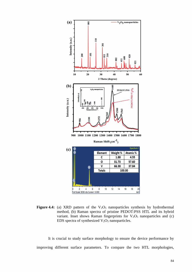
84
Figure 4.4: (a) XRD pattern of the V2O5 nanoparticles synthesis by hydrothermal
method, (b) Raman spectra of pristine PEDOT:PSS HTL and its hybrid
variant. Inset shows Raman fingerprints for V2O5 nanoparticles and (c)
EDS spectra of synthesized V2O5 nanoparticles.
It is crucial to study surface morphology to ensure the device performance by
improving different surface parameters. To compare the two HTL morphologies,

85
FESEM and AFM characterizations were used. High resolution FESEM images and
AFM morphology of both HTLs are presented in Figure 4.5.
Figure 4.5: FESEM and AFM images for (a, c) pristine PEDOT:PSS HTL and
(b, d) Hybrid HTL.
SEM image of the pristine PEDOT:PSS (Figure 4.5(a)) layer shows the smooth
and featureless surface morphology as compared to hybrid HTL. Whereas, the hybrid
HTL exhibits a loosely packed surface morphology (Figure 4.5(b)); the globules
aggregation of discrete nanoparticles on the entire surface are likely to be V2O5 particles
uniformly distributed within the polymer matrix which confirms the method efficacy of
the solution processed fabrication technique that was used to prepare HTLs. Hybrid

86
HTL shows formation of channels like morphology likely caused by nucleation effect of
V2O5 particles. Figure 4.5(c) and (d) shows the non-contact tapping mode AFM images
of pristine and hybrid HTLs deposited on ITO coated glass substrates. The morphology
of the PEDOT:PSS HTL is much smoother than hybrid HTL and surface roughness
increased to double due to addition of V2O5 nanoparticles. The increase in the
roughness was expected and agrees with the reported results in (Huang et al., 2009).
Although the roughness of the HTL had increased with the addition of V2O5
nanoparticles but it is believed that the particles dispersed on the surface of the HTL can
effectively extract the charged carrier due to their high conductivity and at the same
time they assist in reducing the leakage current by blocking the negative charge carriers
which in turns guarantees a better and stable device. It is reported that the RMS
roughness of modified HTL increases slightly with the increase of V2O5 concentration
in PEDOT:PSS except for high ratio of doping concentration (1:1) ( Kim et al., 2015).
In this work, it is observed that the addition of V2O5 in small amount (1 mg) into
PEDOT:PSS has also altered the roughness of modified HTL as shown in Figure 4.5(d).
However, the change in device performance is believed to be due to the change in
electronic and optical properties of the HTL compared to the morphological change
such as the roughness (Kim et al., 2015). Further details are presented in Section 4.4.2.
4.4.2 Optical Transmittance and Band-gap Calculations
In Figure 4.6(a), the transmittance spectra of pristine (PEDOT:PSS) HTL and
hybrid HTL (PEDOT:PSS + V2O5) to distinguish the ageing effect on the optical
properties of the both variants have been reported. Data are shown for the freshly
prepared and one month aged samples. The transmittance curves for hybrid HTL show
high transmittance of more than 94% in the visible region and did not show any
significant reduction in transmittance over one month ageing period. Whereas, the
transparency of the pristine PEDOT:PSS of freshly prepared sample is exhibiting

87
around 89 % transmittance which diminished to 84 % after one month of preparation.
It is notable that transmittance of the pristine PEDOT:PSS thin film reduced with time
which is undesirable (Sarker et al., 2015). Relatively higher degree of transparency in
the hybrid HTL ensures more light absorption by the active layer and therefore an
increase in the photo-generation of charges (Ecker et al., 2011).
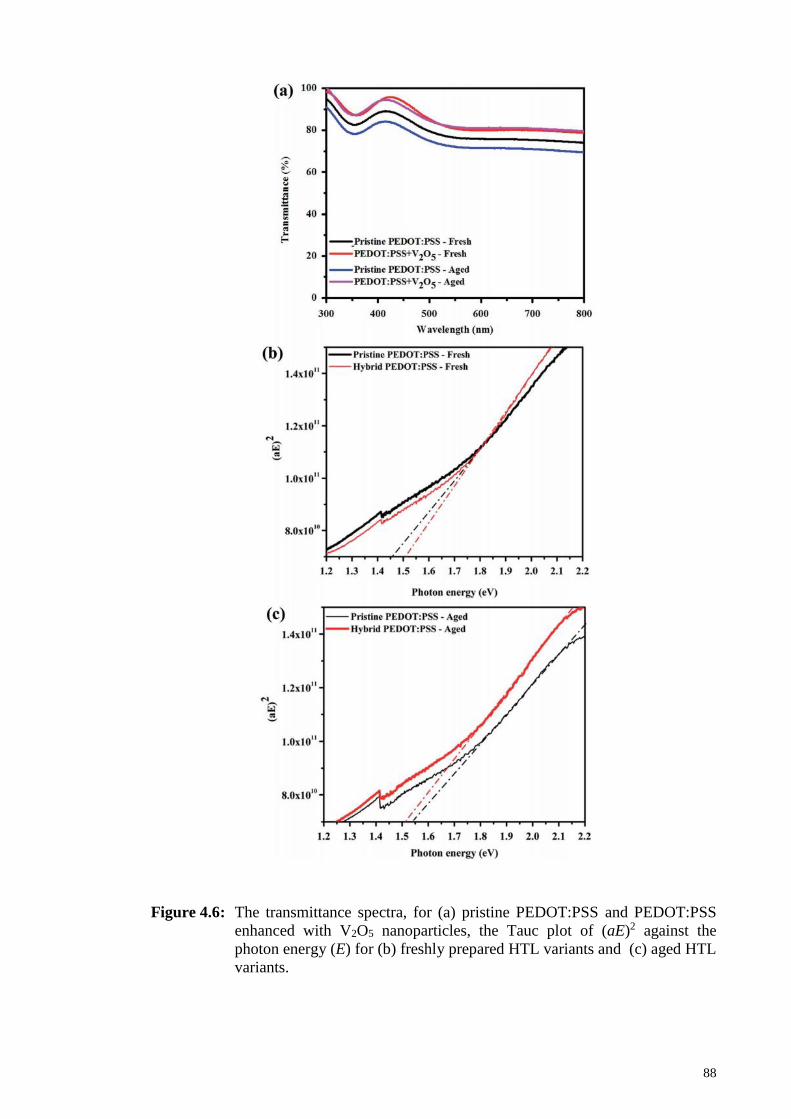
88
Figure 4.6: The transmittance spectra, for (a) pristine PEDOT:PSS and PEDOT:PSS
enhanced with V2O5 nanoparticles, the Tauc plot of (aE)2 against the
photon energy (E) for (b) freshly prepared HTL variants and (c) aged HTL
variants.

89
In Figure 4.3(c) and (d), the energy band diagram has been presented based on
their known energy levels which consist of LUMO and HOMO values. It can be seen
that the presence of V2O5 has further facilitated the extraction of holes from the active
component (PCDTBT) to PEDOT:PSS layer and then to the ITO via V2O5. In
principle, a significant difference of V2O5 LUMO level as compared to LUMO levels of
both PEDOT:PSS and the active component (PCDTBT) has potentially created a
restriction for electrons flow to the ITO and consequently made V2O5 as good electron
blocking component between the ITO/active layer interfaces. In this section, the optical
energy gaps for the freshly prepared and aged samples of pristine and hybrid
PEDOT:PSS HTLs have been determined via the optical absorption spectroscopy. The
square of absorption coefficient and photons energy (αE)2 is related to the band gap (Eg)
and calculated by the following expression (Mane et al., 2015; Reddy et al., 2013).
𝛼ℎ𝑣 = 𝛼𝑂(ℎ𝑣 − 𝐸𝑔)𝑛
…………… (4.1)
Where Eg is the band gap corresponding to a particular transition occurring in
the samples, v is the transition frequency, h is Planck's constant, n is the exponent
which can be taken as 1/2, 3/2, 2 and 3 depending on the band transition classifications.
Whereas, α = 2.303 A/t, A and t are absorption and thickness of the films respectively
(Muhammad & Sulaiman, 2011). Extrapolated values from the straight line to the
abscissa determine the optical band-gap. Figure 4.6(b) and (c) show the Tauc plot, i.e.
(aE) 2 versus photon energy of pristine and hybrid HTLs. For the direct allowed
transition, the optical band gap transition energy for pristine PEDOT:PSS varied from
1.46 to 1.55 eV when the data were collected after one month. Whereas, the optical
energy gap for hybrid HTL was found to be around 1.51 eV slightly higher than the
energy gap of fresh pristine PEDOT:PSS HTL which is believed to be due to the
presence of V2O5 nanoparticles, a well-known high work function metal oxide.

90
However, it remained unchanged during this period of time exhibiting high degree of
stability in the transition energy which consequently helps in improving the device
performance especially in cell stability. Thus, the improvement in the device
performance is also attributed to the optical properties of V2O5 (Lee et al., 2014). The
variation in transmittance and band gap energy of the both variants of HTL are
summarized in Table 4.1.
Table 4.1: The variations in transmittance and band gap energy of pristine and hybrid
HTLs due to ageing for one month.
Sample
Transmittance
(%)
Band gap energy
(eV)
Fresh Aged Fresh Aged
Pristine PEDOT:PSS 89 84 1.46 1.55
PEDOT:PSS+ V2O5 94 94 1.51 1.51
4.4.3 Organic Solar Cell Device Characteristics
Photovoltaic properties of the OSCs based on PCDTBT:PC71BM active layer
with pristine HTL, PEDOT:PSS, and its modified variant with the incorporation of
V2O5 nanoparticles were investigated. The efficiency and life time stability of both
types of devices were investigated by performing I–V measurements and reduction in
the PCEs was recorded over a period of 4 weeks. The solar simulations were performed
at the light intensity of 100 mW cm-2. Figure 4.7 shows the I–V characteristics for both
OSCs. The two variants of OSCs showed a decline in both (Jsc) and (Voc) as shown in
Figure 4.7(a) and (b). However, OSC devices with pristine PEDOT:PSS HTL exhibited
more decay in both parameters than that of with hybrid HTL. After the first week, the
pristine device demonstrated a minor degradation, mainly the decrease of the device
(Voc) from 0.8 to 0.75 V. After four weeks the device continued to degrade and (Voc)
value reduced to 0.70 V. While, in the hybrid device the (Voc) for freshly prepared

91
device is about 0.85 V which showed minor degradation in first week with (Voc) of 0.80
V. After four weeks the hybrid device showed no further reduction in the (Voc).
Figure 4.7: The current-voltage (I-V) characteristic in fresh condition, after one week,
and after 4 weeks for OSCs with (a) PEDOT:PSS, and (b)
PEDOT:PSS+V2O5 HTL layer.
From the normalized efficiency calculated over the period of four weeks as
shown in Figure 4.8, it is evident that that device with the hybrid HTL was consistently
much stable as compared to the device with pristine PEDOT:PSS layer. It retained
about 90 % of its efficiency, whereas the standard device reduced to around 65 % of its
initial efficiency over this entire period of time.
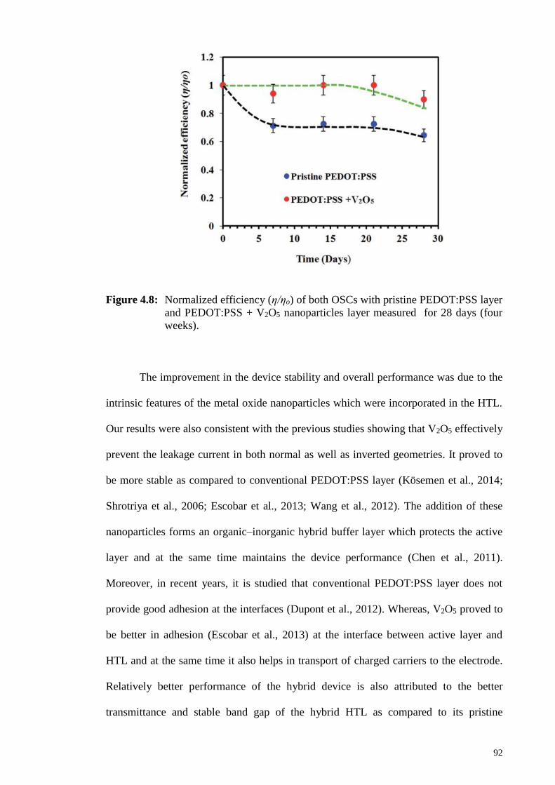
92
Figure 4.8: Normalized efficiency (η/ηo) of both OSCs with pristine PEDOT:PSS layer
and PEDOT:PSS + V2O5 nanoparticles layer measured for 28 days (four
weeks).
The improvement in the device stability and overall performance was due to the
intrinsic features of the metal oxide nanoparticles which were incorporated in the HTL.
Our results were also consistent with the previous studies showing that V2O5 effectively
prevent the leakage current in both normal as well as inverted geometries. It proved to
be more stable as compared to conventional PEDOT:PSS layer (Kösemen et al., 2014;
Shrotriya et al., 2006; Escobar et al., 2013; Wang et al., 2012). The addition of these
nanoparticles forms an organic–inorganic hybrid buffer layer which protects the active
layer and at the same time maintains the device performance (Chen et al., 2011).
Moreover, in recent years, it is studied that conventional PEDOT:PSS layer does not
provide good adhesion at the interfaces (Dupont et al., 2012). Whereas, V2O5 proved to
be better in adhesion (Escobar et al., 2013) at the interface between active layer and
HTL and at the same time it also helps in transport of charged carriers to the electrode.
Relatively better performance of the hybrid device is also attributed to the better
transmittance and stable band gap of the hybrid HTL as compared to its pristine
93
counterpart. Furthermore, it mitigated the adverse effects of PEDOT:PSS acidic nature
on ITO over the time due to its favorable optical, structural and electrical properties
which in turns had given us a more stable device as compared to the standard cell.
4.5 Conclusions
This work has successfully demonstrated the fabrication of air
stable PCDTBT:PC71BM based polymer solar cells with V2O5 modified HTL to address
the reliability issues associated with conventional PEDOT:PSS layer. The results show
that the mixing of V2O5 + PEDOT:PSS has a major impact on the device life time
stability. Based on this study, results were evident that V2O5 based HTL could
significantly reduce the degradation in OSCs device performance than pristine
PEDOT:PSS HTL. The device with hybrid HTL retained 90 % of its PCE even after
four weeks of ageing compared to the pure PEDOT:PSS HTL where overall efficiency
reduced to around 65 % of its initial value. In addition to remarkably better stability,
both HTLs and active layers were fabricated by the simple and solution processed
method, which greatly simplifies the fabrication process and reduced the overall cost.
This study thus showed the importance of buffered layers in OSCs with an emphasis on
improving the HTL if long operational devices are to be achieved. A further in depth
study of metal oxide based HTLs and their interfaces with the BHJ and ITO electrodes
are needed to be investigated in future.

94
BULK HETEROJUNCTION ORGANIC SOLAR CELLS WITH
GRAPHENE OXIDE HOLE TRANSPORT LAYER: EFFECT OF
VARIED CONCENTRATION ON PHOTOVOLTAIC
PERFORMANCE4
5.1 Overview
This chapter reports the solution processable hole transport layer (HTL) for
bulk heterojunction organic solar cells (BHJ OSCs) based on varied concentration of
graphene oxide (GO) in aqueous suspension. The effects of varied concentration of GO
at 1, 2 and 4 mg/ml on the morphological, optical, electrical and photovoltaic properties
of the OSCs have been studied. Device with the lowest concentration and least
thickness of GO showed most optimized performance with a power conversation
efficiency (PCE) of 2.73 % as compared to the higher concentration where the PCE
reduced to 0.67 and 0.22 % for the devices with HTL of 2 and 4 mg/ml, respectively.
The remarkable reduction in the device performance at higher concentration is mainly
attributed to a drastic decrease in the short circuit current that reduced from
8.14mA/cm2 to 2.90 and 1.10 mA/cm2at 2 and 4 mg/ml, respectively. Similarly, the
increased series resistance (Rs) from 6.89 Ω/cm2to 9.54 and 11.51Ω/cm2 has also
reduced the device performance. Optical transmittance has been decreased from more
than 85% to less than 80% in the overall wavelength region at higher concentrations.
Both the insulating properties of GO at higher thickness of HTL due to high
4 The work presented in Chapter 5 has been published in ACS: “Journal of Physical Chemistry C (Rank: Q1, Impact
Factor: 4.50)” as
Rafique et al. (2016). Polymer bulk heterojunction organic solar cells with graphene oxide hole transport layer: Effect of varied
concentration on photovoltaic performance. The Journal of Physical Chemistry C, 121(1), 140-146.

95
concentration and inhomogeneous surface characteristics lead to a decrease in the
device performance.
5.2 Introduction
The potential of a facile, low cost, solution processable, role to role
manufacturing process has made BHJ OSCs very promising candidate to address
growing concerns related to the implementation of green energy harvesting (Jagadamma
et al., 2014; Li et al., 2015; Rafique et al., 2016). In OSCs, photovoltaic parameters such
as open circuit voltage (Voc), short circuit current (Jsc) and fill factor (FF) are greatly
relied on the interfacial characteristics between the photoactive layer and the electrodes
as well as the bulk properties of the materials (Yun et al., 2011). Due to these reasons,
the interfacial layers namely HTL and ETL are essential for improving the efficiency
and stability of OSCs (Yang et al., 2012). Several key factors such as high
transmittance, optimum morphology, high conductivity, stability and efficiency have
been considered for the use of these promising interfacial layers (Cao et al., 2016b; Lian
et al., 2014).
Poly (3, 4-ethylenedioxythiophene)-poly (styrenesulfonate) PEDOT:PSS is the
current state of the art standard interfacial layer on the transparent ITO anode to
facilitate the extraction of holes, blocking of electrons and improve the surface
morphology at the interface (Crispin et al., 2006; Espinosa et al., 2011; Wakizaka et al.,
2004). It possesses several advantages including its excellent transparency in the visible
region, high electrical conductivity, easy solution processing in aqueous dispersion and
its high work function (Nardes et al., 2008; Po et al., 2011; Zhao et al., 2015). However,
PEDOT:PSS as an HTL also favors device degradation due to its hygroscopic and
acidic nature, resulting in severe device instability (Jagadamma et al., 2014;
Varnamkhasti et al., 2012). To address these issues, inorganic metal oxides such as NiO

96
(Park et al., 2010; Yang et al., 2012), V2O5 (Meyer et al., 2011) and MoO3 (Chen et al.,
2012) have been investigated among others to replace PEDOT:PSS. However,
deposition of these materials normally involves costly vacuum techniques that are
incompatible with the large scale role to role production (Yun et al., 2011). Therefore,
development of a facile, solution processable and cost effective method is in high
demands. In this context, solution processable GO has been recently reported by several
groups to serve as an HTL in OSCs (Liu et al., 2012; Smith et al., 2014). GO is the one
atomic layer thick graphene sheet functionalized with oxygen groups (hydroxyl (OH)
and epoxy group) on its basal plane and various other types at the edges (Ding et al.,
2015). It possesses excellent electrical, optical and thermal properties, a large surface
area and a high young’s modulus, which makes it suitable for a variety of applications
including OSCs, fuel cells, light emitting diodes (LEDs), sensors and field effect
transistors etc. (Yu et al., 2011; Yu et al., 2010). Stratakis et al. demonstrated the use of
GO as an HTL in BHJ OSCs that outperformed the device with pristine PEDOT:PSS
HTL on merits of their stability and efficiency (Stratakis et al., 2014). Similarly, Zhou
et al. and Smith et al. also reported the BHJ OSCs fabricated with GO HTL and
exhibiting high efficiency and stability (Smith et al., 2014; Zhou et al., 2015). Efficacy
of GO as an HTL in BHJ OSCs, for both normal and inverted architectures, has been
confirmed by many other reported works (Yusoff et al., 2014; Cheng et al.; He et al.,
2014). Thus, GO has the substantial potential to serve as an HTL in OSCs with superior
performance and device life time as compared to the conventional PEDOT:PSS HTL.
However, device performance with GO HTL is extremely sensitive to its thickness due
to insulating characteristics of GO. In addition, the thickness of the GO films is also
highly dependent on the GO concentration in any solvent, in particular, the aqueous
suspension. To date, there has been no report published with optimized experimental
conditions with regard to concentration and consequently thickness of GO as an HTL.

97
Several groups reported the efficacy of GO as an HTL and each of them reported the
results with different concentration and experimental conditions for the fabrication of
GO HTL in BHJ OSCs. For example, Li et al. reported GO for the very first time as an
HTL in P3HT based BHJ OSCs and used an optimized concentration of 8 mg/ml in
aqueous dispersion (Li et al., 2010). However, the thickness was optimized to be ~ 2 nm
for a PCE of 3.5%. In another study, Yang et al. utilized GO aqueous dispersion at 2
mg/ml concentration to deposit GO HTL in a BHJ OSC (Yang et al., 2012). Similarly,
Cheng et al. also reported BHJ OSC with UV treated GO HTL at the concentration of
1.25 mg/ml (Cheng et al., 2015). Therefore, optimization of GO concentration and
corresponding thickness are much needed to move towards the standardized conditions
for deposition of GO as an HTL.
In this study, the solution processed GO HTLs in the PCDTBT:PC71BM
photoactive blend based BHJ OSCs have been investigated. GO in aqueous suspension
was prepared at varied concentration and deposited at fixed spinning speed. The
changes in surface properties due to different concentrations and an overall effect on the
thickness were investigated. Surface morphology, optical and electrical properties, and
photovoltaic performance were evaluated to correlate the performance of OSCs with
varied concentration of GO as HTLs.
5.3 Materials and Methods
5.3.1 Preparation of GO HTLs
The GO solution was prepared by following simplified hummer method reported
elsewhere Ming (Ming, 2010). Three different concentrations were considered for GO
HTL aqueous dispersion: 1, 2 and 4 mg/ ml. The freshly prepared GO aqueous solution
of varied concentration was spun coated on cleaned, pre-patterned ITO substrates (15
98
Ω/ sq.) at spin rate of 6000 rpm for 40 s. After the spin coating the films were annealed
at 150 °C for 5 min in air and allowed to cool down at room temperature.
5.3.2 Characterization of GO HTLs
Surface morphology of the GO films was characterized using tapping mode of
atomic force microscopy (AFM, Agilent Technologies 5500 Scanning Probe
Microscope) and field emission scanning electron microscope (FESEM) model JEOL
JSM-7600F, Japan. Structural analysis of the samples was performed by DXR Raman
Microscope (Thermo Scientific, USA) with 532 nm laser irradiation source of 6 mW
power. The optical transmittance spectra of spun coated GO layers were measured using
Perkin Elmer UV-visible diffuse reflectance spectrophotometer (Lambda 650) over the
wavelength range of 200 to 800 nm. The thickness of the GO films was estimated using
surface profiler (DEKTAK 150 Veeco, UK).
5.3.3 Fabrication of PCDTBT:PC71BM Based Solar Cells
Normal architecture BHJ OSCs were fabricated on pre-patterned ITO coated
glass substrates. The substrates were cleaned with detergent, ultrasonicated in deionized
(DI) water, acetone, isopropyl alcohol and rinse with DI water. The cleaned substrates
were blown with dry nitrogen stream and further treated with oxygen plasma for 5 min
to obtain a hydrophilic surface state for GO HTL. The PCDTBT:PC71BM photoactive
blend solution was prepared by dissolving 10 mg of PCDTBT and PC71BM in 1 mL of
chloroform, separately. The constituents of photoactive layer were kept on stirring at
room temperature for ~ 24 h and further mixed by vigorous stirring overnight at the
ratio of 1:4 for the PCDTBT and PC71BM, respectively. The prepared solution was
filtered with 0.25 µm PTFE filters (Whatman, Germany) prior to spin casting at an
optimized speed of 2000 rpm for 60 s, resulting in a thickness of ~ 70 nm.

99
5.3.4 Characterization of Solar Cells
Measurement of the photovoltaic performance was carried out using a Keithley
236 (Keithley Co.) source measurement unit. Air Mass 1.5 Global (AM 1.5 G) solar
simulator with an irradiation intensity of 100mW/cm2 was used to measure the solar cell
performance. The light intensity calibration was carried out using a Newport power
meter 1918-R with calibrated Si-detector 818-UV.
5.4 Results and Discussion
Figure 5.1(a) and 5.1(b) describe the device structure of OSCs using the GO
HTLs and corresponding energy level diagram. The devices were fabricated with varied
concentration (1, 2 and 4 mg/mL) of GO in aqueous suspension and consequently the
varied thickness using fixed spin coating conditions. The OSCs were fabricated by the
consecutive spin coating of GO HTLs (2-10 nm as shown in Figure 5.2(a),
PCDTBT:PC71BM as an active layer (70 nm) and thermally evaporated aluminium (100
nm) as a cathode on ITO anode. The fabrication of OSCs is described in the
experimental section. GO nanosheets were synthesized by the chemical exfoliation of
graphite powder using simplified Hummers method, further, GO aqueous suspension
was prepared in DI water at the concentration of 1, 2 and 4 mg/mL. GO exhibits several
unique properties including its tunable energy levels, easy functionalization, facile and
low cost synthesis process, and its two dimensional structure. In order to fabricate a
high performance OSC device with GO as an HTL, a highly uniform, ultra-thin and
smooth surface with full coverage of ITO is recommended. However, it is difficult to
deposit a homogeneous HTL of GO in the range of 1-3 nm with uniform full coverage
of ITO anode. Therefore, the device performance is significantly affected due to direct
contact of ITO and photo-active layer at the non-covered regions. In addition, at higher
concentration, aggregation of GO flakes is observed which gives rise to high root mean

100
square (RMS) roughness values; consequently, the non-uniform and overlapping GO
flakes are likely to suppress the transportation of holes.
Figure 5.1: (a) Schematic device structure and (b) energy level diagram of the
PCDTBT:PC71BM based devices with GO HTLs of varied concentration.
Raman spectroscopy has been extensively used to characterize the graphene
based materials. The Raman spectra presented in Figure 5.2(b) for all three HTL
concentration variants showed two well-known bands i.e. the D band and G band. The
peaks at ~1347 cm-1 are ascribed to the D-band, which represents the structural disorder
defects and partially disordered structured of the sp2 domain (Bajpai et al.,2012; Fu et
al., 2013), while the peaks at ~1598 cm-1 correspond to the G-band, which shows the
planer configuration of sp2 bonded carbon corresponding to GO (Hafiz et al., 2014).
The existence of G band of GO at a higher region indicates the extensive oxidation of
graphite which lead to the distortion of its planar structure (Dehsari et al., 2014). At the
higher frequency end of the spectra, three peaks at ~2710, 2940 and 3190 cm-1 are
observed. A relatively strong and pronounced peak at 2940 cm-1 is the combination of D
and G band and denoted as D+G band which is ascribed to the disorder induced
(a) (b)

101
combination mode (Delgado et al., 2008). The peaks at 2710 and 3190 cm-1 correspond
to an overtone of D band and often referred as 2D band (Bajpai et al., 2012; Wang et al.,
2013). There is a significant increase in the intensity of the D and G bands at 2 and 4
mg/ml which likely occur due to increase in the concentration and consequently the
increased Raman scattering.
Since the transmittance is one of the important parameters which govern the
overall performance of the solar cell devices, therefore, Figure 5.2(c) reports the optical
transmittance of GO films in order to distinguish effects arising from varied
concentration of GO aqueous suspension. The films at 1 and 2 mg/ml do not
significantly alter the transparency of ITO and show high transmittance values of more
than 85% in the overall wavelength range. However, in the case of higher concentration
(4 mg/ml), it yielded a more pronounced reduction in the transmittance of the film. It
can be observed that the transmittance of the GO-4mg/ml film is almost 15% lower
compared with the transmittance of pristine ITO and ITO/GO (1 and 2 mg/ml) samples
in the region of ~ 400-800 nm. The observed decay of transmittance in the ~ 400-800
nm region could potentially bring a substantial effect on the photo-generated current
(Jsc) of the device. Thus the device efficiency could be significantly reduced due to low
transmittance as well as other factors such as high surface roughness and increased Rs
values etc. (Yusoff et al., 2014; Jeon et al., 2014). These results are in good agreement
with the current photovoltaic studies of the corresponding devices. Relatively low
transmittance is ascribed to the increased concentration which consequently increases
the thickness as well as the surface roughness of the film, as a result diminishes the
transmittance.
Rs, is another important parameter to determine the overall device performance;
generally, low Rs values are desirable. For the device with GO HTL of 1 mg/ml

102
concentration, Rs is estimated to be 6.89 Ω/cm2. At high concentrations, a linear
increase in the Rs values has been observed and it increased to almost double of the
lowest concentration (11.51 Ω/cm2) at 4 mg/ml. Comparatively low Rs values suggest
the better charge transportation ability and a homogeneous morphology, as compared to
the devices fabricated at high concentration. The Rs values as a function of varied
concentration of GO has been presented in Figure 5.2(d) and Table 5.1.
Figure 5.2: (a) Thickness vs concentration plot (b) Raman spectra of GO films,
(c) optical transmittance and (d) series resistance (Rs), at 1, 2 and 4mg/ml
concentration.

103
5.4.1 SEM and AFM Morphology of GO on ITO
The influence of the different concentration of GO in aqueous suspension on the
surface morphology of spin coated GO films was analyzed based on AFM
topographical images and FESEM surface scans, as shown in Figure 5.3. The RMS
roughness values for the films at 1, 2 and 4 mg/ml are calculated to be 2.88, 2.53 and
5.16 nm respectively. RMS value slightly reduced in case of 2 mg/ml as compared to 1
mg/ml because this concentration likely results in planarization of the surface.
Moreover, RMS surface roughness has significantly increased at 4 mg/ml which caused
a substantial decrease in the device performance. The surface texture for all three
concentration variants can also be seen in SEM images where it is clearly visible that at
4 mg/ml, GO has aggregated and it is exhibiting stem like structures on entire surface
due to aggregation of these flakes. The SEM results matched well with the AFM
morphology analysis. Comparatively uniform surface texture is observed for the HTL
deposited with concentration of 1 and 2 mg/ml as shown in Figure 5.3(a) and 5.3(b).
HTL morphology significantly influences the Rs values and generally, a homogeneous
and full-covered HTL morphology yield low Rs which is highly desired. However, in
this study, GO at 1mg/ml exhibited a reasonably uniform surface and an ultrathin layer
(Figure 5.3(a)) but it lacks in full ITO coverage of ITO surface. Therefore, uncovered
regions may cause a direct contact of photo-active layer with ITO which could lead to a
significant decrease in device performance. At higher concentrations, although the HTL
is providing full coverage of ITO but increase in roughness and thickness lead to a
radical decrease in device performance. As discussed above, GO exhibits its full
functionality if it is in the form of an ultrathin layered structure. Stacking of many
atomic layers in case of thicker HTLs may diminishes the favorable properties of GO
and predominately exhibits the insulating properties. Hence, the device performance is
observed to be drastically decreased.

104
Figure 5.3: AFM topography image and SEM surface scan of GO films at the
concentration of (a) 1 mg/ml (b) 2 mg/ml and (c) 4 mg/ml.
5.4.2 Photovoltaic Performance
The OSCs devices have been characterized in dark conditions by Keithley
source measure unit at low voltage range from -1 to 1 V in order to calculate the
rectification ratio (RR) of each device. RR values were calculated by obtaining the ratio
of the forward current to the reverse current at a certain applied voltage, i.e. IF/IR.
Figure 5.4a shows rectification behavior of each device and it is observed that the OSCs
with the thinnest GO layer produced by 1 mg/ml GO solution exhibited the highest RR;
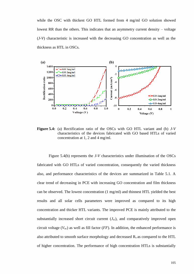
105
while the OSC with thickest GO HTL formed from 4 mg/ml GO solution showed
lowest RR than the others. This indicates that an asymmetry current density – voltage
(J-V) characteristic is increased with the decreasing GO concentration as well as the
thickness as HTL in OSCs.
Figure 5.4: (a) Rectification ratio of the OSCs with GO HTL variant and (b) J-V
characteristics of the devices fabricated with GO based HTLs of varied
concentration at 1, 2 and 4 mg/ml.
Figure 5.4(b) represents the J-V characteristics under illumination of the OSCs
fabricated with GO HTLs of varied concentration, consequently the varied thickness
also, and performance characteristics of the devices are summarized in Table 5.1. A
clear trend of decreasing in PCE with increasing GO concentration and film thickness
can be observed. The lowest concentration (1 mg/ml) and thinnest HTL yielded the best
results and all solar cells parameters were improved as compared to its high
concentration and thicker HTL variants. The improved PCE is mainly attributed to the
substantially increased short circuit current (Jsc), and comparatively improved open
circuit voltage (Voc) as well as fill factor (FF). In addition, the enhanced performance is
also attributed to smooth surface morphology and decreased Rs as compared to the HTL
of higher concentration. The performance of high concentration HTLs is substantially

106
decreased, most likely due to the significant increase in Rs resulting in substantially
lower Jsc and slightly lower transmittance of the film with thickness of ~10 nm,
moreover, Voc and FF also comparatively decreased.
Table 5.1: OSCs photovoltaic performance parameters for GO HTL variants of 1, 2
and 4 mg/ml concentration calculated under illumination and their series
resistance(Rs).
GO HTL
Concentration
Jsc (mA/cm2) Voc (V) FF η (%) Rs(Ω/cm2)
1 mg/ml 8.14 0.80 0.42 2.73 6.89
2 mg/ml 2.90 0.74 0.31 0.67 9.54
4 mg/ml 1.10 0.65 0.31 0.22 11.51
Experimental results show that device fabricated with GO HTL at concentration
of 1mg/ml demonstrated best performance. The optimized thickness of GO HTL is
about 1-3 nm in this work. However, it still lacks the full coverage of ITO and excessive
voids and openings will weaken the charge extraction ability of HTL due to direct
contact of ITO with that of photo-active layer. When high concentration and
consequently thicker HTL is used, the Rs value is observed to increase significantly and
reduce the device performance greatly. Performance of the OSCs fabricated with GO
HTL could be enhanced by optimizing the concentration as well as the surface
morphology and thickness of HTL. In general, an ultrathin GO HTL with full coverage
of ITO surface would yield a high performance. Moreover, we can reduce the band-gap
between GO and photoactive layer by introducing conventional PEDOT:PSS interfacial
layer between GO and PCDTBT:PC71BM photo-active layer to form a bi-layer HTL
structure that would facilitate the transportation of charges towards the ITO.
PEDOT:PSS with the band-gap of 5.1 eV will provide a very good ascending step for
the holes to hop.

107
5.5 Conclusions
In summary, it is demonstrated that the ultrathin GO films (thickness = 1-3 nm)
processed from aqueous dispersion at concentration of 1 mg/ml are a promising
candidate for HTLs in OSCs as compared to their high concentration variant HTLs.
However, HTL concentration and thickness are two critical parameters which are
needed to be optimized for enhanced performance. The decay in device performance is
observed to be mainly driven through a substantial decrease in Jsc and a significant
increase in the Rs values at higher concentrations. Moreover, the Voc, FF and PCE also
reduced as a function of increasing concentration. The efficiency values obtained in our
results are slightly lower than the previously reported data, however, owing to the
advantage of solution processability, nonacidic nature (contrary to PEDOT:PSS),
suitable electrical and optical properties of GO thin films as an HTL indicate its
promising future. For the further optimization of OSCs, development of a novel
composite of GO with that of PEDOT:PSS and metal oxide is currently underway.

108
SIGNIFICANTLY IMPROVED PHOTOVOLTAIC
PERFORMANCE IN POLYMER BULK HETEROJUNCTION
SOLAR CELLS WITH GRAPHENE OXIDE /PEDOT:PSS
DOUBLE DECKED HOLE TRANSPORT LAYER5
6.1 Overview
This work demonstrates the high performance graphene oxide (GO) / PEDOT:PSS
doubled decked hole transport layer (HTL) in the PCDTBT:PC71BM based bulk
heterojunction organic photovoltaic device. The devices were tested on merits of their
power conversion efficiency (PCE), reproducibility, stability and further compared with
the devices with individual GO or PEDOT:PSS HTLs. Solar cells employing
GO/PEDOT:PSS HTL yielded a PCE of 4.28% as compared to either of individual GO
or PEDOT:PSS HTLs where they demonstrated PCEs of 2.77 and 3.57%, respectively.
In case of single GO HTL, an inhomogeneous coating of ITO caused the poor
performance whereas PEDOT:PSS is known to be hygroscopic and acidic which upon
direct contact with ITO reduced the device performance. The improvement in the
photovoltaic performance is mainly ascribed to the increased charge carriers mobility,
short circuit current, open circuit voltage, fill factor, and decreased series resistance.
The well matched work function of GO and PEDOT:PSS is likely to facilitate the
charge transportation and an overall reduction in the series resistance. Moreover, GO
could effectively block the electrons due to its large band-gap of ~ 3.6 eV, leading to an
increased shunt resistance. In addition, the improvement in the reproducibility and
stability has also been observed.
5 The work presented in Chapter 6 has been published in Nature: “Scientific Reports (Rank: Q1, Impact Factor: 5.23)”
as
Rafique et al. (2017). Significantly improved photovoltaic performance in polymer bulk heterojunction solar cells with graphene
oxide/PEDOT:PSS double decked hole transport layer. Scientific Reports, 7(39555), 1-10.

109
6.2 Introduction
Organic photovoltaic devices (OPVs) employing donor-acceptor BHJ structure
are considered promising next generation solar cells due to their advantages over
traditional counterparts, including lower costs, increased flexibility, lighter weight plus
solution processed R2R production compatibility (Kanwat & Jang, 2014; Pan et al.,
2016; Rafique et al., 2016). Although this class of solar cells has seen significant
progress, further development in both efficiency as well as stability are still needed for
their widespread commercial applications (Savagatrup et al., 2015). During recent years,
considerable research has been focused on interfacial engineering of OPVs, in
particular, on the introduction of an interfacial layer between ITO anode and a photo-
active layer that could facilitate the transport of holes, blocking of electrons and reduce
the charge recombination and leakage (Duan et al., 2013; Lattante, 2014). This layer is
often termed as HTL.
PEDOT:PSS is regarded as state of the art HTL which is being used as a
standard material for BHJ OPVs because of its high work function, easy solution
process-ability, high conductivity and high optical transmittance (Lee et al., 2014;
Vitoratos et al., 2009). However, owing to the highly acidic and hygroscopic nature of
PEDOT:PSS, it favors the device degradation in number of ways (Jagadamma et al.,
2014; Norrman et al., 2010). The chemical interaction between PEDOT:PSS and ITO
causes the corrosion of ITO which gives rise to severe instability in device performance
(Ecker et al., 2011). In addition, it absorbs the oxygen and water from the air which
further penetrate to subsequent layers to eventually reduce the device performance
(Kanwat & Jang, 2014). Therefore, research has been focused to either replace or
improve PEDOT:PSS by introducing inorganic semiconductors such as V2O5 (Chen et
al., 2011; Zilberberg et al., 2011), NiO (Wang et al., 2014), WO3 (Chen et al., 2012) or
MoO3, (Xie et al., 2013) among others, to address the reliability issues related to

110
PEDOT:PSS. However, deposition of these oxide materials normally involves intensive
costs related to high vacuum techniques which are incompatible with the large scale roll
to roll OSCs production.
In this context, solution processed aqueous dispersion of GO has been recently
used by several groups as an HTL material for ITO anode (Jeon et al., 2014; Liu et al.,
2012; Stratakis et al., 2014). GO is the derivative of one atom thick graphene comprises
of hydroxyl (OH) and epoxy group on its basal plane and carboxyl groups (COOH) at
the edge (Ding et al., 2015). GO, in aqueous dispersion, exhibits a unique
heterogeneous electronic structure due to the presence of mixed sp2 and sp3
hybridizations (Loh et al., 2010). However, it lacks good Ohmic contact due to its
insulating properties (Yu et al., 2014). Moreover, it is difficult to obtain the full
coverage coating of GO at a time. Therefore, recently combination of GO and
PEDOT:PSS have been reported to effectively work as an HTL in OSCs. It is reported
that use of a thin layer of GO underneath PEDOT:PSS can effectively prevent corrosion
of ITO and its further diffusion into the photoactive layer (Dehsari et al., 2014). Lee et
al. in their recent work on planar heterojunction perovskite solar cells, used
GO/PEDOT:PSS HTL structure to obtain a stable device with power conversion
efficiency (PCE) of 9.74 % (Lee et al., 2016). Similarly, Yu et al. demonstrated highly
efficient polymer light emitting diodes (PLEDs) and OSCs with GO and PEDOT:PSS
composite layer as an HTL (Yu et al., 2014). Park et al. used GO/PEDOT:PSS bi-layer
HTL in P3HT:PCBM based BHJ OSCs and demonstrated a PCE of 3.53% (Park et al.,
2012). In this context, PCDTBT: PC71BM photoactive blend layer in BHJ OSCs has
been used during this study. PCDTBT, as donor polymer, is expected to yield high
efficiency and photo-current generation due to its faster charge carrier generation
capability and different recombination dynamics as compared to P3HT (Banerji et al.,

111
2010; Etzold et al., 2011; Wang et al., 2012). In addition, PCDTBT WF matches well
with that of GO and PEDOT:PSS as compared to P3HT.
In the present study, findings suggest the enhanced efficiency of
PCDTBT:PC71BM based OPVs, using a solution processed GO/PEDOT:PSS double
decked layer as an HTL. It is suggested that combination of GO/PEDOT:PSS as an
HTL may complement the shortcomings of either of individual materials. GO in
combination with PEDOT:PSS as an HTL exhibited a high efficiency and stability as
compared to either of single PEDOT:PSS or GO HTLs. This study investigated the
electrical, optical, chemical and morphological properties and their effects on the
performance of the OPVs.
6.3 Materials and Methods
6.3.1 Materials
PEDOT:PSS aqueous suspension (PH1000) was purchased from H.C. Starck
and used as received. Both PCDTBT and PC71BM have been purchased from Lumtec,
Taiwan. Pre-patterned ITO-coated glass substrates with a sheet resistance of 15 Ω per
square were purchased from Ossila, UK. Graphite flakes has been purchased from
Asbury Inc. (USA). Potassium permanganate (KMnO4, >99%), sulphuric acid (H2SO4,
98%), phosphoric acid (H3PO4, 98%), and hydrochloric acid (HCl, 35%) for GO
synthesis, were obtained from R & M Chemicals. All other necessary chemicals such as
chloroform etc. were purchased commercially and used as received without further
purification.
6.3.2 Synthesis of GO
In the present study, GO was synthesized following a simplified hummers
method (Ming, 2010). Namely, graphite flakes, H3PO4, H2SO4, and KMnO4 were mixed
in an appropriate amount at room temperature by using a magnetic stirrer. The mixture

112
was kept on stirring for about 72 h so that complete oxidation of the graphite could be
achieved. After oxidation of graphite, H2O2 solution along with ice was used to stop the
oxidation. The synthesized GO was subjected to washing for three times with 1 M of
HCl aqueous suspension and several times with DI water to achieve a neutral pH.
During washing process with DI water, the exfoliation of GO was experienced, which
resulted in formation of thick brown GO solution and finally followed by the emergence
of the GO gel. The concentration of obtained GO gel was determined for further studies.
6.3.3 Device Fabrication Procedure
Pre-patterned ITO coated glass substrates were cleaned with consecutive
ultrasonic agitation in acetone, isopropyl alcohol (IPA) and DI water for 20 minutes
each. The substrates after drying with nitrogen stream were subjected to oxygen plasma
treatment to form a hydrophilic surface state. The GO aqueous solution was prepared at
the concentration of 1 mg/ml in DI water, while, PEDOT:PSS solution was filtered by
using 0.45 µm PTFE filters (Whatman, Germany). The doubled decked
(GO/PEDOT:PSS) HTLs were deposited by sequential spin coating of GO and
PEDOT:PSS at 6000rpm for 60 seconds onto the ITO coated substrates and post-
annealed at 150 °C for 5 min in ambient room conditions. For the performance
comparison, individual GO and PEDOT:PSS HTLs were also deposited and annealed at
the same conditions. To perform further fabrication steps, all the materials and
substrates were transferred to nitrogen (N2) filled glove box. To fabricate the photo-
active layer, both PCDTBT (donor) and PC71BM (acceptor) were dissolved in
chloroform at the concentration of 10mg/ml by vigorous stirring overnight and further
mixed at the ratio of 1: 4, respectively. The prepared blend was first filtered by 0.25 µm
PTFE filters and then spun coated at an optimized speed of 2000 rpm for 60 s onto
PEDOT:PSS, GO and GO/PEDOT:PSS HTLs. Next, Al electrodes were thermally
evaporated onto the active layer through shadow masks under vacuum with the pressure

113
of 10-6 Torr. Thereafter, the fabricated devices were encapsulated with glass covering
the active area by using UV-curable epoxy for the characterizations in the air.
6.3.4 Instrumentations
The surface morphologies of the all three types of HTLs were analyzed by
atomic force microscopy (AFM) using tapping mode of Agilent Technologies 5500
Scanning Probe Microscope. Cross-section images were taken by field emission
scanning electrons microscopy (Hitachi, SU8220 Scanning Electron Microscope).
Raman spectra of all types of HTLs were measured by a DXR Raman Microscope
(Thermo Scientific, USA), by using green light excitation (532 nm) laser source with 6
mW power. Optical properties were measured by a Perkin Elmer UV-visible diffuse
reflectance spectrophotometer (Lambda 650) in the range of 250–800 nm. XPS analysis
of prepared GO was carried out by PHI 5000 Versa Probe Scanning ESCA Microprobe
(PHI 5000 Versa Probe II, USA), equipped with monochromatic Al-Kα (hν = 1486.6
eV) X-ray source. The curve fittings for core level spectrum was performed by using
Multipack software (VERSION 9, ULVAC-PHI, Inc. Japan) which allows the
deconvolution of each spectrum into the individual fitting of mixed Gaussian-
Lorentzian components.
Current density-voltage (J-V) characteristics of OPVs were measured using a
Keithley 236 (Keithley Co.) source measurement unit. Photovoltaic performance was
measured by using an Air Mass 1.5 Global (AM 1.5 G) solar simulator with an
irradiation intensity of 100 mW/cm2. The light intensity was calibrated using a Newport
power meter 1918-R with calibrated Si-detector 818-UV.
6.4 Results and Discussion
In the present study, the BHJ OPVs were fabricated with single GO,
PEDOT:PSS and double decked GO/PEDOT:PSS as HTLs. GO possesses several

114
unique advantages, including its tunable energy levels, facile solution processed, low
cost synthesis, its two-dimensional structure and easy functionalization(Liu et al.,
2014). However, it is essential to fully cover the ITO surface with a uniform and very
thin layer to achieve an optimum performance with a GO HTL. Moreover, post
deposition annealing is also recommended to remove the oxygen function groups and
consequently the electrical properties of GO could be improved (Jeon et al., 2014). It is
difficult to deposit highly uniform thin layer of GO with full coverage of ITO surface.
As a result, poor holes extraction to ITO anode can be expected because of the direct
contact of BHJ photo-active layer with the ITO at the uncovered regions. In addition,
non-uniform surface coverage by GO may also lead to inhomogeneous electrical
properties yielding a poor reliability of the device performance (Lee et al., 2016).
Similarly, standard PEDOT:PSS HTL also exhibits severe stability issues. To address
these point, low temperature (150 °C) solution processed approach to fabricate BHJ
OPVs with sequential spin coating of GO and PEDOT:PSS was used and compared
with that of individual GO or PEDOT:PSS HTLs on merit of their efficiency,
reproducibility and stability. The schematic of the current work is presented in Figure
6.1.

115
Figure 6.1: (a) Schematic illustration of the BHJ OPVs with GO, PEDOT:PSS and
GO/PEDOT:PSS HTLs and (b) The energy band diagram showing the
energy levels of all the materials used in OPVs of current study.
6.4.1 Spectroscopic Characterizations
The optical and structural properties of each HTL deposited on ITO coated glass
substrates have been investigated prior to device fabrication. Transmittance spectra of
all three types of HTLs along with bare ITO are shown in Figure 6.2(a). These layers
show high transmittance in the overall wavelength range of more than 87%. The optical
transparency of HTLs is very important in order to absorb maximum light by photo-
active layer. It can be observed that the transmittance spectra of the ITO/PEDOT:PSS
and ITO/GO/PEDOT:PSS is almost 15% higher compared with the transmittance of
pristine ITO and ITO/GO in the region of ~ 400-500 nm. However, no pronounced
change in transmittance spectra for any of the HTLs is observed in the overall
wavelength region except the aforementioned wavelength range. The observed
difference of transmittance in the ~ 400-500 nm region could potentially bring a
significant effect on the photo-generated current (Jsc) of the device and hence the better

116
efficiency is expected in case of ITO/PEDOT:PSS and ITO/GO/PEDOT:PSS, in good
agreement with the photovoltaic studies of the corresponding devices.
Raman spectroscopy is the most commonly used non-destructive technique to
analyze the quality and structure of the carbon based materials, in particular, it is being
used to investigate the defects and ordered and disordered structures of graphene (Some
et al., 2013). Raman spectrum was collected for GO/PEDOT:PSS double decked
structure as shown in Figure 6.2(b). For comparison, the spectra of single GO and
PEDOT:PSS HTLs were also collected. Raman spectrum for single GO HTL shows
both D and G bands appearing at 1350 and 1600 cm-1, respectively. It is well known that
D band appearing in the range of 1200 to 1500 cm-1 corresponds to structural defects
and partially disordered structures of the sp2 domains, whereas, G band appearing from
1500 to 1600 cm-1 is associated with E2g - vibration mode of sp2 carbon (Some et al.,
2013; Zhang et al., 2014). The wide band towards high frequency end of the spectrum
features three peaks at around 2720, 2930 and 3190 cm-1. The peak at 2790 cm-1 is
corresponding to an overtone of D band and attributed as 2D band, whereas, the peak at
2930 cm-1 arise from contribution of both D and G bands and often termed as D+G band
(Bajpai et al., 2012; Delgado et al., 2008). The shoulder peak at ~ 3190 cm-1 also
ascribes to an overtone of D band (2D). The Raman spectrum for GO/PEDOT:PSS
films also illustrated D and G bands but with significantly decreased intensity of the
peaks as shown in Figure 6.2b. In addition, the spectrum is featured with some bands
from PEDOT:PSS polymer in low frequency range between 500 to 1100 cm-1 which
confirms the method efficacy of double decked layer fabrication. The GO/PEDOT:PSS
HTL also features the 2D, D+G and 2D bands at 2700, 2930 and 3170 cm-1 but with
significantly low intensity as compared to pure GO films. The Raman spectrum for
PEDOT:PSS HTL shown in Figure 6.2(c) exhibits Raman finger prints for PEDOT and
PSS. Most of the peaks are attributed to PEDOT and negligible contribution of PSS is

117
observed in the spectrum, in good agreement with previously reported data (Rafique et
al., 2016; Sakamoto et al., 2005). A strong vibrational band observed at 1440 cm-1 is
attributed to PEDOT and related to symmetric Cα = Cβ (- O) stretching mode. In
addition, the following bands are related to PEDOT vibrational modes such as: 1562
cm-1 is ascribed to Cα = Cβ asymmetrical stretching, 1364 cm-1 to Cβ - Cβ stretching
deformations and 1255 cm-1 to Cα - Cα inter-ring stretching vibrations (Chang et al.,
2014; Farah et al., 2012). The peaks at 986 and 573 cm-1 correspond to the oxyethylene
ring deformation (Teng et al., 2013).
Figure 6.2: (a) Transmittance of GO, PEDOT:PSS and GO/PEDOT:PSS films
deposited on ITO coated substrate and that of bare ITO substrate.
(b) Raman spectra for GO, GO/PEDOT:PSS and (c) PEDOT:PSS HTLs.
(d) Deconvoluted XPS C 1s spectrum of GO.

118
The core level XPS C 1s spectrum of the GO presented in Figure 6.2(d) is
decomposed into two components, the sharp and high intensity peak at 284.7 eV is
ascribed to sp2 carbon aromatic rings (C-C/C=C) and relatively low intensity peak at
286.1 eV corresponds to C-O bond (Some et al., 2013; Wang et al., 2014). These peaks
confirm the presence of carbon atoms in different functional groups , i.e. the non-
oxygenated rings and oxygen related functional groups (Kim et al., 2015; Some et al.,
2012).
6.4.2 Morphological Study of HTLs
Film morphology of an HTL significantly influences the electrical properties of
the device, in particular, the Rs and shunt resistance (Rsh). In general, a smooth and
fully-covered HTL morphology may induce a higher Rsh and low Rs which is highly
desirable to enhance the performance of OSCs (Jeon et al., 2014). It is therefore vital to
control the morphology of the HTLs. In the present study, the AFM topography images
of the all three HTLs on ITO were taken as shown in Figure 6.3. RMS roughness values
of GO, PEDOT:PSS and GO/PEDOT:PSS films in an area of 5 µm × 5µm were
calculated to be 2.88, 1.56 and 1.99 nm, respectively. As compared to the recently
reported results (3.2 nm) for spin coated GO films (Lee et al., 2016), the RMS
roughness of our samples is comparatively improved but it is still significantly higher
than PEDOT:PSS HTL. The single GO HTL is inhomogeneous with overlapping GO
flakes across the surface as visible in AFM image (Figure 6.3(a)) and could not cover
the ITO surface with high uniformity. Consequently, the non-uniform and overlapping
GO flakes could suppress the transportation of holes while the uncovered areas may
lead to direct contact of ITO and photo-active layer and hence the performance of OSCs
with GO as HTLs could significantly reduce (Ding et al., 2015). By applying
PEDOT:PSS on GO (GO/PEDOT:PSS HTL), RMS roughness reduced to 1.99 nm

119
(Figure 6.3e), comparable with single PEDOT:PSS (Figure 6.3c), which indicate that
deposition of PEDOT:PSS on GO results in smoothening of the irregular GO surface.
Figure 6.3: The AFM surface topography images and SEM cross-sectional images
with complete device, of (a, b) GO (c, d) PEDOT:PSS and
(e, f) GO/PEDOT:PSS HTLs.

120
Figure 6.3 shows cross-sectional SEM images of the solar cells fabricated with
each of the GO, PEDOT:PSS (Figure 6.3d) and GO/PEDOT:PSS (Figure 6.3f) HTLs.
The thickness of PCDTBT:PC71BM were observed to be uniform (approx. 75 nm)
regardless of the HTLs. The single GO film was very thin (around 1-3 nm) to
distinguish as shown in Figure 6.3(c). The thickness of both PEDOT:PSS and
GO/PEDOT:PSS HTLs was approximately the same and calculated to be around 30 nm.
6.4.3 Photovoltaic Characteristics
In order to analyze the photovoltaic characteristics, it is important to explain the
role of HTL during the OPVs operation. In normal architecture BHJ OSCs, the photo-
active layer is irradiated with solar light via ITO/HTL bottom electrode side, while the
active layer absorbs the solar light (photons) and generates electrons- holes pairs, the so-
called excitons. Further, these excitons dissociate into the electrons in the lowest
unoccupied molecular orbital (LUMO) and holes in the highest occupied molecular
orbital (HOMO), at the donor-acceptor interface. Therefore, the HOMO level of the
donor polymer should match well with the work-function of HTL to facilitate the
transportation of holes through HTLs to the anode (Stratakis et al., 2014). In this
context, PCDTBT with the HOMO of 5.3 eV was utilized along with the
GO/PEDOT:PSS HTL. The device with PCDTBT as donor polymer provides better
holes extraction since energy levels from PCDTBT/ PEDOT:PSS/ GO/ ITO provide
good ascending steps for the holes to hop. The energy level diagram for each element
used in this study and the device structure is presented in Figure 6.1. Reference devices
with only GO and PEDOT:PSS as an HTL were also fabricated for comparison. In
addition, the performance of GO is somehow thickness dependent and one can achieve
an optimum performance with the GO layer of 1-3 nm (Li et al., 2010). Therefore, the
thickness and concentration of GO were optimized, and with the spinning conditions

121
described in the experimental section, a layer of approximately 1-3 nm was obtained as
shown in Figure 6.4(a).
Figure 6.4(b) shows the typical current density-voltage (J-V) characteristics
under illumination of the PCDTBT:PC71BM OSC devices with GO, PEDOT:PSS and
GO/PEDOT:PSS as the HTLs, and the corresponding extracted device parameters are
summarized in Table 6.1. As shown in J-V curves, the devices using the
GO/PEDOT:PSS double decked HTL showed superior performance as compared to the
individual GO or PEDOT:PSS HTLs with a Voc of 0.82 V, a Jsc of 10.44 mA/cm2 , FF of
0.50 and a PCE (η) of 4.28 %. In comparison, the devices with only PEDOT:PSS as an
HTL exhibited a relatively low performance with Voc of 0.80 V, a Jsc of 9.49 mA/cm2, a
FF of 0.47 and an η of 3.57 %. Whereas, the device with single GO exhibited poor
performance with a Voc of 0.80 V, a Jsc of 7.90 mA/cm2, a FF of 0.44 and a PCE of
2.77 %. Relatively poor performance of the devices with individual GO HTL is mainly
attributed to inhomogeneous GO layer with high surface roughness that lead to
suppression and an inefficient transportation of holes. As a result, the device efficiency
is significantly reduced. For the devices based on GO/PEDOT:PSS HTL, the
improvement is attributable to high Jsc, FF and Voc values as compared to either of GO
or PEDOT:PSS HTLs. Additionally, the GO/PEDOT:PSS HTL also exhibited reduced
Rs than GO or PEDOT:PSS single HTLs, as shown in Figure 6.4(c). Relatively low Rs
value in case of GO/PEDOT:PSS HTL suggest the better charge transportation ability
of the double decked structure as compared to single GO and PEDOT:PSS based
devices. As discussed above and presented in the energy diagram in Figure 6.1, the WF
of GO (4.9 eV) matches well with PEDOT:PSS (5.1 eV) which likely results in an
efficient charge extraction and transportation to ITO. Moreover, GO could effectively
block the electrons owing to its large band-gap of ~ 3.6 eV (Lee et al., 2016).

122
Table 6.1: Device photovoltaic performance characteristics of PCDTBT:PC71BM
OPVs incorporating GO, PEDOT:PSS and GO/PEDOT:PSS as the HTLs.
Anode interlayer Jsc (mA/cm2) Voc (V) FF Mobility, μ
(cm2/Vs)
η (%)
GO 7.90 0.80 0.44 4.04 x 10⁻⁴ 2.77
PEDOT:PSS 9.49 0.80 0.47 3.78 x 10⁻⁴ 3.57
GO/PEDOT:PSS 10.44 0.82 0.50 7.47 x 10⁻⁴ 4.28
Figure 6.4: (a) Thickness vs concentration plots for GO. (b) J-V characteristics of
OPVs with GO, PEDOT:PSS and GO/PEDOT:PSS as an HTL. (c) Rsh and
Rs calculated from J-V curves under illumination conditions. (d) Stability
test of OPVs over 250 h.
Since operational stability of the OPVs is one of the most important factors for
their widespread commercialization, therefore, the operational stability of all type of
HTLs was explored. Figure 6.4(d) shows the decay in PCE as a function of exposure

123
time in ambient atmosphere. The devices with single GO HTLs or with
GO/PEDOT:PSS HTLs showed better stability as compared to single PEDOT:PSS
HTLs in which the efficiency decreased to more than 50% of initial value. The
instability in the PEDOT:PSS HTL is attributed to corrosion of indium due to acidic
nature of PEDOT:PSS with high pH value (Wong et al., 2002). With the passage of
time indium diffuses into the HTL and further to active layer which causes severe
damage to the device performance. The improved stability in case of single
GO/PEDOT:PSS HTL is expected because a thin layer of GO underneath PEDOT:PSS
serves as a barrier against the direct contact of PEDOT:PSS with ITO surface.
The effective carrier mobility or the so-called ambipolar mobility for all three
devices was then determined by space-charge-limited-current (SLCL) method under
positive voltage up to 10 V in dark. Figure 6.5 shows log J vs. log V, several conduction
regimes have been identified from the plots based on their gradient values, such as:
I ~ V1 with slope 1 is an Ohmic regime, I ~ V2 with slope 2 is an SCLC regime, while
I > V2 with slope > 2 is a trap regime. The ambipolar mobility has been calculated from
the SCLC regime by the following equation:
𝐽 = 9
8𝜀𝜀𝑜𝜇
𝑉2
𝐿3 …………………………………………. (6.1)
Where J is the current density within the conduction regime, ε is the relative
dielectric constant, εo is the vacuum permittivity, L is the active layer thickness, V the
voltage within the conduction regime and μ represents the mobility (Yang et al., 2012).
Figure 6.5 and Table 6.1 show the change of ambipolar mobility for the devices with
GO, PEDOT:PSS and GO/PEDOT:PSS HTLs. The ambipolar mobility increased from
3.78 x 10⁻⁴ cm2 V-1 s-1 in case of PEDOT:PSS HTL to 4.04 x 10⁻⁴ cm2 V-1 s-1 for single
GO HTL and finally to 7.47 x 10⁻⁴ cm2 V-1 s-1 for the device with GO/PEDOT:PSS
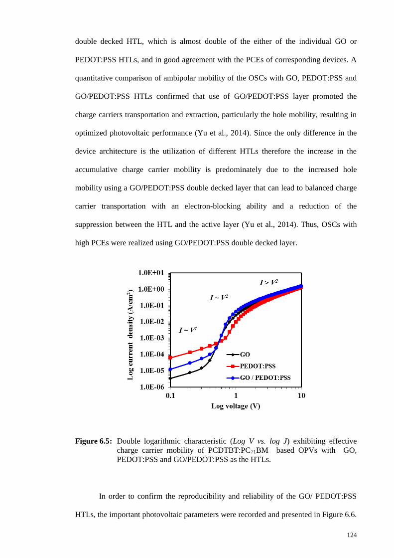
124
double decked HTL, which is almost double of the either of the individual GO or
PEDOT:PSS HTLs, and in good agreement with the PCEs of corresponding devices. A
quantitative comparison of ambipolar mobility of the OSCs with GO, PEDOT:PSS and
GO/PEDOT:PSS HTLs confirmed that use of GO/PEDOT:PSS layer promoted the
charge carriers transportation and extraction, particularly the hole mobility, resulting in
optimized photovoltaic performance (Yu et al., 2014). Since the only difference in the
device architecture is the utilization of different HTLs therefore the increase in the
accumulative charge carrier mobility is predominately due to the increased hole
mobility using a GO/PEDOT:PSS double decked layer that can lead to balanced charge
carrier transportation with an electron-blocking ability and a reduction of the
suppression between the HTL and the active layer (Yu et al., 2014). Thus, OSCs with
high PCEs were realized using GO/PEDOT:PSS double decked layer.
Figure 6.5: Double logarithmic characteristic (Log V vs. log J) exhibiting effective
charge carrier mobility of PCDTBT:PC71BM based OPVs with GO,
PEDOT:PSS and GO/PEDOT:PSS as the HTLs.
In order to confirm the reproducibility and reliability of the GO/ PEDOT:PSS
HTLs, the important photovoltaic parameters were recorded and presented in Figure 6.6.

125
The GO/ PEDOT:PSS HTL exhibited fairly good reproducibility with minor variations
in Voc, Jsc and PCE. On the contrary, the device with GO HTL showed comparatively
wide variations in Voc. However, a relatively wider variation is observed in FF of all
HTLs which could be attributed to the absence of ETL in our device structure.
Figure 6.6: Photovoltaic performance parameters including (a) Jsc , (b) Voc , (c) FF and
(d) PCEs (%) of PCDTBT:PC71BM based OPVs with GO, PEDOT:PSS
and GO/PEDOT:PSS as the HTLs.
The selection of double decked GO/PEDOT:PSS HTL played a vital role in the
improved device efficiency and stability. It has been reported that use of either of
individual GO or PEDOT:PSS as HTLs in OPVs may cause severe instability issues at
the anode interface (Jørgensen et al., 2012; Lee et al., 2016).The hygroscopic and acidic
PEDOT:PSS aqueous suspension could react with both the ITO as well as the
photoactive layer. Similarly, single and ultrathin GO layer could cause a non-uniform

126
coating on ITO which would provide a direct contact of ITO and photoactive layer at
the non-covered regions and drastically reduces the device performance. Interestingly,
the combination of GO and PEDOT:PSS in a double decked structure is a compatible
solution to compliment the drawbacks of both individual materials. To the best of my
knowledge, there is no report on photovoltaic performance, reproducibility and stability
of PCDTBT:PC71BM based devices with GO/ PEDOT:PSS double decked layer.
6.5 Conclusions
In summary, the performance, reproducibility and stability of GO/PEDOT:PSS
double decked hole transport layers in PCDTBT:PC71BM based OPVs are reported. The
GO/PEDOT:PSS is a promising candidate to replace conventional PEDOT:PSS or
single GO HTLs by complimenting the drawbacks of both individual materials. The
GO/PEDOT:PSS HTL retained its efficiency as well as reproducibility yielding a highly
stable device. It demonstrated a Jsc = 10.44 mA/cm2, Voc = 0.82 V, FF =0.50, and PCE =
4.28 %. A well matched work function of GO/PEDOT:PSS = 4.9 eV/5.1 eV with that
of PCDTBT (5.3 eV) donor material facilitates the hole transportation to ITO. The
improved performance is also attributed to decreased Rs which are highly desired for
carrier transportation and collection as evident from charge carrier’s mobility results.
Moreover, the high Rsh of GO also helps to suppress carrier recombination. Both
parameters were calculated from J-V curves. GO is probably inducing effective
blocking of electron due to its large band gap of ~ 3.6 eV. In addition to the reasonably
improved efficiency, reproducibility and stability, the preparation of HTLs as well as
photoactive layer are based on a facile, flexible and R2R compatible solution process,
which remarkably simplifies the overall fabrication process and lowers the fabrication
cost.
127
CONCLUSIONS AND FUTURE CHALLANGES.
7.1 Conclusions
Organic photovoltaic materials open up the new pathways to develop solar cells
modules based on a facile, solution processable and R2R compatible fabrication
techniques. However, like any burgeoning OSC related technology there are several
instability issues that need to be addressed to move beyond the laboratory. The biggest
obstacles in their widespread commercialization are their low efficiencies and shorter
life time as compared to that of already developed technologies. In this context, this
PhD thesis successfully describes the degradation factors effecting device stability, and
performance achievements of OSCs by overcoming the stability issues associated with
the HTL. One crucial step was the identification of the degradation factors pertaining to
device instability in ambient air, in particular related to the HTL. Further to address
those factors by introducing organic-inorganic hybrid HTLs consisting of conventional
PEDOT:PSS material along with V2O5 and/or GO. Moreover, a range of
characterization techniques were presented, which have been used in the current work.
It was shown that many characteristics such as device architecture, material
combinations, ITO diffusion, oxygen ingress, concentration ratios and layer thicknesses
can significantly affect the device performance. During this work, the overarching
theme was to study metal oxides (V2O5) and/or GO in HTL of BHJ OSCs with the aim
to ensure utilization of a facile, flexible, low cost and R2R compatible solution process,
which remarkably simplifies the overall fabrication process. This dissertation can be
subdivided into three major sections. A summary of each of the section is presented
here followed by a brief outlook of the future challenges and strategies to follow-up the
present work.

128
In the first step, stability and degradation issues pertaining to each layer of the
normal architecture BHJ OSCs as a function of exposure time to ambient air were
discussed. The BHJ OSCs were fabricated and their photovoltaic performance was
evaluated. It was shown, that indium and oxygen diffusion are one of the main causes of
device degradation which cause deterioration of chemical, optical, morphological and
photovoltaic characteristics of the device. This study was mainly focused on identifying
and addressing the stability constraints brought by PEDOT:PSS due to its acidic nature
and instability issues due to device exposure in ambient atmosphere.
In the second set of experiments, the stability issues associated with the
PEDOT:PSS were addressed, by incorporating V2O5 nanoparticles in the PEDOT:PSS
HTL to develop an organic-inorganic hybrid HTL. The resultant device has significant
improvement in stability while maintaining the efficiencies comparable to that of
pristine PEDOT:PSS HTL.
In the third section, GO was utilized as an HTL in the PCDTBT:PC71BM based
BHJ OSCs. At first, the GO concentration was optimized for the best photovoltaic
performance. Further, the optimized concentration was utilized as an under-layer in GO/
PEDOT:PSS double decked HTL. The resultant devices were tested on the merits of
their stability, efficiency and reproducibility and compared with those containing either
of GO or PEDOT:PSS HTLs. The device with double decked HTL has successfully
overcome the drawbacks of any of the individual GO or PEDOT:PSS HTL.
In conclusion, we optimized the fabrication parameters by adopting a facile and
solution processable fabrication process by simply spin coating of HTL as well as
photoactive layer. Degradation factors, particularly in context of HTL, were identified
and successfully addressed by employing V2O5 and GO based HTLs. Moreover, the

129
operational stability of the OSCs have been remarkably improved by employing hybrid
HTLs as compared to pristine PEDOT:PSS HTLs.
7.2 Future Challenges
There are a number of challenges that still need to be addressed to accomplish
the current work, which were not possible to do within the frames of this study. In
particular:
a) Further studies of metal oxides and/or GO have to be carried out to develop
optimized processing conditions of the layers for the manufacturing of
efficient OSCs. These optimized fabrication conditions for the metal oxides
and/or GO can be implemented to manufacture tandem solar cells.
b) Degradation studies should be extended to develop optimized atmospheric
chambers for an in-depth analysis of degradation factors such as humidity,
oxygen, and electrode corrosion and diffusion etc.
c) Several important points should be addressed pertaining to device
fabrication, stability and degradation study such as, improved buffered
layers, proper encapsulation, high efficiency and stability, increased
geometrical FF and fabrication of large scale R2R solar cell modules.

130
REFERENCES
Aluicio-Sarduy, E., Baidak, A., Vougioukalakis, G. C., & Keivanidis, P. E. (2014).
Phosphorimetric characterization of solution-processed polymeric oxygen
barriers for the encapsulation of organic electronics. The Journal of Physical
Chemistry C, 118(5), 2361-2369.
Ameen, M. Y., Pradhan, S., Suresh, M. R., & Reddy, V. (2015). MoO3 anode buffer
layer for efficient and stable small molecular organic solar cells. Optical
Materials, 39, 134-139.
Ameri, T., Dennler, G., Lungenschmied, C., & Brabec, C. J. (2009). Organic tandem
solar cells: A review. Energy & Environmental Science, 2(4), 347-363.
Ameri, T., Khoram, P., Min, J., & Brabec, C. J. (2013). Organic ternary solar cells: A
review. Advanced Materials, 25(31), 4245-4266.
An, Q., Zhang, F., Zhang, J., Tang, W., Deng, Z., & Hu, B. (2016). Versatile ternary
organic solar cells: A critical review. Energy & Environmental Science, 9(2),
281-322.
Anderson, D., Goldemberg, J., & Johansson, T. B. (2004). World Energy Assessment:
Overview: 2004 Update: United Nations Publications.
Armin, A., Velusamy, M., Wolfer, P., Zhang, Y., Burn, P. L., Meredith, P., & Pivrikas,
A. (2014). Quantum efficiency of organic solar cells: Electro-optical cavity
considerations. ACS Photonics, 1(3), 173-181.
Aslam, M., Ismail, I. M., Salah, N., Chandrasekaran, S., Qamar, M. T., & Hameed, A.
(2015). Evaluation of sunlight induced structural changes and their effect on the
photocatalytic activity of V2O5 for the degradation of phenols. Journal of
Hazardous Materials, 286, 127-135.
Awartani, O., Lemanski, B. I., Ro, H. W., Richter, L. J., DeLongchamp, D. M., &
O'Connor, B. T. (2013). Correlating stiffness, ductility, and morphology of
polymer: fullerene films for solar cell applications. Advanced Energy Materials,
3(3), 399-406.
Aygul, U., Hintz, H., Egelhaaf, H.-J., Distler, A., Abb, S., Peisert, H., & Chasse, T.
(2013). Energy level alignment of a P3HT/fullerene blend during the Initial
steps of degradation. The Journal of Physical Chemistry C, 117(10), 4992-4998.
Badawy, W. A. (2015). A review on solar cells from Si-single crystals to porous
materials and quantum dots. Journal of Advanced Research, 6(2), 123-132.
Bagnall, D. M., & Boreland, M. (2008). Photovoltaic technologies. Energy Policy,
36(12), 4390-4396.
Bailo, D., Generosi, A., Albertini, V. R., Caminiti, R., De Bettignies, R., & Paci, B.
(2012). Time-resolved morphological study of ‘PEDOT:PSS’hole transporting
layer for polymer solar cells. Synthetic Metals, 162(9), 808-812.
131
Bajpai, R., Roy, S., Rafiee, J., Koratkar, N., & Misra, D. (2012). Graphene supported
nickel nanoparticle as a viable replacement for platinum in dye sensitized solar
cells. Nanoscale, 4(3), 926-930.
Banerji, N., Cowan, S., Leclerc, M., Vauthey, E., & Heeger, A. J. (2010). Exciton
formation, relaxation, and decay in PCDTBT. Journal of the American Chemical
Society, 132(49), 17459-17470.
Bao, Q., Liu, X., Braun, S., & Fahlman, M. (2014). Oxygen‐and water‐based
degradation in [6, 6]‐phenyl‐C61‐butyric acid methyl ester (PCBM) films.
Advanced Energy Materials, 4(6). 1301272- 1301278.
Baranovskii, S., Cordes, H., Hensel, F., & Leising, G. (2000). Charge-carrier transport
in disordered organic solids. Physical Review B, 62(12), 7934- 7938.
Bekci, D. R., & Erten-Ela, S. (2012). Effect of nanostructured ZnO cathode layer on the
photovoltaic performance of inverted bulk heterojunction solar cells. Renewable
Energy, 43, 378-382.
Bhushan, B. (2012). Fundamentals of tribology and bridging the gap between the
macro-and micro/nanoscales (Vol. 10): Springer Science & Business Media.
Bin Mohd Yusoff, A. R., Kim, H. P., & Jang, J. (2014). High performance organic
photovoltaics with zinc oxide and graphene oxide buffer layers. Nanoscale, 6(3),
1537-1544.
Blom, P. W., Mihailetchi, V. D., Koster, L. J. A., & Markov, D. E. (2007). Device
physics of polymer: fullerene bulk heterojunction solar cells. Advanced
Materials, 19(12), 1551-1566.
Blouin, N., Michaud, A., & Leclerc, M. (2007). A low‐bandgap poly (2, 7‐carbazole)
derivative for use in high‐performance solar cells. Advanced Materials, 19(17),
2295-2300.
Brabec, C. J., Cravino, A., Meissner, D., Sariciftci, N. S., Fromherz, T., Rispens, M. T.,
& Hummelen, J. C. (2001). Origin of the open circuit voltage of plastic solar
cells. Advanced Functional Materials, 11(5), 374-380.
Brabec, C. J., Winder, C., Sariciftci, N. S., Hummelen, J. C., Dhanabalan, A., van Hal,
P. A., & Janssen, R. A. (2002). A low-bandgap semiconducting polymer for
photovoltaic devices and infrared emitting diodes. Advanced Functional
Materials, 12(10), 709-712.
Bronstein, H., Chen, Z., Ashraf, R. S., Zhang, W., Du, J., Durrant, J. R., . . & Geerts, Y.
(2011). Thieno [3, 2-b] thiophene− diketopyrrolopyrrole-containing polymers
for high-performance organic field-effect transistors and organic photovoltaic
devices. Journal of the American Chemical Society, 133(10), 3272-3275.
Brown, G. F., & Wu, J. (2009). Third generation photovoltaics. Laser & Photonics
Reviews, 3(4), 394-405.

132
Bruner, C., Miller, N. C., McGehee, M. D., & Dauskardt, R. H. (2013). Molecular
intercalation and cohesion of organic bulk heterojunction photovoltaic devices.
Advanced Functional Materials, 23(22), 2863-2871.
Bruner, C., Novoa, F., Dupont, S., & Dauskardt, R. (2014). Decohesion kinetics in
polymer organic solar cells. ACS Applied Materials & Interfaces, 6(23), 21474-
21483.
Bulavko, G., & Ishchenko, A. A. (2014). Organic bulk heterojunction photovoltaic
structures: design, morphology and properties. Russian Chemical Reviews,
83(7), 575.
Bulle-Lieuwma, C., Van Gennip, W., Van Duren, J., Jonkheijm, P., Janssen, R., &
Niemantsverdriet, J. (2003). Characterization of polymer solar cells by TOF-
SIMS depth profiling. Applied Surface Science, 203, 547-550.
Burlingame, Q., Tong, X., Hankett, J., Slootsky, M., Chen, Z., & Forrest, S. R. (2015).
Photochemical origins of burn-in degradation in small molecular weight organic
photovoltaic cells. Energy & Environmental Science, 8(3), 1005-1010.
Cai, W., Gong, X., & Cao, Y. (2010). Polymer solar cells: recent development and
possible routes for improvement in the performance. Solar Energy Materials
and Solar Cells, 94(2), 114-127.
Campos-Delgado, J., Romo-Herrera, J. M., Jia, X., Cullen, D. A., Muramatsu, H., Kim,
Y. A., & Okuno, Y. (2008). Bulk production of a new form of sp 2 carbon:
crystalline graphene nanoribbons. Nano Letters, 8(9), 2773-2778.
Campoy-Quiles, M., Ferenczi, T., Agostinelli, T., Etchegoin, P. G., Kim, Y.,
Anthopoulos, T. D., & Nelson, J. (2008). Morphology evolution via self-
organization and lateral and vertical diffusion in polymer:fullerene solar cell
blends. Nature Materials, 7(2), 158-164.
Cao, B., He, X., Fetterly, C. R., Olsen, B. C., Luber, E. J., & Buriak, J. M. (2016). Role
of interfacial layers in organic solar cells: Energy level pinning versus phase
segregation. ACS Applied Materials & Interfaces, 8(28), 18238-18248.
Cao, H., He, W., Mao, Y., Lin, X., Ishikawa, K., Dickerson, J. H., & Hess, W. P.
(2014). Recent progress in degradation and stabilization of organic solar cells.
Journal of Power Sources, 264, 168-183.
Chandrasekaran, J., Nithyaprakash, D., Ajjan, K., Maruthamuthu, S., Manoharan, D., &
Kumar, S. (2011). Hybrid solar cell based on blending of organic and inorganic
materials—An overview. Renewable and Sustainable Energy Reviews, 15(2),
1228-1238.
Chang, C.-H., & Chen, S.-A. (2007). Effect of ionization potential change in poly (3, 4-
ethylenedioxythiophene): poly (styrenesulfonic acid) on the performance of
polymer light emitting diodes due to its reaction with indium tin oxide. Applied
Physics Letters, 91(10), 103514-103516.
133
Chang, S. H., Chiang, C.-H., Kao, F.-S., Tien, C.-L., & Wu, C.-G. (2014a). Unraveling
the enhanced electrical conductivity of PEDOT:PSS thin films for ITO-free
organic photovoltaics. IEEE Photonics Journal, 6(4), 1-7.
Chen, C. C., Chang, W. H., Yoshimura, K., Ohya, K., You, J., Gao, J., & Yang, Y.
(2014). An efficient triple‐junction polymer solar cell having a power
conversion efficiency exceeding 11%. Advanced Materials, 26(32), 5670-5677.
Chen, C. P., Chen, Y. D., & Chuang, S. C. (2011). High‐performance and highly
durable inverted organic photovoltaics embedding solution‐processable
vanadium oxides as an interfacial hole‐transporting layer. Advanced Materials,
23(33), 3859-3863.
Chen, C. P., Huang, C. Y., & Chuang, S. C. (2015). Highly thermal stable and efficient
organic photovoltaic cells with crosslinked networks appending open‐cage
fullerenes as additives. Advanced Functional Materials, 25(2), 207-213.
Chen, L., Tian, S., & Chen, Y. (2014). Enhanced performance for organic bulk
heterojunction solar cells by cooperative assembly of ter (ethylene oxide)
pendants. Polymer Chemistry, 5(15), 4480-4487.
Chen, M.-C., Chiou, Y.-S., Chiu, J.-M., Tedla, A., & Tai, Y. (2013). Marked
improvement in the stability of small molecule organic photovoltaics by
interfacial modification using self-assembled monolayers to prevent indium
diffusion into the active layer. Journal of Materials Chemistry A, 1(11), 3680-
3687.
Chen, S., Manders, J. R., Tsang, S.-W., & So, F. (2012). Metal oxides for interface
engineering in polymer solar cells. Journal of Materials Chemistry, 22(46),
24202-24212.
Chen, Z., Deutsch, T. G., Dinh, H. N., Domen, K., Emery, K., Forman, A. J., &
Jaramillo, T. F. (2013). Incident photon-to-current efficiency and photocurrent
spectroscopy. Photoelectrochemical Water Splitting (pp. 87-97): Springer.
Cheng, C.-E., Tsai, C.-W., Lin, T.-W., Pei, Z., Chang, C.-S., & Chien, F. S.-S.(2014).
Graphene oxide as hole transport layers for P3HT:PCBM solar cells. In
Conference IX: Photovoltaic Technology, Optic.
Cheng, C.-E., Tsai, C.-W., Pei, Z., Lin, T.-W., Chang, C.-S., & Chien, F. S.-S. (2015).
UV-treated graphene oxide as anode interfacial layers for P3HT: PCBM solar
cells. Journal of Physics D: Applied Physics, 48(25), 255103-255110.
Cheng, P., & Zhan, X. (2016). Stability of organic solar cells: Challenges and strategies.
Chemical Society Reviews, 45(9), 2544-2582.
Cheng, Y.-J., Yang, S.-H., & Hsu, C.-S. (2009). Synthesis of conjugated polymers for
organic solar cell applications. Chemical Reviews, 109(11), 5868-5923.
Cheng, Y. J., Hsieh, C. H., Li, P. J., & Hsu, C. S. (2011). Morphological stabilization by
in situ polymerization of fullerene derivatives leading to efficient, thermally
stable organic photovoltaics. Advanced Functional Materials, 21(9), 1723-1732.

134
Cho, S.-P., Yeo, J.-S., Kim, D.-Y., Na, S.-i., & Kim, S.-S. (2015). Brush painted V2O5
hole transport layer for efficient and air-stable polymer solar cells. Solar Energy
Materials and Solar Cells, 132, 196-203.
Cho, S., Seo, J. H., Park, S. H., Beaupré, S., Leclerc, M., & Heeger, A. J. (2010). A
thermally stable semiconducting polymer. Advanced Materials, 22(11), 1253-
1257.
Choi, H., Kim, B., Ko, M. J., Lee, D.-K., Kim, H., Kim, S. H., & Kim, K. (2012).
Solution processed WO3 layer for the replacement of PEDOT:PSS layer in
organic photovoltaic cells. Organic Electronics, 13(6), 959-968.
Choi, H., Mai, C.-K., Kim, H.-B., Jeong, J., Song, S., Bazan, G. C., & Heeger, A. J.
(2015). Conjugated polyelectrolyte hole transport layer for inverted-type
perovskite solar cells. Nature Communications, 6(7358),1-6.
Chou, T.-R., Chen, S.-H., Chiang, Y.-T., Lin, Y.-T., & Chao, C.-Y. (2015). Highly
conductive PEDOT:PSS film by post-treatment with dimethyl sulfoxide for
ITO-free liquid crystal display. Molecular Crystals and Liquid Crystals, 612(1),
201-210.
Chueh, C.-C., Li, C.-Z., & Jen, A. K.-Y. (2015). Recent progress and perspective in
solution-processed interfacial materials for efficient and stable polymer and
organometal perovskite solar cells. Energy & Environmental Science, 8(4),
1160-1189.
Chung, J. Y., Lee, J.-H., Beers, K. L., & Stafford, C. M. (2011). Stiffness, strength, and
ductility of nanoscale thin films and membranes: A combined wrinkling–
cracking methodology. Nano Letters, 11(8), 3361-3365.
Clarke, T. M., & Durrant, J. R. (2010). Charge photogeneration in organic solar cells.
Chemical Reviews, 110(11), 6736-6767.
Conibeer, G. (2007). Third-generation photovoltaics. Materials Today, 10(11), 42-50.
Conti, J., Holtberg, P., Doman, L., Smith, K., Sullivan, J., Vincent, K., & Kearney, D.
(2011). International energy outlook 2011. US Energy Information
Administration, Technical Report No. DOE/EIA-0484.
Córcoles, L., Abad, J., Padilla, J., & Urbina, A. (2015). Wavelength influence on the
photodegradation of P3HT: PCBM organic solar cells. Solar Energy Materials
and Solar Cells, 141, 423-428.
Cowan, S. R., Banerji, N., Leong, W. L., & Heeger, A. J. (2012). Charge formation,
recombination, and sweep‐out dynamics in organic solar cells. Advanced
Functional Materials, 22(6), 1116-1128.
Crispin, X., Jakobsson, F., Crispin, A., Grim, P., Andersson, P., Volodin, A., &
Berggren, M. (2006). The origin of the high conductivity of poly (3, 4-
ethylenedioxythiophene)-poly (styrenesulfonate)(PEDOT:PSS) plastic
electrodes. Chemistry of Materials, 18(18), 4354-4360.

135
Daems, N., Sheng, X., Vankelecom, I. F., & Pescarmona, P. P. (2014). Metal-free
doped carbon materials as electrocatalysts for the oxygen reduction reaction.
Journal of Materials Chemistry A, 2(12), 4085-4110.
De Jong, M., Van Ijzendoorn, L., & De Voigt, M. (2000). Stability of the interface
between indium-tin-oxide and poly (3, 4-ethylenedioxythiophene)/poly
(styrenesulfonate) in polymer light-emitting diodes. Applied Physics Letters,
77(14), 2255-2257.
De Sio, A., Chakanga, K., Sergeev, O., Von Maydell, K., Parisi, J., & Von Hauff, E.
(2012). ITO-free inverted polymer solar cells with ZnO: Al cathodes and stable
top anodes. Solar Energy Materials and Solar Cells, 98, 52-56.
Dehsari, H. S., Shalamzari, E. K., Gavgani, J. N., Taromi, F. A., & Ghanbary, S. (2014).
Efficient preparation of ultralarge graphene oxide using a PEDOT: PSS/GO
composite layer as hole transport layer in polymer-based optoelectronic devices.
RSC Advances, 4(98), 55067-55076.
Deibel, C., & Dyakonov, V. (2010). Polymer-fullerene bulk heterojunction solar cells.
Reports on Progress in Physics, 73(9), 096401-096439.
Deibel, C., Strobel, T., & Dyakonov, V. (2010). Role of the charge transfer state in
organic donor–acceptor solar cells. Advanced Materials, 22(37), 4097-4111.
Dementjev, A., De Graaf, A., Van de Sanden, M., Maslakov, K., Naumkin, A., &
Serov, A. (2000). X-ray photoelectron spectroscopy reference data for
identification of the C 3 N 4 phase in carbon–nitrogen films. Diamond and
Related Materials, 9(11), 1904-1907.
Dennler, G., Scharber, M. C., & Brabec, C. J. (2009). Polymer‐Fullerene bulk‐heterojunction solar cells. Advanced Materials, 21(13), 1323-1338.
Derue, L., Dautel, O., Tournebize, A., Drees, M., Pan, H., Berthumeyrie, S., Pavageau,
B., Cloutet, E., Chambon, S., Hirsch, L. & Rivaton, A. (2014). Thermal
stabilisation of polymer–fullerene bulk heterojunction morphology for efficient
photovoltaic solar cells. Advanced Materials, 26(33), 5831-5838.
Deschler, F., De Sio, A., Von Hauff, E., Kutka, P., Sauermann, T., Egelhaaf, H. J., &
Da Como, E. (2012). The effect of ageing on exciton dynamics, charge
separation, and recombination in P3HT/PCBM photovoltaic blends. Advanced
Functional Materials, 22(7), 1461-1469.
Dey, S., Vivo, P., Efimov, A., & Lemmetyinen, H. (2011). Enhanced performance and
stability of inverted organic solar cells by using novel zinc-benzothiazole
complexes as anode buffer layers. Journal of Materials Chemistry, 21(39),
15587-15592.
Dimitrov, S. D., & Durrant, J. R. (2013). Materials design considerations for charge
generation in organic solar cells. Chemistry of Materials, 26(1), 616-630.

136
Ding, Z., Hao, Z., Meng, B., Xie, Z., Liu, J., & Dai, L. (2015). Few-layered graphene
quantum dots as efficient hole-extraction layer for high-performance polymer
solar cells. Nano Energy, 15, 186-192.
Dittmer, J. J., Marseglia, E. A., & Friend, R. H. (2000). Electron trapping in
dye/polymer blend photovoltaic cells. Advanced Materials, 12(17), 1270-1274.
Domínguez, I. F., Topham, P. D., Bussiere, P.-O., Bégué, D., & Rivaton, A. (2015).
Unravelling the photodegradation mechanisms of a low bandgap polymer by
combining experimental and modelling approaches. Journal of Physical
Chemistry C, 119, 2166-2176.
Dou, L., You, J., Hong, Z., Xu, Z., Li, G., Street, R. A., & Yang, Y. (2013). 25th
anniversary article: A decade of organic/polymeric photovoltaic research.
Advanced Materials, 25(46), 6642-6671.
Duan, C., Zhong, C., Huang, F., & Cao, Y. (2013). Interface engineering for high
performance bulk-heterojunction polymeric solar cells. Organic Solar Cells (pp.
43-79): Springer.
Dupont, S. R., Oliver, M., Krebs, F. C., & Dauskardt, R. H. (2012). Interlayer adhesion
in roll-to-roll processed flexible inverted polymer solar cells. Solar Energy
Materials and Solar Cells, 97, 171-175.
Ecker, B., Nolasco, J. C., Pallarés, J., Marsal, L. F., Posdorfer, J., Parisi, J., & von
Hauff, E. (2011). Degradation effects related to the hole transport layer in
organic solar cells. Advanced Functional Materials, 21(14), 2705-2711.
Elkington, D., Cooling, N., Zhou, X., Belcher, W., & Dastoor, P. (2014). Single-step
annealing and encapsulation for organic photovoltaics using an exothermically-
setting encapsulant material. Solar Energy Materials and Solar Cells, 124, 75-
78.
Eloi, C. C., Robertson, D. J., Rao, A. M., Zhou, P., Wang, K., & Eklund, P. C. (1993).
An investigation of photoassisted diffusion of oxygen in solid C60 films using
resonant alpha-scattering. Journal of Materials Research, 8(12), 3085-3089.
Elumalai, N. K., Saha, A., Vijila, C., Jose, R., Jie, Z., & Ramakrishna, S. (2013).
Enhancing the stability of polymer solar cells by improving the conductivity of
the nanostructured MoO3 hole-transport layer. Physical Chemistry Chemical
Physics, 15(18), 6831-6841.
Elumalai, N. K., & Uddin, A. (2016). Open circuit voltage of organic solar cells: an in-
depth review. Energy & Environmental Science, 9(2), 391-410.
Endale, T., Sovernigo, E., Radivo, A., Dal Zilio, S., Pozzato, A., Yohannes, T., &
Tormen, M. (2014). Investigation of photodegradation in polymer solar cells
blended with different fullerenes derivatives. Solar Energy Materials and Solar
Cells, 123, 150-158.
Espinosa, N., Dam, H. F., Tanenbaum, D. M., Andreasen, J. W., Jørgensen, M., &
Krebs, F. C. (2011). Roll-to-roll processing of inverted polymer solar cells using

137
hydrated vanadium (V) oxide as a PEDOT:PSS replacement. Materials, 4(1),
169-182.
Etzold, F., Howard, I. A., Mauer, R., Meister, M., Kim, T.-D., Lee, K.-S., & Laquai, F.
(2011). Ultrafast exciton dissociation followed by nongeminate charge
recombination in PCDTBT:PCBM photovoltaic blends. Journal of the American
Chemical Society, 133(24), 9469-9479.
Facchetti, A. (2013). Polymer donor–polymer acceptor (all-polymer) solar cells.
Materials Today, 16(4), 123-132.
Farah, A. A., Rutledge, S. A., Schaarschmidt, A., Lai, R., Freedman, J. P., & Helmy, A.
S. (2012). Conductivity enhancement of poly (3, 4-ethylenedioxythiophene)-
poly (styrenesulfonate) films post-spincasting. Journal of Applied Physics,
112(11), 113709-113716.
Fechler, N., Fellinger, T.-P., & Antonietti, M. (2013). One-pot synthesis of nitrogen–
sulfur-co-doped carbons with tunable composition using a simple isothiocyanate
ionic liquid. Journal of Materials Chemistry A, 1(45), 14097-14102.
Feng, X. (2015). Nanocarbons for Advanced Energy Storage (Vol. 1): John Wiley &
Sons.
Ferenczi, T. A., Müller, C., Bradley, D. D., Smith, P., Nelson, J., & Stingelin, N.
(2011). Organic semiconductor: insulator polymer ternary blends for
photovoltaics. Advanced Materials, 23(35), 4093-4097.
Feron, K., Nagle, T. J., Rozanski, L. J., Gong, B. B., & Fell, C. J. (2013). Spatially
resolved photocurrent measurements of organic solar cells: tracking water
ingress at edges and pinholes. Solar Energy Materials and Solar Cells, 109, 169-
177.
Fu, C., Zhao, G., Zhang, H., & Li, S. (2013). Evaluation and characterization of reduced
graphene oxide nanosheets as anode materials for lithium-ion batteries.
International Journal of Electrochemical Society, 8, 6269-6280.
Fuge, G. M., Rennick, C. J., Pearce, S. R., May, P. W., & Ashfold, M. N. (2003).
Structural characterisation of CNx thin films deposited by pulsed laser ablation.
Diamond and Related Materials, 12(3), 1049-1054.
Fung, D. D., & Choy, W. C. (2013). Introduction to organic solar cells: Organic Solar
Cells (pp. 1-16): Springer.
Ganguly, A., Sharma, S., Papakonstantinou, P., & Hamilton, J. (2011). Probing the
thermal deoxygenation of graphene oxide using high-resolution in situ X-ray-
based spectroscopies. The Journal of Physical Chemistry C, 115(34), 17009-
17019.
Gao, F., & Inganäs, O. (2014). Charge generation in polymer–fullerene bulk-
heterojunction solar cells. Physical Chemistry Chemical Physics, 16(38), 20291-
20304.

138
Gao, L., Zhang, Z. G., Xue, L., Min, J., Zhang, J., Wei, Z., & Li, Y. (2016). All‐polymer solar cells based on absorption‐complementary polymer donor and
acceptor with high power conversion efficiency of 8.27%. Advanced Materials,
28(9), 1884–1890
Gao, W. (2015). Graphene Oxide: Springer.
Gao, Y., Yip, H. L., Chen, K. S., O’Malley, K. M., Acton, O., Sun, Y., & Jen, A. K. Y.
(2011). Surface doping of conjugated polymers by graphene oxide and its
application for organic electronic devices. Advanced Materials, 23(16), 1903-
1908.
Gautier, E., Lorin, A., Nunzi, J. M., Schalchli, A., Benattar, J. J., & Vital, D. (1996).
Electrode interface effects on indium–tin–oxide polymer/metal light emitting
diodes. Applied Physics Letters, 69(8), 1071-1073.
Gershon, T. (2011). Metal oxide applications in organic-based photovoltaics. Materials
Science and Technology, 27(9), 1357-1371.
Gevorgyan, S. A., Madsen, M. V., Dam, H. F., Jørgensen, M., Fell, C. J., Anderson, K.
F., & Elschner, A. (2013). Interlaboratory outdoor stability studies of flexible
roll-to-roll coated organic photovoltaic modules: Stability over 10,000 h. Solar
Energy Materials and Solar Cells, 116, 187-196.
Girotto, C., Voroshazi, E., Cheyns, D., Heremans, P., & Rand, B. P. (2011). Solution-
processed MoO3 thin films as a hole-injection layer for organic solar cells. ACS
Applied Materials & Interfaces, 3(9), 3244-3247.
Glatthaar, M., Riede, M., Keegan, N., Sylvester-Hvid, K., Zimmermann, B.,
Niggemann, M., & Gombert, A. (2007). Efficiency limiting factors of organic
bulk heterojunction solar cells identified by electrical impedance spectroscopy.
Solar Energy Materials and Solar Cells, 91(5), 390-393.
Glen, T., Scarratt, N., Yi, H., Iraqi, A., Wang, T., Kingsley, J., & Donald, A. (2015).
Grain size dependence of degradation of aluminium/calcium cathodes in organic
solar cells following exposure to humid air. Solar Energy Materials and Solar
Cells, 140, 25-32.
Green, M. A., Emery, K., Hishikawa, Y., Warta, W., & Dunlop, E. D. (2015). Solar cell
efficiency tables (Version 45). Progress in Photovoltaics: Research and
Applications, 23(1), 1-9.
Griffin, J. (2014). Transition Metal Oxides and Their Use as Hole Extraction Materials
in Organic Photovoltaic Devices. University of Sheffield.
Grossiord, N., Kroon, J. M., Andriessen, R., & Blom, P. W. (2012). Degradation
mechanisms in organic photovoltaic devices. Organic Electronics, 13(3), 432-
456.
Groves, C., & Greenham, N. (2008). Bimolecular recombination in polymer electronic
devices. Physical Review B, 78(15), 155205-155212.

139
Guerrero, A., Boix, P. P., Marchesi, L. F., Ripolles-Sanchis, T., Pereira, E. C., &
Garcia-Belmonte, G. (2012). Oxygen doping-induced photogeneration loss in
P3HT: PCBM solar cells. Solar Energy Materials and Solar Cells, 100, 185-
191.
Guerrero, A., Heidari, H., Ripolles, T. S., Kovalenko, A., Pfannmöller, M., Bals, S., &
Garcia‐Belmonte, G. (2015). Shelf life degradation of bulk heterojunction solar
cells: Intrinsic evolution of charge transfer complex. Advanced Energy
Materials, 5(7). 1401997- 1402004
Günes, S., Neugebauer, H., & Sariciftci, N. S. (2007). Conjugated polymer-based
organic solar cells. Chemical Reviews, 107(4), 1324-1338.
Guo, B., Sun, X. G., Veith, G. M., Bi, Z., Mahurin, S. M., Liao, C., & Dai, S. (2013).
Nitrogen‐enriched carbons from alkali salts with high coulombic efficiency for
energy storage applications. Advanced Energy Materials, 3(6), 708-712.
Gupta, D., Mukhopadhyay, S., & Narayan, K. (2010). Fill factor in organic solar cells.
Solar Energy Materials and Solar Cells, 94(8), 1309-1313.
Hafiz, S. M., Ritikos, R., Whitcher, T. J., Razib, N. M., Bien, D. C. S., Chanlek, N., &
Huang, N. M. (2014). A practical carbon dioxide gas sensor using room-
temperature hydrogen plasma reduced graphene oxide. Sensors and Actuators B:
Chemical, 193, 692-700.
Halls, J., Pichler, K., Friend, R., Moratti, S., & Holmes, A. (1996). Exciton diffusion
and dissociation in a poly (p‐phenylenevinylene)/C60 heterojunction
photovoltaic cell. Applied Physics Letters, 68(22), 3120-3122.
Halls, J., Walsh, C., Greenham, N., Marseglia, E., Friend, R., Moratti, S., & Holmes, A.
(1995). Efficient photodiodes from interpenetrating polymer networks. Nature,
376(6540), 498.
Hancox, I., Rochford, L. A., Clare, D., Walker, M., Mudd, J. J., Sullivan, P., & Jones,
T. S. (2012). Optimization of a high work function solution processed vanadium
oxide hole-extracting layer for small molecule and polymer organic photovoltaic
cells. The Journal of Physical Chemistry C, 117(1), 49-57.
Haugeneder, A., Neges, M., Kallinger, C., Spirkl, W., Lemmer, U., Feldmann, J., &
Müllen, K. (1999). Exciton diffusion and dissociation in conjugated
polymer/fullerene blends and heterostructures. Physical Review B, 59(23),
15346-15351.
He, D., Du, X., Zhang, W., Xiao, Z., & Ding, L. (2013). Improving the stability of
P3HT/PC61BM solar cells by a thermal crosslinker. Journal of Materials
Chemistry A, 1(14), 4589-4594.
He, J., Wang, Y., He, D., Liu, Z., & Zhuo, Z. (2014). Solution-processable
functionalized graphene oxide as an efficient hole transport layer in organic
photovoltaics. Journal of Nanoscience and Nanotechnology, 14(5), 3588-3591.

140
He, Z., Wu, H., & Cao, Y. (2014). Recent advances in polymer solar cells: Realization
of high device performance by incorporating water/alcohol‐soluble conjugated
polymers as electrode buffer layer. Advanced Materials, 26(7), 1006-1024.
Hintz, H., Egelhaaf, H.-J., Peisert, H., & Chassé, T. (2010). Photo-oxidation and
ozonization of poly (3-hexylthiophene) thin films as studied by UV/VIS and
photoelectron spectroscopy. Polymer Degradation and Stability, 95(5), 818-825.
Hoppe, H., Arnold, N., Sariciftci, N., & Meissner, D. (2003). Modeling the optical
absorption within conjugated polymer/fullerene-based bulk-heterojunction
organic solar cells. Solar Energy Materials and Solar Cells, 80(1), 105-113.
Hoppea, H., & Sariciftci, N. S. (2004). Organic solar cells: An overview. Journal of
Materials Research, 19(7), 1924-1945.
Hösel, M., Søndergaard, R. R., Jørgensen, M., & Krebs, F. C. (2014). Failure modes
and fast repair procedures in high voltage organic solar cell installations.
Advanced Energy Materials, 4(7), 1301625- 1301631.
Hou, J., & Guo, X. (2013). Active layer materials for organic solar cells. Organic Solar
Cells (pp. 17-42): Springer.
Hsu, C.-C., Su, H.-W., Hou, C.-H., Shyue, J.-J., & Tsai, F.-Y. (2015). Atomic layer
deposition of NiO hole-transporting layers for polymer solar cells.
Nanotechnology, 26(38), 385201-385206.
Huang, H., & Huang, J. (2014). Organic and Hybrid Solar Cells: Springer.
Huang, J.-H., Huang, T.-Y., Wei, H.-Y., Ho, K.-C., & Chu, C.-W. (2012). Wet-milled
transition metal oxide nanoparticles as buffer layers for bulk heterojunction solar
cells. RSC Advances, 2(19), 7487-7491.
Huang, J.-S., Chou, C.-Y., Liu, M.-Y., Tsai, K.-H., Lin, W.-H., & Lin, C.-F. (2009).
Solution-processed vanadium oxide as an anode interlayer for inverted polymer
solar cells hybridized with ZnO nanorods. Organic Electronics, 10(6), 1060-
1065.
Huang, J. H., Ibrahem, M. A., & Chu, C. W. (2015). Wet‐milled anatase titanium oxide
nanoparticles as a buffer layer for air‐stable bulk heterojunction solar cells.
Progress in Photovoltaics: Research and Applications, 23(8), 1017-1024.
Huang, Y., Kramer, E. J., Heeger, A. J., & Bazan, G. C. (2014). Bulk heterojunction
solar cells: Morphology and performance relationships. Chemical Reviews,
114(14), 7006-7043.
Hummelen, J. C., Knight, B. W., LePeq, F., Wudl, F., Yao, J., & Wilkins, C. L. (1995).
Preparation and characterization of fulleroid and methanofullerene derivatives.
The Journal of Organic Chemistry, 60(3), 532-538.
Irani, R., Rozati, S., & Beke, S. (2013). Structural and optical properties of
nanostructural V2O5 thin films deposited by spray pyrolysis technique: Effect of
the substrate temperature. Materials Chemistry and Physics, 139(2), 489-493.

141
Irwin, M. D., Servaites, J. D., Buchholz, D. B., Leever, B. J., Liu, J., Emery, J. D., &
Freeman, A. J. (2011). Structural and electrical functionality of NiO interfacial
films in bulk heterojunction organic solar cells. Chemistry of Materials, 23(8),
2218-2226.
Jagadamma, L. K., Abdelsamie, M., El Labban, A., Aresu, E., Ndjawa, G. O. N.,
Anjum, D. H., & Amassian, A. (2014). Efficient inverted bulk-heterojunction
solar cells from low-temperature processing of amorphous ZnO buffer layers.
Journal of Materials Chemistry A, 2(33), 13321-13331.
Jayawardena, K. I., Rhodes, R., Gandhi, K. K., Prabhath, M. R., Dabera, G. D. M.,
Beliatis, M. J., & Silva, S. R. P. (2013). Solution processed reduced graphene
oxide/metal oxide hybrid electron transport layers for highly efficient polymer
solar cells. Journal of Materials Chemistry A, 1(34), 9922-9927.
Jeon, S. O., & Lee, J. Y. (2012). Improved lifetime in organic solar cells using a bilayer
cathode of organic interlayer/Al. Solar Energy Materials and Solar Cells, 101,
160-165.
Jeon, Y.-J., Yun, J.-M., Kim, D.-Y., Na, S.-I., & Kim, S.-S. (2014). Moderately reduced
graphene oxide as hole transport layer in polymer solar cells via thermal assisted
spray process. Applied Surface Science, 296, 140-146.
Jeong, H.-K., Lee, Y. P., Lahaye, R. J., Park, M.-H., An, K. H., Kim, I. J., & Lee, Y. H.
(2008). Evidence of graphitic AB stacking order of graphite oxides. Journal of
the American Chemical Society, 130(4), 1362-1366.
Jørgensen, M., Norrman, K., Gevorgyan, S. A., Tromholt, T., Andreasen, B., & Krebs,
F. C. (2012). Stability of polymer solar cells. Advanced Materials, 24(5), 580-
612.
Jørgensen, M., Norrman, K., & Krebs, F. C. (2008). Stability/degradation of polymer
solar cells. Solar Energy Materials and Solar Cells, 92(7), 686-714.
Julien, C., Pereira-Ramos, J., & Momchilov, A. (2012). New trends in intercalation
compounds for energy storage (Vol. 61): Springer Science & Business Media.
Jung, J. W., Jo, J. W., & Jo, W. H. (2011). Enhanced performance and air stability of
polymer solar cells by formation of a self‐assembled buffer layer from fullerene‐end‐capped poly (ethylene glycol). Advanced Materials, 23(15), 1782-1787.
Kang, H., Kim, G., Kim, J., Kwon, S., Kim, H., & Lee, K. (2016). Bulk‐heterojunction
organic solar cells: Five core technologies for their commercialization.
Advanced Materials, 28(36), 7821-7861.
Kanwat, A., & Jang, J. (2014). Extremely stable organic photovoltaic incorporated with
WOx doped PEDOT:PSS anode buffer layer. Journal of Materials Chemistry C,
2(5), 901-907.
Karam, N. H., King, R. R., Cavicchi, B. T., Krut, D. D., Ermer, J. H., Haddad, M., &
Eldredge, J. W. (1999). Development and characterization of high-efficiency Ga

142
0.5 In 0.5 P/GaAs/Ge dual-and triple-junction solar cells. IEEE Transactions on
Electron Devices, 46(10), 2116-2125.
Karl, T. R., & Trenberth, K. E. (2003). Modern global climate change. Science,
302(5651), 1719-1723.
Katz, E., Gevorgyan, S., Orynbayev, M., & Krebs, F. C. (2006). Out-door testing and
long-term stability of plastic solar cells. The European Physical Journal Applied
Physics, 36(3), 307-311.
Kaune, G., Metwalli, E., Meier, R., Korstgens, V., Schlage, K., Couet, S., Muller-
Buschbaum, P. (2011). Growth and morphology of sputtered aluminum thin
films on P3HT surfaces. ACS Applied Materials & Interfaces, 3(4), 1055-1062.
Kawano, K., & Adachi, C. (2009). Evaluating carrier accumulation in degraded bulk
heterojunction organic solar cells by a thermally stimulated current technique.
Advanced Functional Materials, 19(24), 3934-3940.
Kawano, K., Pacios, R., Poplavskyy, D., Nelson, J., Bradley, D. D., & Durrant, J. R.
(2006). Degradation of organic solar cells due to air exposure. Solar Energy
Materials and Solar Cells, 90(20), 3520-3530.
Ke, J.C., Wang, Y.H., Chen, K.L., & Huang, C.-J. (2015). Effect of open-circuit voltage
in organic solar cells based on various electron donor materials by inserting
molybdenum trioxide anode buffer layer. Solar Energy Materials and Solar
Cells, 133, 248-254.
Kesters, J., Verstappen, P., Raymakers, J., Vanormelingen, W., Drijkoningen, J.,
D’Haen, J., & Maes, W. (2015). Enhanced organic solar cell stability by
polymer (PCPDTBT) side chain functionalization. Chemistry of Materials,
27(4), 1332-1341.
Kettle, J., Waters, H., Ding, Z., Horie, M., & Smith, G. C. (2015). Chemical changes in
PCPDTBT: PCBM solar cells using XPS and TOF-SIMS and use of inverted
device structure for improving lifetime performance. Solar Energy Materials
and Solar Cells, 141, 139-147.
Kettle, J., Waters, H., Horie, M., & Chang, S. (2012). Effect of hole transporting layers
on the performance of PCPDTBT: PCBM organic solar cells. Journal of Physics
D: Applied Physics, 45(12), 125102-12508.
Kim, D. Y. (2014). Zinc Oxide Nanostructures for Flexible and Transparent Electronics.
Ph.D. Thesis.
Kim, H. J., Lee, H. H., & Kim, J. J. (2009). Real time investigation of the interface
between a P3HT: PCBM layer and an Al electrode during thermal annealing.
Macromolecular Rapid Communications, 30(14), 1269-1273.
Kim, H. P., bin Mohd Yusoff, A. R., & Jang, J. (2013). Organic solar cells using a
reduced graphene oxide anode buffer layer. Solar Energy Materials and Solar
Cells, 110, 87-93.

143
Kim, J., Kanwat, A., Kim, H. M., & Jang, J. (2015). Solution processed polymer light
emitting diode with vanadium‐oxide doped PEDOT: PSS. Physica Status Solidi
(a), 212(3), 640-645.
Kim, J., Lee, H., Lee, S. J., da Silva, W. J., bin Mohd Yusoff, A. R., & Jang, J. (2015).
Graphene oxide grafted polyethylenimine electron transport materials for highly
efficient organic devices. Journal of Materials Chemistry A, 3(44), 22035-
22042.
Kim, J., Lee, S., Nam, S., Lee, H., Kim, H., & Kim, Y. (2012). A pronounced
dispersion effect of crystalline silicon nanoparticles on the performance and
stability of polymer:fullerene solar cells. ACS Applied Materials & Interfaces,
4(10), 5300-5308.
Kim, J. K., Kim, S. J., Park, M. J., Bae, S., Cho, S.-P., Du, Q. G., Hong, B. H. (2015).
Surface-engineered graphene quantum dots incorporated into polymer layers for
high performance organic photovoltaics. Scientific Reports, 5(14276),1-10
Kim, J. K., Park, I., Kim, W., Wang, D. H., Choi, D. G., Choi, Y. S., & Park, J. H.
(2014). Enhanced performance and stability of polymer BHJ photovoltaic
devices from dry transfer of PEDOT: PSS. ChemSusChem, 7(7), 1957-1963.
Kim, M.-S., Kim, B.-G., & Kim, J. (2009). Effective variables to control the fill factor
of organic photovoltaic cells. ACS Applied Materials & Interfaces, 1(6), 1264-
1269.
Kim, T., Kang, J., Yang, S., Sung, S., Kim, Y., & Park, C. (2014). Facile preparation of
reduced graphene oxide-based gas barrier films for organic photovoltaic devices.
Energy & Environmental Science, 7(10), 3403-3411.
Kim, T., Kim, J.H., Kang, T. E., Lee, C., Kang, H., Shin, M., Kim, T.-S. (2015).
Flexible, highly efficient all-polymer solar cells. Nature Communications,
6(8547), 1-7.
Kim, W., Kim, J. K., Kim, E., Ahn, T. K., Wang, D. H., & Park, J. H. (2015).
Conflicted effects of a solvent additive on PTB7:PC71BM bulk heterojunction
solar cells. The Journal of Physical Chemistry C, 119(11), 5954-5961.
Kololuoma, T., Lu, J., Alem, S., Graddage, N., Movileanu, R., Moisa, S., & Tao, Y.
(2015). Flexo printed sol-gel derived vanadium oxide films as an interfacial
hole-transporting layer for organic solar cells. Paper presented at the SPIE
OPTO.
Kong, J., Song, S., Yoo, M., Lee, G. Y., Kwon, O., Park, J. K.., & Suh, H. (2014).
Long-term stable polymer solar cells with significantly reduced burn-in loss.
Nature Communications, 5(5688), 1-8.
Kösemen, A., Tore, N., Parlak, E. A., Kösemen, Z. A., Ulbricht, C., Usluer, O., & San,
S. E. (2014). An efficient organic inverted solar cell with AnE-PVstat: PCBM
active layer and V2O5/Al anode layer. Solar Energy, 99, 88-94.

144
Kraabel, B., Lee, C., McBranch, D., Moses, D., Sariciftci, N., & Heeger, A. (1993).
Ultrafast photoinduced electron transfer in conducting polymer—
buckminsterfullerene composites. Chemical Physics Letters, 213(3), 389-394.
Krebs, F. C. (2006). Encapsulation of polymer photovoltaic prototypes. Solar Energy
Materials and Solar Cells, 90(20), 3633-3643.
Kumar, A., Devine, R., Mayberry, C., Lei, B., Li, G., & Yang, Y. (2010). Origin of
Radiation‐Induced Degradation in Polymer Solar Cells. Advanced Functional
Materials, 20(16), 2729-2736.
Kumar, N. A., Gambarelli, S., Duclairoir, F., Bidan, G., & Dubois, L. (2013). Synthesis
of high quality reduced graphene oxide nanosheets free of paramagnetic metallic
impurities. Journal of Materials Chemistry A, 1(8), 2789-2794.
Kyaw, A., Sun, X., Jiang, C., Lo, G., Zhao, D., & Kwong, D. (2008). An inverted
organic solar cell employing a sol-gel derived ZnO electron selective layer and
thermal evaporated MoO3 hole selective layer. Applied Physics Letters, 93(22),
221107-221109
Lampande, R., Kim, G. W., Boizot, J., Kim, Y. J., Pode, R., & Kwon, J. H. (2013). A
highly efficient transition metal oxide layer for hole extraction and transport in
inverted polymer bulk heterojunction solar cells. Journal of Materials Chemistry
A, 1(23), 6895-6900.
Lan, J.-L., Cherng, S.J., Yang, Y.H., Zhang, Q., Subramaniyan, S., Ohuchi, F. S., &
Cao, G. (2014). The effects of Ta2O5–ZnO films as cathodic buffer layers in
inverted polymer solar cells. Journal of Materials Chemistry A, 2(24), 9361-
9370.
Lattante, S. (2014). Electron and hole transport layers: Their use in inverted bulk
heterojunction polymer solar cells. Electronics, 3(1), 132-164.
Lee, C., Kang, H., Lee, W., Kim, T., Kim, K. H., Woo, H. Y., & Kim, B. J. (2015).
High‐performance all‐polymer solar cells via side‐chain engineering of the
polymer acceptor: The importance of the polymer packing structure and the
nanoscale blend morphology. Advanced Materials, 27(15), 2466-2471.
Lee, D.Y., Na, S.I., & Kim, S.-S. (2016). Graphene oxide/PEDOT: PSS composite hole
transport layer for efficient and stable planar heterojunction perovskite solar
cells. Nanoscale, 8(3), 1513-1522.
Lee, S.H., Cheong, H. M., Seong, M. J., Liu, P., Tracy, C. E., Mascarenhas, A., & Deb,
S. K. (2003). Raman spectroscopic studies of amorphous vanadium oxide thin
films. Solid State Ionics, 165(1), 111-116.
Lee, S.-H., Seo, J.-W., & Lee, J.-Y. (2015). Stable inverted small molecular organic
solar cells using a p-doped optical spacer. Nanoscale, 7(1), 157-165.
Lee, S. J., Kim, H. P., bin Mohd Yusoff, A. R., & Jang, J. (2014). Organic photovoltaic
with PEDOT: PSS and V2O5 mixture as hole transport layer. Solar Energy
Materials and Solar Cells, 120, 238-243.

145
Lee, Y. J., Yi, J., Gao, G. F., Koerner, H., Park, K., Wang, J., & Hsu, J. W. (2012).
Low‐temperature solution‐processed molybdenum oxide nanoparticle hole
transport layers for organic photovoltaic devices. Advanced Energy Materials,
2(10), 1193-1197.
Lenes, M., Koster, L., Mihailetchi, V., & Blom, P. (2006). Thickness dependence of the
efficiency of polymer: fullerene bulk heterojunction solar cells. Applied Physics
Letters, 88(24), 243502-243504.
Li, G., Chu, C., Shrotriya, V., Huang, J., & Yang, Y. (2006). Efficient inverted polymer
solar cells. Applied Physics Letters, 88(25), 153504-253506.
Li, G., Zhu, R., & Yang, Y. (2012). Polymer solar cells. Nature Photonics, 6(3), 153-
161.
Li, N., Stubhan, T., Luechinger, N. A., Halim, S. C., Matt, G. J., Ameri, T., & Brabec,
C. J. (2012). Inverted structure organic photovoltaic devices employing a low
temperature solution processed WO3 anode buffer layer. Organic Electronics,
13(11), 2479-2484.
Li, S.S., Tu, K.H., Lin, C.C., Chen, C.W., & Chhowalla, M. (2010). Solution-
processable graphene oxide as an efficient hole transport layer in polymer solar
cells. ACS Nano, 4(6), 3169-3174.
Li, X., Xie, F., Zhang, S., Hou, J., & Choy, W. C. (2015). MoOx and V2Ox as hole and
electron transport layers through functionalized intercalation in normal and
inverted organic optoelectronic devices. Light: Science & Applications, 4(4), 1-
7.
Lian, J., Yuan, Y., Peng, E., & Huang, J. (2014). Interfacial layers in organic solar cells.
Organic and Hybrid Solar Cells (pp. 121-176): Springer.
Lindmayer, J., & Allison, J. (1990). The violet cell: An improved silicon solar cell.
Solar Cells, 29(2-3), 151-166.
Lioudakis, E., Othonos, A., Alexandrou, I., & Hayashi, Y. (2007). Optical properties of
conjugated poly (3-hexylthiophene)/[6, 6]-phenylC61-butyric acid methyl ester
composites. Journal of Applied Physics, 102(8), 083104-083104.
Liu, C., Yi, C., Wang, K., Yang, Y., Bhatta, R. S., Tsige, M., & Gong, X. (2015).
Single-junction polymer solar cells with over 10% efficiency by a novel two-
dimensional donor–acceptor conjugated copolymer. ACS Applied Materials &
Interfaces, 7(8), 4928-4935.
Liu, J., Durstock, M., & Dai, L. (2014). Graphene oxide derivatives as hole-and
electron-extraction layers for high-performance polymer solar cells. Energy &
Environmental Science, 7(4), 1297-1306.
Liu, J., Shi, Y., & Yang, Y. (2001). Solvation-induced morphology effects on the
performance of polymer-based photovoltaic devices. Advanced Functional
Materials, 11(6), 1-5.

146
Liu, J., Xue, Y., & Dai, L. (2012). Sulfated graphene oxide as a hole-extraction layer in
high-performance polymer solar cells. The Journal of Physical Chemistry
Letters, 3(14), 1928-1933.
Liu, S., Liu, R., Chen, Y., Ho, S., Kim, J. H., & So, F. (2014). Nickel oxide hole
injection/transport layers for efficient solution-processed organic light-emitting
diodes. Chemistry of Materials, 26(15), 4528-4534.
Liu, X., Kim, H., & Guo, L. J. (2013). Optimization of thermally reduced graphene
oxide for an efficient hole transport layer in polymer solar cells. Organic
Electronics, 14(2), 591-598.
Lo, M., Ng, T., Liu, T., Roy, V., Lai, S., Fung, M., & Lee, S. (2010). Limits of open
circuit voltage in organic photovoltaic devices. Applied Physics Letters, 96(11),
113303.
Loh, K. P., Bao, Q., Eda, G., & Chhowalla, M. (2010). Graphene oxide as a chemically
tunable platform for optical applications. Nature Chemistry, 2(12), 1015-1024.
Long, X., Wang, N., Ding, Z., Dou, C., Liu, J., & Wang, L. (2016). Low-bandgap
polymer electron acceptors based on double B← N bridged bipyridine (BNBP)
and diketopyrrolopyrrole (DPP) units for all-polymer solar cells. Journal of
Materials Chemistry C, 4(42), 9961-9967.
Lu, L., Kelly, M. A., You, W., & Yu, L. (2015). Status and prospects for ternary organic
photovoltaics. Nature Photonics, 9(8), 491-500.
Lu, L., Zheng, T., Wu, Q., Schneider, A. M., Zhao, D., & Yu, L. (2015). Recent
advances in bulk heterojunction polymer solar cells. Chemical Reviews, 115(23),
12666-12731.
Ma, H., Yip, H. L., Huang, F., & Jen, A. K. Y. (2010). Interface engineering for organic
electronics. Advanced Functional Materials, 20(9), 1371-1388.
Madsen, M. V., Tromholt, T., Norrman, K., & Krebs, F. C. (2013). Concentrated light
for accelerated photo degradation of polymer materials. Advanced Energy
Materials, 3(4), 424-427.
Manders, J. R., Tsang, S. W., Hartel, M. J., Lai, T. H., Chen, S., Amb, C. M., & So, F.
(2013). Solution‐processed nickel oxide hole transport layers in high efficiency
polymer photovoltaic cells. Advanced Functional Materials, 23(23), 2993-3001.
Mandoc, M., Koster, L., & Blom, P. (2007). Optimum charge carrier mobility in
organic solar cells. Applied Physics Letters, 90(13), 133504-133506.
Mane, A., Ganbavle, V., Gaikwad, M., Nikam, S., Rajpure, K., & Moholkar, A. (2015).
Physicochemical properties of sprayed V2O5 thin films: Effect of substrate
temperature. Journal of Analytical and Applied Pyrolysis, 115, 57-65.
Markov, D., Tanase, C., Blom, P., & Wildeman, J. (2005). Simultaneous enhancement
of charge transport and exciton diffusion in poly (p-phenylene vinylene)
derivatives. Physical Review B, 72(4), 045217-045222.

147
Mateker, W. R., Sachs-Quintana, I., Burkhard, G. F., Cheacharoen, R., & McGehee, M.
D. (2015). Minimal long-term intrinsic degradation observed in a polymer solar
cell illuminated in an oxygen-free environment. Chemistry of Materials, 27(2),
404-407.
Mattevi, C., Eda, G., Agnoli, S., Miller, S., Mkhoyan, K. A., Celik, O., Chhowalla, M.
(2009). Evolution of electrical, chemical, and structural properties of transparent
and conducting chemically derived graphene thin films. Advanced Functional
Materials, 19(16), 2577-2583.
Mayer, A. C., Scully, S. R., Hardin, B. E., Rowell, M. W., & McGehee, M. D. (2007).
Polymer-based solar cells. Materials Today, 10(11), 28-33.
Mbule, P., Kim, T., Kim, B., Swart, H., & Ntwaeaborwa, O. (2013). Effects of particle
morphology of ZnO buffer layer on the performance of organic solar cell
devices. Solar Energy Materials and Solar Cells, 112, 6-12.
Meyer, J., Zilberberg, K., Riedl, T., & Kahn, A. (2011). Electronic structure of
vanadium pentoxide: An efficient hole injector for organic electronic materials.
Journal of Applied Physics, 110(3), 033710-033714.
Mihailetchi, V., Blom, P., Hummelen, J., & Rispens, M. (2003). Cathode dependence of
the open-circuit voltage of polymer:fullerene bulk heterojunction solar cells.
Journal of Applied Physics, 94(10), 6849-6854.
Mikhnenko, O. V., Kuik, M., Lin, J., van der Kaap, N., Nguyen, T. Q., & Blom, P. W.
(2014). Trap‐limited exciton diffusion in organic semiconductors. Advanced
Materials, 26(12), 1912-1917.
Miller, D. R., Wang, J., & Gillan, E. G. (2002). Rapid, facile synthesis of nitrogen-rich
carbon nitride powders. Journal of Materials Chemistry, 12(8), 2463-2469.
Ming, H. N. (2010). Simple room-temperature preparation of high-yield large-area
graphene oxide. International Journal of Nanomedicine, 6, 3443-3448.
Mittal, K. L. (2004). Polymer surface modification: Relevance to adhesion (Vol. 3):
CRC Press.
Morse, G. E., Tournebize, A., Rivaton, A., Chassé, T., Taviot-Gueho, C., Blouin, N., &
Tierney, S. (2015). The effect of polymer solubilizing side-chains on solar cell
stability. Physical Chemistry Chemical Physics, 17(17), 11884-11897.
Motaung, D. E., Malgas, G. F., & Arendse, C. J. (2011). Insights into the stability and
thermal degradation of P3HT: C60 blended films for solar cell applications.
Journal of Materials Science, 46(14), 4942-4952.
Muhammad, F. F., & Sulaiman, K. (2011). Effects of thermal annealing on the optical,
spectroscopic, and structural properties of tris (8-hydroxyquinolinate) gallium
films grown on quartz substrates. Materials Chemistry and Physics, 129(3),
1152-1158.

148
Mühlbacher, D., Scharber, M., Morana, M., Zhu, Z., Waller, D., Gaudiana, R., &
Brabec, C. (2006). High photovoltaic performance of a low‐bandgap polymer.
Advanced Materials, 18(21), 2884-2889.
Murase, S., & Yang, Y. (2012). Solution processed MoO3 interfacial layer for organic
photovoltaics prepared by a facile synthesis method. Advanced Materials,
24(18), 2459-2462.
Nam, S., Seo, J., Woo, S., Kim, W. H., Kim, H., Bradley, D. D., & Kim, Y. (2015).
Inverted polymer fullerene solar cells exceeding 10% efficiency with poly (2-
ethyl-2-oxazoline) nanodots on electron-collecting buffer layers. Nature
Communications, 6(8929),1-9.
Nardes, A. M., Kemerink, M., De Kok, M., Vinken, E., Maturova, K., & Janssen, R.
(2008). Conductivity, work function, and environmental stability of
PEDOT:PSS thin films treated with sorbitol. Organic Electronics, 9(5), 727-
734.
Nelson, J. (2011). Polymer: fullerene bulk heterojunction solar cells. Materials Today,
14(10), 462-470.
Nikiforov, M. P., Strzalka, J., Jiang, Z., & Darling, S. B. (2013). Lanthanides: New
metallic cathode materials for organic photovoltaic cells. Physical Chemistry
Chemical Physics, 15(31), 13052-13060.
Norrman, K., Gevorgyan, S. A., & Krebs, F. C. (2008). Water-induced degradation of
polymer solar cells studied by H218O labeling. ACS Applied Materials &
Interfaces, 1(1), 102-112.
Norrman, K., Larsen, N., & Krebs, F. C. (2006). Lifetimes of organic photovoltaics:
Combining chemical and physical characterisation techniques to study
degradation mechanisms. Solar Energy Materials and Solar Cells, 90(17), 2793-
2814.
Norrman, K., Madsen, M. V., Gevorgyan, S. A., & Krebs, F. C. (2010). Degradation
patterns in water and oxygen of an inverted polymer solar cell. Journal of the
American Chemical Society, 132(47), 16883-16892.
O'Malley, K. M., Yip, H. L., & Jen, A. K. Y. Metal oxide interlayers for polymer solar
cells. Organic Photovoltaics: Materials, Device Physics, and Manufacturing
Technologies (pp.319-342). John Wiley & Sons.
O’Connor, B., Chan, E. P., Chan, C., Conrad, B. R., Richter, L. J., Kline, R. J., &
DeLongchamp, D. M. (2010). Correlations between mechanical and electrical
properties of polythiophenes. ACS Nano, 4(12), 7538-7544.
Ohkita, H., & Ito, S. (2013). Exciton and charge dynamics in polymer solar cells studied
by transient absorption spectroscopy. Organic Solar Cells (pp. 103-137):
Springer.

149
Padilla, M., Michl, B., Thaidigsmann, B., Warta, W., & Schubert, M. (2014). Short-
circuit current density mapping for solar cells. Solar Energy Materials and Solar
Cells, 120, 282-288.
Pan, J., Li, P., Cai, L., Hu, Y., & Zhang, Y. (2016). All-solution processed double-
decked PEDOT:PSS/V2O5 nanowires as buffer layer of high performance
polymer photovoltaic cells. Solar Energy Materials and Solar Cells, 144, 616-
622.
Park, S.-Y., Kim, H.-R., Kang, Y.-J., Kim, D.-H., & Kang, J.-W. (2010). Organic solar
cells employing magnetron sputtered p-type nickel oxide thin film as the anode
buffer layer. Solar Energy Materials and Solar Cells, 94(12), 2332-2336.
Park, S. H., Roy, A., Beaupre, S., Cho, S., Coates, N., Moon, J. S., Heeger, A. J. (2009).
Bulk heterojunction solar cells with internal quantum efficiency approaching
100 %. Nature Photonics, 3(5), 297-302.
Park, Y., Soon Choi, K., & Young Kim, S. (2012). Graphene oxide/PEDOT: PSS and
reduced graphene oxide/PEDOT:PSS hole extraction layers in organic
photovoltaic cells. Physica Status Solidi (a), 209(7), 1363-1368.
Parnell, A. J., Cadby, A. J., Dunbar, A. D., Roberts, G. L., Plumridge, A., Dalgliesh, R.
M.,Jones, R. A. (2016). Physical mechanisms responsible for the water‐induced
degradation of PC61BM P3HT photovoltaic thin films. Journal of Polymer
Science Part B: Polymer Physics, 54(2), 141-146.
Peet, J., Kim, J. Y., Coates, N. E., Ma, W. L., Moses, D., Heeger, A. J., & Bazan, G. C.
(2007). Efficiency enhancement in low-bandgap polymer solar cells by
processing with alkane dithiols. Nature Materials, 6(7), 497-500.
Peters, C. H., Sachs‐Quintana, I., Kastrop, J. P., Beaupre, S., Leclerc, M., & McGehee,
M. D. (2011). High efficiency polymer solar cells with long operating lifetimes.
Advanced Energy Materials, 1(4), 491-494.
Pivrikas, A., Sariciftci, N. S., Juška, G., & Österbacka, R. (2007). A review of charge
transport and recombination in polymer/fullerene organic solar cells. Progress in
Photovoltaics: Research and Applications, 15(8), 677-696.
Po, R., Carbonera, C., Bernardi, A., & Camaioni, N. (2011). The role of buffer layers in
polymer solar cells. Energy & Environmental Science, 4(2), 285-310.
Qi, B., & Wang, J. (2012). Open-circuit voltage in organic solar cells. Journal of
Materials Chemistry, 22(46), 24315-24325.
Qi, B., & Wang, J. (2013). Fill factor in organic solar cells. Physical Chemistry
Chemical Physics, 15(23), 8972-8982.
Radovic, L. R. (2004). Chemistry & Physics of Carbon (Vol. 29): CRC Press.
Rafique, S., Abdullah, S. M., Mahmoud, W. E., Al-Ghamdi, A. A., & Sulaiman, K.
(2016). Stability enhancement in organic solar cells by incorporating V2O5
nanoparticles in the hole transport layer. RSC Advances, 6(55), 50043-50052.

150
Rafique, S., Abdullah, S. M., Sulaiman, K., & Iwamoto, M. (2017). Layer by layer
characterisation of the degradation process in PCDTBT:PC71BM based normal
architecture polymer solar cells. Organic Electronics, 40, 65-74.
Reddy, Y. A. K., Reddy, A. S., & Reddy, P. S. (2013). Substrate temperature dependent
properties of Cu doped NiO films deposited by DC reactive magnetron
sputtering. Journal of Materials Science & Technology, 29(7), 647-651.
Reese, M. O., Nardes, A. M., Rupert, B. L., Larsen, R. E., Olson, D. C., Lloyd, M. T., &
Kopidakis, N. (2010). Photoinduced degradation of polymer and polymer–
fullerene active layers: Experiment and theory. Advanced Functional Materials,
20(20), 3476-3483.
Rivaton, A., Chambon, S., Manceau, M., Gardette, J.-L., Lemaître, N., & Guillerez, S.
(2010). Light-induced degradation of the active layer of polymer-based solar
cells. Polymer Degradation and Stability, 95(3), 278-284.
Roesch, R., Eberhardt, K.-R., Engmann, S., Gobsch, G., & Hoppe, H. (2013). Polymer
solar cells with enhanced lifetime by improved electrode stability and sealing.
Solar Energy Materials and Solar Cells, 117, 59-66.
Romero-Gomez, P., Betancur, R., Martinez-Otero, A., Elias, X., Mariano, M., Romero,
B., & Martorell, J. (2015). Enhanced stability in semi-transparent
PTB7/PC71BM photovoltaic cells. Solar Energy Materials and Solar Cells, 137,
44-49.
Roncali, J. (1997). Synthetic principles for bandgap control in linear π-conjugated
systems. Chemical Reviews, 97(1), 173-206.
Roncali, J. (2007). Molecular engineering of the band gap of π‐conjugated systems:
Facing technological applications. Macromolecular Rapid Communications,
28(17), 1761-1775.
Rosenthal, D., Ruta, M., Schlögl, R., & Kiwi-Minsker, L. (2010). Combined XPS and
TPD study of oxygen-functionalized carbon nanofibers grown on sintered metal
fibers. Carbon, 48(6), 1835-1843.
Ryu, M. S., & Jang, J. (2011). Enhanced efficiency of organic photovoltaic cells using
solution-processed metal oxide as an anode buffer layer. Solar Energy Materials
and Solar Cells, 95(11), 3015-3020.
Sabu, T., Kuruvilla, J., Malhotra, S., Goda, K., & Sreekala, M. (2012). Polymer
Composites, Macro-and Microcomposites: ISBN 978-3-527-32624-2.
Şahin, Y., Alem, S., de Bettignies, R., & Nunzi, J.-M. (2005). Development of air stable
polymer solar cells using an inverted gold on top anode structure. Thin Solid
Films, 476(2), 340-343.
Sakamoto, S., Okumura, M., Zhao, Z., & Furukawa, Y. (2005). Raman spectral changes
of PEDOT:PSS in polymer light-emitting diodes upon operation. Chemical
Physics Letters, 412(4), 395-398.

151
Sapkota, S. B., Spies, A., Zimmermann, B., Dürr, I., & Würfel, U. (2014). Promising
long-term stability of encapsulated ITO-free bulk-heterojunction organic solar
cells under different aging conditions. Solar Energy Materials and Solar Cells,
130, 144-150.
Sariciftci, N., Smilowitz, L., Heeger, A. J., & Wudl, F. (1992). Photoinduced electron
transfer from a conducting polymer to buckminsterfullerene. Science,
258(5087), 1474-1476.
Sarker, A. K., Kim, J., Wee, B.-H., Song, H.-J., Lee, Y., Hong, J.-D., & Lee, C. (2015).
Hydroiodic acid treated PEDOT: PSS thin film as transparent electrode: an
approach towards ITO free organic photovoltaics. RSC Advances, 5(64), 52019-
52025.
Savagatrup, S., Makaram, A. S., Burke, D. J., & Lipomi, D. J. (2014). Mechanical
properties of conjugated polymers and polymer‐fullerene composites as a
function of molecular structure. Advanced Functional Materials, 24(8), 1169-
1181.
Savagatrup, S., Printz, A. D., O'Connor, T. F., Zaretski, A. V., Rodriquez, D., Sawyer,
E. J., & Lipomi, D. J. (2015). Mechanical degradation and stability of organic
solar cells: Molecular and microstructural determinants. Energy &
Environmental Science, 8(1), 55-80.
Schafferhans, J., Baumann, A., Wagenpfahl, A., Deibel, C., & Dyakonov, V. (2010).
Oxygen doping of P3HT: PCBM blends: Influence on trap states, charge carrier
mobility and solar cell performance. Organic Electronics, 11(10), 1693-1700.
Scharber, M. C., Mühlbacher, D., Koppe, M., Denk, P., Waldauf, C., Heeger, A. J., &
Brabec, C. J. (2006). Design rules for donors in bulk‐heterojunction solar cells—
Towards 10% energy‐conversion efficiency. Advanced Materials, 18(6), 789-
794.
Scharber, M. C., & Sariciftci, N. S. (2013). Efficiency of bulk-heterojunction organic
solar cells. Progress in Polymer Science, 38(12), 1929-1940.
Scheidler, M., Lemmer, U., Kersting, R., Karg, S., Riess, W., Cleve, B.,Göbel, E.
(1996). Monte Carlo study of picosecond exciton relaxation and dissociation in
poly (phenylenevinylene). Physical Review B, 54(8), 5536-5544.
Schilinsky, P., Waldauf, C., & Brabec, C. J. (2002). Recombination and loss analysis in
polythiophene based bulk heterojunction photodetectors. Applied Physics
Letters, 81(20), 3885-3887.
Schulz, P., Cowan, S. R., Guan, Z. L., Garcia, A., Olson, D. C., & Kahn, A. (2014).
NiOX/MoO3 Bi‐layers as efficient hole extraction contacts in organic solar cells.
Advanced Functional Materials, 24(5), 701-706.
Schweiger, B., Kim, J., Kim, Y. J., & Ulbricht, M. (2015). Electropolymerized
molecularly imprinted polypyrrole film for sensing of clofibric acid. Sensors,
15(3), 4870-4889.
152
Seck, M., Vincze, A., Satka, A., Hasko, D., Uherek, F., Tournebize, A., & Chasse, T.
(2015). Characterization of the degradation process of Si-PCPDTBT:PC70BM
(1: 2) blend layers deposited on ITO/glass substrate. Solar Energy Materials and
Solar Cells, 132, 210-214.
Seeland, M., Rösch, R., & Hoppe, H. (2011). Luminescence imaging of polymer solar
cells: Visualization of progressing degradation. Journal of Applied Physics,
109(6), 064513-064517.
Seemann, A., Egelhaaf, H.-J., Brabec, C. J., & Hauch, J. A. (2009). Influence of oxygen
on semi-transparent organic solar cells with gas permeable electrodes. Organic
Electronics, 10(8), 1424-1428.
Seemann, A., Sauermann, T., Lungenschmied, C., Armbruster, O., Bauer, S., Egelhaaf,
H.-J., & Hauch, J. (2011). Reversible and irreversible degradation of organic
solar cell performance by oxygen. Solar Energy, 85(6), 1238-1249.
Seo, H. O., Jeong, M. G., Kim, K. D., Kim, D. H., Kim, Y. D., & Lim, D. C. (2014).
Studies of degradation behaviors of poly (3‐hexylthiophene) layers by X‐ray
photoelectron spectroscopy. Surface and Interface Analysis, 46(8), 544-549.
Servaites, J. D., Yeganeh, S., Marks, T. J., & Ratner, M. A. (2010). Efficiency
enhancement in organic photovoltaic cells: Consequences of optimizing series
resistance. Advanced Functional Materials, 20(1), 97-104.
Shao, L., Li, J., Liang, X., Xie, T., Meng, S., Jiang, D., & Chen, M. (2016). Novel β-In
2.77 S 4 nanosheet-assembled hierarchical microspheres: Synthesis and high
performance for photocatalytic reduction of Cr (vi). RSC Advances, 6(22),
18227-18234.
Sharma, A., Andersson, G., & Lewis, D. A. (2011). Role of humidity on indium and tin
migration in organic photovoltaic devices. Physical Chemistry Chemical
Physics, 13(10), 4381-4387.
Sharma, A., Watkins, S. E., Lewis, D. A., & Andersson, G. (2011). Effect of indium and
tin contamination on the efficiency and electronic properties of organic bulk
hetero-junction solar cells. Solar Energy Materials and Solar Cells, 95(12),
3251-3255.
Sharma, S., Jain, K. K., & Sharma, A. (2015). Solar cells: In research and
applications—A review. Materials Sciences and Applications, 6(12), 1145-1155.
Shivanna, R., Shoaee, S., Dimitrov, S., Kandappa, S. K., Rajaram, S., Durrant, J. R., &
Narayan, K. (2014). Charge generation and transport in efficient organic bulk
heterojunction solar cells with a perylene acceptor. Energy & Environmental
Science, 7(1), 435-441.
Shrotriya, V., Li, G., Yao, Y., Chu, C.-W., & Yang, Y. (2006). Transition metal oxides
as the buffer layer for polymer photovoltaic cells. Applied Physics Letters,
88(7), 073508-073510.
153
Shuttle, C. G., O’Regan, B., Ballantyne, A. M., Nelson, J., Bradley, D. D., & Durrant, J.
R. (2008). Bimolecular recombination losses in polythiophene: Fullerene solar
cells. Physical Review B, 78(11), 113201-113204.
Siddiki, M. K., Li, J., Galipeau, D., & Qiao, Q. (2010). A review of polymer
multijunction solar cells. Energy & Environmental Science, 3(7), 867-883.
Sivula, K., Ball, Z. T., Watanabe, N., & Fréchet, J. M. (2006). Amphiphilic diblock
copolymer compatibilizers and their effect on the morphology and performance
of polythiophene: fullerene solar cells. Advanced Materials, 18(2), 206-210.
Smith, C. T., Rhodes, R. W., Beliatis, M. J., Jayawardena, K. I., Rozanski, L. J., Mills,
C. A., & Silva, S. R. P. (2014). Graphene oxide hole transport layers for large
area, high efficiency organic solar cells. Applied Physics Letters, 105(7),
073304-073308.
Some, S., Kim, Y., Hwang, E., Yoo, H., & Lee, H. (2012). Binol salt as a completely
removable graphene surfactant. Chemical Communications, 48(62), 7732-7734.
Some, S., Kim, Y., Yoon, Y., Yoo, H., Lee, S., Park, Y., & Lee, H. (2013). High-quality
reduced graphene oxide by a dual-function chemical reduction and healing
process. Scientific Reports, 3(1929), 1-5.
Steim, R., Kogler, F. R., & Brabec, C. J. (2010). Interface materials for organic solar
cells. Journal of Materials Chemistry, 20(13), 2499-2512.
Steirer, K. X., Chesin, J. P., Widjonarko, N. E., Berry, J. J., Miedaner, A., Ginley, D. S.,
& Olson, D. C. (2010). Solution deposited NiO thin-films as hole transport
layers in organic photovoltaics. Organic Electronics, 11(8), 1414-1418.
Stratakis, E., Savva, K., Konios, D., Petridis, C., & Kymakis, E. (2014). Improving the
efficiency of organic photovoltaics by tuning the work function of graphene
oxide hole transporting layers. Nanoscale, 6(12), 6925-6931.
Stratakis, E., Stylianakis, M. M., Koudoumas, E., & Kymakis, E. (2013). Plasmonic
organic photovoltaic devices with graphene based buffer layers for stability and
efficiency enhancement. Nanoscale, 5(10), 4144-4150.
Street, R., Song, K., & Cowan, S. (2011). Influence of series resistance on the
photocurrent analysis of organic solar cells. Organic Electronics, 12(2), 244-
248.
Stubhan, T., Li, N., Luechinger, N. A., Halim, S. C., Matt, G. J., & Brabec, C. J. (2012).
High fill factor polymer solar cells incorporating a low temperature solution
processed WO3 hole extraction layer. Advanced Energy Materials, 2(12), 1433-
1438.
Stübinger, T., & Brütting, W. (2001). Exciton diffusion and optical interference in
organic donor–acceptor photovoltaic cells. Journal of Applied Physics, 90(7),
3632-3641.

154
Su, Y.-W., Lan, S.-C., & Wei, K.-H. (2012). Organic photovoltaics. Materials Today,
15(12), 554-562.
Sun, N., Fang, G., Qin, P., Zheng, Q., Wang, M., Fan, X., & Liu, J. (2010). Efficient
flexible organic solar cells with room temperature sputtered and highly
conductive NiO as hole-transporting layer. Journal of Physics D: Applied
Physics, 43(44), 445101-445105.
Sun, S.-S., & Sariciftci, N. S. (2005). Organic photovoltaics: Mechanisms, materials,
and devices: CRC press.
Synooka, O., Eberhardt, K. R., Singh, C. R., Hermann, F., Ecke, G., Ecker, B., Hoppe,
H. (2014). Influence of thermal annealing on PCDTBT:PCBM composition
profiles. Advanced Energy Materials, 4(5), 1-10.
Tamai, Y., Ohkita, H., Benten, H., & Ito, S. (2015). Exciton diffusion in conjugated
polymers: From fundamental understanding to improvement in photovoltaic
conversion efficiency. The Journal of Physical Chemistry Letters, 6(17), 3417-
3428.
Tamai, Y., Ohkita, H., Namatame, M., Marumoto, K., Shimomura, S., Yamanari, T., &
Ito, S. (2016). Light‐induced degradation mechanism in poly (3‐hexylthiophene)/fullerene blend solar cells. Advanced Energy Materials, 6(11),
1600171-1600177.
Tan, Z. A., Li, L., Cui, C., Ding, Y., Xu, Q., Li, S., Li, Y. (2012). Solution-processed
tungsten oxide as an effective anode buffer layer for high-performance polymer
solar cells. The Journal of Physical Chemistry C, 116(35), 18626-18632.
Tanenbaum, D. M., Dam, H. F., Rösch, R., Jørgensen, M., Hoppe, H., & Krebs, F. C.
(2012). Edge sealing for low cost stability enhancement of roll-to-roll processed
flexible polymer solar cell modules. Solar Energy Materials and Solar Cells, 97,
157-163.
Tang, C. W. (1986). Two‐layer organic photovoltaic cell. Applied Physics Letters,
48(2), 183-185.
Tavakkoli, M., Ajeian, R., Badrabadi, M. N., Ardestani, S. S., Feiz, S. M. H., & Nasab,
K. E. (2011). Progress in stability of organic solar cells exposed to air. Solar
Energy Materials and Solar Cells, 95(7), 1964-1969.
Teng, C., Lu, X., Zhu, Y., Wan, M., & Jiang, L. (2013). Polymer in situ embedding for
highly flexible, stretchable and water stable PEDOT:PSS composite conductors.
RSC Advances, 3(20), 7219-7223.
Terán-Escobar, G., Pampel, J., Caicedo, J. M., & Lira-Cantú, M. (2013). Low-
temperature, solution-processed, layered V2O5 hydrate as the hole-transport
layer for stable organic solar cells. Energy & Environmental Science, 6(10),
3088-3098.

155
Tipnis, R., Bernkopf, J., Jia, S., Krieg, J., Li, S., Storch, M., & Laird, D. (2009). Large-
area organic photovoltaic module—fabrication and performance. Solar Energy
Materials and Solar Cells, 93(4), 442-446.
Tokito, S., Noda, K., & Taga, Y. (1996). Metal oxides as a hole-injecting layer for an
organic electroluminescent device. Journal of Physics D: Applied Physics,
29(11), 2750–2753.
Tournebize, A., Bussière, P. O., Wong‐Wah‐Chung, P., Thérias, S., Rivaton, A.,
Gardette, J. L., & Leclerc, M. (2013). Impact of UV‐visible light on the
morphological and photochemical behavior of a low‐bandgap poly (2, 7‐Carbazole) derivative for use in high‐performance solar cells. Advanced Energy
Materials, 3(4), 478-487.
Tournebize, A., Rivaton, A., Peisert, H., & Chassé, T. (2015). The crucial role of
confined residual additives on the photostability of P3HT: PCBM active layers.
The Journal of Physical Chemistry C, 119(17), 9142-9148.
Tromholt, T., Madsen, M. V., Carlé, J. E., Helgesen, M., & Krebs, F. C. (2012).
Photochemical stability of conjugated polymers, electron acceptors and blends
for polymer solar cells resolved in terms of film thickness and absorbance.
Journal of Materials Chemistry, 22(15), 7592-7601.
Troshin, P., Lyubovskaya, R., & Razumov, V. (2008). Organic solar cells: Structure,
materials, critical characteristics, and outlook. Nanotechnologies in Russia, 3(5-
6), 242-271.
Trost, S., Becker, T., Zilberberg, K., Behrendt, A., Polywka, A., Heiderhoff, R., &
Riedl, T. (2015). Plasmonically sensitized metal-oxide electron extraction layers
for organic solar cells. Scientific Reports, 5(7765),1-9.
Trukhanov, V. A., Bruevich, V. V., & Paraschuk, D. Y. (2015). Fill factor in organic
solar cells can exceed the Shockley-Queisser limit. Scientific reports,
5(11478),1-10.
Udum, Y., Denk, P., Adam, G., Apaydin, D. H., Nevosad, A., Teichert, C., & Scharber,
M. C. (2014). Inverted bulk-heterojunction solar cell with cross-linked hole-
blocking layer. Organic Electronics, 15(5), 997-1001.
Varnamkhasti, M. G., Fallah, H. R., Mostajaboddavati, M., Ghasemi, R., &
Hassanzadeh, A. (2012). Comparison of metal oxides as anode buffer layer for
small molecule organic photovoltaic cells. Solar Energy Materials and Solar
Cells, 98, 379-384.
Vitoratos, E., Sakkopoulos, S., Dalas, E., Paliatsas, N., Karageorgopoulos, D., Petraki,
F., & Choulis, S. (2009). Thermal degradation mechanisms of PEDOT:PSS.
Organic Electronics, 10(1), 61-66.
Voroshazi, E., Verreet, B., Buri, A., Müller, R., Di Nuzzo, D., & Heremans, P. (2011).
Influence of cathode oxidation via the hole extraction layer in polymer: fullerene
solar cells. Organic Electronics, 12(5), 736-744.
156
Wachs, I. E., & Routray, K. (2012). Catalysis science of bulk mixed oxides. ACS
Catalysis, 2(6), 1235-1246.
Wakizaka, D., Fushimi, T., Ohkita, H., & Ito, S. (2004). Hole transport in conducting
ultrathin films of PEDOT/PSS prepared by layer-by-layer deposition technique.
Polymer, 45(25), 8561-8565.
Wang, D. H., Kim, J. K., Seo, J. H., Park, I., Hong, B. H., Park, J. H., & Heeger, A. J.
(2013). Transferable graphene oxide by stamping nanotechnology: Electron‐transport layer for efficient bulk‐heterojunction solar cells. Angewandte Chemie
International Edition, 52(10), 2874-2880.
Wang, D. H., Kim, J. K., Seo, J. H., Park, O. O., & Park, J. H. (2012). Stability
comparison: A PCDTBT/PC 71 BM bulk-heterojunction versus a P3HT/PC 71
BM bulk-heterojunction. Solar Energy Materials and Solar Cells, 101, 249-255.
Wang, H.Q., Li, N., Guldal, N. S., & Brabec, C. J. (2012). Nanocrystal V2O5 thin film
as hole-extraction layer in normal architecture organic solar cells. Organic
Electronics, 13(12), 3014-3021.
Wang, K.C., Jeng, J.Y., Shen, P.S., Chang, Y.C., Diau, E. W.G., Tsai, C.H., & Chen, P.
(2014). p-type mesoscopic nickel oxide/organometallic perovskite
heterojunction solar cells. Scientific Reports, 4(4756),1-8.
Wang, M., Tang, Q., An, J., Xie, F., Chen, J., Zheng, S., Xu, J. (2010). Performance
and stability improvement of P3HT: PCBM-based solar cells by thermally
evaporated chromium oxide (CrOx) interfacial layer. ACS Applied Materials &
Interfaces, 2, 2699-2702.
Wang, M., Zhu, L., Zhou, M., Jiang, C., & Li, Q. (2016). High efficiency organic bulk-
heterojunction solar cells applying a new system of co-additives. Materials
Letters, 166, 227-230.
Wang, P., Liu, Z.-G., Chen, X., Meng, F.-L., Liu, J.-H., & Huang, X.-J. (2013). UV
irradiation synthesis of an Au–graphene nanocomposite with enhanced
electrochemical sensing properties. Journal of Materials Chemistry A, 1(32),
9189-9195.
Wang, X., Egelhaaf, H. J., Mack, H. G., Azimi, H., Brabec, C. J., Meixner, A. J., &
Zhang, D. (2014). Morphology related photodegradation of low‐band‐gap
polymer blends. Advanced Energy Materials, 4(17), 1400497-1400508.
Wang, Z., Dong, Y., Li, H., Zhao, Z., Wu, H. B., Hao, C., & Lou, X. W. D. (2014).
Enhancing lithium–sulphur battery performance by strongly binding the
discharge products on amino-functionalized reduced graphene oxide. Nature
Communications, 5(5002),1-8.
Warren, W., Kanicki, J., Rong, F., Poindexter, E., & McWhorter, P. (1992). Charge
trapping centers in N‐rich silicon nitride thin films. Applied Physics Letters,
61(2), 216-218.
157
Widmer, J., Tietze, M., Leo, K., & Riede, M. (2013). Open‐circuit voltage and effective
gap of organic solar cells. Advanced Functional Materials, 23(46), 5814-5821.
Wong, K. W., Yip, H., Luo, Y., Wong, K., Lau, W., Low, K., & Chang, C. (2002).
Blocking reactions between indium-tin oxide and poly (3, 4-ethylene
dioxythiophene): poly (styrene sulphonate) with a self-assembly monolayer.
Applied Physics Letters, 80(15), 2788-2790.
Wright, M., & Uddin, A. (2012). Organic—inorganic hybrid solar cells: A comparative
review. Solar Energy Materials and Solar Cells, 107, 87-111.
Xie, F., Choy, W. C., Wang, C., Li, X., Zhang, S., & Hou, J. (2013). Low‐temperature
solution‐processed hydrogen molybdenum and vanadium bronzes for an
efficient hole‐transport layer in organic electronics. Advanced Materials, 25(14),
2051-2055.
Yamanari, T., Ogo, H., Taima, T., Sakai, J., Tsukamoto, J., & Yoshida, Y. (2010).
Photo-degradation and its recovery by thermal annealing in polymer-based
organic solar cells. Paper presented at the Photovoltaic Specialists Conference
(PVSC), 2010 35th IEEE.
Yang, D., Zhou, L., Chen, L., Zhao, B., Zhang, J., & Li, C. (2012). Chemically
modified graphene oxides as a hole transport layer in organic solar cells.
Chemical Communications, 48(65), 8078-8080.
Yang, H., Gong, C., Guai, G. H., & Li, C. M. (2012). Organic solar cells employing
electrodeposited nickel oxide nanostructures as the anode buffer layer. Solar
Energy Materials and Solar Cells, 101, 256-261.
Yeh, N., & Yeh, P. (2013). Organic solar cells: Their developments and potentials.
Renewable and Sustainable Energy Reviews, 21, 421-431.
Yeom, H. R., Heo, J., Kim, G.-H., Ko, S.-J., Song, S., Jo, Y., & Kim, J. Y. (2015).
Optimal top electrodes for inverted polymer solar cells. Physical Chemistry
Chemical Physics, 17(3), 2152-2159.
Yin, Z., Wei, J., & Zheng, Q. (2016). Interfacial materials for organic solar cells: Recent
advances and perspectives. Advanced Science. John Wiley & Sons.
Yu, D., Nagelli, E., Naik, R., & Dai, L. (2011). Asymmetrically functionalized
graphene for photodependent diode rectifying behavior. Angewandte Chemie
International Edition, 50(29), 6575-6578.
Yu, D., Yang, Y., Durstock, M., Baek, J.-B., & Dai, L. (2010). Soluble P3HT-grafted
graphene for efficient bilayer− heterojunction photovoltaic devices. ACS Nano,
4(10), 5633-5640.
Yu, G., Gao, J., Hummelen, J. C., Wudl, F., & Heeger, A. J. (1995). Polymer
photovoltiac cells: Enhanced efficiencies via a network of internal donor-
acceptor heterojunctions. Science, 270(5243), 1789-1791.
158
Yu, G., & Heeger, A. J. (1995). Charge separation and photovoltaic conversion in
polymer composites with internal donor/acceptor heterojunctions. Journal of
Applied Physics, 78(7), 4510-4515.
Yu, J. C., Jang, J. I., Lee, B. R., Lee, G.-W., Han, J. T., & Song, M. H. (2014). Highly
efficient polymer-based optoelectronic devices using PEDOT: PSS and a GO
composite layer as a hole transport layer. ACS Applied Materials & Interfaces,
6(3), 2067-2073.
Yun, J. M., Yeo, J. S., Kim, J., Jeong, H. G., Kim, D. Y., Noh, Y. J., & Na, S. I. (2011).
Solution‐processable reduced graphene oxide as a novel alternative to PEDOT:
PSS hole transport layers for highly efficient and stable polymer solar cells.
Advanced Materials, 23(42), 4923-4928.
Zawacka, N. K., Andersen, T. R., Andreasen, J. W., Rossander, L. H., Dam, H. F.,
Jørgensen, M., & Krebs, F. C. (2014). The influence of additives on the
morphology and stability of roll-to-roll processed polymer solar cells studied
through ex situ and in situ X-ray scattering. Journal of Materials Chemistry A,
2(43), 18644-18654.
Zeng, H., Zhu, X., Liang, Y., & Guo, X. (2015). Interfacial layer engineering for
performance enhancement in polymer solar cells. Polymers, 7(2), 333-372.
Zhang, H., Hines, D., & Akins, D. L. (2014). Synthesis of a nanocomposite composed
of reduced graphene oxide and gold nanoparticles. Dalton Transactions, 43(6),
2670-2675.
Zhang, Y., Bovill, E., Kingsley, J., Buckley, A. R., Yi, H., Iraqi, A., & Lidzey, D. G.
(2016). PCDTBT based solar cells: One year of operation under real-world
conditions. Scientific Reports, 6(21632),1-8.
Zhao, Z., Teki, R., Koratkar, N., Efstathiadis, H., & Haldar, P. (2010). Metal oxide
buffer layer for improving performance of polymer solar cells. Applied Surface
Science, 256(20), 6053-6056.
Zhao, Z., Wu, Q., Xia, F., Chen, X., Liu, Y., Zhang, W., & Yang, S. (2015). Improving
the conductivity of PEDOT:PSS hole Transport layer in polymer solar cells via
copper (II) bromide salt doping. ACS Applied Materials & Interfaces, 7(3),
1439-1448.
Zhou, L., Yang, D., Yu, W., Zhang, J., & Li, C. (2015). An efficient polymer solar cell
using graphene oxide interface assembled via layer-by-layer deposition. Organic
Electronics, 23, 110-115.
Zhou, N., Dudnik, A. S., Li, T. I., Manley, E. F., Aldrich, T. J., Guo, P., & Chang, R. P.
(2016). All-polymer solar cell performance pptimized via systematic molecular
weight tuning of both donor and acceptor polymers. Journal of the American
Chemical Society, 138(4), 1240-1251.
Zhou, Q., Hou, Q., Zheng, L., Deng, X., Yu, G., & Cao, Y. (2004). Fluorene-based low
band-gap copolymers for high performance photovoltaic devices. Applied
Physics Letters, 84(10), 1653-1655.

159
Zhou, Y., Eck, M., & Krüger, M. (2010). Bulk-heterojunction hybrid solar cells based
on colloidal nanocrystals and conjugated polymers. Energy & Environmental
Science, 3(12), 1851-1864.
Zilberberg, K., Trost, S., Meyer, J., Kahn, A., Behrendt, A., Lützenkirchen‐Hecht, D., &
Riedl, T. (2011). Inverted organic solar cells with sol–gel processed high work‐function vanadium oxide hole‐extraction layers. Advanced Functional Materials,
21(24), 4776-4783.
Zilberberg, K., Trost, S., Schmidt, H., & Riedl, T. (2011). Solution processed vanadium
pentoxide as charge extraction layer for organic solar cells. Advanced Energy
Materials, 1(3), 377-381.
Zweibel, K. (2010). Should solar photovoltaics be deployed sooner because of long
operating life at low, predictable cost? Energy Policy, 38(11), 7519-7530.

160
LIST OF PUBLICATIONS AND PAPERS PRESENTED
Alhummiany, Rafique, and Sulaiman. (2017). XPS analysis of improved operational
stability of organic solar cells using V2O5 and PEDOT:PSS composite layer:
Effect of varied atmospheric conditions. The Journal of Physical Chemistry C,
121(14), 7649-7658.
Rafique, Abdullah, Sulaiman and et al. (2016). Polymer bulk heterojunction organic
solar cells with graphene oxide hole transport layer: Effect of varied
concentration on photovoltaic performance. The Journal of Physical Chemistry
C, 121(1), 140-146.
Rafique, Abdullah, Sulaiman and et al. Stability enhancement in organic solar cells
by incorporating V2O5 nanoparticles in the hole transport layer. RSC Advances,
6(55), 50043-50052.
Rafique, Abdullah, Sulaiman and et al. (2017). Significantly improved photovoltaic
performance in polymer bulk heterojunction solar cells with graphene
oxide/PEDOT:PSS double decked hole transport layer. Scientific Reports,
7(39555), 1-10.
Rafique, Abdullah, Sulaiman and et al. (2017). Layer by layer characterisation of the
degradation process in PCDTBT:PC71BM based normal architecture polymer
solar cells. Organic Electronics, 40, 65-74.