sample 243-334-va signal processing assessments · assessment tools relevance of assessment tool...
TRANSCRIPT

Sample 243-334-VA Signal Processing Assessments

Rev: 10 June, 2013 1 Prepared by: Patrick Bouwman
EVALUATION OF ASSESSMENT TOOLS USED TO MEASURE ACHIEVEMENT OF IET COURSE COMPETENCIES
Please attach copies of all assessment tools used in this section of the course
Instructions: Scroll over Headings to learn more about the requested information
Teacher Name: Patrick Bouwman
Course Number: 243-334-VA Section Number: all Ponderation: 2-2-2 Semester: A2012
Note: Text in light italic is not part of the Elements of the Competencies and/or Performance Criteria being
addressed in this course

Rev: 10 June, 2013 2 Prepared by: Patrick Bouwman
Competency code and statement:
0436 To verify extra-low voltage signals and power supplies.
Elements of the Competency
(Objectives)
Performance Criteria
(Standards)
Assessment Tools Relevance of Assessment Tool
Prepare to take measurements or perform data acquisition.
Accurate interpretation of drawings, diagrams and technical documentation
Accurate interpretation of the characteristics of power supplies and signals
Determination of the appropriate measuring points
Proper determination of the frequency and duration of readings
Appropriate selection of data acquisition software
Accurate estimate of values
Appropriate selection of devices
Proper inspection and calibration of devices
Labs
Lab Results
Lab Quiz
Assemble a functional circuit from its schematic representation.
Adjust and properly connect the power source to the circuit.
Select, adjust and use the appropriate test equipment (multi-meter, oscilloscope, frequency counter, and data acquisition system) for the circuit under test.
Take accurate measurements at the appropriate points in the circuit.
Perform the electrical circuit calculations correctly to verify results.
Take the measurements or perform data acquisition
Proper connection of measuring devices
Accurate, thorough measurement of power supplies and signals
Appropriate use of measuring devices
Data properly saved
Observance of occupational health and safety rules
Labs
Lab Results
Lab quizzes
Properly connect the test equipment as required.
Apply appropriate power and signals as required.
Measure the required (selected) electrical parameters in the circuit.
Properly apply the required safety procedures.

Rev: 10 June, 2013 3 Prepared by: Patrick Bouwman
Analyze the data. Accurate interpretation of drawings, diagrams and technical documentation
Clear, precise graphic representations.
Appropriate use of software
Proper determination of average, median and standard deviation
Results properly saved
Assessment of plausibility of results
Proper determination of conformity of signals and power supplies
Labs
Lab Test/Results
Tests and quizzes
Correctly identify the circuit topology and function.
Correct production of a schematic diagram and assembly drawing.
Calculate the circuit parameters using the following:
Ohms Law; Power; Series and parallel circuits; the voltage divider; voltage and current source; DC and AC; Capacitors; Inductors; Transient (RC, charging), and active component characteristics.
Verify results
Record the information. Use of appropriate vocabulary
Clear presentation of the method used and the results obtained
Observance of rules of presentation
Labs
Lab Test/Results
Lab Report
Clearly explain the function of the circuit using appropriate engineering vocabulary.
Use the appropriate documentation to illustrate the obtained results (tables, charts, plots etc.)
Use of appropriate engineering notation and units.
Rev: 10 June, 2013 4 Prepared by: Patrick Bouwman
Competency code and statement:
043B To adjust the devices in the measuring chain.
Elements of the Competency
(Objectives)
Performance Criteria
(Standards)
Assessment Tools Relevance of Assessment Tool
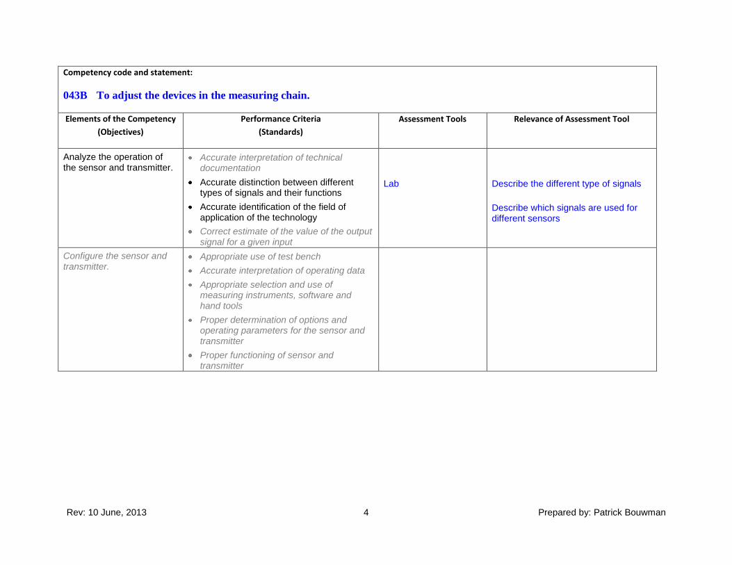
Analyze the operation of the sensor and transmitter.
Accurate interpretation of technical documentation
Accurate distinction between different types of signals and their functions
Accurate identification of the field of application of the technology
Correct estimate of the value of the output signal for a given input
Lab
Describe the different type of signals
Describe which signals are used for different sensors
Configure the sensor and transmitter.
Appropriate use of test bench
Accurate interpretation of operating data
Appropriate selection and use of measuring instruments, software and hand tools
Proper determination of options and operating parameters for the sensor and transmitter
Proper functioning of sensor and transmitter

Rev: 10 June, 2013 5 Prepared by: Patrick Bouwman
Calibrate the sensor and transmitter
Accurate interpretation of operating data
Appropriate selection and use of calibration procedure
Accurate interpretation of calibration curve
Appropriate selection and use of measuring instruments, software and hand tools
Successful simulation of input signals
Proper adjustment of sensor and transmitter
Clear, detailed notes on adjustments made
Observance of occupational health and safety rules
NA Not Relevant
Inspecting the measuring chain.
Accurate interpretation of drawings and technical documentation
Appropriate selection and use of measuring instruments and tools
Appropriate and precise adjustments made to devices in the measuring chain and final controlling elements
Appropriate modifications made to the programs and network configurations
Appropriate use of software
Observance of occupational health and safety rules
NA Not Relevant
Rev: 10 June, 2013 6 Prepared by: Patrick Bouwman
Competency code and statement:
043G To troubleshoot a control system.
Elements of the Competency
(Objectives)
Performance Criteria
(Standards)
Assessment Tools Relevance of Assessment Tool
Gather and analyze information about the malfunction.
Accurate interpretation of service call
Appropriate collaboration with production and maintenance staff
Appropriate use of failure log
Proper determination of emergencies and priorities
Labs
Lab Test/Results
Tests and quizzes
NA
Use of a logical sequence to troubleshoot circuits
Practice working in groups
Explain the results in a log book
Categorize a circuit malfunction
Prepare a test plan
Diagnose the malfunction. Accurate interpretation of drawings, diagrams and technical documentation
Appropriate selection and use of measuring instruments
Appropriate inspection of components
Accurate analysis of the functioning of the process
Appropriate verification of the functioning of power electronics equipment, control unit, devices in the measuring chain, final controlling elements and networks
Appropriate use of troubleshooting guide
Appropriate use of software troubleshooting commands
Proper determination of the nature and cause of the malfunction
Observance of occupational health and safety rules
Labs
Lab Test/Results
Tests and quizzes
Identify the devices and components in the technical documents
Use the appropriate test equipment
Inspect for defective components and devices
Explain the operation of the circuit
Verify the operation of components, devices and instruments
Use of a troubleshooting guide or software tool to diagnose the malfunction
Identify the cause of the malfunction
Properly apply the required safety procedures

Rev: 10 June, 2013 7 Prepared by: Patrick Bouwman
Replace defective components or devices.
Accurate interpretation of drawings, diagrams and technical documentation
Appropriate selection of components or devices
Appropriate selection and use of tools
Proper installation of components or devices
Observance of occupational health and safety rules
Labs
Lab Test/Results
Tests and quizzes
Identify the devices and components in the technical documents
Replace the appropriate defective component or device
Choose the appropriate software to use
Properly apply the required safety procedures
Make the necessary adjustments.
Accurate interpretation of drawings and technical documentation
Appropriate selection and use of measuring instruments and tools
Appropriate and precise adjustments made to devices in the measuring chain and final controlling elements
Appropriate modifications made to the programs and network configurations
Appropriate use of software
Observance of occupational health and safety rules
Labs
Lab Test/Results
Tests and quizzes
Identify the devices and components in the technical documents
Use the appropriate test equipment and tools
Tune the appropriate instruments or devices
Configure the appropriate programs and network configurations
Choose the appropriate software to use
Properly apply the required safety procedures
Restart the control system. Proper application of start-up procedure
Appropriate verification of the functioning of the process
Appropriate instructions given to production staff
Observance of occupational health and safety rules
Labs
Lab Test/Results
Tests and quizzes
Demonstrate the start-up procedure for the control system
Test the functionality of the control system
Follow the appropriate instructions
Properly apply the required safety procedures
Follow up. Proper updating of failure log
Clear formulation of recommendations for preventing a recurrent failure
Production of a service report in conformity with requirements
Labs
Lab Test/Results
Tests and quizzes
Explain the results in a log book
Update the test plan and discuss recommendations
Compose a CSR (customer service report)

Rev: 10 June, 2013 8 Prepared by: Patrick Bouwman
Competency code and statement:
043H To participate in the design of a control project.
Elements of the Competency
(Objectives)
Performance Criteria
(Standards)
Assessment Tools Relevance of Assessment Tool
Analyze the request Identification of the budget
Accurate analysis of company work methods
Proper determination of needs
Proper determination of applicable standards
Adequate planning of project development stages
Labs
Determine the control strategies to be used.
Accurate interpretation of technical documentation
Accurate analysis of the functioning of the process
Accurate analysis of the level of integration of production
Accurate analysis of the characteristics of the control systems
Consideration of safety requirements
Consideration of the competency of existing staff and the required technical support
Consideration of maintenance requirements for the control system
Clear sketches and diagrams
Proper, justified selection of control strategies
Observance of budget constraints

Rev: 10 June, 2013 9 Prepared by: Patrick Bouwman
Determine the material needs.
Accurate interpretation of technical documentation
Appropriate consultation of resource people
Appropriate use of research tools
Appropriate use of test bench
Proper, justified selection of electrical distribution supplies
Proper, justified selection of control units, devices in the measuring chain and final control elements
Observance of budget constraints
Labs
Lab Test/Results
Tests and quizzes
Review technical document requirements
Use appropriate research tools to find technical documents
Use appropriate equipment to test SCC
Develop control programs. Accurate interpretation of technical documentation
Appropriate consultation of resource people
Appropriate use of program development tools
Successful simulation of the functioning of programs
Observance of programming standards
Production of appropriate program documentation
Programs in conformity with control strategies
Labs
Lab Test/Results
Tests and quizzes
Review control program technical documents
Use appropriate control program tools for testing
Develop operator interface. Accurate interpretation of technical documentation
Appropriate consultation of resource people
Accurate analysis of data acquisition, visualization and operation needs
Proper determination of the components of the operator interface
Proper simulation of the functioning of the operator interface

Rev: 10 June, 2013 10 Prepared by: Patrick Bouwman
Finalize the drawings and specifications and have them approved.
Complete detailed list of materials
Proper determination of the stages in the process
Realistic cost estimate
Use of appropriate vocabulary
Clear drawings and specifications
Observance of rules of presentation
Observance of deadlines
Appropriate correction of drawings and specifications
NA Not Relevant

Assignment # 2 Signal Processing 243-234-92 Students Name: __________________________________________________ Please Print Instructions: Mark all answers clearly in the space provided. Make sure all quantities are expressed in their appropriate engineering units Standard resistor values: 2% and 5%
10 16 27 43 68 11 18 30 47 75 12 20 33 51 82 13 22 36 56 91 15 24 39 62 100
1 Patrick Bouwman

1. Consider the following circuit: Rf
20k
U1a
3
21
+
-
R110k
R2100k
Vin
V2-12V Vout
+12V
-12V
Derive the equation of the output Vout as a function of the input Vin, and draw the x-y (Vin - Vout) relationship.
2 Patrick Bouwman
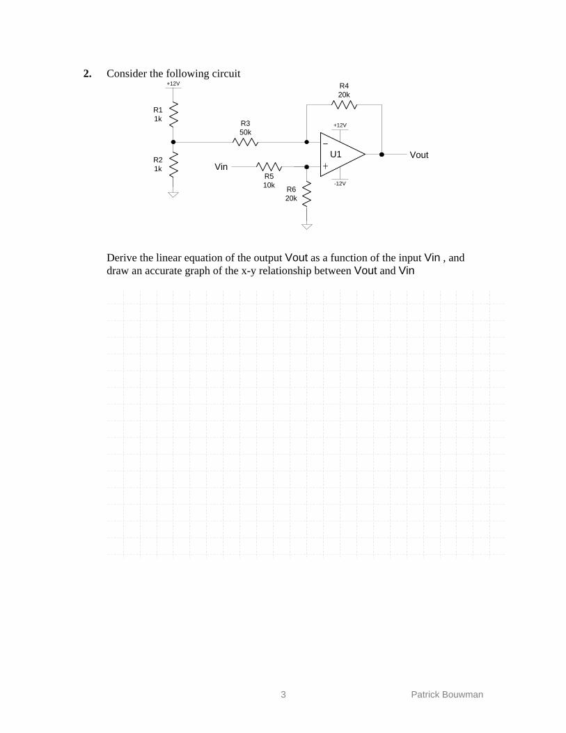
2. Consider the following circuit R420k
R510k
R350k
VinVout
R11k
R21k
+12V
U1+
−
+12V
-12VR620k
Derive the linear equation of the output Vout as a function of the input Vin , and draw an accurate graph of the x-y relationship between Vout and Vin
3 Patrick Bouwman

3. Consider the following circuit.
+
−VinVout
R1100kΩ
C110μF
+
−
R410kΩ
R310kΩ
Express the output voltage Vout as a function of the input voltage Vin. ______________________________________________________ Consider the following input signal Vin for the circuit. In the space provided, draw the output signal Vout
2
1
5 10 15 20
timesec
Vin
5 10 15 20
Vout
timesec
2
1
4
3
4 Patrick Bouwman
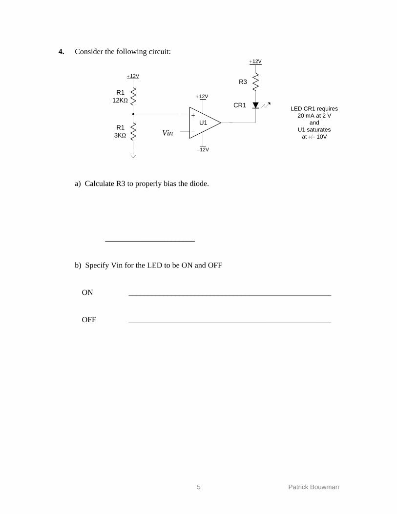
4. Consider the following circuit:
+
−Vin
R112KΩ
+12V
−12V
+12V
R13KΩ
R3
+12V
LED CR1 requires20 mA at 2 V
andU1 saturates
at +/− 10V
CR1
U1
a) Calculate R3 to properly bias the diode. _______________________ b) Specify Vin for the LED to be ON and OFF ON ____________________________________________________ OFF ____________________________________________________
5 Patrick Bouwman
Electrical Engineering Technologies
Industrial Electronics
1 Patrick Bouwman
Signal Processing
Final Exam Part 1 Closed Book
Standard resistor values (5%):
10 16 27 43 68 11 18 30 47 75 12 20 33 51 82 13 22 36 56 91 15 24 39 62 100
Instructions: Mark all answers clearly in the space provided. Make sure all quantities are expressed in their appropriate engineering units Student’s Name: _____________________________________________ Please Print
Electrical Engineering Technologies
Industrial Electronics
2 Patrick Bouwman
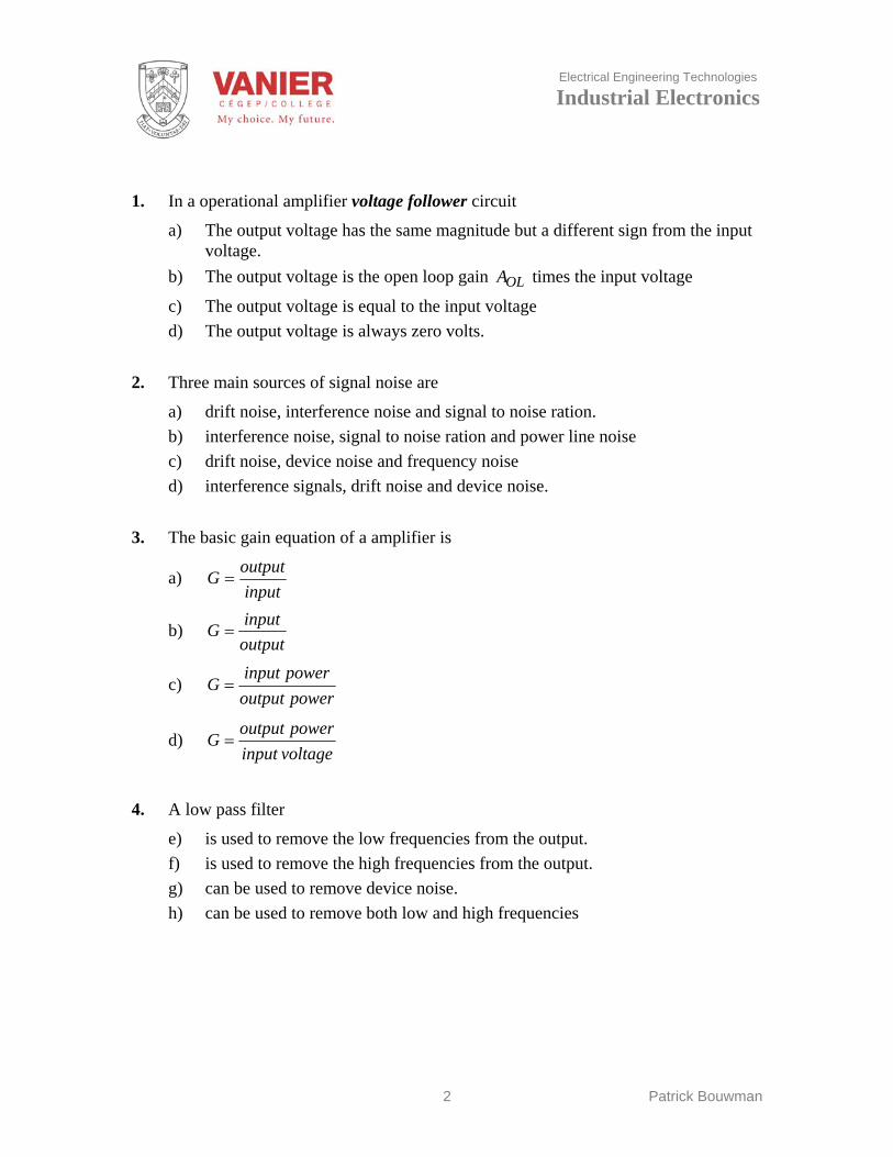
1. In a operational amplifier voltage follower circuit
a) The output voltage has the same magnitude but a different sign from the input voltage.
b) The output voltage is the open loop gain OLA times the input voltage
c) The output voltage is equal to the input voltage d) The output voltage is always zero volts.
2. Three main sources of signal noise are
a) drift noise, interference noise and signal to noise ration. b) interference noise, signal to noise ration and power line noise c) drift noise, device noise and frequency noise d) interference signals, drift noise and device noise.
3. The basic gain equation of a amplifier is
a) inputoutputG =
b) outputinputG =
c) poweroutputpowerinput
G =
d) voltageinputpoweroutput
G =
4. A low pass filter
e) is used to remove the low frequencies from the output. f) is used to remove the high frequencies from the output. g) can be used to remove device noise. h) can be used to remove both low and high frequencies

Electrical Engineering Technologies
Industrial Electronics
3 Patrick Bouwman
5. what method is used to reduce the effect of noise on a comparator is
a) Schmitt trigger b) hysteresis c) both of the above d) none of the above
6. When an op-amp is used as a comparator its output is
a) never saturated b) goes between zero volts and positive saturation. c) goes between zero volts and negative saturation. d) goes between positive and negative saturation.
7. The input resistance of the positive (+) and negative (−) terminals of an op-amp
a) is considered to be zero ohms. b) does not effect its operation. c) is considered to be infinite. d) varies with the input voltage.
8. An amplifier has a power gain of 600. What is the decibel power gain? __________________
9. A two-stage amplifier has gains of 12 dB and −9 dB respectively. What is the total decibel gain? __________________
10. An amplifier has a voltage gain of 27 dB. If the input signal is 12 mV, what is the output voltage? __________________
11. What is the decibel voltage gain of 200 ? __________________
12. An attenuator reduces signal voltage by a factor of 25. What is the loss expressed in decibels ? __________________

Electrical Engineering Technologies
Industrial Electronics
4 Patrick Bouwman
13. Consider the following waveform.
2
1
5 10 15 20
Calculate the average (DC) voltage of the waveform. ______________________________
14. Name the five (5) basic terminals of an operational amplifier.
+
−
15. If the output voltage of a operational amplifier is not in saturation, the voltage between the two input terminals is
a) near zero b) approximatly equal to +V c) equal to Vin d) equal to −V
16. The CMR of an op-amp is equal to its common mode gain over its differential gain
a) true b) false

Electrical Engineering Technologies
Industrial Electronics
5 Patrick Bouwman
17. The voltage follower circuit has a
a) high input impedance b) low output impedance c) unity voltage gain d) all of the above
18. A comparator circuit makes use of the op-amps without using
a) Power supply pins b) negative feedback c) the inverting input d) thenon-inverting input
19. A mathematical operation for finding the area under the curve of a graph is called
a) differentiation b) integration c) curve averaging d) none of the above
20. A practical integrator op-amp circuit has as a feedback component
a) resistor b) capacitor c) inductor d) resistor and capacitor
21. Filter circuits separate signals based on their
a) amplitude b) frequency c) logic level d) wave shape

Electrical Engineering Technologies
Industrial Electronics
6 Patrick Bouwman
22. For a low-pass filter, the 3 dB point is when
a) Vout = 0.1 × Vin b) Vout = 0.5 × Vin c) Vout = 0.707 × Vin d) Vout = 0.909 × Vin
23. Calculate the output voltage ( outV ) for the following amplifier: when Vin = 2 V
+
−Vin
VoutR1100kΩ
R2500kΩ
24. Draw the circuit diagram for an operational amplifier with a gain of +10 using standard 5% resistors values.

Electrical Engineering Technologies
Industrial Electronics
7 Patrick Bouwman rick Bouwman
25. Consider the following circuit. a) What type of filter is this ? __________________________ b) What is the filters cutoff frequency ? __________________________ c) Draw an accurate Bode Plot of the filters’s transfer function.
25. Consider the following circuit. a) What type of filter is this ? __________________________ b) What is the filters cutoff frequency ? __________________________ c) Draw an accurate Bode Plot of the filters’s transfer function.
R122KΩ
C10.047μF
Vin Vout
Electrical Engineering Technologies
Industrial Electronics
8 Patrick Bouwman
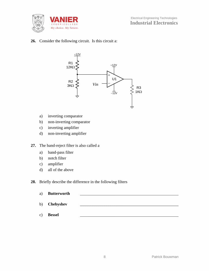
26. Consider the following circuit. Is this circuit a:
+
−Vin
R112KΩ
+12V
−12V
+12V
R23KΩ
U1
R31KΩ
a) inverting comparator b) non-inverting comparator c) inverting amplifier d) non-inverting amplifier
27. The band-reject filter is also called a
a) band-pass filter b) notch filter c) amplifier d) all of the above
28. Briefly describe the difference in the following filters
a) Butterworth ________________________________________________
b) Chebyshev ________________________________________________
c) Bessel ________________________________________________
Electrical Engineering Technologies
Industrial Electronics
9 Patrick Bouwman
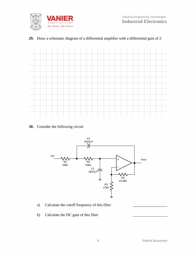
29. Draw a schematic diagram of a differential amplifier with a differential gain of 2
30. Consider the following circuit
+
−R2
33kΩ
C2.0047μF
R133kΩ
C1.0047μF
R327kΩ
R415.8kΩ
VinVout
a) Calculate the cutoff frequency of this filter __________________
b) Calculate the DC gain of this filter __________________

Electrical Engineering Technologies
Industrial Electronics
1 Patrick Bouwman
Signal Processing
Final Exam part 2 Standard resistor values (5%):
10 16 27 43 68 11 18 30 47 75 12 20 33 51 82 13 22 36 56 91 15 24 39 62 100
Instructions: Mark all answers clearly in the space provided. Make sure all quantities are expressed in their appropriate engineering units Student’s Name: _____________________________________________ Please Print

Electrical Engineering Technologies
Industrial Electronics
2 Patrick Bouwman
1. Draw a detailed schematic diagram of an op amp amplifier circuit with a voltage gain of −4.
2. Consider the following waveform.
2
1
5 10 15 20
Calculate the average (DC) voltage of the waveform.
______________________________
Electrical Engineering Technologies
Industrial Electronics
3 Patrick Bouwman
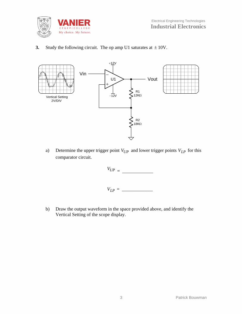
3. Study the following circuit. The op amp U1 saturates at ± 10V.
+
−
+12V
−12V
U1
R112KΩ
R218KΩ
VinVout
Vertical Setting2V/DIV
a) Determine the upper trigger point UPV and lower trigger points LPV for this
comparator circuit.
UPV = _____________
LPV = _____________
b) Draw the output waveform in the space provided above, and identify the Vertical Setting of the scope display.
Electrical Engineering Technologies
Industrial Electronics
4 Patrick Bouwman
4. Given the following circuit R5
20KΩ
Vout
R310KΩ
+
−
+12V
−12V
U1R439KΩ
Vin
+12V
R11.2KΩ
R21.2KΩ
Derive the output voltage Vout as a function of the input voltage Vin.
5. The CMRR of an op-amp is equal to its common mode gain over its differential gain a) true b) false

Electrical Engineering Technologies
Industrial Electronics
5 Patrick Bouwman
6. Draw a schematic diagram for a non-inverting operational amplifier circuit with a gain of 28 dB, using standard 5% resistors values.
Electrical Engineering Technologies
Industrial Electronics
6 Patrick Bouwman
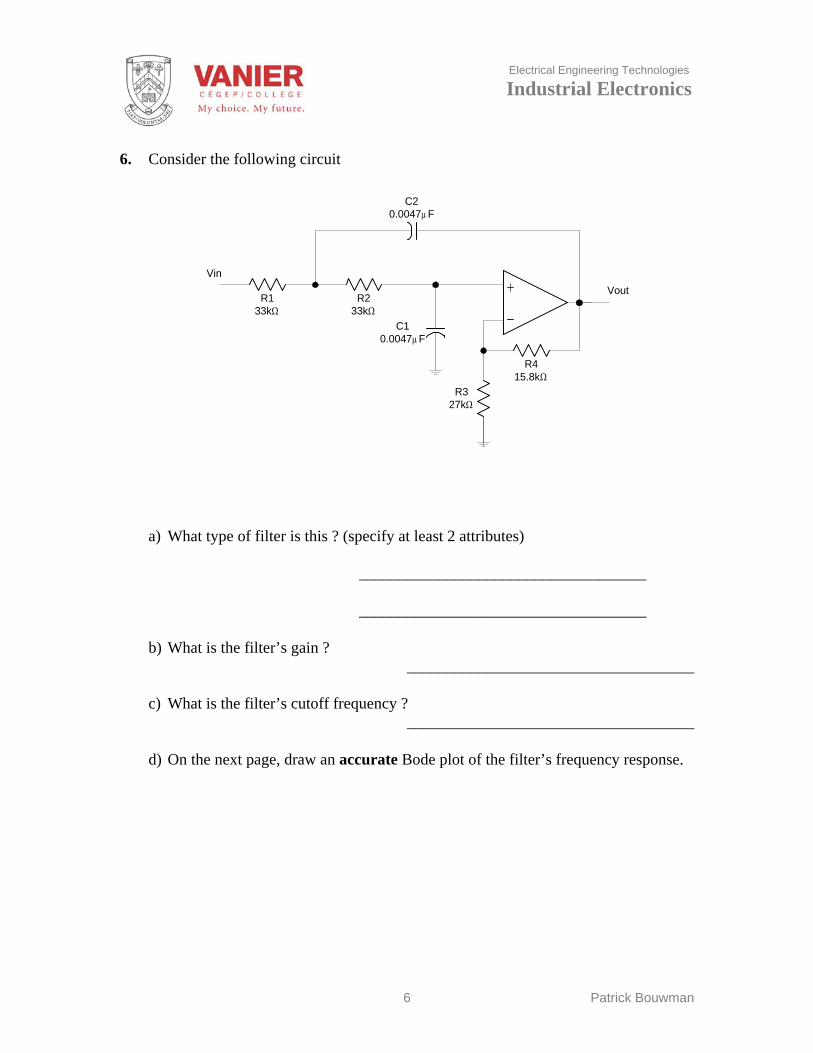
6. Consider the following circuit
+
−R2
33kΩ
C20.0047μF
R133kΩ
C10.0047μF
R327kΩ
R415.8kΩ
VinVout
a) What type of filter is this ? (specify at least 2 attributes) ____________________________________ ____________________________________ b) What is the filter’s gain ? ____________________________________ c) What is the filter’s cutoff frequency ? ____________________________________ d) On the next page, draw an accurate Bode plot of the filter’s frequency response.

Electrical Engineering Technologies
Industrial Electronics
7 Patrick Bouwman
-60
-54
-48
-42
-36
-30
-24
-18
-12
-6
0
6
12
10
dB
100 1,000 10,000 100,000 Frequency (Hz)

Electrical Engineering Technologies
Industrial Electronics
8 Patrick Bouwman
7. Consider the following circuit.
+
−Vin Vout
R2 20kΩ
R120kΩ
R5 20kΩ
R310kΩ +
−
R4 20kΩ
U1a U1b
CR2
CR1
U1 LM747CR1,2 1N914Power +/− 12V
a) What function does this circuit perform ? _______________________________________________________________ b) For what reason is CR1 in the circuit ? _______________________________________________________________ c) draw the output waveform in the space provided.
Vin Vout
Electrical Engineering Technologies
Industrial Electronics
9 Patrick Bouwman
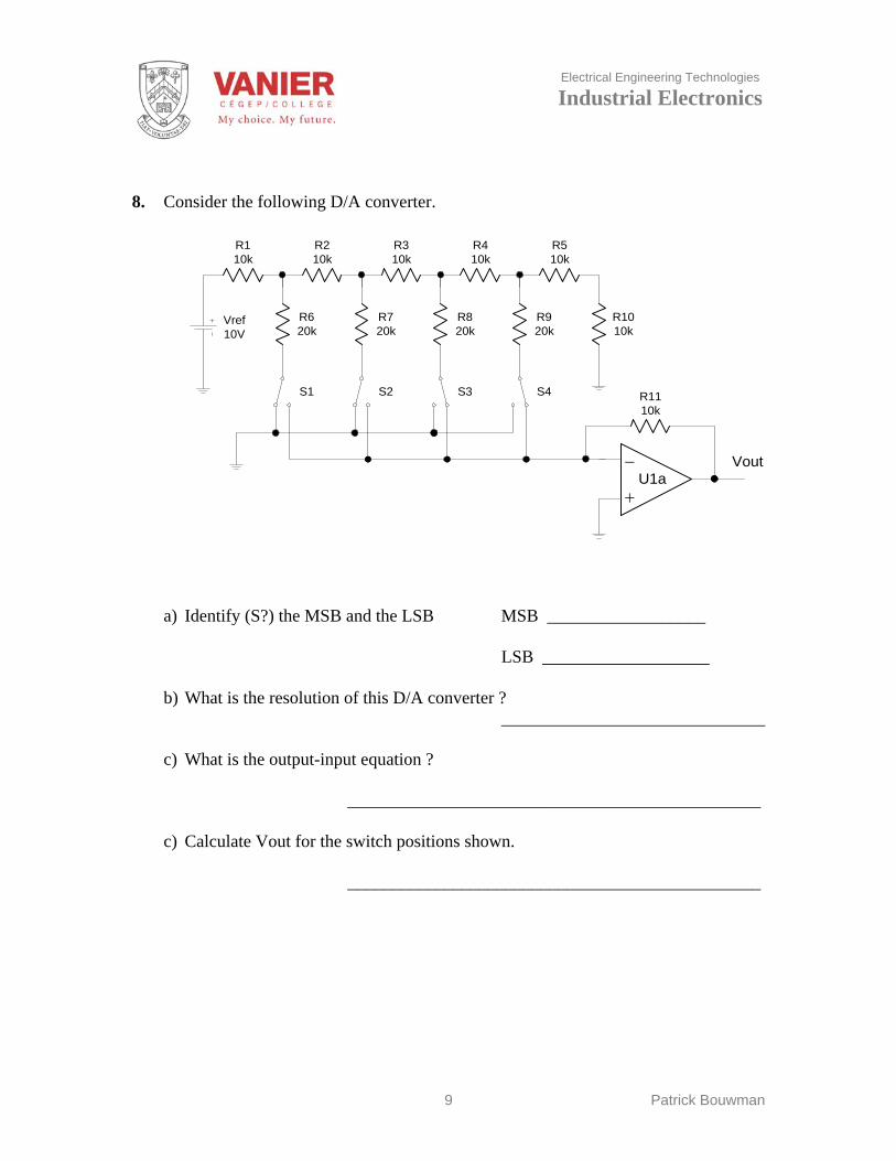
8. Consider the following D/A converter.
R110k
R620k
R210k
R310k
R410k
R510k
R720k
R820k
R920k
R1010k
S1 S2 S3 S4
Vref10V
R1110k
Vout
+
−U1a
a) Identify (S?) the MSB and the LSB MSB __________________ LSB ___________________ b) What is the resolution of this D/A converter ? ______________________________ c) What is the output-input equation ? _______________________________________________ c) Calculate Vout for the switch positions shown. _______________________________________________

Electrical Engineering Technologies
Industrial Electronics
Rev: 7 December, 2012 1 Patrick Bouwman
Lab Test 45 min
7 December, 2012
Closed book
you are allowed to use your Log Book Standard 5% resistor values:
10 16 27 43 68 11 18 30 47 75 12 20 33 51 82 13 22 36 56 91 15 24 39 62 100
Student’s Name: _____________________________________________ Please Print

Electrical Engineering Technologies
Industrial Electronics
Rev: 7 December, 2012 2 Patrick Bouwman
1. Name the five (5) basic terminals of an operational amplifier.
+
−
2. Draw the schematic diagram of a non-inverting op-amp circuit with a gain of 4.
Use standard 5% resistor values, in the range from 1KΩ to 100KΩ
Electrical Engineering Technologies
Industrial Electronics
Rev: 7 December, 2012 3 Patrick Bouwman
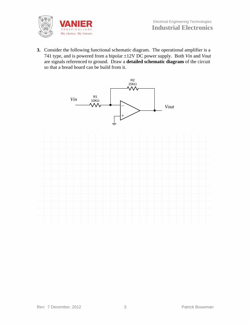
3. Consider the following functional schematic diagram. The operational amplifier is a 741 type, and is powered from a bipolar ±12V DC power supply. Both Vin and Vout are signals referenced to ground. Draw a detailed schematic diagram of the circuit so that a bread board can be build from it.
+
−Vin R1
10KΩ
R215KΩ
Vout

Electrical Engineering Technologies
Industrial Electronics
Rev: 7 December, 2012 4 Patrick Bouwman
4. The input signal for the circuit in question 3 is 2Vp-p no DC offset at 1 KHz, as
shown in the scope display below. In the space below, draw the output signal to scale.
Vin Vout
5. Provide for both oscilloscope displays the horizontal and vertical setting. Vin setting Vout settings Horizontal________________ Horizontal________________ Vertical _________________ Vertical _________________

Electrical Engineering Technologies
Industrial Electronics
1 Patrick Bouwman
Mid Term Lab Test
Open book 60 min.
Instructions: Mark all answers clearly in the space provided. Make sure all quantities are expressed in their appropriate engineering units. Student’s Name: _____________________________________________ Please Print
Electrical Engineering Technologies
Industrial Electronics
2 Patrick Bouwman
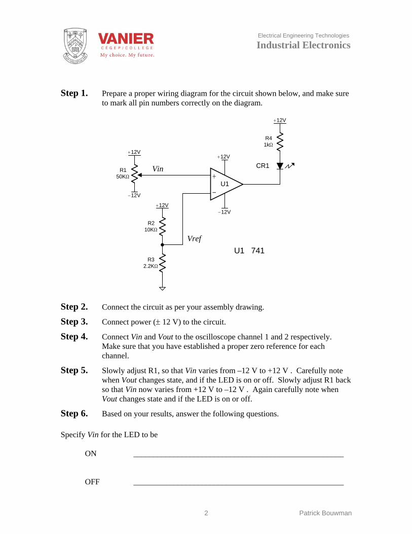
Step 1. Prepare a proper wiring diagram for the circuit shown below, and make sure
to mark all pin numbers correctly on the diagram.
+
−
Vin
R210KΩ
+12V
−12V+12V
R32.2KΩ
R41kΩ
+12V
CR1
U1
R150KΩ
+12V
−12V
VrefU1 741
Step 2. Connect the circuit as per your assembly drawing.
Step 3. Connect power (± 12 V) to the circuit.
Step 4. Connect Vin and Vout to the oscilloscope channel 1 and 2 respectively. Make sure that you have established a proper zero reference for each channel.
Step 5. Slowly adjust R1, so that Vin varies from –12 V to +12 V . Carefully note when Vout changes state, and if the LED is on or off. Slowly adjust R1 back so that Vin now varies from +12 V to –12 V . Again carefully note when Vout changes state and if the LED is on or off.
Step 6. Based on your results, answer the following questions. Specify Vin for the LED to be ON ____________________________________________________ OFF ____________________________________________________

Electrical Engineering Technologies
Industrial Electronics
1 Patrick Bouwman
Quiz # 2
Open book
Standard resistor values: 2% and 5%
10 16 27 43 68 11 18 30 47 75 12 20 33 51 82 13 22 36 56 91 15 24 39 62 100
Instructions: Mark all answers clearly in the space provided. Make sure all quantities are expressed in their appropriate engineering units Student’s Name: _____________________________________________ Please Print
Electrical Engineering Technologies
Industrial Electronics
2 Patrick Bouwman
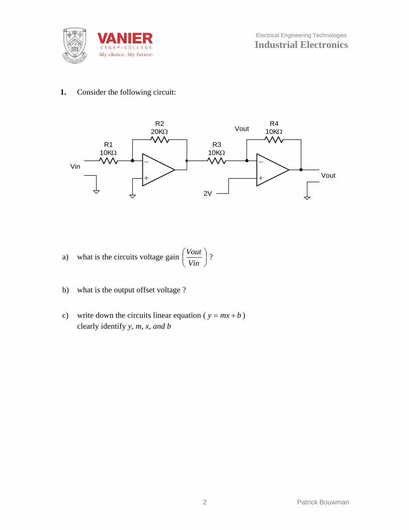
1. Consider the following circuit:
+
−
R110KΩ
VoutR2
20KΩ
Vin
+
−
R310KΩ
R410KΩ
Vout
2V
a) what is the circuits voltage gain ⎟⎠⎞
⎜⎝⎛
VinVout ?
b) what is the output offset voltage ?
c) write down the circuits linear equation ( bmxy += ) clearly identify y, m, x, and b

Electrical Engineering Technologies
Industrial Electronics
3 Patrick Bouwman
2. Consider the following circuit:
Vcc
R12kΩ
R21kΩ
R3510Ω
Q22N3906
U1LM324
24V
outputcurrent
+
−
U1b+
−
U1aQ1
2N3904Vin3V
VA
RL
Ground
For the values shown, calculate the following:
a) the voltage at point VA referenced to ground.
b) the output current when RL is 100Ω
c) what is the largest standard value of RL, for the correct current to flow through RL.

Electrical Engineering Technologies
Industrial Electronics
1 Patrick Bouwman
Quiz # 2
Closed book
Instructions: Mark all answers clearly in the space provided. Make sure all quantities are expressed in their appropriate engineering units Student’s Name: _____________________________________________ Please Print

Electrical Engineering Technologies
Industrial Electronics
2 Patrick Bouwman
1. Briefly describe the difference between a Passive Filter and a Active Filter. ___________________________________________________________________ ___________________________________________________________________ ___________________________________________________________________ ___________________________________________________________________ ___________________________________________________________________ ___________________________________________________________________
2. Filters can be described by their frequency response. Name the four different frequency responses available ? 1. __________________________________________ 2. __________________________________________ 3. __________________________________________ 4. __________________________________________
3. Briefly explain the difference between a first order and a second order Low-Pass Filter.. ___________________________________________________________________ ___________________________________________________________________ ___________________________________________________________________ ___________________________________________________________________
4. Active Low-Pass filters can be classified by type depending on their frequency response at the cutoff point and their pass band characteristics. Name the three different filter types 1. __________________________________________ 2. __________________________________________ 3. __________________________________________
5. A third order active low-pass filter has a roll of how many dB per decade ? _____________________________________

Electrical Engineering Technologies
Industrial Electronics
Rev: 18 November, 2012 1 Patrick Bouwman
Test No. 2 makeup
Instructions: Mark all answers clearly in the space provided. Make sure all quantities are expressed in their appropriate engineering units. Student’s Name: _____________________________________________ Please Print
Electrical Engineering Technologies
Industrial Electronics
Rev: 18 November, 2012 2 Patrick Bouwman
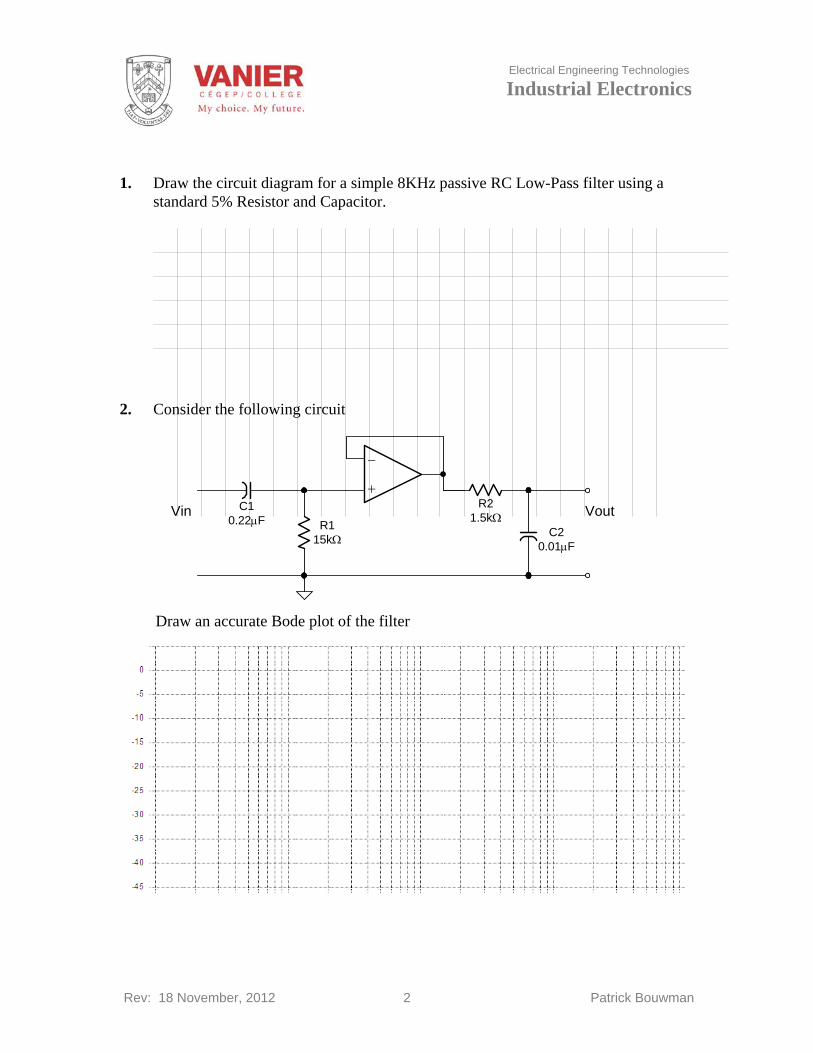
1. Draw the circuit diagram for a simple 8KHz passive RC Low-Pass filter using a standard 5% Resistor and Capacitor.
2. Consider the following circuit
R115kΩ
C10.22μF
R21.5kΩ
C20.01μF
Vin+
−
Vout
Draw an accurate Bode plot of the filter
Electrical Engineering Technologies
Industrial Electronics
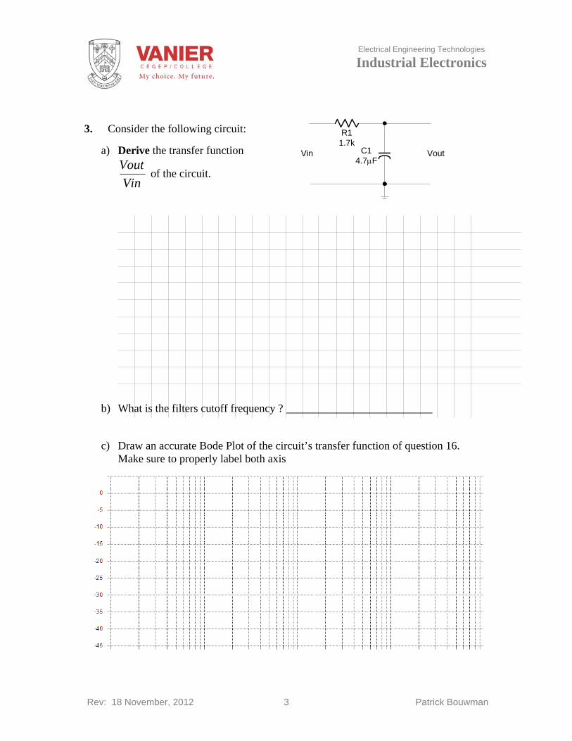
Rev: 18 November, 2012 3 Patrick Bouwman
R11.7k
C14.7μF
Vin Vout
3. Consider the following circuit:
a) Derive the transfer function
VinVout
of the circuit.
b) What is the filters cutoff frequency ? __________________________
c) Draw an accurate Bode Plot of the circuit’s transfer function of question 16. Make sure to properly label both axis

Electrical Engineering Technologies
Industrial Electronics
Rev: 18 November, 2012 4 Patrick Bouwman
4. The general Sallen-Key second order Low-Pass filter is shown below.
CVin
Vout
+
−
R R
C
Ri
Rf
a) Calculate values of Rf and Ri for a Butterworth filter. Use standard 5% resistor values.
Rf = ________________ Ri = ________________
b) Calculate values for R and C for a 3KHz Low-Pass filter. Use standard 5% resistor and capacitor values values.
R = ________________ C = ________________
c) Draw an accurate Bode Plot of the filter. Make sure to properly label both axis

Electrical Engineering Technologies
Industrial Electronics
Rev: 13 November, 2012 1 Patrick Bouwman
Test No. 2
Standard resistor values: 2% and 5%
10 16 27 43 68 11 18 30 47 75 12 20 33 51 82 13 22 36 56 91 15 24 39 62 100
Instructions: Mark all answers clearly in the space provided. Make sure all quantities are expressed in their appropriate engineering units. Student’s Name: _____________________________________________ Please Print

Electrical Engineering Technologies
Industrial Electronics
Rev: 13 November, 2012 2 Patrick Bouwman
1. List the four types of Filters, in terms of frequency response.
a) _______________________
b) _______________________
c) _______________________
d) _______________________
2. Describe the advantage of Active Filters over passive filters.
3. Explain what is meant by the terms “3dB point” and “Corner Frequency”

Electrical Engineering Technologies
Industrial Electronics
Rev: 13 November, 2012 3 Patrick Bouwman
4. A decibel (dB)
a) is equal to ten bels
b) is one tenth of a bel
c) is never used in calculating power gain
d) in never used in calculating voltage gain
5. The basic Gain equation of a Filter is
a) inputoutputgain = f)
output voltageoutputpower gain =
e) outputinputgain = g)
input voltageoutputpower gain =
6. A low pass filter
a) is used to attenuate low frequencies.
b) is used to attenuate high frequencies.
c) is used to amplify low frequencies.
d) Is used to attenuate both low and high frequencies
7. Draw the circuit diagram for a simple 2.2KHz passive RC Low-Pass filter using standard 5% resistor values and a 0.1μF capacitor.

Electrical Engineering Technologies
Industrial Electronics
Rev: 13 November, 2012 4 Patrick Bouwman
8. Consider the following circuit:
R11.7k
C14.7μF
Vin Vout
a) Derive the transfer function
VinVout
of the circuit.
b) What is the filters cutoff frequency ? __________________________
c) Draw an accurate Bode Plot of the circuit’s transfer function of question 16. Make sure to properly label both axis

Electrical Engineering Technologies
Industrial Electronics
Rev: 13 November, 2012 5 Patrick Bouwman
9. The general Sallen-Key second order Low-Pass filter is shown below.
CVin
Vout
+
−
R R
C
Ri
Rf
The Gain(DC) = K will give different filter responses or types based on the follwing table:
K = 1.268 Bessel K = 1.586 Butterworth K = 2.234 Chebyshev
a) Calculate values of Rf and Ri for a Butterworth filter.
Rf = ________________ Ri = ________________
b) Calculate values for R and C for a 2.2KHz Low-Pass filter.
R = ________________ C = ________________
c) Draw an accurate Bode Plot of the filter. Make sure to properly label both axis
Electrical Engineering Technologies
Industrial Electronics
1-1 Patrick Bouwman
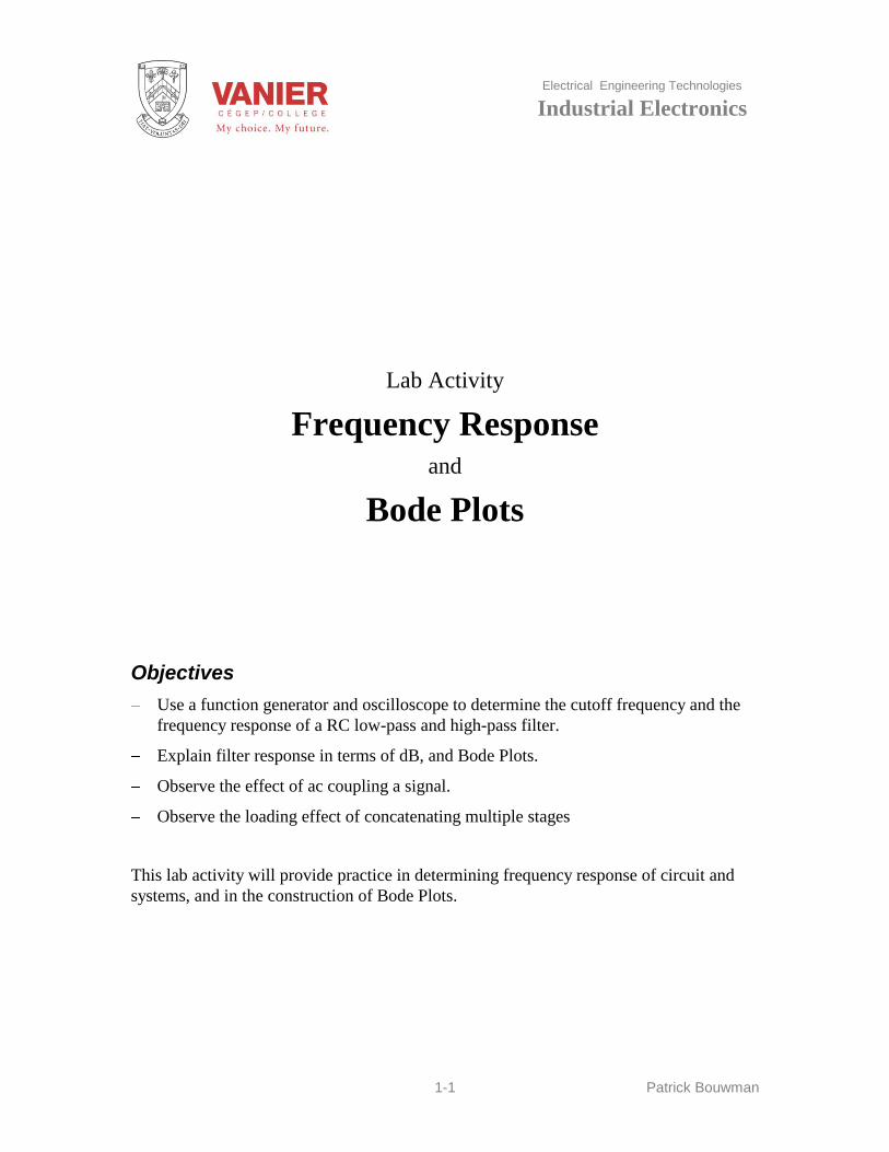
Lab Activity
Frequency Response and
Bode Plots
Objectives
Use a function generator and oscilloscope to determine the cutoff frequency and the
frequency response of a RC low-pass and high-pass filter.
Explain filter response in terms of dB, and Bode Plots.
Observe the effect of ac coupling a signal.
Observe the loading effect of concatenating multiple stages
This lab activity will provide practice in determining frequency response of circuit and
systems, and in the construction of Bode Plots.

Electrical Engineering Technologies
Industrial Electronics
1-2 Patrick Bouwman
Part 1 RC Low Pass filter
In this part of the experiment you will construct and experimentally analyze a simple RC
low-pass filter. You will make voltage measurements at different frequencies, at the
filter’s input and output and convert these measurements to decibels, and then construct a
low-pass Bode Plot.
In DC coupling, the source is directly connected to the system. The DC coupling allows
very slow changing signals to be acquired, but may not produce the desired display due to
offset drift superimposed on top of the desired signal. See step 4
Procedure
1. Assemble the following RC lowpass circuit:
R1
1.5k
C1
.01 F
Vin=1Vp-pFunction
Generator
Vout
CH1 CH2
GND
2. Make sure that your scope is set to DC, and the trigger is set to internal CH1
3. Calculate the theoretical cutoff frequency of the filter and record.
4. Set the function generator to produce a sine wave with an amplitude of 1Vp-p at
1kHz.
5. Slowly vary the function generator’s offset adjustment, and note that the output
follows the input exactly. This is when the signal is dc coupled. The offset
adjustment superimposed on the ac signal can be considered a dc signal at low
frequencies.
6. Before continuing, adjust the dc offset on the function generator back to zero.

Electrical Engineering Technologies
Industrial Electronics
1-3 Patrick Bouwman
7. Slowly adjust the frequency of the function generator until the filter’s output is 3 dB
(0.707 Vp-p) below its input voltage, and record the frequency.
8. Slowly vary the frequency and measure the filter’s input and output voltage at
different frequencies, and plot the filter’s response on a dB vs log frequency scale ie.
Bode Plot.
Note:
When measuring input and output voltages ratios on the oscilloscope, make sure that for
each set of measurements both Vin and Vout are measured at the frequency of interest.
Select your frequencies as required to construct a appropriate Bode plot, noting that the
horizontal axis is logarithmic, and that the bode plot consist primarily of two straight
lines.

Electrical Engineering Technologies
Industrial Electronics
1-4 Patrick Bouwman
Part 2 RC High Pass filter (ac coupling)
In this part of the experiment you will construct and experimentally analyze a simple RC
highpass filter. You will make voltage measurements for different frequencies at the
filters input and output and convert these measurements to decibels to construct a
highpass Bode Plot. You will also observe the effect of ac coupling a signal.
In AC coupling, the source is passed through a capacitor to block the DC component of
the signal, passing the AC portion only. Note that in AC coupling an AC signal must be
present. The DC signal usually presents itself as a slow changing drift superimposed on
the desired AC signal. See step 4
Procedure
1. Assemble the following RC high pass filter circuit.
R1
15k
C1
.22 FVin=1Vp-pFunction
Generator
CH1 CH2
GND
2. Make sure that your scope is set to DC, and the trigger is set to internal CH1
3. Calculate the theoretical cutoff frequency and record.
4. Set the function generator to produce a sine wave with an amplitude of 1Vp-p at
1kHz.
5. Slowly vary the function generator’s offset adjustment, and note that the output resists
to follow the input. Instead the output returns to zero offset. This is when a signal is
ac coupled. The slow varying offset adjustment superimposed on the ac signal is
removed from the higher frequencies.
6. Before continuing, adjust the dc offset to zero, and record your findings of step 4.

Electrical Engineering Technologies
Industrial Electronics
1-5 Patrick Bouwman
7. Slowly adjust the frequency of the function generator until the filters output is 3 dB
below its input, and record
8. Slowly vary the frequency and measure the filter’s input and output voltage at
different frequencies, and plot the filter’s response on a dB vs log frequency scale ie.
Bode Plot.

Electrical Engineering Technologies
Industrial Electronics
1-6 Patrick Bouwman
Part 3 RC Band Pass filter
All systems behave as a simple lowpass filter, with the cutoff frequency above the
frequencies of interest. Most systems that deal with ac signals, also exhibit some type of
ac coupling.
In this part of the experiment you will construct and experimentally analyze a simple RC
bandpass filter. You will make voltage measurements for different frequencies at the
filters input and output and convert these measurements to decibels to construct a
bandpass Bode Plot.
Procedure
1. Assemble the following RC band-pass filter circuit:
R1
15k
C1
.22 F
R2
1.5k
C2
.01 F
Vin=1Vp-pFunction
Generator
CH1 CH2
GND
2. Make sure that your scope is set to DC, and the trigger is set to internal CH1
3. Calculate the theoretical cutoff frequencies and record.
4. Set the function generator to produce a sine wave with an amplitude of 1Vp-p at
1kHz.
5. Adjust the function generator’s dc offset to zero
6. Slowly adjust the frequency of the function generator until the filters output is 3 dB
below its input, and record. Note that this should occur at two specific frequencies.
Explain why.

Electrical Engineering Technologies
Industrial Electronics
1-7 Patrick Bouwman
7. Slowly vary the frequency and measure the filters input and output voltage at different
frequencies, and plot the filters response on a dB vs log frequency scale ie. Bode Plot.
8. Compare your results (Bode plot) with the results obtained in part 1 and 2. Explain
your observations.

Electrical Engineering Technologies
Industrial Electronics
1-8 Patrick Bouwman
Frequency Response and Bode Plots Lab Results
Student’s Name: ___________________________________ Date: ______________
Part 1 RC Low Pass filter
Calculated theoretical cutoff frequency: RC
f2
1 = ______________________
3 dB point input voltage ____________________________
output voltage ____________________________
@ frequency ____________________________
% deviation from theoretical ____________________________

Electrical Engineering Technologies
Industrial Electronics
1-9 Patrick Bouwman
Frequency Response and Bode Plots Lab Results
Student’s Name: ______________________________ Date: ___________________
Part 2 RC High Pass filter (ac coupling)
Calculated theoretical cutoff frequency: RC
f2
1= ______________________
Note offset adjustment superimposed on the ac signal. ______________________
______________________________________________________________________
3 dB point input voltage ____________________________
output voltage ____________________________
@ frequency ____________________________
% deviation from theoretical ____________________________

Electrical Engineering Technologies
Industrial Electronics
1-10 Patrick Bouwman
Frequency Response and Bode Plots Lab Results
Student’s Name: ______________________________ Date: ___________________
Part 3 RC Band Pass filter
Calculated theoretical cutoff frequencies: Low Pass ______________________
High Pass ______________________
3 dB point
Low Pass input and output voltage ____________________________
@ frequencies ____________________________
% deviation from theoretical ____________________________
3 dB point
High Pass input and output voltage ____________________________
@ frequencies ____________________________
% deviation from theoretical ____________________________
Electrical Engineering Technologies
Industrial Electronics
1 Patrick Bouwman
Applications
of
Operational Amplifier
Circuits
Objectives
Identify operational amplifier part numbers
Breadboard simple operational circuits
Voltage Follower
Inverting amplifier
Non-Inverting amplifier
Test breadboarded circuits
These applications will reinforce what we have learned about operational amplifiers, by
building and verifying actual circuit operation.

Electrical Engineering Technologies
Industrial Electronics
2 Patrick Bouwman
The Operational Amplifier Part Number
Most integrated circuit (IC) op-amps are identified by there part numbers, similar to
digital IC’s.
The part number can be divided into four elements.
1. Type (eg. 741)
2. Manufacturer (eg. Analog devices)
3. Specification (eg. temperature range)
4. Mechanical Packaging (eg. DIP)
The letter prefix usually consists of two or three letters that identify the manufacturer
Manufacturers AD Analog Devices
CA RCA
LM National Semiconductors
MC Motorola
NE/SE Signetics
TL Texas Instruments
A Fairchild
Specifications see data sheet
Temperature range C Commercial 0 to 70oC
I Industrial -25 to 85oC
M Military -55 to 125oC
Mechanical N, P Plastic dual-inline
Packaging J Ceramic dual-inline
D Plastic dual-inline for surface mount
H TO-99
For example Packaging N
AD741CN
temperature range C
Manufacturer AD Type 741
Electrical Engineering Technologies
Industrial Electronics
3 Patrick Bouwman
Bread-boarding linear (opamps) IC circuits
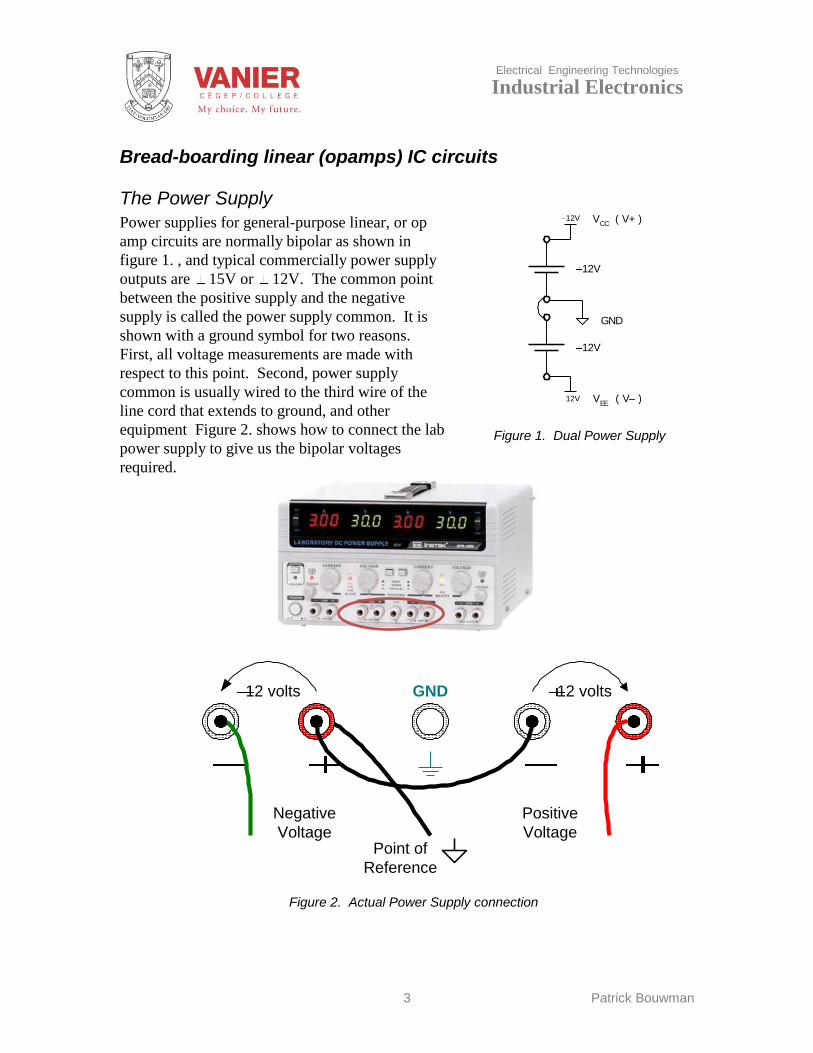
The Power Supply
Power supplies for general-purpose linear, or op
amp circuits are normally bipolar as shown in
figure 1. , and typical commercially power supply
outputs are 15V or 12V. The common point
between the positive supply and the negative
supply is called the power supply common. It is
shown with a ground symbol for two reasons.
First, all voltage measurements are made with
respect to this point. Second, power supply
common is usually wired to the third wire of the
line cord that extends to ground, and other
equipment Figure 2. shows how to connect the lab
power supply to give us the bipolar voltages
required.
12V
12V
12V
12V
GND
VCC
( V+ )
VEE
( V )
Figure 1. Dual Power Supply
Positive
Voltage
Negative
Voltage
GND12 volts 12 volts
Point of
Reference
Figure 2. Actual Power Supply connection

Electrical Engineering Technologies
Industrial Electronics
4 Patrick Bouwman
Some IC op-amps are specified with a single supply (eg. LM324), these units can still
function with dual power supply. Again the op-amp only sees the potential difference of
its positive supply referenced to its negative supply. The signal with these units are also
referenced to the supply center, or can be referenced to the op-amps negative terminal.

Electrical Engineering Technologies
Industrial Electronics
5 Patrick Bouwman
Breadboarding suggestions
Breadboarding is as much an art as a skill, but with a little effort and some common sense
rules much frustration can be avoided, and successful circuits can be produced. The
following ten rules summarize good practice.
1. Prepare a detailed schematic diagram and wiring diagram of the circuit to be
breadboarded. This include checking for the correct pin numbers.
2. Document all connections and changes as you proceed step by step.
3. Do all wiring with power off. It is very important to remember that when changes are
made to a circuit, the power must be disconnected first, before any components are
changed or moved. Only after all changes have been made should power be turned on
or reconnected.
4. Keep wiring and component leads short and flat.
5. Use multiple wires and tie points to make complex wire routings.
6. Wire the power supply and ground first, using the bus bars of the breadboard.
(do not use the bus for signals)
7. Connect signal voltages only after the power is connected to the circuit. (see 9)
8. Take all measurement with respect to ground.
9. Disconnect the input signal before the dc power is removed.
Driving the input pins above or below the power supply may damage the IC (see 7)
10. Connect a 0.1 F capacitor between the power supply pins of the IC and ground if
unwanted oscillation occurs at the output.
When possible section the circuit into functional blocks, build and check each block, then
proceed to interconnect the blocks. (do not forget step 2)
For more information, read the notes on Troubleshooting Op-Amps.

Electrical Engineering Technologies
Industrial Electronics
6 Patrick Bouwman
Part 1 Voltage Follower
In this part you will assemble and test a voltage follower or unity gain noninverting
amplifier. This amplifier has no voltage
gain or loss, and the output signal is in
phase with the input signal. Also, the input
impedance of this amplifier is extremely
high and its output impedance is extremely
low.
The transfer function is given as:
V
V
out
in
1
Procedure
1. Identify the part number of the operational amplifier provided, and using the
specification sheet available on the network (partslib) identify the proper pin numbers
to each terminal.
2. Draw a detailed schematic diagram (including test requirements) before assembling
the circuit. Drawing an assembly diagram will also help in your construction
3. Assemble the circuit per your diagrams. Connect the 10 k load resistor at the output
4. Apply 12 V to the circuits (first measure the power supply voltages before
connecting to your circuit.
5. Using your Digital multimeter measure the DC voltages at the non-inverting input,
inverting input, and output and record. All measurements are referenced to ground.
6. Connect the function generator to the input of the voltage follower, and set the
function generator (using the oscilloscope) to supply the circuit with an input signal of
1 kHz, 1 Vp-p sine wave. Make sure the signal is zero referenced - no DC offset.
7. Using the oscilloscope, measure the peak-to-peak output voltage, and record. Use
both channels if possible, and compare the phase relationship between input and
output and record.
8. Decrease you power supply to 6 V.
Increase the amplitude of the input signal and note that the output voltage follows the
input, until the output is at maximum voltage swing (just before clipping when the
amplifier goes into saturation) and record.
9. Remove the signal source and power, before disassembling/assembling the next
circuit.
Document all your results in your log book.
VinVout
RL
10k
Figure 3. Voltage Follower

Electrical Engineering Technologies
Industrial Electronics
7 Patrick Bouwman
Part 2 Inverting amplifier
In this part you will assemble and test an
inverting voltage amplifier, with a gain of
10. The input impedance of this amplifier
unlike the follower is equal to the input
resistance of the circuits (R1). Its output
impedance is still extremely low.
The transfer function is given as:
V
V
out
in
R2
R1
Procedure
Using the same procedure as in part 1, test
the circuit with an input signal of
1 kHz, 1 Vp-p.
Also perform the following tests:
Adjust the function generator’s offset voltage, and note the output voltage follows the
input voltage with a gain of 10, but inverted (the negative sign). The output signal is
180O out of phase with respect to the input signal, or the output is inverted.
Measure the non-inverting input of the opamp. Does your measurement support the
concept of virtual ground ? Explain your answer.
Modify the circuit so that the voltage gain is reduced to 1.
Document all your results in your log book.
Vin
Vout
R2
15k
R1
1.5kRL
10k
Figure 4. Inverting Amplifier

Electrical Engineering Technologies
Industrial Electronics
8 Patrick Bouwman
Part 3 Non-Inverting amplifier
In this part you will design assemble and
test a non-inverting voltage amplifier,
with a gain of 11. The input impedance
of this amplifier, like the follower, is
extremely high and its output impedance
is extremely low.
The transfer function is given as:
V
V
out
in
1R2
R1
Procedure
Using the same procedure as in part 1, test the circuit with an input signal of
1 kHz, 1 Vp-p.
Also perform the following tests:
Adjust the function generator’s offset, but not its voltage, and note the output voltage
follows the input voltage with a gain of 11. The output signal is in phase with respect to
the input signal, or the output is not inverted.
Modify the circuit so that the voltage gain is reduced to 2.
Document all your results in your log book.
VinVout
R1
1.5k
R2
15k
RL
10k
Figure 5. Non-Inverting Amplifier

Electrical Engineering Technologies
Industrial Electronics
Rev: September, 2012 1 Patrick Bouwman
Applications
of
Operational Amplifiers
Signal Conditioning Circuits
SCC
Objectives
To study the linear equation bmxy , and linear circuits.
Breadboard a Signal Conditioning circuit.
Test the breadboard circuit.
See Applications of Operational Amplifier Circuits Part A for details on identifying
operational amplifiers and breadbording.
These applications will reinforce what we have learned about operational amplifiers, by
building and verifying actual circuit operation.

Electrical Engineering Technologies
Industrial Electronics
Rev: September, 2012 2 Patrick Bouwman
Introduction
Non Inverting Signal Conditioning Circuit
The following linear circuit, is
basically a non inverting amplifier with
an input of V1. Instead of R1 being
connected to ground it is connected to
a second voltage V2.
The output of this circuit is:
VoutR
RV
R
RV1
4
31
4
32
Which is again of the form:
bmxy
Note that the slope m is analogous to
the voltage gain of V1, or
GainR R
Rm
4 3
3, and the y-axis intercept b correspond to a dc offset of
OffsetR
RV b
4
32 when V2 is constant.
V2 Vout
R4
V1
R3
RL

Electrical Engineering Technologies
Industrial Electronics
Rev: September, 2012 3 Patrick Bouwman
For a noninverting gain of 3, we make
mR R
R3
4 3
3
20k 10k
10k and
a dc offset of 3 Vdc, we make
(1.5V)10k
20k2
3
43 V
R
Rb
The graph on the right shows the final
result.
Vout V3 1 3
-10
-8
-6
-4
-2
0
2
4
6
8
10
-10 -8 -6 -4 -2 0 2 4 6 8 10
Input V1
Vout
Electrical Engineering Technologies
Industrial Electronics
Rev: September, 2012 4 Patrick Bouwman
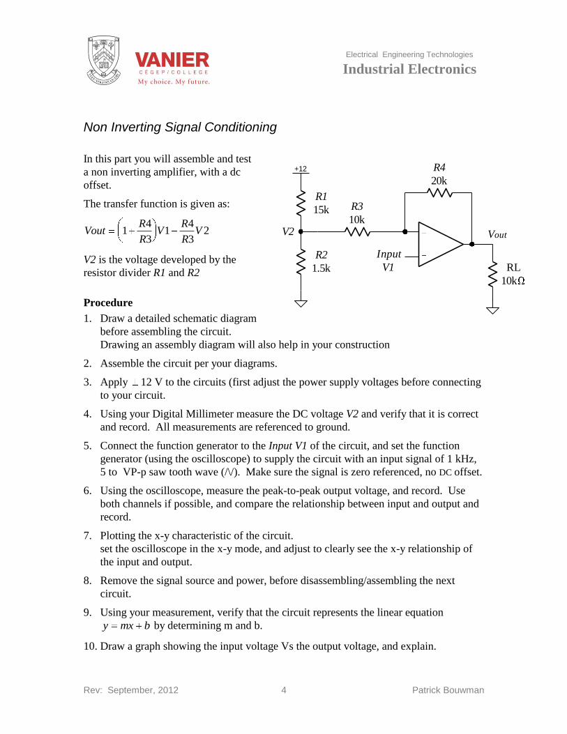
Non Inverting Signal Conditioning
In this part you will assemble and test
a non inverting amplifier, with a dc
offset.
The transfer function is given as:
VoutR
RV
R
RV1
4
31
4
32
V2 is the voltage developed by the
resistor divider R1 and R2
Procedure
1. Draw a detailed schematic diagram
before assembling the circuit.
Drawing an assembly diagram will also help in your construction
2. Assemble the circuit per your diagrams.
3. Apply 12 V to the circuits (first adjust the power supply voltages before connecting
to your circuit.
4. Using your Digital Millimeter measure the DC voltage V2 and verify that it is correct
and record. All measurements are referenced to ground.
5. Connect the function generator to the Input V1 of the circuit, and set the function
generator (using the oscilloscope) to supply the circuit with an input signal of 1 kHz,
5 to VP-p saw tooth wave (/\/). Make sure the signal is zero referenced, no DC offset.
6. Using the oscilloscope, measure the peak-to-peak output voltage, and record. Use
both channels if possible, and compare the relationship between input and output and
record.
7. Plotting the x-y characteristic of the circuit.
set the oscilloscope in the x-y mode, and adjust to clearly see the x-y relationship of
the input and output.
8. Remove the signal source and power, before disassembling/assembling the next
circuit.
9. Using your measurement, verify that the circuit represents the linear equation
y mx b by determining m and b.
10. Draw a graph showing the input voltage Vs the output voltage, and explain.
V2 Vout
R4
20k
Input
V1
R3
10k
R1
15k
R2
1.5k
+12
RL
10k

Electrical Engineering Technologies
Industrial Electronics
Rev: September, 2012 5 Patrick Bouwman
Lab Results
Student’s Name: ___________________________________ Date: ______________
Note the horizontal
and vertical gain
settings of your scope,
and identify the zero
reference for both the
x and y coordinates.
Document all your results in your log book

Electrical Engineering Technologies
Industrial Electronics
Rev: Oct., 2012 1 Patrick Bouwman
The
4 to 20mA
Current Source
Circuit
Objectives
To build a 4 to 20 mA current source circuit.
Breadboard and Test the circuit.
To determine the relationship between input and output.
See Applications of Operational Amplifier Circuits Part A for details on identifying
operational amplifiers and breadboarding.
Electrical Engineering Technologies
Industrial Electronics
Rev: Oct., 2012 2 Patrick Bouwman
Part 1
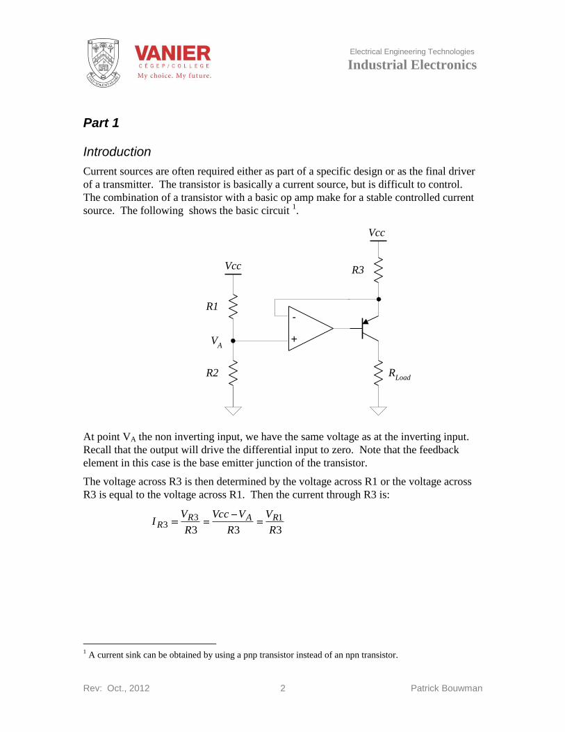
Introduction
Current sources are often required either as part of a specific design or as the final driver
of a transmitter. The transistor is basically a current source, but is difficult to control.
The combination of a transistor with a basic op amp make for a stable controlled current
source. The following shows the basic circuit 1.
+
-
Vcc
VA
Vcc
R1
R2
R3
RLoad
At point VA the non inverting input, we have the same voltage as at the inverting input.
Recall that the output will drive the differential input to zero. Note that the feedback
element in this case is the base emitter junction of the transistor.
The voltage across R3 is then determined by the voltage across R1 or the voltage across
R3 is equal to the voltage across R1. Then the current through R3 is:
333
133
R
V
R
VVcc
R
VI RAR
R
1 A current sink can be obtained by using a pnp transistor instead of an npn transistor.

Electrical Engineering Technologies
Industrial Electronics
Rev: Oct., 2012 3 Patrick Bouwman
Now the collector current equals the emitter current less the base current which is very
small if the beta ( ) of the transistor is large.
Then 3R
VVccI A
Load
The problem with this circuit is that the output current is
proportional to the voltage drop below Vcc, not referenced to
ground.
Recall:
BCE III
BC II
and
100
then I IE C

Electrical Engineering Technologies
Industrial Electronics
Rev: Oct., 2012 4 Patrick Bouwman
4 to 20mA current source
In this part you will assemble and test a voltage to current source circuit. This circuit has
as the input a voltage, and the output is a current through a load resistor.
Before the Lab
Analyze the following circuit, and specify components so that the load current can vary
from 4 to 20mA, while R3 stays constant. R1 and R2 can vary (use a decade box).
Note that the circuit is powered from a single +24V power source, making it compatible
with industry standard equipment.
+
-
Vcc
VA
Vcc
R3
510
RLoad
Q1
2N3906U1
LM324
Vcc
24V
ILoad
mA
Procedure
1. Breadboard the circuit, and verify your calculations.
Initially make RLoad = 0 (short circuit).
2. Tabulate the output current ILoad vs the voltage at point VA.
3. Determine the resistance range of the load (RLoad) for which the circuit will function
within specification (4 to 20mA).

Electrical Engineering Technologies
Industrial Electronics
Rev: Oct., 2012 5 Patrick Bouwman
Current Source 4 to 20mA
Lab Results Student’s Name: ______________________________ Date:__________
Show your calculations here
VA
volts
Iload
mA
Rload
Max
4
6
8
10
12
14
16
18
20

Electrical Engineering Technologies
Industrial Electronics
Rev: Oct., 2012 6 Patrick Bouwman
Part 2
Introduction
The following is in reference to figure 1.
The actual current source consists of operational amplifier U1b, pnp transistor Q2, and
current limiting resistor R3. Resistor R3 is selected to provide sufficient current over a
relative small voltage span. For a standard resistor value of 510 , we have the
following:
at 4mA Vm 04251043 .VR and 96.2104.224AV
at 20mA Vm 2.10510203RV
and 80.132.1024AV
The resistor must not be so small so that the voltage range is too small, and the
operational amplifier needs to function too close to its power supply rail.
This means that the voltage across the load can be as high as 13.8V, less any voltage
required across the emitter-collector junction of transistor Q2 (less than 2V).
The circuit consisting of operational amplifier U1a, npn transistor Q1, and resistors R1
and R2; form a 1-5V to 21.96-13.80V inverting linear conditioning circuit.
The gain of the circuit should be 04.2
51
80.1396.21
In your lab report, explain how this circuit works.
Before the Lab
Analyze the circuit, and prepare a detailed assembly/wiring drawing of your breadboard.
Check the pin numbers against the specification sheet.
Note that the circuit is powered from a single +24V power source, making it compatible
with industry standard equipment.
After the lab
Prepare a detailed lab report based on this lab.

Electrical Engineering Technologies
Industrial Electronics
Rev: Oct., 2012 7 Patrick Bouwman
In your lab report, provide a detailed circuit description of the circuit, and discuss how a
circuit like this can be modified with approriate trim pots (potentiometers) so that it can
be accurately calibrated.
Provide all tabulated results of the output current ILoad vs the input voltage (1-5V).
Prepare a detailed graph based upon your measurements of the input output relationship,
and compare to its theoretical linear equation.

Electrical Engineering Technologies
Industrial Electronics
Rev: Oct., 2012 8 Patrick Bouwman
1-5V input to 4-20mA current source
In this part you will assemble and test the 1-5V input to 4-20mA current output circuit.
See schematic diagram below. This circuit is powered from a single 24V dc power
supply, and the input is a voltage source of 1 to 5V.
Procedure
1. Breadboard the circuit, and verify that your circuit works.
Breadboard and test each part before continuing and connecting them together
Initially make RLoad = 0 (short circuit).
2. Tabulate the output current ILoad vs the input voltage (1-5V).
3. Prepare a detailed graph of the input output relationship.
Vcc
R1
2k
R2
1k
R3
510
Q2
2N3906
U1
LM324
24V
output
4-20mA
+
-
U1b+
-
U1a
Q1
2N3904Vin
input
1-5V
VA
Figure 1. Schematic Diagram
Electrical Engineering Technologies
Industrial Electronics
Rev: October, 2012 1 Patrick Bouwman
Lab Activity
Second Order
Active Low-Pass Filter
Objectives
In this lab activity each student will assemble and test a second order active low-pass
filter.
Use a function generator and oscilloscope to determine the cutoff frequency and the
frequency response of the second order low-pass filters.
Calculate the components required to build one of the following Filter types:
Bessel
Butterworth
Chebyshev
From the data obtained, construct a detailed and accurate Bode Plot, and compare
your results to the theoretical values.

Electrical Engineering Technologies
Industrial Electronics
Rev: October, 2012 2 Patrick Bouwman
Introduction
The following circuit is one of the most popular topologies for a second order low-pass
filter.
C2Vin
Vout
R1 R2
C1
R3
R4
Different filter cutoff frequencies can be obtained by changing the values of R1, R2, C1,
and C2.
If R1 = R2 = R, and C1 = C2 = C, the filter’s cut-off frequency (3dB point) can be
calculated by the simple equation:
CR
fo2
1
Different filter characteristics can be realized by changing the negative feedback gain of
filter (R3 and R4).
If we set
KRKR )1(4
And KRR3 then we can consider K to be the gain (DC) of the filter, since
Gain(DC) = 3
41
R
R=
K
K
R
R)1K(1 = K.
Different values of K will give different filter responses or types as shown in the
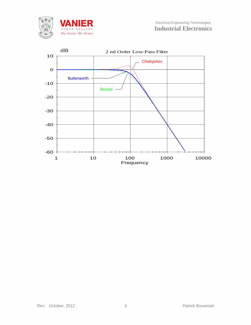
following table.

Electrical Engineering Technologies
Industrial Electronics
Rev: October, 2012 3 Patrick Bouwman
K = 1 0Rf (short), and Ri (open)
K = 1.268 Bessel
K = 1.586 Butterworth
K = 2.234 Chebyshev
The damping factor which normally determines the filter response characteristics is
related to K as:
K32
This means that different filter types using this topology will have different DC gains.
The 3dB point is then measured as 3dB below the filters DC gain.
The filters roll-off slope is 40 dB/dec.
The following Bode Plot shows typical second order low-Pass filter with a cutoff
frequency of 100Hz, and a dc gain of 1
The three different filter types that will be studied are,
Butterworth
Provides a very flat response in the pass band. The phase response is not linear, and will
cause overshoot when a pulse is applied to the filter.
Chebyshev (also spelled Tschebysheff or Tchebysheff)
Characterized by a rapid roll-off, but at the expense of a pass band ripple. The phase
response is even more non linear, and will cause overshoot and oscillation when a pulse is
applied to the filter.
Bessel
The Bessel response exhibits a linear phase characteristic, making it ideal for pulse
waveforms since it produces almost no overshoot. This is at the expense of a poor roll-off
in the stop band.
The following graph shows the three different responses, with a normalized gain of 1.
Electrical Engineering Technologies
Industrial Electronics
Rev: October, 2012 4 Patrick Bouwman
-60
-50
-40
-30
-20
-10
0
10
1 10 100 1000 10000 Frequency
2 nd Order Low-Pass FilterdB
Butterworth
Bessel
Chebyshev

Electrical Engineering Technologies
Industrial Electronics
Rev: October, 2012 5 Patrick Bouwman
Preliminary
Draw a complete schematic diagram of the filter with a gain of 1
( 0Rf , and Ri not connected).
C2
0.1 F
Vin
Vout
R1
2.2K
R2
2.2K
C1
0.1 F
2
3
2U1
Part No.REF +12 -12
LM741U1 7 4
+12
-12
+12V
-12
Part A Butterworth Low-Pass filter
In this part of the experiment you will construct and experimentally analyze the following
active lowpass filter. You will make voltage measurements for different frequencies at
the filter’s input and output and convert these measurements to decibels to construct a
detailed Bode Plot.
Electrical Engineering Technologies
Industrial Electronics
Rev: October, 2012 6 Patrick Bouwman
R2
2.2k
C2
.1 F
R1
2.2k
C1
.1 F
Ri
Rf
Vin
Vout
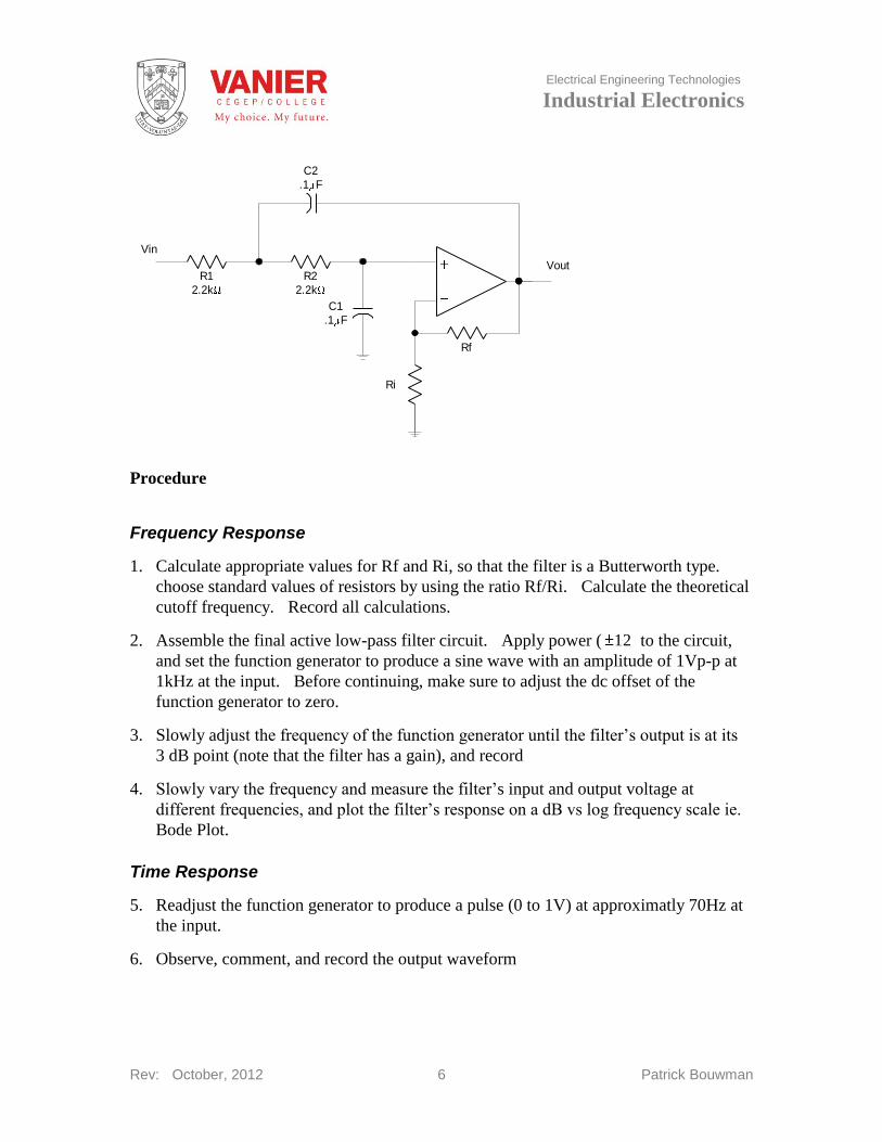
Procedure
Frequency Response
1. Calculate appropriate values for Rf and Ri, so that the filter is a Butterworth type.
choose standard values of resistors by using the ratio Rf/Ri. Calculate the theoretical
cutoff frequency. Record all calculations.
2. Assemble the final active low-pass filter circuit. Apply power ( 12 to the circuit,
and set the function generator to produce a sine wave with an amplitude of 1Vp-p at
1kHz at the input. Before continuing, make sure to adjust the dc offset of the
function generator to zero.
3. Slowly adjust the frequency of the function generator until the filter’s output is at its
3 dB point (note that the filter has a gain), and record
4. Slowly vary the frequency and measure the filter’s input and output voltage at
different frequencies, and plot the filter’s response on a dB vs log frequency scale ie.
Bode Plot.
Time Response
5. Readjust the function generator to produce a pulse (0 to 1V) at approximatly 70Hz at
the input.
6. Observe, comment, and record the output waveform

Electrical Engineering Technologies
Industrial Electronics
Rev: October, 2012 7 Patrick Bouwman
Frequency Response and Bode Plots
Lab Results Student’s Name: ______________________________ Date:__________
Part 1 Butterworth Low-Pass filter
Final Schematic Diagram
Calculated theoretical cutoff frequency: ____________________________
Calculated Rf and Ri ____________________________
Calculated DC gain ____________________________
3 dB point input voltage ____________________________
output voltage ____________________________
@ frequency ____________________________
% deviation from theoretical ____________________________

Electrical Engineering Technologies
Industrial Electronics
Rev: October, 2012 8 Patrick Bouwman
Bode Plot
Time Response
Note the horizontal
and vertical gain
settings of your scope,
and identify the zero
reference for each
signal.

Electrical Engineering Technologies
Industrial Electronics
Rev: October, 2012 9 Patrick Bouwman
Part B
Part 1 Bessel
In this part of the experiment you will construct and experimentally analyze the Bessel
active lowpass filter. (see figure below) You will make voltage measurements for
different frequencies at the filter’s input and output and convert these measurements to
decibels to construct a detailed Bode Plot.
R2
2.2k
C2
.1 F
R1
2.2k
C1
.1 F
Ri
Rf
Vin
Vout
Procedure
Calculate appropriate values for Rf and Ri, so that the filter is a Butterworth type
(K=1.268), use a 2.2k resistor, and the decade box to obtain the proper ratio Rf/Ri,
and calculate the theoretical cutoff frequency and record.
Assemble the final active lowpass filter circuit
Apply power to the circuit, and set the function generator to produce a sine wave with an
amplitude of 1Vp-p at 1kHz at the input.
Before continuing, adjust the dc offset of the function generator to zero.
Slowly adjust the frequency of the function generator until the filter’s output is at its 3
dB point (note that the filter has a gain), and record
Slowly vary the frequency and measure the filter’s input and output voltage at different
frequencies, and plot the filter’s response on a dB vs log frequency scale ie. Bode
Plot.

Electrical Engineering Technologies
Industrial Electronics
Rev: October, 2012 10 Patrick Bouwman
Readjust the function generator to produce a pulse (0 to 1V) at 1kHz at the input.
Observe, comment, and record the output waveform
Part 2 Chebyshev
In this part of the experiment you will construct and experimentally analyze the
Chebyshev active lowpass filter
Repeat part 1 using K=2.234
Prepare a detailed lab report comparing the filter types.

Electrical Engineering Technologies
Industrial Electronics
Rev: 12 August, 2012 1 Patrick Bouwman
Applications
of
Operational Amplifier
Circuits
Comparators
Objectives
To study the use of operational amplifiers in the use of comparator circuits.
Breadboard and test
non-inverting comparator
inverting comparator
the schmitt trigger
characterizing the schmitt trigger using the x-y oscilloscope function.
See Applications of Operational Amplifier Circuits Part A for details on identifying
operational amplifiers and breadboarding.
These applications will reinforce what we have learned about operational amplifiers, by
building and verifying actual circuit operation.

Electrical Engineering Technologies
Industrial Electronics
Rev: 12 August, 2012 2 Patrick Bouwman
Introduction
Consider the following circuit.
Note that the circuit has no
feedback connection, and is
operating in what is refered to as
open loop.
Recall that the op-amp, amplifies
(with a very large gain) the
differential voltage applied to its input terminals, or
)( VVAVout ol
In the circuit shown, since V is connected to ground (zero volts), the equation reduces
to:
VinAVout ol
This means that for Vin > 0, Vout = +Vsat
and Vin < 0, Vout = Vsat
Vin Vout
R1

Electrical Engineering Technologies
Industrial Electronics
Rev: 12 August, 2012 3 Patrick Bouwman
Non-inverting zero crossing detector
Assemble the following circuit
using a 747 type op-amp
connected to 12 volts.
Connect Vin and Vout to the
oscilloscope channel 1 and 2
respectively. Make sure that you
have established a zero reference
for each.
Slowly adjust Vin from 2V to
+2V, and observe the output
voltage.
Inverting zero crossing detector
Modify the circuit as shown
(interchanging the inputs), and
repeat the above experiment.
Compare the input / output characteristics of both circuits.
Vin
VoutR1
10K
12V
12V
50K
12V
12V
Vin
VoutR1
10K
12V
12V
50K
12V
12V

Electrical Engineering Technologies
Industrial Electronics
Rev: 12 August, 2012 4 Patrick Bouwman
The schmitt trigger circuit
Assemble the following circuit
using a 747 type op-amp
connected to 12 volts.
Connect Vin and Vout to the
oscilloscope channel 1 and 2
respectively. Make sure that you
have established a zero reference
for each.
Adjust the function generator to
make Vin a triangular waveform
centered around zero with an
amplitude of 1 volts, and a
frequency of 100 Hz.
Note that Vout does not shange.
Explain why.
Increase Vin to 10 volts and note what happens. Explain why
Measure and record the input and output waveforms of the circuit, and draw the result
accurately in the space provided.
Note the horizontal
and vertical gain
settings of your scope,
and identify the zero
reference for each
signal.
Vin
triangle Vout
R1
10K
12V
12V
R3
10KR2
4.7K

Electrical Engineering Technologies
Industrial Electronics
Rev: 12 August, 2012 5 Patrick Bouwman
Comparator
Lab Results Student’s Name: ______________________________ Date:__________
Plotting the x-y characteristic of the schmitt trigger.
set the oscilloscope in the x-y mode, and adjust to clearly see the hysterasis of the schmitt
trigger
Note the horizontal and vertical gain settings of your scope, and identify the zero
reference for both the x and y coordinates
Electrical Engineering Technologies
Industrial Electronics
Rev: August, 2012 1 Patrick Bouwman
Applications
of
Operational Amplifier
circuits
Integration
Objectives
The purpose of this activity is to demonstrate the response of a integrator to periodic
waveforms.
Breadboard and test a
Integrator
Describe the basic integrator circuits
Use the oscilloscope and function generator to test circuit operation
These applications will reinforce what we have learned about operational amplifiers, by
building and verifying actual circuit operation.
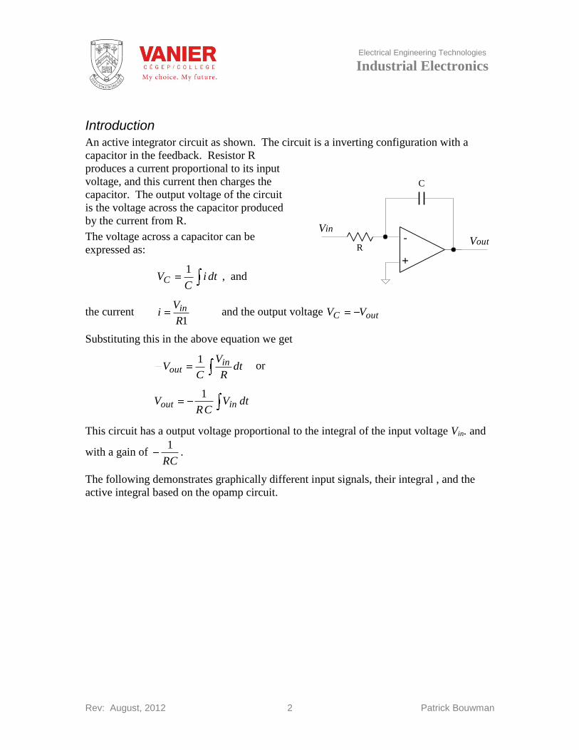
Electrical Engineering Technologies
Industrial Electronics
Rev: August, 2012 2 Patrick Bouwman
Introduction
An active integrator circuit as shown. The circuit is a inverting configuration with a
capacitor in the feedback. Resistor R
produces a current proportional to its input
voltage, and this current then charges the
capacitor. The output voltage of the circuit
is the voltage across the capacitor produced
by the current from R.
The voltage across a capacitor can be
expressed as:
dtiC
VC1
, and
the current 1R
Vi in and the output voltage outC VV
Substituting this in the above equation we get
dtR
V
CV in
out1
or
dtVCR
V inout1
This circuit has a output voltage proportional to the integral of the input voltage Vin. and
with a gain of RC
1.
The following demonstrates graphically different input signals, their integral , and the
active integral based on the opamp circuit.
+
-Vin
VoutR
C

Electrical Engineering Technologies
Industrial Electronics
Rev: August, 2012 3 Patrick Bouwman
t
t
t
t
t t t
t t
t
t
t t
t
t
Vm sin t
True
Integration
-Vm sin t
Op Amp
Integration
Vm sin t
RC
k (constant)
+Vm
+Vm
-Vm
+Vm
-Vm
k tk
k t
RC
T
Ranp
v=k t
k t2
2-- k t2
2 RC
-Vm

Electrical Engineering Technologies
Industrial Electronics
Rev: August, 2012 4 Patrick Bouwman
Procedure
1. Assemble the following circuit The second op-amp is a inverting amplifier with a
unity gain, making the output of the active integrator nonnverting.
Vin
Vout
R1
10k
C1
.022 F
R2
100k
R4
10k
R3
10k
2. Use Channel 1 of your oscilloscope to monitor the input of the circuit and Channel 2
to monitor the output. The input mode select switch for each channel should be set in
the DC position after using the GND position to establish a 0V reference line for the
upper and lower traces. Use the center horizontal line on the screen for the 0 V
reference line for the Channel 1 upper trace and the bottom horizontal line for the
Channel 2 reference line. Set the volts/div control for Channel 1 to 0.5 V/div, and the
volts/div control for Channel 2 to 2 V/div. The time/div control should be set at 0.5
ms/div. Trigger from Channel 1 in the Auto mode.
3. Use your function generator to apply a 0 to l Vpeak, 1 kHz pulsating DC square wave
to the input. Make sure the square wave starts at exactly 0V and rises to +l V for each
pulse. You need to adjust the DC offset control and the amplitude control several
times to produce this square wave. Also, the square wave should have a 50% duty
cycle.
4. Accurately draw the input and output signals of the screen in your log book.
5. Increase the frequency to 4kHz, and describe its effect on the output.
6. Lower the frequency of the pulsating DC until the DC signal displayed on Channel 2
becomes rippled (noticeable triangle waveform). This should be a very low
frequency.
7. Using the integrator circuit, verify and experiment with different signals as shown in
the introduction. Document each waveform, and comment on amplitude, and shape.
8. Answer all the following questions.

Electrical Engineering Technologies
Industrial Electronics
Rev: August, 2012 5 Patrick Bouwman
Integrator
Lab Results Student’s Name: ______________________________ Date:__________
1. Draw the input and output signals of step 4 in the space provided. Identify both the
horizontal and vertical axis.
2. For the circuit assembled, what does the final output voltage represent ?

Electrical Engineering Technologies
Industrial Electronics
Rev: August, 2012 6 Patrick Bouwman
3. What is the voltage amplification for the circuit and how is this determined ?
4. What is the average value of the pulsating DC applied to the input at step 4.

Electrical Engineering Technologies
Industrial Electronics
Rev: August, 2012 7 Patrick Bouwman
Electrical Engineering Technologies
Industrial Electronics
Rev: August, 2012 1 Patrick Bouwman
Waveform
Generation
Objectives
To be able to connect a integrated circuits from information provided by the
manufacturer’s data sheet.
To investigate the effect of ac and dc coupling waveforms.
To mix appropriate sinusoidal waveforms to produce complex waveforms.
Reference Reading
ICL8038 or XR-8038 datasheet

Electrical Engineering Technologies
Industrial Electronics
Rev: August, 2012 2 Patrick Bouwman
Introduction
The ICL8038 integrated circuit, has the capability of generating sinusoidal, triangular, and
square waveforms. It forms the heart of some commercial signal generators and is a
popular device for experimenters. The block diagram shows its simplified function.
Timing
Circuit
(Oscillator)
Sine
Converter
Square
Converter
Sine Wave
Triangle Wave
Square Wave
Timing
Capacitor
Figure 1. Block Diagram
No attempt will be made in this experiment to understand the internal operation of this
integrated circuit. However students are encouraged to study its data sheet (reflib on the
network), to fully understands is function . It is easy to use, however, by following and
understanding the manufacturer's suggested configurations, and application information.
The manufacturer's data specifies various ranges for particular components. The ranges
picked for this experiment fall within the specified ranges, and will produce waveforms
with a 50% duty cycles. The student will observe that some of the waveforms are less
than perfect. The reason for this is that the circuit configuration is a simple one. More
external design is needed to obtain optimum performance from the integrated circuit as
explained in the data sheet. All details are provided in the data sheet, and we will apply
some of these techniques later when required.
The three outputs of this chip each have a DC offset voltage along with the AC waveform
component. This will allow the study of the effect of using a capacitor to couple a signal.
It will be seen that the capacitor will remove the DC level, in the same way that a scope’s
AC coupling does.

Electrical Engineering Technologies
Industrial Electronics
Rev: August, 2012 3 Patrick Bouwman
1
2
3
4
5
6
7
14
13
12
11
10
9
8
DCA1
VCC
FMBI
NC
NC
SA2
VEE
TC
SQO
DB4
SA1
SWO
TWO
DCA2
Figure 2. Pin Out
Before we apply the ICL8038 we will identify each pin, to fully understand its functional
description in relation to its functional diagram. (also see Figure 2.)
Pin Number(s) Symbol Description
1 SA1 Sine Waveform Adjust Input 1. This pin is used together with pin
12 to adjust the harmonic distortion of the sine output.ÁÁÁ
2 SWO Sine Wave Output
3 TWO Triangle Wave Output
4 DCA1 Duty Cycle Adjustment Input 1. Duty cycle can be adjusted using
this pin in combination with pin 5.
5 DCA2 Duty Cycle Adjustment Input 2
6 VCC Positive Power Supply
7 FMBI Frequency Modulation Input. ÁÁÁ
8 FMSI Frequency Sweep Input.
9 SQO Square Wave Output. ÁÁÁ
10 TC Timing Capacitor Input.
11 VEE Negative Power Supply.
12 ÁÁÁÁÁ SA2 Sine Waveform Adjust Input 2.
13 NC No Connect. ÁÁÁ
14 NC No Connect. ÁÁÁ ÁÁÁÁÁÁÁÁÁÁÁÁ

Electrical Engineering Technologies
Industrial Electronics
Rev: August, 2012 4 Patrick Bouwman
Procedure
1. Connect the test circuit as recommended in the manufacturer’s data sheet. Do not
turn on power until all of the circuit is connected.
Sine Wave
Triangle Wave
Square Wave
ICL8038
2
3
4 5 6
1110
DCA1
+10V
VEETC
SQO
SWO
C1
0.1 F
use a decadebox
to vary the
frequency
DCA2
RA
100k
RB
100k
VCC
TWO
10V
RL
10k
Note:
Measure all outputs
referenced to ground
(see notes on dual
power supplies)
7
8
FMBI
FMSI
9
Figure 3. Test Circuit
1. Use the oscilloscope to measure the waveform at each specified output of the
integrated circuit, and record. (frequency, shape, and amplitude; draw an accurate
picture,)
2. Use a DC voltmeter to measure the DC and rms voltage levels of each waveform and
record.
Change C1 repeat steps 1. Determine how the frequency changes as the value of the
capacitor changes, Always turn off the power when making changes to the circuit.

Electrical Engineering Technologies
Industrial Electronics
Rev: August, 2012 5 Patrick Bouwman
3. Add a 0.1 F capacitor in series with the output of pin number 2. Observe the
waveform on the scope with the input set for dc coupling. Measure on both sides of
the capacitor in order to see the effect it has on the output waveform.
4. Modify the circuit as explained in the data sheet so that the frequency can be varied
(modulated) using a potentiometer as explained in the data sheet. Use a 50k
potentiometer and a 100k resistor. Expalin why.
ICL8038
2
3
4 5 6
1110
DCA1
+10V
VEETC
SQO
SWO
C1
0.0047 F
DCA2
RA
100k
RB
100k
VCC
TWO
10V
RL
10k
7
8
FMBI
FMSI
9
RA
50k
RA
100k

Electrical Engineering Technologies
Industrial Electronics
Rev: September, 2012 1 Patrick Bouwman
Lab Activity
Common Mode Rejection
Objectives
This lab activity is designed to measure the common node rejection ratio (CMRR) of
a differential operational amplifier circuit.
Express the CMRR in terms of dB.
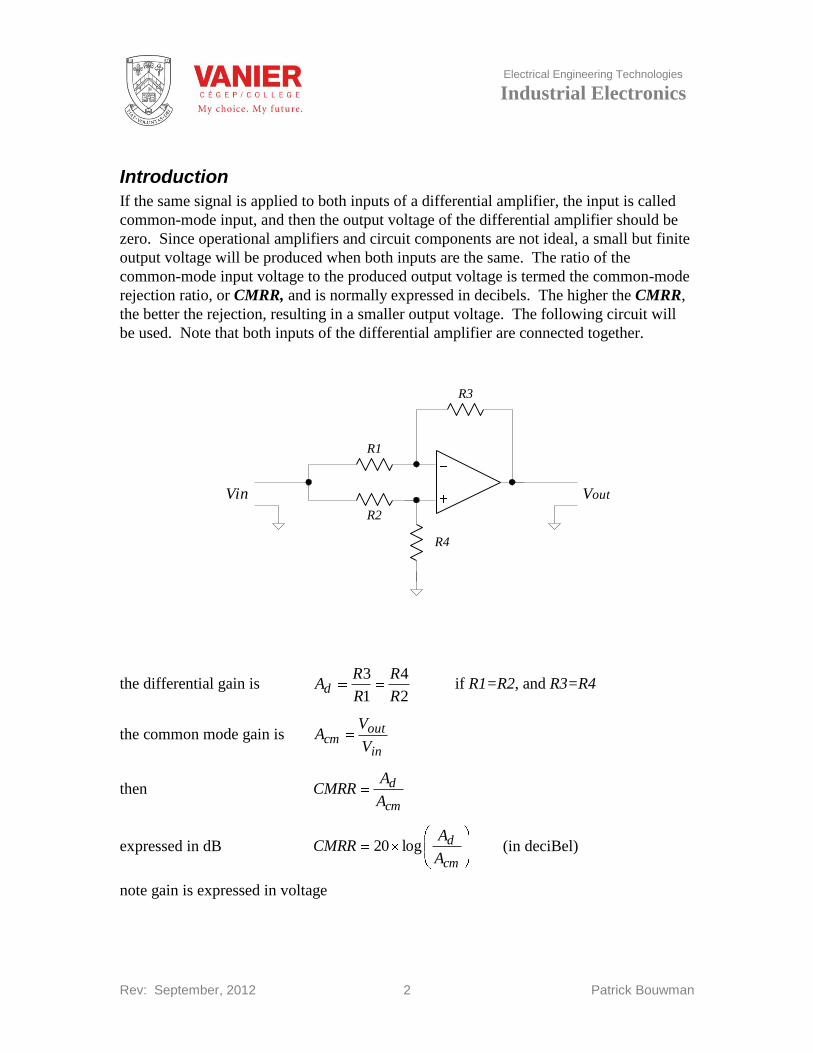
Electrical Engineering Technologies
Industrial Electronics
Rev: September, 2012 2 Patrick Bouwman
Introduction
If the same signal is applied to both inputs of a differential amplifier, the input is called
common-mode input, and then the output voltage of the differential amplifier should be
zero. Since operational amplifiers and circuit components are not ideal, a small but finite
output voltage will be produced when both inputs are the same. The ratio of the
common-mode input voltage to the produced output voltage is termed the common-mode
rejection ratio, or CMRR, and is normally expressed in decibels. The higher the CMRR,
the better the rejection, resulting in a smaller output voltage. The following circuit will
be used. Note that both inputs of the differential amplifier are connected together.
Vout
R3
Vin
R1
R4
R2
the differential gain is 2
4
1
3
R
R
R
RAd if R1=R2, and R3=R4
the common mode gain is in
outcm
V
VA
then cm
d
A
ACMRR
expressed in dB cm
d
A
ACMRR log20 (in deciBel)
note gain is expressed in voltage

Electrical Engineering Technologies
Industrial Electronics
Rev: September, 2012 3 Patrick Bouwman
PROCEDURE
Assemble the following circuit using a 741 type op-amp, making sure all connections are
short and close together.
Vout
R3
154k
Vin
R1
154k
R4
54k
R2
154k
Note: All
resistors are 1%
Apply 12V power to the circuit.
Connect the input to the function generator and adjust to 1.0 Vp-p sine wave (no offset) at
a frequency of 60 Hz using channel 1 of the oscilloscope. Also, concurrently, measure its
RMS voltage using the DMM.
Measure both the RMS and peak-to-peak output voltage using channel 2, and record all
results.
From your measurements, calculate the CMRR of the circuit.
Calculate the CMRR of the 741 operational amplifier based on the actual (measured)
values of the resistors.
Compare your results with those published by the manufacturer of the 741 operational
amplifier.
Repeat your measurements and calculations using a 324 type op-amp.

Electrical Engineering Technologies
Industrial Electronics
Rev: August, 2012 1 Patrick Bouwman
Applications
of
Operational Amplifier
Circuits with Diodes
Objectives
To study the following circuits
half wave rectifier
peak detector
full wave rectifier (absolute value)
signal limiter
Breadboard and test the circuit.
These applications will reinforce what we have learned about operational amplifiers, by
building and verifying actual circuit operation.

Electrical Engineering Technologies
Industrial Electronics
Rev: August, 2012 2 Patrick Bouwman
Introduction
Half wave rectifier
The following circuit is a positive precision half-wave rectifier. This circuit will be able
to rectify signals that are smaller than a diode voltage drop(diode barrier potential). The
operational amplifier enable the diode to behave like an ideal diode.
ac in
dc out
RLNote the distortion
Notice that the output is taken from the input of the inverting amplifier. During the
positive cycle, the amplifier is connected as a voltage follower with the diode forward
biased. During the negative cycle, the amplifier will go into negative saturation, and the
diode will be reverse biased, and the inverting input will remain at zero potential.
Resistor RL makes sure that the diode is forward biased. When the op-amp needs to
return from negative saturation, it will require some time to recover. This causes the
distortion as shown. We will see later how to avoid this
Peak detector
The same circuit, with the addition of a capacitor makes a peak detector.
ac in peak
outputC RL
The capacitor during the positive cycle will charge until the output voltage equals the
input voltage as long as the input voltage is greater than the voltage across the capacitor.
At this point, the op-amp (as a comparator) switches, and the op-amp’s output goes to

Electrical Engineering Technologies
Industrial Electronics
Rev: August, 2012 3 Patrick Bouwman
negative saturation. The diode is now reverse biased, and the capacitor will hold its
charge. If later a larger input voltage occurs, the capacitor will charge to its new peak
voltage.
Signal Limiter
Diodes in the feedback are often used to limit a signal’s amplitude. As long as the input
signal is below approximately 1Vpp ( 0.5V) the signal will be inverted. If the signal
exceeds the diode barrier potential, the signal will be amplitude limited.
input output
R
R

Electrical Engineering Technologies
Industrial Electronics
Rev: August, 2012 4 Patrick Bouwman
Full wave rectifier
The following circuit is a full-wave precision rectifier..
ac indc out
R
R
R
R/2
R
inverting amplifier
(summer)
negative half-wave
rectifier
Looking at the circuit we see that the first part consists of a negative half-wave rectifier,
and the second part is a summer. The summer adds the original signal plus twice the
inverted half-wave rectified signal producing the full wave-rectification as shown.

Electrical Engineering Technologies
Industrial Electronics
Rev: August, 2012 5 Patrick Bouwman
ac in
full-wave
output
half-wave
output
half-wave
output x2
+
X2
X-1
Part 1 Half wave rectifier
Assemble the following circuit.
ac indc out
U1 747/324
CR1 1N914
RL 1k to 10k
Power +/- 12V U1
CR1
RL
Using an appropriate input, verify that the circuit is functional. Document your results in
the space provided.
Electrical Engineering Technologies
Industrial Electronics
Rev: August, 2012 6 Patrick Bouwman
Record the horizontal
and vertical gain
settings of your scope,
and identify the zero
reference for each
signal

Electrical Engineering Technologies
Industrial Electronics
Rev: August, 2012 7 Patrick Bouwman
Part 2 Peak detector
Assemble the following circuit
ac in
peak
outputC1
1 F
U1 747/324
CR1 1N914
RL 1k to 10k
Power +/- 12VU1
CR1
RL
Using an appropriate input, verify that the circuit is functional. Document your results in
the space provided.
Record the horizontal
and vertical gain
settings of your scope,
and identify the zero
reference for each
signal

Electrical Engineering Technologies
Industrial Electronics
Rev: August, 2012 8 Patrick Bouwman
Part 3 Full wave rectifier
Assemble the following circuit
ac indc out
R2
20k
R1
20k
R5
20k
R3
10k
R4
20k
U1a U1b
CR2
CR1
U1 747/324
CR1,2 1N914
Power +/- 12V
Using an appropriate input, verify that the circuit is functional. Document your results in
the space provided.
Record the horizontal
and vertical gain
settings of your scope,
and identify the zero
reference for each
signal

Electrical Engineering Technologies
Industrial Electronics
Rev: August, 2012 9 Patrick Bouwman
Part 4 Signal Limiter
Assemble the following circuit
input
outputR1
10k
U1 747
CR1,2 1N914
Power +/- 12V
U1
CR1
CR2
R2 20k
Using an appropriate input, verify that the circuit is functional. Document your results in
the space provided.
Record the horizontal
and vertical gain
settings of your scope,
and identify the zero
reference for each
signal

Electrical Engineering Technologies
Industrial Electronics
Rev: March, 2011 1 Patrick Bouwman
Sample and Hold
Objectives
The purpose of this activity is to assemble, troubleshoot, and demonstrate the operation of
a Sample and Hold Circuit used in Data Acquisition and Control industry. Specifically:
To analyze the operation of a sample and hold circuit.
To evaluate the relationship between the incoming analog frequency and the sampling
frequency.
To reconstruct an analog waveform from a sampled waveform.
To observe the effect of aliasing distortion and its causes.
This experiments will reinforce what we have learned about Data Acquisition and the
need for a Sample and Hold Circuit.

Electrical Engineering Technologies
Industrial Electronics
Rev: March, 2011 2 Patrick Bouwman
Materials Required
Resistor: 10K
Capacitors: 47nF (2), 100 nF, 10 µF (2)
N-Channel Enhancement MOSFET VN10KM
LM324 Op amp
Oscilloscope
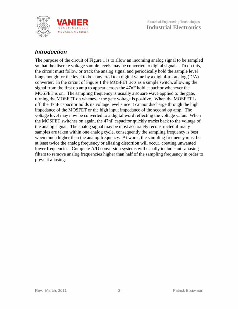
Electrical Engineering Technologies
Industrial Electronics
Rev: March, 2011 3 Patrick Bouwman
Introduction
The purpose of the circuit of Figure 1 is to allow an incoming analog signal to be sampled
so that the discrete voltage sample levels may be converted to digital signals. To do this,
the circuit must follow or track the analog signal and periodically hold the sample level
long enough for the level to be converted to a digital value by a digital-to- analog (D/A)
converter. In the circuit of Figure 1 the MOSFET acts as a simple switch, allowing the
signal from the first op amp to appear across the 47nF hold capacitor whenever the
MOSFET is on. The sampling frequency is usually a square wave applied to the gate,
turning the MOSFET on whenever the gate voltage is positive. When the MOSFET is
off, the 47nF capacitor holds its voltage level since it cannot discharge through the high
impedance of the MOSFET or the high input impedance of the second op amp. The
voltage level may now be converted to a digital word reflecting the voltage value. When
the MOSFET switches on again, the 47nF capacitor quickly tracks back to the voltage of
the analog signal. The analog signal may be most accurately reconstructed if many
samples are taken within one analog cycle, consequently the sampling frequency is best
when much higher than the analog frequency. At worst, the sampling frequency must be
at least twice the analog frequency or aliasing distortion will occur, creating unwanted
lower frequencies. Complete A/D conversion systems will usually include anti-aliasing
filters to remove analog frequencies higher than half of the sampling frequency in order to
prevent aliasing.

Electrical Engineering Technologies
Industrial Electronics
Rev: March, 2011 4 Patrick Bouwman
Procedure
Observing Sample and Hold Operation
Step 1. Connect the circuit of Figure 1 using 10µF noise-filtering capacitors across
the 12 V power supplies for the op amps. Observe capacitor polarities to
prevent an explosion hazard.
Figure 1. Sample and Hold Circuit
Step 2. Connect a 100 Hz sine wave generator as the analog input. Set its amplitude
to 1.4 Vp-p. Set the frequency as close as you can to the 100Hz value.
Step 3. Connect a 1.00KHz square wave generator as the sampling input. Set its
amplitude to 2.5 Vp-p. Set the frequency as close as you can to the 1.00KHz
value.
From time to time in this experiment it may be necessary to momentarily short-circuit the
100nF capacitor so that the circuit can begin operation. If the sampling voltage is initially
set too high and then decreased to the required setting, the circuit will sometimes fail to
operate. If the sampling voltage is initially set too low and then increased to the required
setting, the circuit will always operate correctly. A brief short across the 100nF capacitor
will restore operation.
Step 4. With the oscilloscope triggered on the analog signal, observe the output
waveform. You will probably see the small hold samples moving
continuously through the 100 Hz waveform. This is normal because no
matter how carefully you set the two frequencies, they will never be exactly a
10:1 ratio since they are separate unrelated generators, and each will drift to
some extent.
Step 5. Adjust one of the generators very carefully and try to stop the motion of the
sample levels, or at least slow the movement as much as possible.

Electrical Engineering Technologies
Industrial Electronics
Rev: March, 2011 5 Patrick Bouwman
Step 6. Count the number of sample points within one cycle of the 100Hz analog
signal. Record.
Step 7. Adjust the analog frequency to 200 Hz and repeat steps 5 and 6. Repeat this
for the frequencies setting of ??
Observing Signal Reconstruction
Step 8. Add a RC low pass filter to the output of the circuit as shown in Figure 2.
Figure 2. Reconstructed Output
Step 9. Set the analog signal back to 100Hz and observe the waveform across the
47nF capacitor of the RC low-pass filter. Record.
This would be similar to how a reconstructed waveform would appear if it had been
digitized and then converted back to analog with a digital-to-analog (D/A) converter.
Step 10. Set the analog signal to 200Hz and observe the waveform across the 47nF
capacitor of the RC filter. Record.
Step 11. Set the analog signal to 500Hz and observe the waveform across the 47nF
capacitor of the RC low-pass filter. Record.
Observing Aliasing
Step 12. Remove the RC low pass filter from the circuit and set the analog frequency
to about 980Hz. Set the scope sweep rate to 10 ms/div and observe the
appearance of the alias frequency. record your observations in your log
book.
Step 13. Slowly adjust the analog signal from 950Hz to 1050Hz and observe the
various alias frequencies.

Electrical Engineering Technologies
Industrial Electronics
Rev: March, 2011 6 Patrick Bouwman
Observing High Sampling Rates
Step 14. Reset the analog signal to 100Hz and increase the sampling frequency to
10KHz. Observe that the output is now being sampled many times per cycle,
more than you can easily count. This would represent a more typical
relationship between the analog frequency and the sampling frequency for
some but certainly not all applications.
Questions
1. When the VN10KM is on, the specification for its R DS(on) is 7.5 . What is the
expected charging time constant for the hold capacitor? What is the time required to
reach full charge (5t)?
2. To prevent aliasing distortion when the sampling frequency is 1.0KHz, what is the
maximum allowable input analog frequency?
3. If the analog input frequency to the sample and hold circuit is 500Hz and its period is
therefore 2.00ms, determine what percentage of this period time would be required
for the 47nF capacitor to reach its full charge.
4. The time to reach full charge should be less than 0.5 % of the period of the input
analog frequency. Is this circuit within an acceptable range?
5. What would happen if the hold capacitor were increased to 4.70µF?

Electrical Engineering Technologies
Industrial Electronics
Rev: August, 2012 1 Patrick Bouwman
Application
Analog to Digital
A/D
Conversion
Objectives
This lab activity will study the use of a typical analog to digital converter, and its input
output characteristics by breadboarding and testing the circuit.
To build the A/D converter circuits
Study its input output characteristics

Electrical Engineering Technologies
Industrial Electronics
Rev: August, 2012 2 Patrick Bouwman
Successive Approximation Analog to Digital (A/D) Conversion
The Successive Approximation Register (SAR) Principle
The block diagram for a basic 4-bit SAR A/D is shown in Figure 1. Initially, the register
is set to 0 (00002). The control logic then modifies the contents of the SAR, bit by bit.
Each new binary number generated is fed to the DAC, where the analog voltage is
produced (Vout) and sent to the comparator. When the conversion process is complete,
the digital output reflects the input analog voltage at Vin.
+
-Clock
SAR
DAC
Vincomparitor
(8)
D
(4)
C
(2)
B
(1)
A
DCBA
Vout
MSB
LSB
Figure 1. Block Diagram
To examine the concept a bit further. First, a clock pulse is sent to the control logic. It in
turn, outputs a signal that sets the SAR’s most significant bit (MSB) to 1. The register
then contains the value 10002. The DAC then generates an analog output voltage, Vout,
equivalent to the number 10002, and sends it to the inverting input of the comparator. If
this voltage is greater than Vin, the comparator outputs a LOW, causing the MSB to reset
to 0. If the voltage is less than Vin, the comparator outputs a HIGH. and the 1 is retained
in the MSB location. This process now repeats with the next most significant bit, until all
bits have been checked. After all the bits from the SAR have been placed, the conversion
cycle is complete. The digital output then reflects the analog voltage input, within the
resolution of the converter.
The following example will illustrate the circuit’s operation, by analyzing how a 4-bit
A/D converter, converts a 1.5V analog input to the equivalent binary number 01012.
Assume that the A/D converter has a range from 0 to 5. This means it has a resolution of
333.15
5
12
54
V/bit. This means Vout = 2.67V for the D(8) bit (MSB),
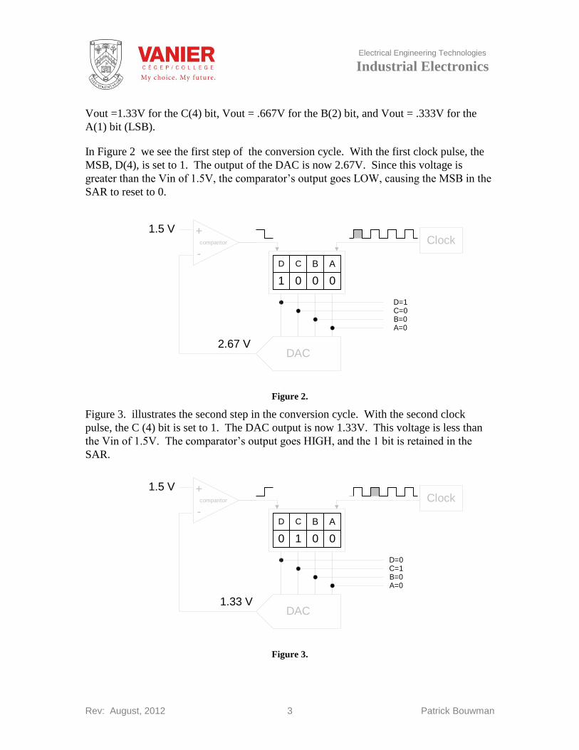
Electrical Engineering Technologies
Industrial Electronics
Rev: August, 2012 3 Patrick Bouwman
Vout =1.33V for the C(4) bit, Vout = .667V for the B(2) bit, and Vout = .333V for the
A(1) bit (LSB).
In Figure 2 we see the first step of the conversion cycle. With the first clock pulse, the
MSB, D(4), is set to 1. The output of the DAC is now 2.67V. Since this voltage is
greater than the Vin of 1.5V, the comparator’s output goes LOW, causing the MSB in the
SAR to reset to 0.
+
-
Clock
DAC
1.5 Vcomparitor
D=1C=0B=0A=0
2.67 V
ABCD
0001
Figure 2.
Figure 3. illustrates the second step in the conversion cycle. With the second clock
pulse, the C (4) bit is set to 1. The DAC output is now 1.33V. This voltage is less than
the Vin of 1.5V. The comparator’s output goes HIGH, and the 1 bit is retained in the
SAR.
+
-
Clock
DAC
1.5 Vcomparitor
D=0C=1B=0A=0
1.33 V
ABCD
0010
Figure 3.

Electrical Engineering Technologies
Industrial Electronics
Rev: August, 2012 4 Patrick Bouwman
Figure 4. shows the third step in the conversion cycle. With the third clock pulse, the B
(2) bit is set to 1. Note, though, that the DAC now outputs 2.00V, not .667V as you
might first expect. This is because the C and B bits are both set to 1, and giving a Vout of
1.33 +.67=2.00V. Since this voltage is greater than 1.5 V, the comparator’s output goes
LOW, and the B bit is reset to 0.
+
-
Clock
DAC
1.5 Vcomparitor
D=0C=1B=1A=0
2.00 V
ABCD
0110
Figure 4.
Figure 5. illustrates the fourth, and last, step in the conversion cycle. With the fourth
clock pulse, the A (1) bit is set to 1 and the DAC output is now 1.67 V (the A and C bits
are set to 1).
+
-
Clock
DAC
1.5 Vcomparitor
D=0C=1B=0A=1
1.67 V
ABCD
1010
Figure 5.
At this point the conversion cycle is complete, since all 4 bits have been tried. The binary
output of 01012 is the closest value to the 1.5 V input analog voltage. A new conversion
cycle can now begin.

Electrical Engineering Technologies
Industrial Electronics
Rev: August, 2012 5 Patrick Bouwman
Note that during the conversion only four clock pulses were required. This illustrates an
important advantage of the successive approximation A/D. It has a fixed conversion time
that is independent of the input analog voltage, unlike other types of A/D converters. An
N-bit SAR A/D will require N clock pulses to perform a conversion, regardless of the
level of the input analog voltage. The following timing diagram (Figure 6.) summarizes
the sequence.
Clock
comparitor output
D
C
B
A
Reset
Reset
0
1
0
1
DAC Vout
2.67
1.33
2.001.67
Time
Final Value
Figure 6. Timing Diagram

Electrical Engineering Technologies
Industrial Electronics
Rev: August, 2012 6 Patrick Bouwman
The ADC0804 A/D converter (the real thing)
Complete 8-bit successive-approximation A/D converters are available as a single IC
(Integrated Circuit), usually in 18 or 20 pins DIP (Dual In-line Package). They contain an
on-chip clock generator, the successive approximation register (SAR), an 8-bit DAC, all
control logic, and three-state outputs to facilitate computer bus interfacing. Figure 7.
shows the pin configuration for a typical 8-bit A/D converter chip, the ADCO804. The
ADC0804 is a member of a family of A/D converters. For a detailed description and
application information refer to its data sheet, ADC0801.pdf in the parts library. CS
1
2
3
4
5
6
7
8
9
10
20
19
18
17
16
15
14
13
12
11
CLK IN
Vin(+)
Vin(-)
A GND
Vref/2
D GND
Vcc
CLK R
DB0
DB1
BD2
DB3
DB4
DB5
DB7
DB8
RD
WR
INTR
CS
Figure 7. ADC0804 pin out
Before we apply the A/D we will identify each pin, to fully understand its functional
description in relation to its functional diagram. Note that many of the pins are identified
with computer terminology, since most ADC arc used to interface with microprocessors.
Pin Number(s) Symbol Description
1 CS Active LOW chip select. For the ADCO8O4 to operate, it must
be asserted LOW.
2 RD Active LOW read pin. When LOW, the tri-state outputs are
active and the digital output DB7 - DB0 can be read.
3 WR
An active LOW write pin. When it goes LOW, the A/D
conversion process begins.
4 CLK IN Clock input pin. A clock signal is available from pin 19, or any
TTL level square wave signal source will do.

Electrical Engineering Technologies
Industrial Electronics
Rev: August, 2012 7 Patrick Bouwman
5 INT Active LOW interrupt, or halt pin. When LOW it signals that
the conversion process is complete. If connected to WR the
conversion process will immediately begin again.
6 and 7 Vin(+) and Vin( ) Differential input. Usually, the Vin(+) input is used and the
Vin(-) is grounded.
8 A GND Analog ground connection for the analog input voltage.
9 Vref/2 Controls the voltage to which the analog input voltage is
referenced. If left unconnected, the reference is Vcc.
10 D GND Digital ground for the device and digital outputs.
11 - 18 DB7 - DB0 These are the tri-state buffered digital outputs.
19 CLK R This is the output from the internal clock. Its frequency is
determined by an external resistor and capacitor.
20 Vcc This is the supply voltage, typically +5 V, though it can go as
high as 6.5 V.
Application
In Figure 8. a test/demonstration circuit for the ADC0804 is detailed. This circuit will
convert an analog input voltage of from 0 to 5 V (potentiometer R2 is acting as a voltage
divider) and produce an equivalent digital output with full 8-bit resolution, in a
conversion time of approximately 13 ms.
The external resistor capacitor R1, C1 will setup a clock frequency of
Hz600p150k101.1
1
1.1
1
RC
The connection from INTR to WR will cause the A/D to start a new conversion each time
the INTR (end of conversion line goes low. S1 is used to make sure that an initial first
conversion takes place.
The CS is grounded to enable the A/D converter chip.
The RP is grounded to enable the D0 - D7 outputs.
The analog input voltage is positive 0 - 5V referenced to ground, so it is connected to
Vin(+) , and Vin( ) is connected to ground.
The outputs D0 - D7 are connected to light emitting diodes through a current limiting
resistor of 330 .

Electrical Engineering Technologies
Industrial Electronics
Rev: August, 2012 8 Patrick Bouwman
Since the analog input voltage is directly proportional to the digital output, the following
ratio applies.
256
Dout
Vref
Vin or 256
VrefDout
Vin digital output in base 10
Our resolution is 6.19255
5
12
58
mV/bit.
R1
10k
C1
150pF
1
2
3
4
5
6
7
8
9
10
20
19
18
17
16
15
14
13
12
11
Vcc
+5 V
R10
R3 - R10 330
D1 - D8 LEDs
R3
D8
+5 V
R2
100k
Vin
Momentary
short to
start
conversion
S1
D1
CLK IN
Vin(+)
Vin(-)
A GND
Vref/2
D GND
Vcc
CLK R
DB0
DB1
BD2
DB3
DB4
DB5
DB6
DB7
RD
WR
INTR
ADC0804
U1
CS
Figure 8. Connection for continuous conversion