sakhrat khizroev - center for nanoscale information devices next generation memory devices florida...
TRANSCRIPT
Sakhrat Khizroev - Center for Nanoscale Information Devices
Next Generation Memory Devices
Florida International University Miami, Florida, U.S.A.
Center for Nanoscale Magnetic Devices
Sakhrat Khizroev
Sakhrat Khizroev - Center for Nanoscale Information DevicesPage 2
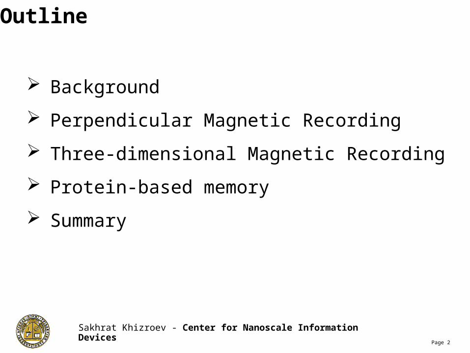
Outline
Background
Perpendicular Magnetic Recording
Three-dimensional Magnetic Recording
Protein-based memory
Summary
Sakhrat Khizroev - Center for Nanoscale Information DevicesPage 3
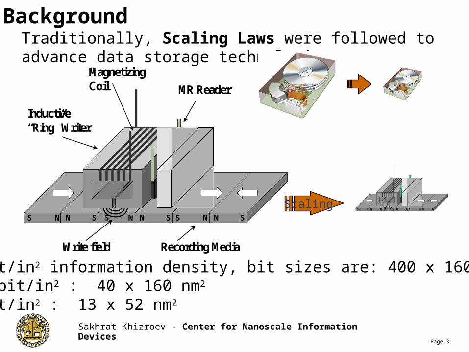
BackgroundTraditionally, Scaling Laws were followed to advance data storage technologies
S N N S N SS N S NN S
Inductive“Ring” Writer
MR Reader
MagnetizingCoil
Write field Recording Media
S N N S N SS N S NN SScaling
At 1 Gbit/in2 information density, bit sizes are: 400 x 1600 nm2
At 100 Gbit/in2 : 40 x 160 nm2
At 1 Tbit/in2 : 13 x 52 nm2
Sakhrat Khizroev - Center for Nanoscale Information DevicesPage 4
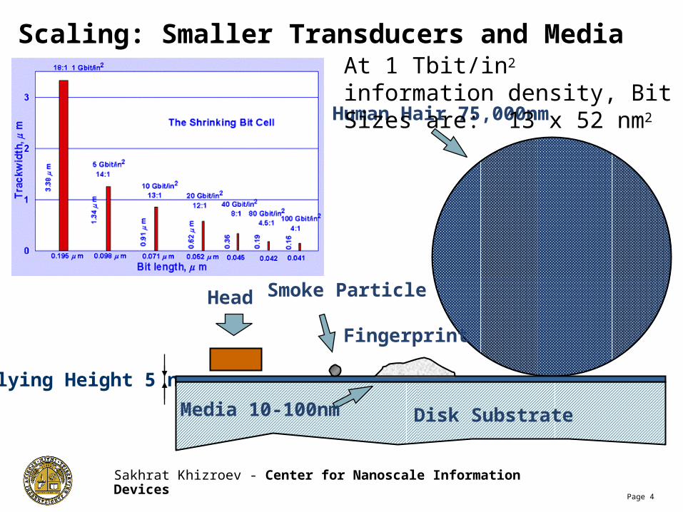
Scaling: Smaller Transducers and Media
Flying Height 5 nm
Head Smoke Particle
Fingerprint
Human Hair 75,000nm
Media 10-100nm Disk Substrate
At 1 Tbit/in2 information density, Bit Sizes are: 13 x 52 nm2
Sakhrat Khizroev - Center for Nanoscale Information DevicesPage 5
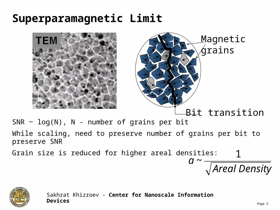
Superparamagnetic Limit
Magneticgrains
Bit transitionSNR ~ log(N), N - number of grains per bit
While scaling, need to preserve number of grains per bit to preserve SNR
Grain size is reduced for higher areal densities:
DensityAreala
1~
Sakhrat Khizroev - Center for Nanoscale Information DevicesPage 6
-45 0 45 90 135 180 225
-0.5
0.0
0.5
1.0
1.5
2.0
E+
E-
Ene
rgy,
eVMagnetization angle
H
megrain volu
energy anisotropy
E ,10-10~
k
Eexp
1290
B0
V
K
VKf
Tff
U
U
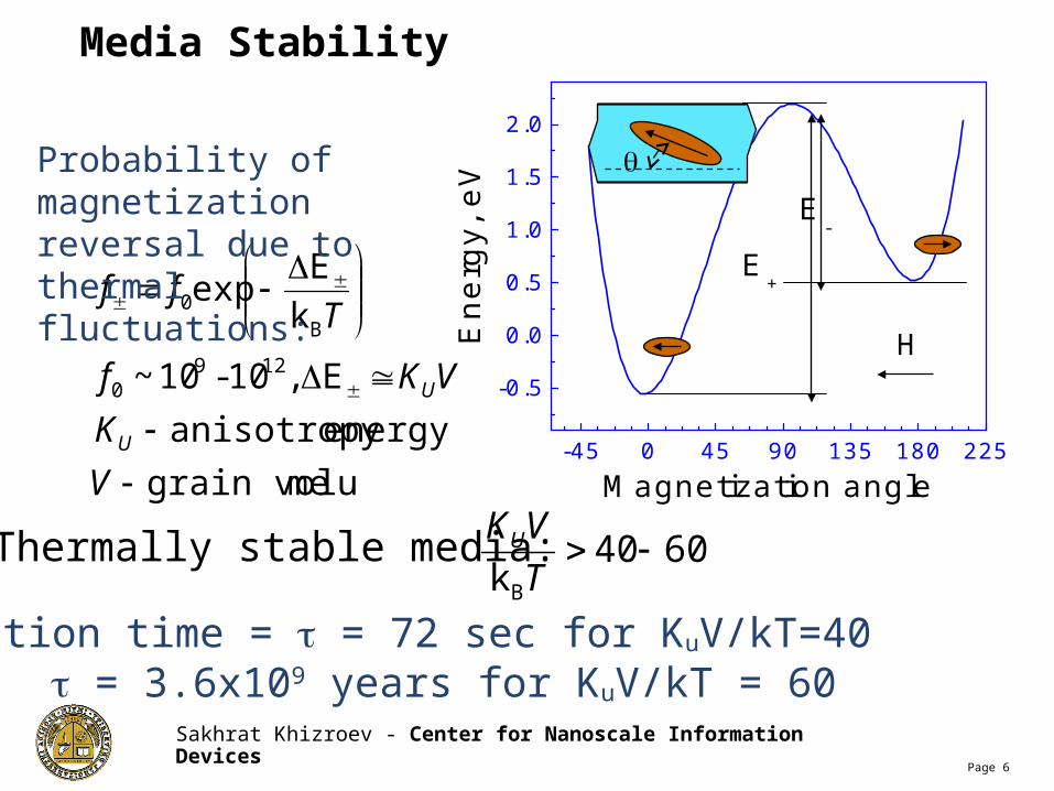
Probability of magnetization reversal due to thermal fluctuations:
6040kB
T
VKUThermally stable media:
Relaxation time = = 72 sec for KuV/kT=40 = 3.6x10⁹ years for KuV/kT = 60
Media Stability
Sakhrat Khizroev - Center for Nanoscale Information DevicesPage 7
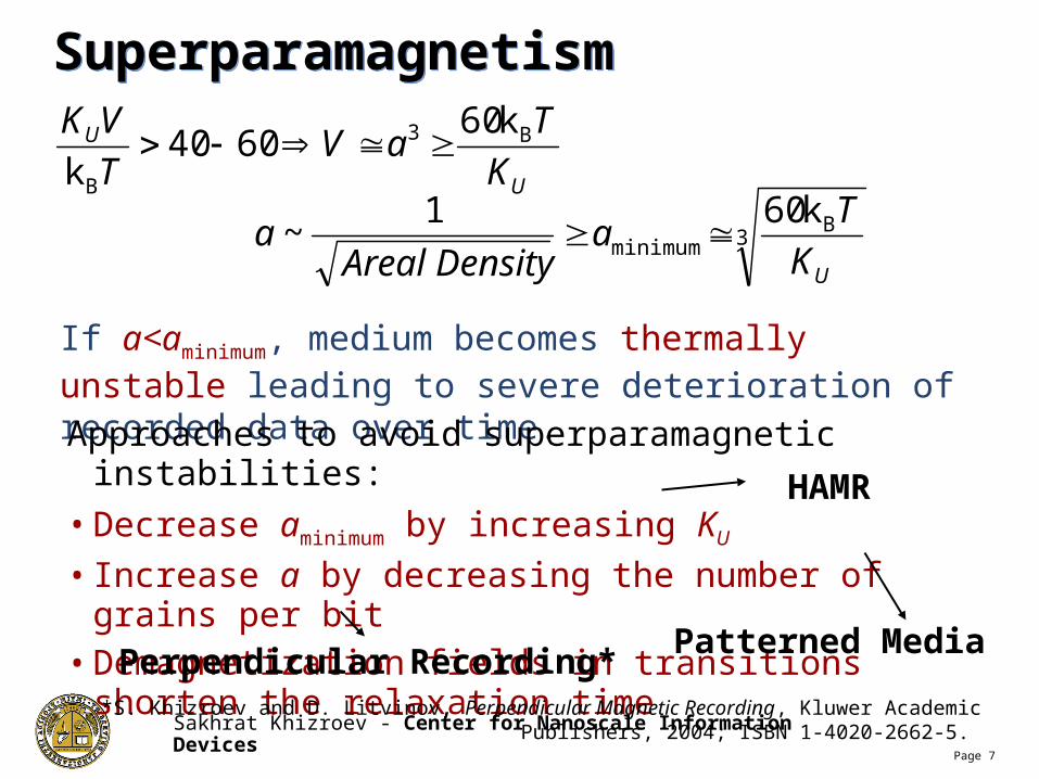
SuperparamagnetismSuperparamagnetism
U
U
K
TaV
T
VK B3
B
k606040
k
3B
minimum
k60
1~
UK
Ta
DensityAreala
If a<aminimum, medium becomes thermally unstable leading to severe deterioration of recorded data over time.Approaches to avoid superparamagnetic instabilities:
• Decrease aminimum by increasing KU
• Increase a by decreasing the number of grains per bit• Demagnetization fields in transitions shorten the
relaxation timePerpendicular Recording*
Patterned Media
HAMR
*S. Khizroev and D. Litvinov, Perpendicular Magnetic Recording, Kluwer Academic Publishers, 2004; ISBN 1-4020-2662-5.
Sakhrat Khizroev - Center for Nanoscale Information DevicesPage 8
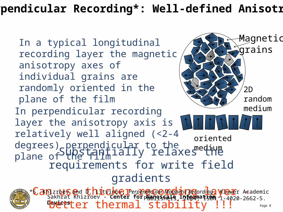
In a typical longitudinal recording layer the magnetic anisotropy axes of individual grains are randomly oriented in the plane of the film
In perpendicular recording layer the anisotropy axis is relatively well aligned (<2-4 degrees) perpendicular to the plane of the film
Magneticgrains
2D random medium
oriented medium
Substantially relaxes the requirements for write field gradientsCan use thicker recording layer - better thermal stability !!!
(increased V in KUV/kBT ratio)
Perpendicular Recording*: Well-defined Anisotropy
*S. Khizroev and D. Litvinov, Perpendicular Magnetic Recording, Kluwer Academic Publishers, 2004; ISBN 1-4020-2662-5.
Sakhrat Khizroev - Center for Nanoscale Information DevicesPage 9
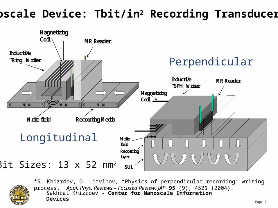
Nanoscale Device: Tbit/in2 Recording Transducer*
S N N S N SS N S NN S
Inductive“Ring” Writer
MR Reader
MagnetizingCoil
Write field Recording Media
Inductive“SPH” Writer
MR Reader
MagnetizingCoil
Recordinglayer
SUL
Writefield
Longitudinal
Perpendicular
Bit Sizes: 13 x 52 nm2
*S. Khizroev, D. Litvinov, “Physics of perpendicular recording: writing process,” Appl. Phys. Reviews – Focused Review, JAP 95 (9), 4521 (2004).
Sakhrat Khizroev - Center for Nanoscale Information DevicesPage 10
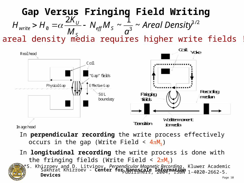
In perpendicular recording the write process effectively occurs in the gap (Write Field < 4MS)
In longitudinal recording the write process is done with the fringing fields (Write Field < 2MS)
Gap Versus Fringing Field Writing2/3
30 ~1
~2
DensityAreala
MNM
KHH Seff
S
Uwrite Higher areal density media requires higher write fields !!!
*S. Khizroev and D. Litvinov, Perpendicular Magnetic Recording, Kluwer Academic Publishers, 2004; ISBN 1-4020-2662-5.
Sakhrat Khizroev - Center for Nanoscale Information DevicesPage 11
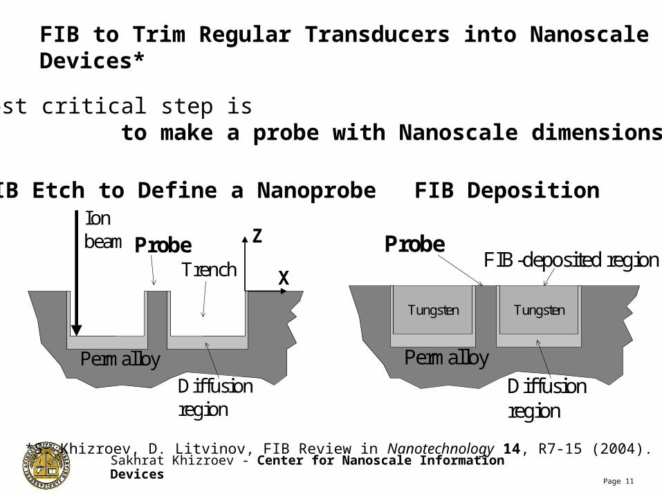
FIB to Trim Regular Transducers into Nanoscale Devices*
Z
X
Ionbeam
Permalloy
Diffusionregion
ProbeTrench
FIB Etch to Define a Nanoprobe
Permalloy
Diffusionregion
ProbeFIB-deposited region
TungstenTungsten
FIB Deposition
The most critical step is to make a probe with Nanoscale dimensions
*S. Khizroev, D. Litvinov, FIB Review in Nanotechnology 14, R7-15 (2004).
Sakhrat Khizroev - Center for Nanoscale Information DevicesPage 12
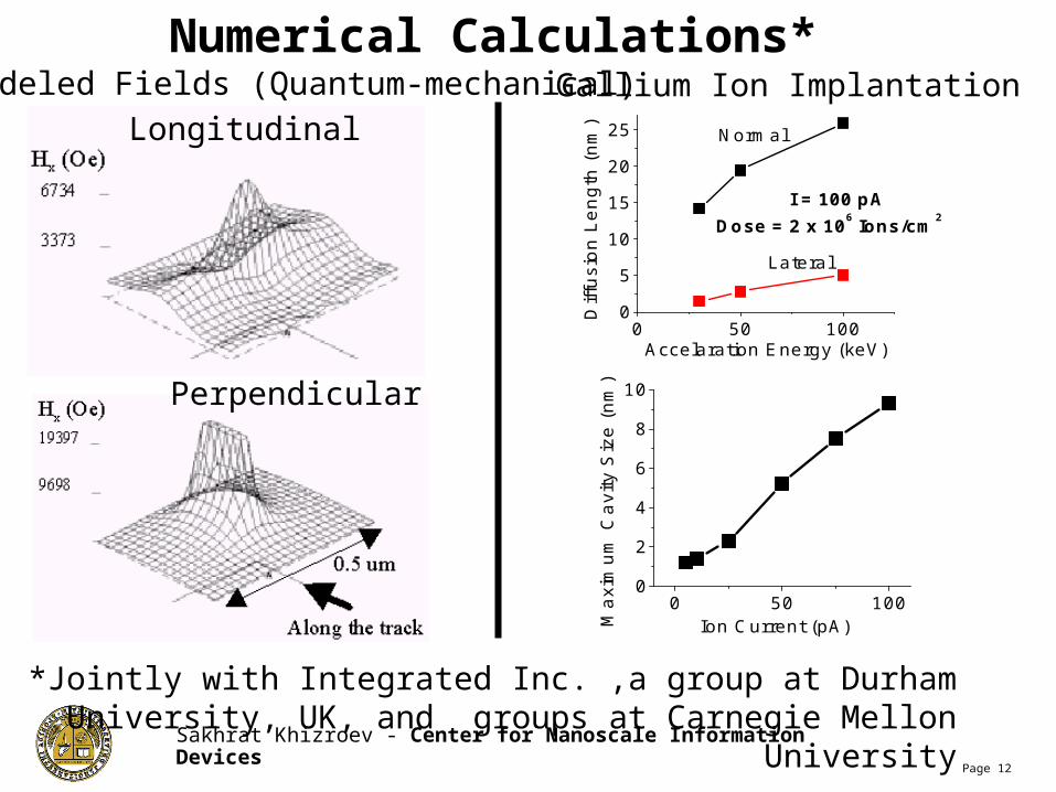
Numerical Calculations*
*Jointly with Integrated Inc. ,a group at Durham University, UK, and groups at Carnegie Mellon University
Longitudinal
Perpendicular
Modeled Fields (Quantum-mechanical) Gallium Ion Implantation
0 50 1000
5
10
15
20
25
Dose = 2 x 10⁶ Ions/cm2
Lateral
Normal
Diff
usio
n Le
ngth
(nm
)
I = 100 pA
Accelaration Energy (keV)
0 50 1000
2
4
6
8
10
Max
imum
Cav
ity S
ize
(nm
)Ion Current (pA)
Sakhrat Khizroev - Center for Nanoscale Information DevicesPage 13
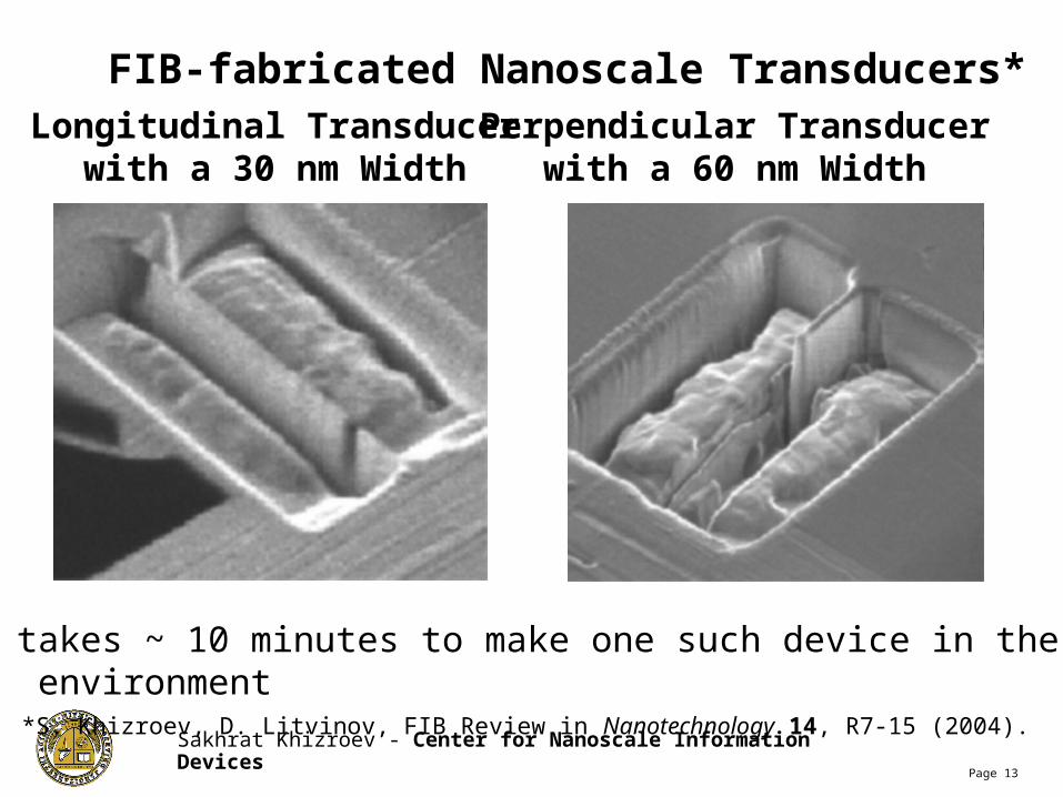
Longitudinal Transducerwith a 30 nm Width
Perpendicular Transducerwith a 60 nm Width
FIB-fabricated Nanoscale Transducers*
Note: It takes ~ 10 minutes to make one such device in the University environment
*S. Khizroev, D. Litvinov, FIB Review in Nanotechnology 14, R7-15 (2004).
Sakhrat Khizroev - Center for Nanoscale Information DevicesPage 14
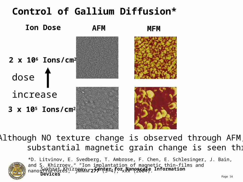
Control of Gallium Diffusion*
AFM MFM
3 x 10⁵ Ions/cm2
2 x 10⁶ Ions/cm2
Ion Dose
NOTE: Although NO texture change is observed through AFM, substantial magnetic grain change is seen through MFM
dose
increase
*D. Litvinov, E. Svedberg, T. Ambrose, F. Chen, E. Schlesinger, J. Bain, and S. Khizroev, “Ion implantation of magnetic thin-films and nanostructures,” JMMM 277 (3-4), xxx (2004).
Sakhrat Khizroev - Center for Nanoscale Information DevicesPage 15
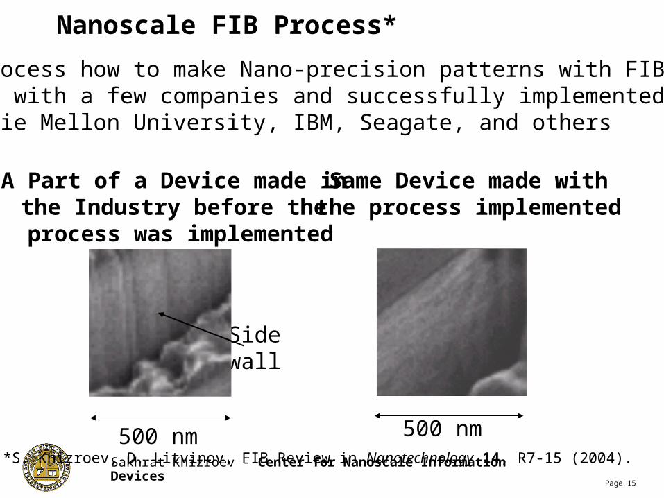
The process how to make Nano-precision patterns with FIB wasshared with a few companies and successfully implemented by:Carnegie Mellon University, IBM, Seagate, and others
500 nm500 nm
Sidewall
A Part of a Device made in the Industry before the
process was implemented
Same Device made withthe process implemented
Nanoscale FIB Process*
*S. Khizroev, D. Litvinov, FIB Review in Nanotechnology 14, R7-15 (2004).
Sakhrat Khizroev - Center for Nanoscale Information DevicesPage 16
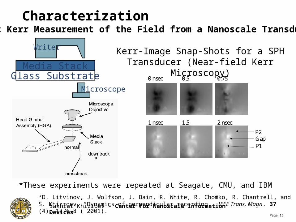
0 nsec 0.5 0.75
1 nsec 1.5 2 nsec
P2GapP1
Dynamic Kerr Measurement of the Field from a Nanoscale Transducer*Characterization
Kerr-Image Snap-Shots for a SPH Transducer (Near-field Kerr Microscopy)
Glass SubstrateMedia Stack
Microscope
Writer
*These experiments were repeated at Seagate, CMU, and IBM
*D. Litvinov, J. Wolfson, J. Bain, R. White, R. Chomko, R. Chantrell, and S. Khizroev, “Dynamics of perpendicular recording,” IEEE Trans. Magn. 37 (4), 1376-8 ( 2001).
Sakhrat Khizroev - Center for Nanoscale Information DevicesPage 17
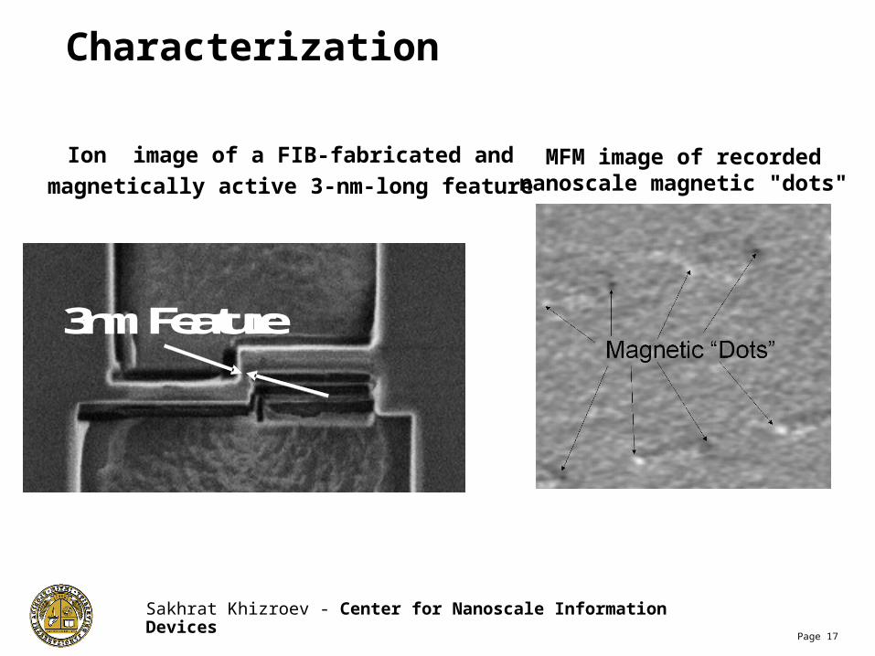
Characterization
3nm Feature
(a) (b)
3nm Feature
(a) (b)
Ion image of a FIB-fabricated and
magnetically active 3-nm-long feature MFM image of recorded
nanoscale magnetic "dots"

Sakhrat Khizroev - Center for Nanoscale Information DevicesPage 18
Perpendicular Recording with Bit Widths of less than 65 nm*
130 nm
~400 ktpiCoB/Pd multilayer
CoCrPtTa alloy~190 ktpi
Current “state-of-the-art” longitudinal recording is <100ktpi
400 nm
Writer
Reader
MFM Images of Nanoscale Size Information
*S. Khizroev, D. A. Thompson, M. H. Kryder, and D. Litvinov, Appl. Phys. Lett. 81 (12), 2256 (2002); Editor's choice for the Virtual Journal of Nanoscale Science & Technology, Sep 23rd 2002.
The FIB-made transducer
Sakhrat Khizroev - Center for Nanoscale Information DevicesPage 19
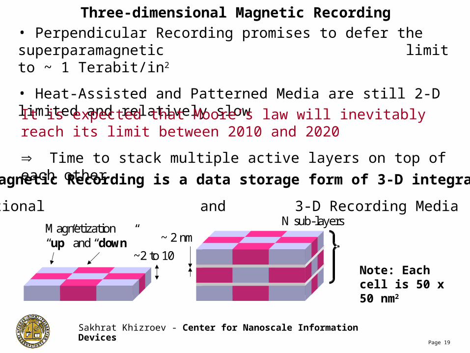
• Perpendicular Recording promises to defer the superparamagnetic limit to ~ 1 Terabit/in2
• Heat-Assisted and Patterned Media are still 2-D limited and relatively slow
It is expected that Moore’s law will inevitably reach its limit between 2010 and 2020
Time to stack multiple active layers on top of each other
3-D Magnetic Recording is a data storage form of 3-D integration
Conventional and 3-D Recording Media
(a) (b)
~2 to 10
~ 2 nmN sub-layers
Magnetization “up” and “down”
Note: Each cell is 50 x 50 nm2
Three-dimensional Magnetic Recording

Sakhrat Khizroev - Center for Nanoscale Information DevicesPage 20
3-D Magnetic Recording
The development of 3-D magnetic recording is divided into two phases:
1. Multi-level Recording: not optimally utilized 3-D space
Note: Effective areal density increase is by a factor of Log2L (where L is the number of signal levels)
2. 3-D Recording: each magnetic layer is separately addressed
Note: Effective areal density increase is by a factor of N (where N is the number of recording layers)
N layerscontributingtogether to one level
n-th layer addressing
Note: Each cell is 50 x 50 nm2
Note: These are not active layers
Lead Ph.D. Graduate Student: Yazan Hijazi, Sakhrat Khizroev
Sakhrat Khizroev - Center for Nanoscale Information DevicesPage 21
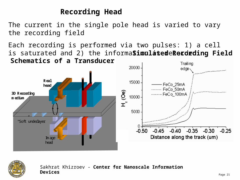
Recording Head
The current in the single pole head is varied to vary the recording field
Each recording is performed via two pulses: 1) a cell is saturated and 2) the information is recorded
Realhead
Imagehead
3D Recording medium
“Soft” underlayer
Schematics of a TransducerSimulated Recording Field
Sakhrat Khizroev - Center for Nanoscale Information DevicesPage 22
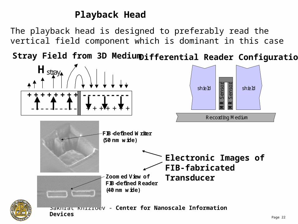
Playback Head
The playback head is designed to preferably read the vertical field component which is dominant in this case
++
charges in the transition
++
+ + + + + + + + - - - - - - - - - -
- - - - - - - - - - + + + + + + +
Hstray
Hstray
+ + + + + + + + - - - - - - - - - -
- - - - - - - - - - + + + + + + + Underlayerboundary
Mediumimage
M(a)
(b)
(c)
Stray Field from 3D Medium
Recording MediumRecording Medium
MR
Sen
sor
MR
Sen
sor
(c) (d)
shield shield
Recording MediumRecording MediumM
R S
enso
r
MR
Sen
sor
(a) (b)
shield shield
MR
Sen
sor
MR
Sen
sor
Differential Reader Configuration
FIB-defined Writer(50 nm wide)
Zoomed View of FIB-defined Reader(40 nm wide)
Electronic Images of FIB-fabricated Transducer
Sakhrat Khizroev - Center for Nanoscale Information DevicesPage 23
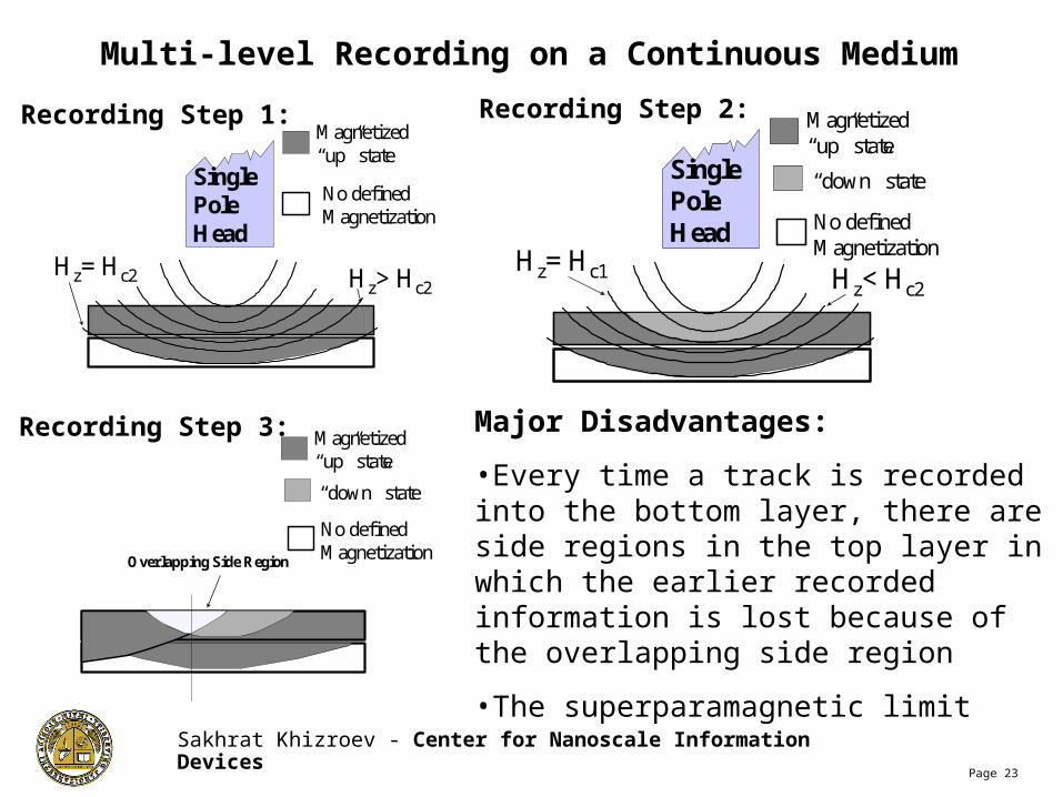
Multi-level Recording on a Continuous Medium
Hz> Hc2
SinglePoleHead
Hz= Hc2
Magnetized “up” state
No definedMagnetization
Hz< Hc2
SinglePoleHead
Hz= Hc1
Magnetized “up” state
No definedMagnetization
“down” state
Magnetized “up” state
No definedMagnetization
“down” state
Overlapping Side Region
Major Disadvantages:
•Every time a track is recorded into the bottom layer, there are side regions in the top layer in which the earlier recorded information is lost because of the overlapping side region
•The superparamagnetic limit
Recording Step 1: Recording Step 2:
Recording Step 3:
Sakhrat Khizroev - Center for Nanoscale Information DevicesPage 24
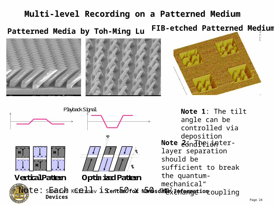
Multi-level Recording on a Patterned Medium
+ + + +
+ + + +
- - - -- - - -
M+ + + +
+ + + +
- - - -- - - -
M
+ + + +
+ + + +
- - - -
- - - -
M
tb
tt
Playback Signal
Vertical Pattern Optimized Pattern
Patterned Media by Toh-Ming Lu
Note 1: The tilt angle can be controlled via deposition condition
Note 2: The inter-layer separation should be sufficient to break the quantum-mechanical “exchange” coupling
FIB-etched Patterned Medium
Note: Each cell is ~50 x 50 nm2
Sakhrat Khizroev - Center for Nanoscale Information DevicesPage 25
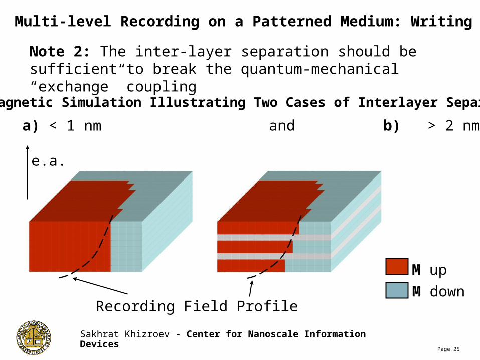
Multi-level Recording on a Patterned Medium: Writing
Note 2: The inter-layer separation should be sufficient to break the quantum-mechanical “exchange” coupling
Micromagnetic Simulation Illustrating Two Cases of Interlayer Separation:
a) < 1 nm and b) > 2 nm
Recording Field Profile
M up
M down
e.a.
Sakhrat Khizroev - Center for Nanoscale Information DevicesPage 26
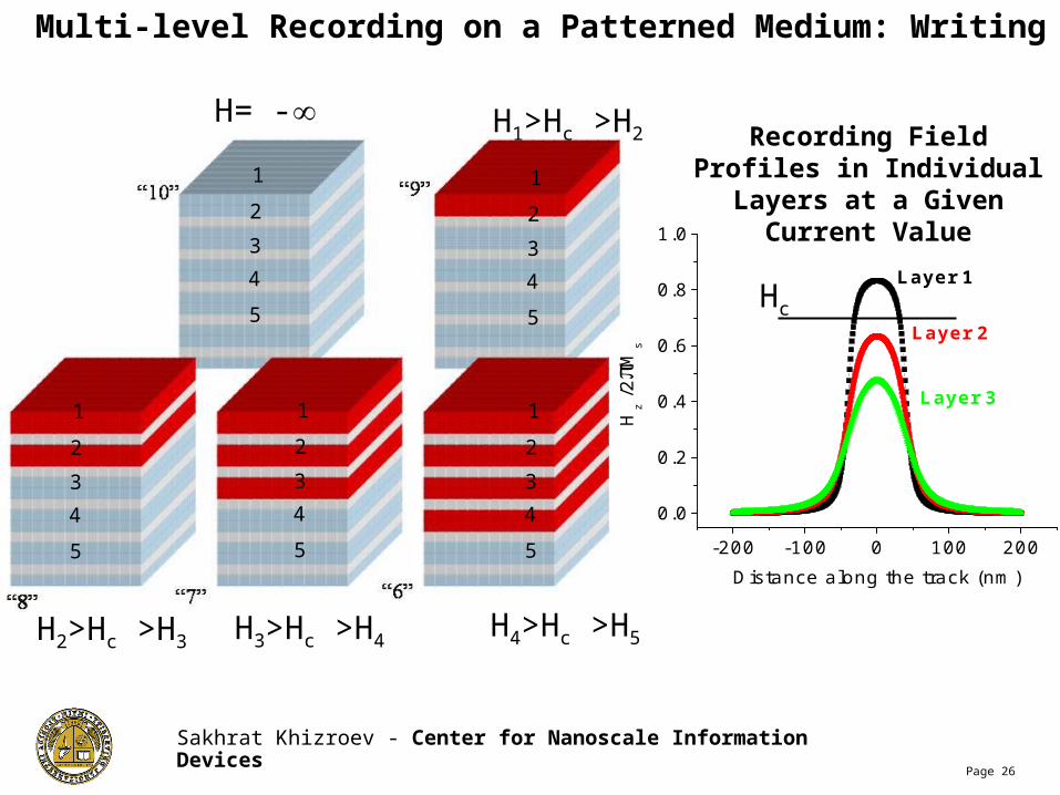
Multi-level Recording on a Patterned Medium: Writing
H= - H1>Hc >H2
H4>Hc >H5
1
2
3
4
5
1
2
3
4
5
1
2
3
4
5
1
2
3
4
5
1
2
3
4
5
H3>Hc >H4H2>Hc >H3
-200 -100 0 100 200
0.0
0.2
0.4
0.6
0.8
1.0
Layer 3
Layer 2
Layer 1
Hz /2
Ms
Distance along the track (nm)
Recording Field Profiles in Individual Layers at a Given
Current Value
Hc
Sakhrat Khizroev - Center for Nanoscale Information DevicesPage 27
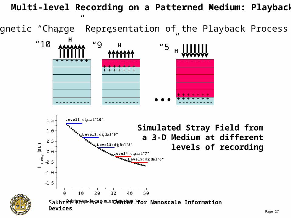
Multi-level Recording on a Patterned Medium: Playback
+ + + + + + +
- - - - - - - - - -
+ + + + + + +
- - - - - - - - - -
+ + + + + + +- - - - - - - - - -
... + + + + + + +- - - - - - - - - -
+ + + + + + +
- - - - - - - - - -
HH
H
Magnetic “Charge” Representation of the Playback Process
“10” “9” “5”
0 10 20 30 40 50
-1.5
-1.0
-0.5
0.0
0.5
1.0
1.5
Level 4: digital "7"Level 5: digital "6"
Level 3: digital "8"
Level 2: digital "9"
Level 1: digital "10"
Hz
stra
y (au
)
Distance in the medium (nm)
Simulated Stray Field from a 3-D Medium at different levels of
recording
Sakhrat Khizroev - Center for Nanoscale Information DevicesPage 28
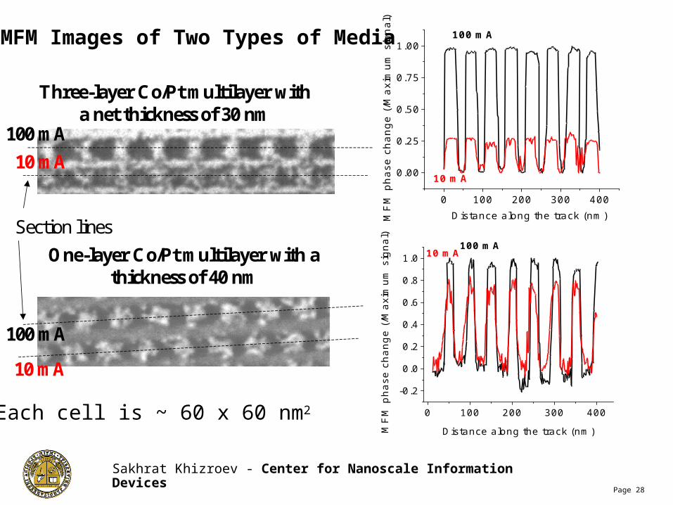
Section lines
Three-layer Co/Pt multilayer with a net thickness of 30 nm
One-layer Co/Pt multilayer with a thickness of 40 nm
10 mA
100 mA
100 mA
10 mA
0 100 200 300 400
-0.2
0.0
0.2
0.4
0.6
0.8
1.0 10 mA100 mA
MF
M p
hase
cha
nge
(/M
axim
um s
igna
l)
Distance along the track (nm)
0 100 200 300 400
0.00
0.25
0.50
0.75
1.00
10 mA
MF
M p
hase
cha
nge
(/M
axim
um s
igna
l)
100 mA
Distance along the track (nm)
MFM Images of Two Types of Media
Each cell is ~ 60 x 60 nm2

Sakhrat Khizroev - Center for Nanoscale Information DevicesPage 29
Note 2: The demagnetization field could be fairly large for some configuration. Special bit encoding should be considered to avoid the unfavorable bit configuration.
Hdemag >> 4Ms
SNR Limitations
1 2 3 4 5
4
6
8
10
12
14
16
18
20
22
SN
R (
dB
)
Number of Layers
Patterned Media (ideally, fabrication technique limited)
Electronic noise sources are 10 Ohm GMR Sensor and 0.2 nV/sqrt(Hz) preamp noise over a 500 MHz CTF bandwidth at 1 Gbit/sec
Note 1: Special encoding channels should be used to reduce BER
Sakhrat Khizroev - Center for Nanoscale Information DevicesPage 30
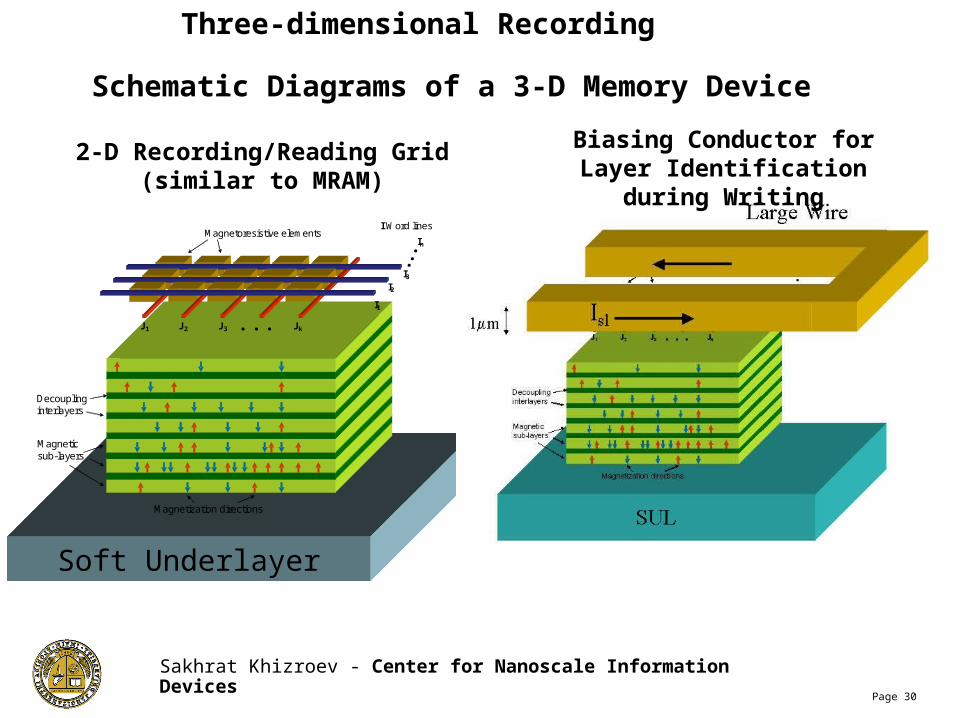
Soft Underlayer
Magneticsub-layers
Decouplinginterlayers
Magnetization directions
Magnetoresistive elementsI Word lines
I1
I2
I3
In
...
J1 J2 J3 Jk. . .
Three-dimensional Recording
Schematic Diagrams of a 3-D Memory Device
Biasing Conductor for Layer Identification during Writing
2-D Recording/Reading Grid (similar to MRAM)
Sakhrat Khizroev - Center for Nanoscale Information DevicesPage 31
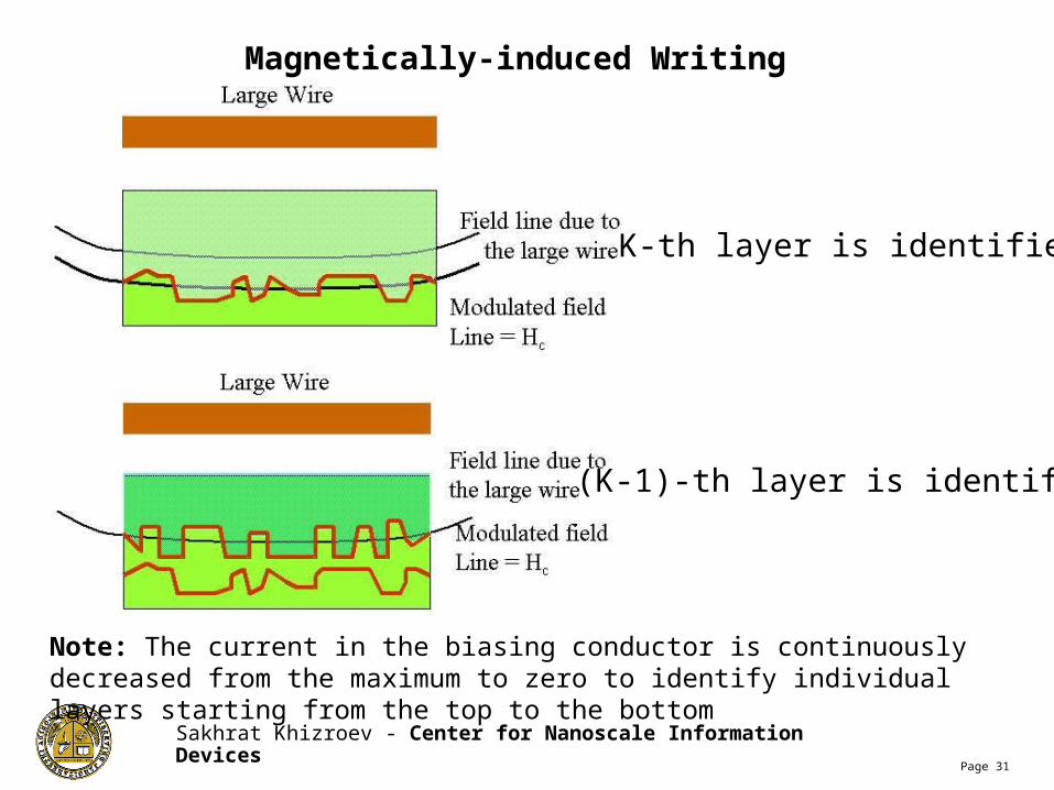
Magnetically-induced Writing
Note: The current in the biasing conductor is continuously decreased from the maximum to zero to identify individual layers starting from the top to the bottom
K-th layer is identified
(K-1)-th layer is identified
Sakhrat Khizroev - Center for Nanoscale Information DevicesPage 32
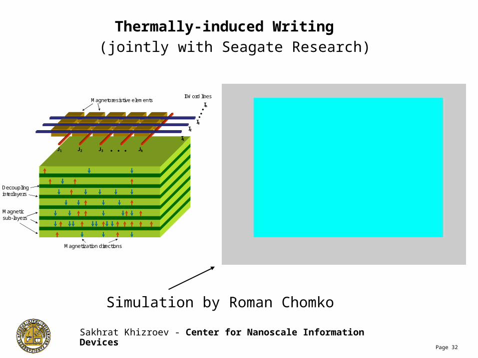
Thermally-induced Writing
Magneticsub-layers
Decouplinginterlayers
Magnetization directions
Magnetoresistive elementsI Word lines
I1
I2
I3
In
...
J1 J2 J3 Jk. . .
Simulation by Roman Chomko
(jointly with Seagate Research)
Sakhrat Khizroev - Center for Nanoscale Information DevicesPage 33
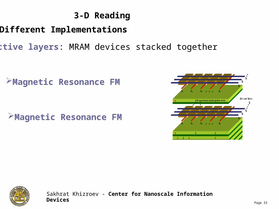
3-D Reading
Active layers: MRAM devices stacked together
Different Implementations
Magneticsub-layers
Decouplinginterlayers
Magnetization directions
Magnetoresistive elementsI Word lines
I1
I2
I3
In
...
J1 J2 J3 Jk. . .
Magneticsub-layers
Decouplinginterlayers
Magnetization directions
Magnetoresistive elementsI Word lines
I1
I2
I3
In
...
J1 J2 J3 Jk. . .
Magnetic Resonance FM
CoCrPtTa alloyMagnetic Resonance FM
Sakhrat Khizroev - Center for Nanoscale Information DevicesPage 34
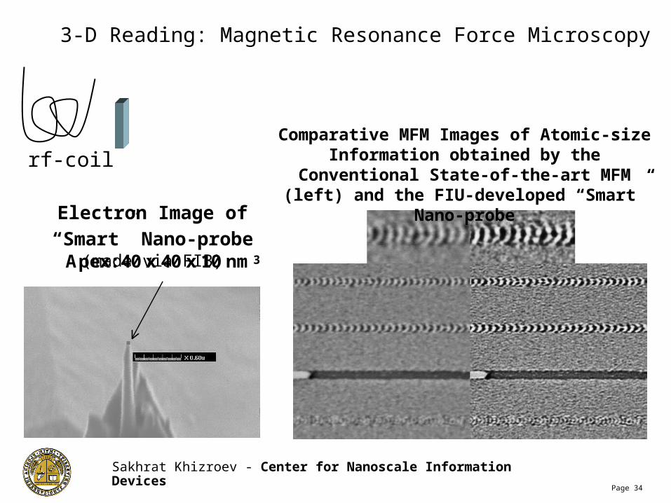
CoCrPtTa alloy
Apex: 40 x 40 x 10 nm3
Electron Image of “Smart”
Nano-probe (made via FIB)
Comparative MFM Images of Atomic-size Information obtained by the Conventional State-of-the-art MFM (left) and the FIU-developed “Smart”
Nano-probe
3-D Reading: Magnetic Resonance Force Microscopy
rf-coil

Sakhrat Khizroev - Center for Nanoscale Information DevicesPage 35
3-D Reading: Magnetically-induced Reading*
Note 1: Through the variation of the “softness” of the SUL, one can vary the sensitivity field of each cell
-0.10 -0.05 0.00 0.05 0.10
0
50
100
150
Hz (
au)
Distance along X, m
Sensitivity Field with a “Free” SUL (red) and “Saturated” SUL (black)
rrMrrHS zz
)()(~According to the Reciprocity principle, the signal in each cell is given by Expression
Note 2: Effective physical scanning in the vertical direction is produced via the variation of the “softness” of the SUL. Thus, each layer could be independently addressed
*Provisional patent filed with US PTO on August 4th 2004
Sakhrat Khizroev - Center for Nanoscale Information DevicesPage 36
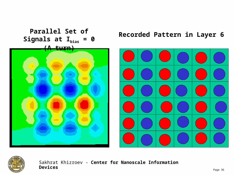
Recorded Pattern in Layer 6Parallel Set of Signals at Ibias = 0 (A turn)

Sakhrat Khizroev - Center for Nanoscale Information DevicesPage 37
Recorded Pattern in Layer 4Parallel Set of Signals at
Ibias = 1.56 (A turn)
Sakhrat Khizroev - Center for Nanoscale Information DevicesPage 38
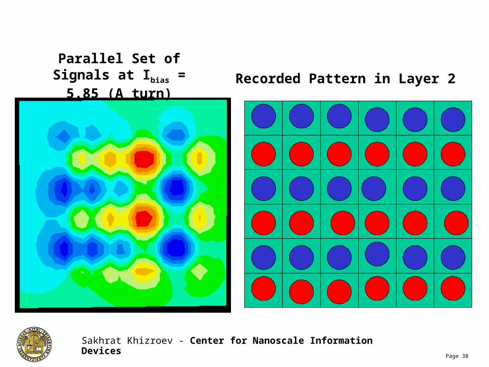
Recorded Pattern in Layer 2
Parallel Set of Signals at Ibias = 5.85 (A turn)
Sakhrat Khizroev - Center for Nanoscale Information DevicesPage 39
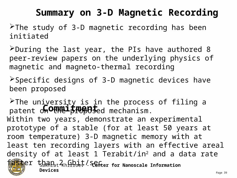
Summary on 3-D Magnetic Recording
The study of 3-D magnetic recording has been initiated
During the last year, the PIs have authored 8 peer-review papers on the underlying physics of magnetic and magneto-thermal recording
Specific designs of 3-D magnetic devices have been proposed
The university is in the process of filing a patent on the proposed mechanism.
CommitmentWithin two years, demonstrate an experimental prototype of a stable (for at least 50 years at room temperature) 3-D magnetic memory with at least ten recording layers with an effective areal density of at least 1 Terabit/in2 and a data rate faster than 2 Gbit/sec
Sakhrat Khizroev - Center for Nanoscale Information DevicesPage 40
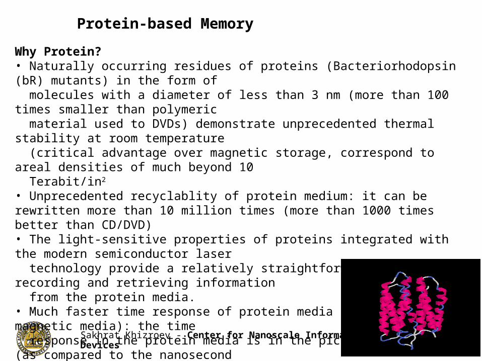
Protein-based Memory
Why Protein?• Naturally occurring residues of proteins (Bacteriorhodopsin (bR) mutants) in the form of molecules with a diameter of less than 3 nm (more than 100 times smaller than polymeric material used to DVDs) demonstrate unprecedented thermal stability at room temperature (critical advantage over magnetic storage, correspond to areal densities of much beyond 10 Terabit/in2 • Unprecedented recyclablity of protein medium: it can be rewritten more than 10 million times (more than 1000 times better than CD/DVD) • The light-sensitive properties of proteins integrated with the modern semiconductor laser technology provide a relatively straightforward control of recording and retrieving information from the protein media. • Much faster time response of protein media (as compared to magnetic media): the time response in the protein media is in the picosecond region (as compared to the nanosecond region in magnetic media) • Economical• Non-volatile
Sakhrat Khizroev - Center for Nanoscale Information DevicesPage 41
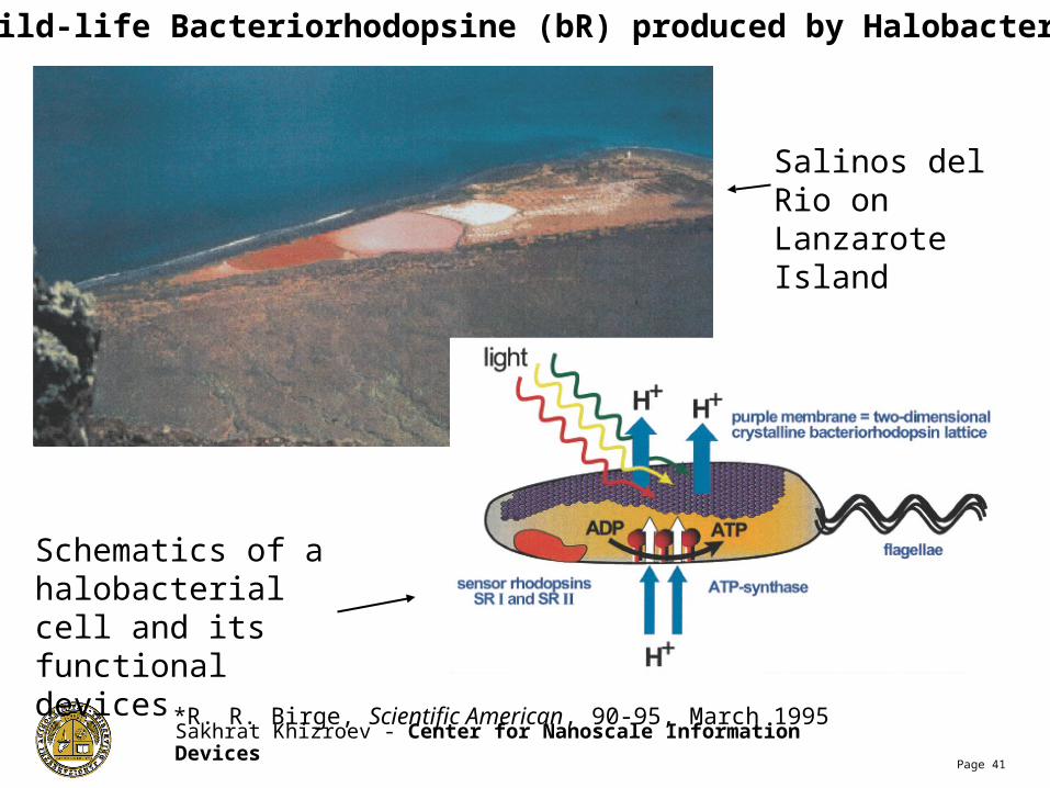
*R. R. Birge, Scientific American, 90-95, March 1995
Schematics of a halobacterial cell and its functional devices
Salinos del Rio on Lanzarote Island
Wild-life Bacteriorhodopsine (bR) produced by Halobacteria
Sakhrat Khizroev - Center for Nanoscale Information DevicesPage 42
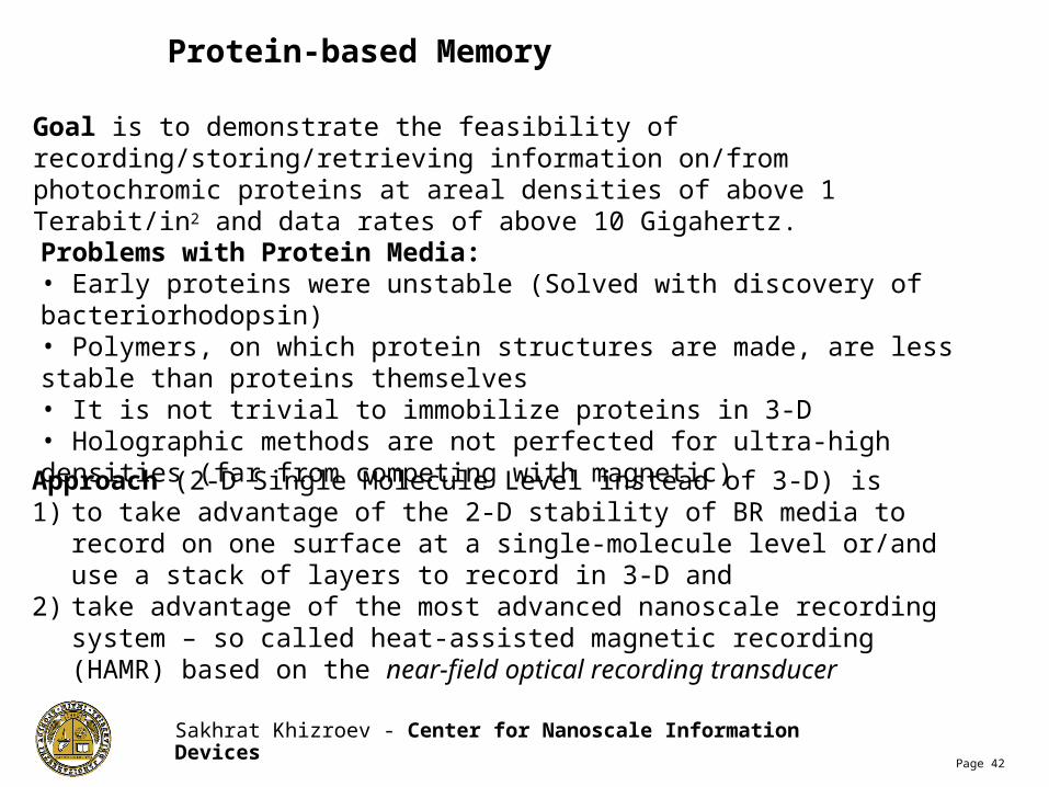
Goal is to demonstrate the feasibility of recording/storing/retrieving information on/from photochromic proteins at areal densities of above 1 Terabit/in2 and data rates of above 10 Gigahertz.
Approach (2-D Single Molecule Level instead of 3-D) is 1) to take advantage of the 2-D stability of BR media to record on one surface at
a single-molecule level or/and use a stack of layers to record in 3-D and 2) take advantage of the most advanced nanoscale recording system – so called
heat-assisted magnetic recording (HAMR) based on the near-field optical recording transducer
Protein-based Memory
Problems with Protein Media:• Early proteins were unstable (Solved with discovery of bacteriorhodopsin)• Polymers, on which protein structures are made, are less stable than proteins themselves• It is not trivial to immobilize proteins in 3-D• Holographic methods are not perfected for ultra-high densities (far from competing with magnetic)
Sakhrat Khizroev - Center for Nanoscale Information DevicesPage 43
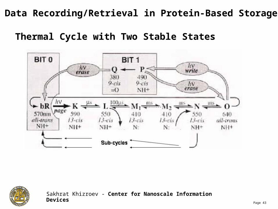
Data Recording/Retrieval in Protein-Based Storage
Thermal Cycle with Two Stable States
Sakhrat Khizroev - Center for Nanoscale Information DevicesPage 44
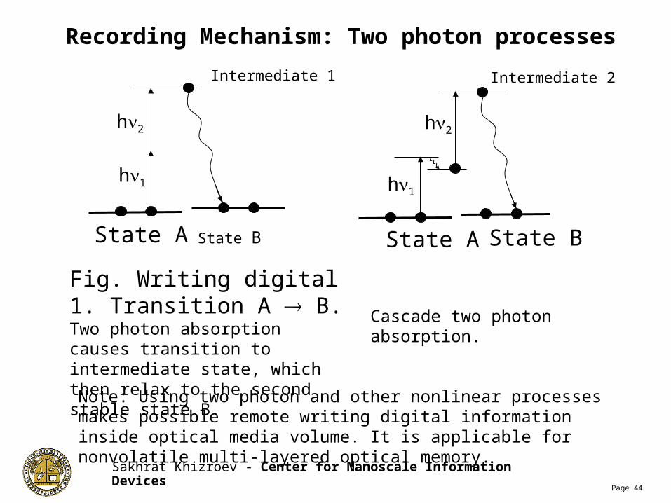
Fig. Writing digital 1. Transition A B.Two photon absorption causes transition to intermediate state, which then relax to the second stable state B.
Cascade two photon absorption.
h1
State A State B
Intermediate 1
h2 h2
State A State B
Intermediate 2
h1
Note: Using two photon and other nonlinear processes makes possible remote writing digital information inside optical media volume. It is applicable for nonvolatile multi-layered optical memory.
Recording Mechanism: Two photon processes

Sakhrat Khizroev - Center for Nanoscale Information DevicesPage 45
Earlier Proposed Protein Memory*
*R. R. Birge, Scientific American, 90-95, March 1995
Parallel Data Access (page by page via positioning of the green light)
Issues:•Optics never could record high densities
•3-D media are not trivial to immobilize
Sakhrat Khizroev - Center for Nanoscale Information DevicesPage 46
All the above-described methods of recording/retrieving data are quite complicated and it is hard to see whether they will be implemented and if yes, when. In fact, so far no physical demonstration of ultra-high density recording has been made!
The PIs propose first, to use a bit-by-bit 2-D type of recording to demonstrate the feasibility
of the protein-based storage (it is trivial to immobilize 2-D media); then, to apply one of the available parallel data recording/retrieving mechanism (e.g. holographic).
To accomplish this goal, the PIs use the transducer design earlier developed for heat-assisted magnetic recording (HAMR)*. HAMR is the most advanced recording mechanism proposed so far. The PIs have pioneered one of the most efficient design of the transducer for HAMR
The Proposed Solution to Demonstrate the Feasibility of Protein Based Storage
*T. McDaniel, W. Challener, “Issues in heat-assisted perpendicular recording,” IEEE Trans. Magn. 39 (4), 1972-9 (2003).
Sakhrat Khizroev - Center for Nanoscale Information DevicesPage 47
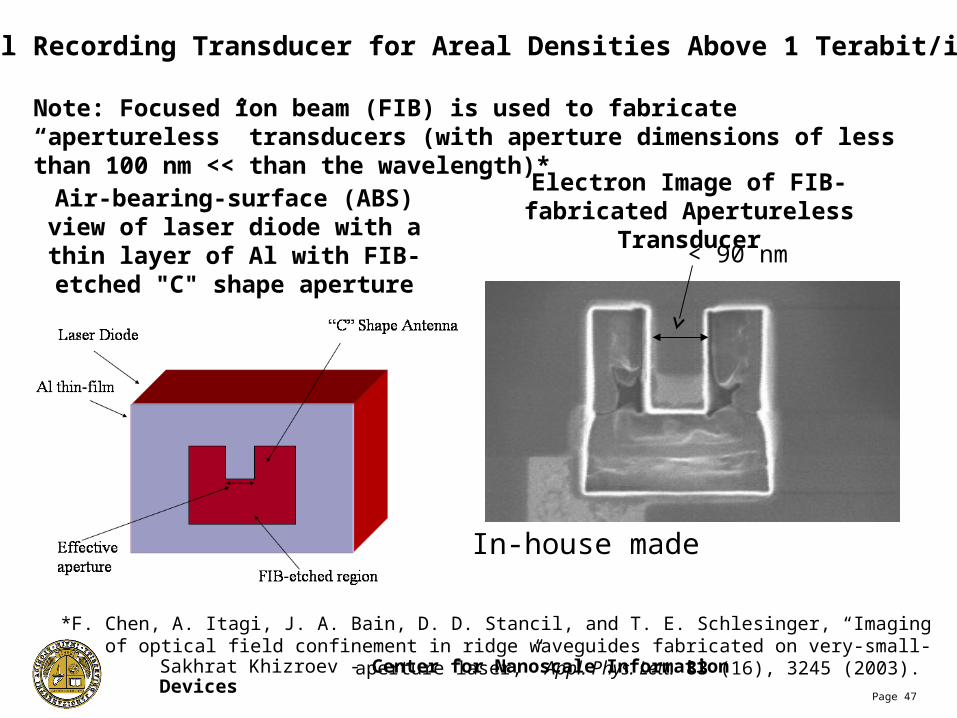
Air-bearing-surface (ABS) view of laser diode with a thin layer of Al
with FIB-etched "C" shape aperture
Novel Recording Transducer for Areal Densities Above 1 Terabit/in2
Electron Image of FIB-fabricated Apertureless Transducer
Note: Focused ion beam (FIB) is used to fabricate “apertureless” transducers (with aperture dimensions of less than 100 nm << than the wavelength)*
< 90 nm
In-house made
*F. Chen, A. Itagi, J. A. Bain, D. D. Stancil, and T. E. Schlesinger, “Imaging of optical field confinement in ridge waveguides fabricated on very-small-aperture laser,” Appl. Phys. Lett. 83 (16), 3245 (2003).
Sakhrat Khizroev - Center for Nanoscale Information DevicesPage 48
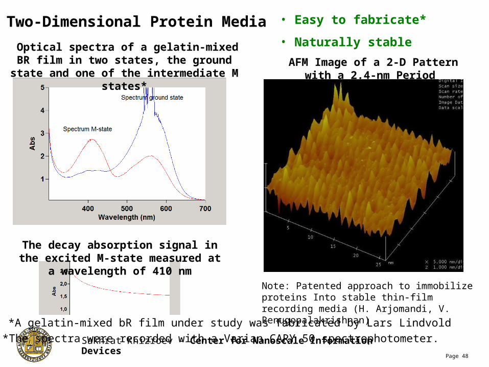
Two-Dimensional Protein Media • Easy to fabricate*
• Naturally stable Optical spectra of a gelatin-mixed BR film in two states, the ground state and one of the intermediate
M states*
*The spectra were recorded with a Varian CARY 50 spectrophotometer.
The decay absorption signal in the excited M-state measured at a wavelength of 410 nm
*A gelatin-mixed bR film under study was fabricated by Lars Lindvold
Note: Patented approach to immobilize proteins Into stable thin-film recording media (H. Arjomandi, V. Renugopalakrishnan)
AFM Image of a 2-D Pattern with a 2.4-nm Period
Sakhrat Khizroev - Center for Nanoscale Information DevicesPage 49
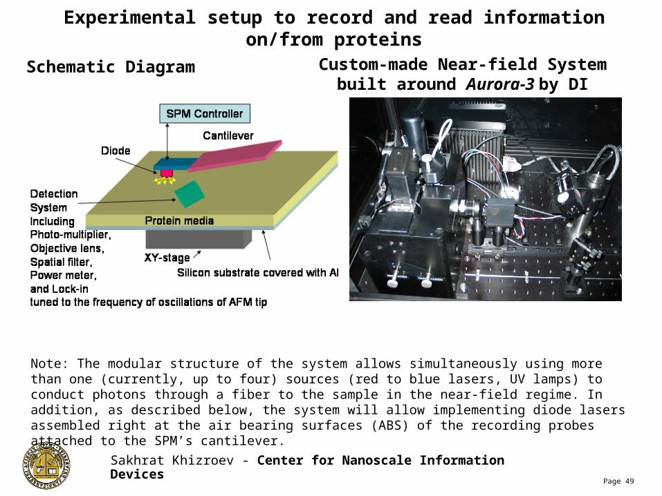
Custom-made Near-field System built around Aurora-3 by DI
Experimental setup to record and read information on/from proteins
Schematic Diagram
Note: The modular structure of the system allows simultaneously using more than one (currently, up to four) sources (red to blue lasers, UV lamps) to conduct photons through a fiber to the sample in the near-field regime. In addition, as described below, the system will allow implementing diode lasers assembled right at the air bearing surfaces (ABS) of the recording probes attached to the SPM’s cantilever.
Sakhrat Khizroev - Center for Nanoscale Information DevicesPage 50
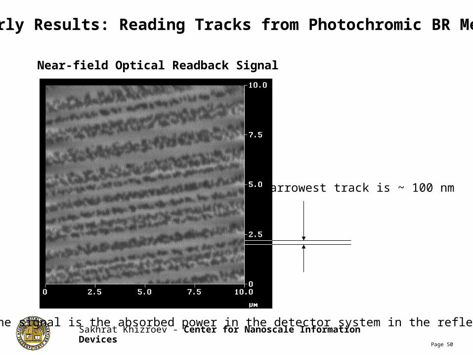
Early Results: Reading Tracks from Photochromic BR Media
* The signal is the absorbed power in the detector system in the reflection mode
Near-field Optical Readback Signal
Narrowest track is ~ 100 nm
Sakhrat Khizroev - Center for Nanoscale Information DevicesPage 51
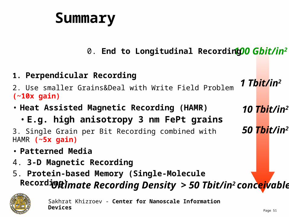
1 Tbit/in2
10 Tbit/in2
50 Tbit/in2
100 Gbit/in2
1. Perpendicular Recording
2. Use smaller Grains&Deal with Write Field Problem (~10x gain)
• Heat Assisted Magnetic Recording (HAMR)
• E.g. high anisotropy 3 nm FePt grains3. Single Grain per Bit Recording combined with HAMR (~5x gain)
• Patterned Media4. 3-D Magnetic Recording5. Protein-based Memory (Single-Molecule Recording)
Ultimate Recording Density > 50 Tbit/in2 conceivable
Summary
0. End to Longitudinal Recording