role of wireless sensor networks in forest fire prevention
TRANSCRIPT

ABREVATIONSMicrocontroller:
Symbol NameACC Accumulator
B B register
PSW Program status word
SP Stack pointer
DPTR Data pointer 2 bytes
DPL Low byte
DPH High byte
P0 Port0
P1 Port1
P2 Port2
P3 Port3
IP Interrupt priority control
IE Interrupt enable control
TMOD Timer/counter mode control
TCON Timer/counter control
T2CON Timer/counter 2 control
T2MOD Timer/counter mode2 control
TH0 Timer/counter 0high byte
TL0 Timer/counter 0 low byte
TH1 Timer/counter 1 high byte
TL1 Timer/counter 1 low byte
TH2 Timer/counter 2 high byte
TL2 Timer/counter 2 low byte
SCON Serial control
SBUF Serial data buffer
PCON Power control
1

FIGURE LOCATIONS
1. Fig 1 : Components of a typical linear power supply
2. Fig 2 : An electrical transformer
3. Fig 3 : A three terminal voltage regulator
4. Fig 4 : Functional block diagram of a microcontroller
5. Fig 5 : Oscillator and timing circuit
6. Fig 6 : Pin diagram of AT89C51
7. Fig 7 : Oscillator connections
8. Fig 8 : External clock drive configuration
9. Fig 9 : RAM allocations in the 8051
10. Fig 10 : 8051 Register banks and their RAM addresses
11. Fig 11 : A MAX 232 integrated cicuit
12. Fig 12 : MAX 232(A) DIP package
13. Fig 13 : Pin description of the transmitter module
14. Fig 14 : Interfacing Transmitter module to a microcontroller
15. Fig 15 : Block diagram of HT12E Encoder
16. Fig 16 : Pin description of HT12E Encoder
17. Fig 17 : Timing diagram of the HT12E and HT12E
18. Fig 18 : Application circuit of HT12E
19. Fig 19 : Flow chart for data transmission HT12E
20. Fig 20 : RF receiver module
21. Fig 21 : Block diagram of HT12D decoder
22. Fig 22 : Pin diagram of HT12D
23. Fig 23 : Timing diagram of decoder HT12D
24. Fig 24 : Application of HT12D
25. Fig 25 : Flowchart of H12D for data transmission
2

1. INTRODUCTION
1.1 EMBEDDED SYSTEM:
An embedded system is a special-purpose system in which the computer is
completely encapsulated by or dedicated to the device or system it controls. Unlike a
general-purpose computer, such as a personal computer, an embedded system performs
one or a few predefined tasks, usually with very specific requirements. Since the system
is dedicated to specific tasks, design engineers can optimize it, reducing the size and cost
of the product. Embedded systems are often mass-produced, benefiting from economies
of scale.
Personal digital assistants (PDAs) or handheld computers are generally
considered embedded devices because of the nature of their hardware design, even
though they are more expandable in software terms. This line of definition continues to
blur as devices expand. With the introduction of the OQO Model 2 with the Windows XP
operating system and ports such as a USB port — both features usually belong to
"general purpose computers", — the line of nomenclature blurs even more.
Physically, embedded systems ranges from portable devices such as digital
watches and MP3 players, to large stationary installations like traffic lights, factory
controllers, or the systems controlling nuclear power plants.
In terms of complexity embedded systems can range from very simple with a
single microcontroller chip, to very complex with multiple units, peripherals and
networks mounted inside a large chassis or enclosure.
3

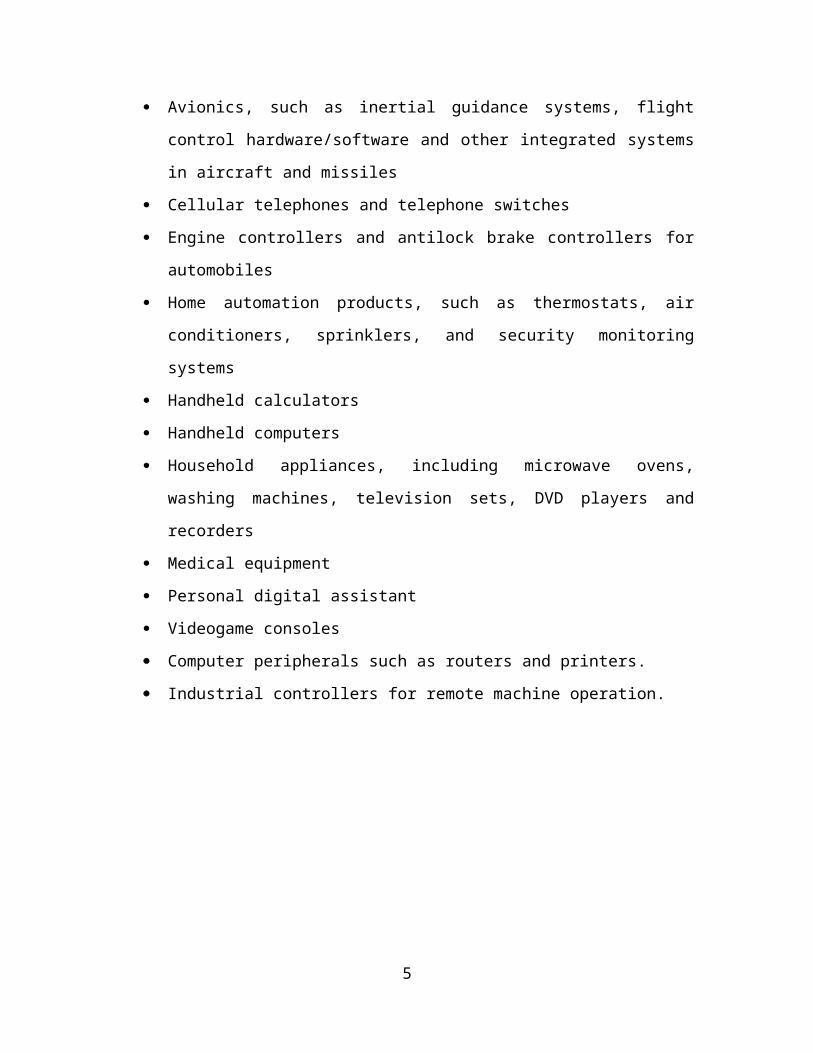
1.2 Examples of Embedded Systems: Avionics, such as inertial guidance systems, flight control hardware/software and
other integrated systems in aircraft and missiles
Cellular telephones and telephone switches
Engine controllers and antilock brake controllers for automobiles
Home automation products, such as thermostats, air conditioners, sprinklers, and
security monitoring systems
Handheld calculators
Handheld computers
Household appliances, including microwave ovens, washing machines, television
sets, DVD players and recorders
Medical equipment
Personal digital assistant
Videogame consoles
Computer peripherals such as routers and printers.
Industrial controllers for remote machine operation.
4
2. BLOCK DIAGRAM
Transmitter
5
MCU
Power Supply
PC
Decoder Parallel port
RF Rx.
EncoderSensors
RF Tx
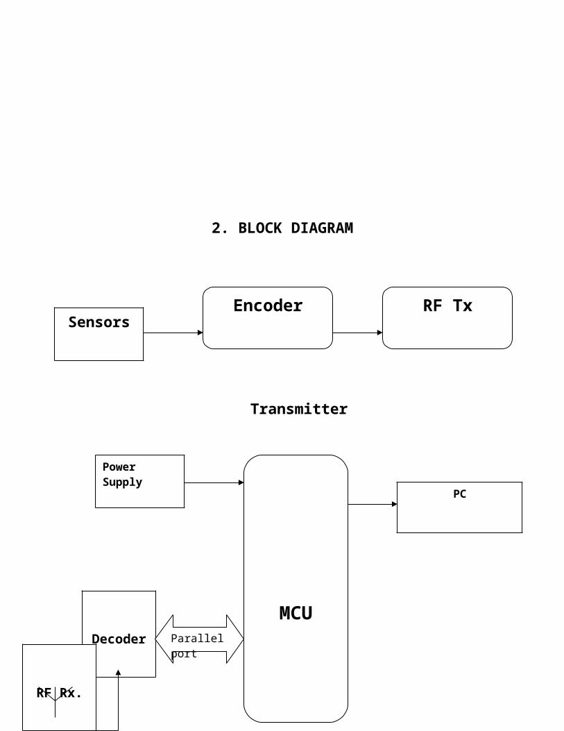
Reciever
3. BLOCK DIAGRAM EXPLANATION
Sensors:This block contains a ire sensor which is used to detect the fire in its range.
Output of this block is passed to transmitter to pass the information to the central station.
Encoder:A 16-bit address and 8-bit data encoder is used in this block. This encoder gives
the address of the destination along with the data in the format to pass the information to
the RF transmitter.
RF Tx:Radio frequency transmitter with 433 MHz. is use in this block to transmit the
data. This transmitter uses ASK modulation for transmitting.
Power supply: Power supply block contains step down transformer, rectifier and regulator. These
arrangements are used to supply the voltage to the all blocks of this system. The main
function of this block is to convert the 230V AC supply to 5V and 12V DC supply.
MCU:This block contains microcontroller. This is the heart of the receiver part. This
part takes the data from the microcontroller and takes the decision to blow the alarm r
not. And the same data will be passed to the PC for further assistance.
RF RX:Radio frequency receiver with 433 MHz. is use in this block to receive the data.
This receiver uses ASK demodulation for collecting.
Decode:
6

A 16-bit address and 8-bit data decoder is used in this block. This decoder
matches the address of the destination. After that the data is collected and it is passed to
the microcontroller through parallel communication
PC: The collected data from the node is passed through the microcontroller to the PC.
Between these two a interfacing device i.e. logic level converter is used. The data send to
the PC can be further transmits to any where using internet. So this block is a personal
computer.
7

4. SCHEMATIC
Schematic explanation:Firstly, the required operating voltage for Microcontroller 89C51 is 5V. Hence the
5V D.C. power supply is needed by the same. This regulated 5V is generated by first
stepping down the 230V to 9V by the step down transformer.
The step downed a.c. voltage is being rectified by the Bridge Rectifier.
The diodes used are 1N4007. The rectified a.c voltage is now filtered using a ‘C’ filter.
Now the rectified, filtered D.C. voltage is fed to the Voltage Regulator. This voltage
regulator allows us to have a Regulated Voltage which is +5V.The rectified; filtered and
regulated voltage is again filtered for ripples using an electrolytic capacitor 100μF. Now
the output from this section is fed to 40th pin of 89c51 microcontroller to supply operating
voltage.
The microcontroller 89c51 with Pull up resistors at Port0 and crystal oscillator of
11.0592 MHz crystal in conjunction with couple of capacitors of is placed at 18 th & 19th
pins of 89c51 to make it work (execute) properly.
In transmitter HT12E encoder IC is used. The data from the fire sensor is directly
attached to this IC. Fire sensor is arranged in a fixed bias circuit. This circuit is made up
of a transistor. One of the bridge arm is replaced with the fire sensor.
The function of HT12E IC is it takes the data from the data pins and club the data
with address and send it to the RF transmitter modules data in pin. The RF transmitter
contains ANT (antenna), data in, Vcc and GND pins.
At reviver side RF receiver is used to collect the data. This module also contains
dataout,VCC,GND and antenna pins. The data out pin is connected to the HT12D IC
which functions in a reverse manner of the HT12E. The data is passed to the
8

microcontroller from there. The controllers PORT1 pins are used for collecting data, so
these are used as input pins.
Pin no.10, & 9 are used for serial communication in microcontroller.
These two are connected to the MAX232 IC through this passed to the PC.
The microcontroller can communicate with the serial devices using its single
Serial Port. The logic levels at which this serial port operates is TTL logics. But some of
the serial devices operate at RS 232 Logic levels.
9

5. HARDWARE COMPONENTS
The Hardware components used in this project are
Regulated Power Supply
Microcontroller
Fire sensor
MAX 232
Buzzer
5.1 REGULATED POWER SUPPLY
The power supplies are designed to convert high voltage AC mains electricity to a
suitable low voltage supply for electronics circuits and other devices. A RPS (Regulated
Power Supply) is the Power Supply with Rectification, Filtering and Regulation being
done on the AC mains to get a Regulated power supply for Microcontroller and for the
other devices being interfaced to it.
A power supply can by broken down into a series of blocks, each of which performs a
particular function. A d.c power supply which maintains the output voltage constant
irrespective of a.c mains fluctuations or load variations is known as “Regulated D.C
Power Supply”
10

For example a 5V regulated power supply system as shown below:
Fig (1)
(i) Transformer: A transformer is an electrical device which is used to convert electrical
power from one Electrical circuit to another without change in frequency.
Transformers convert AC electricity from one voltage to another with little loss of power.
Transformers work only with AC and this is one of the reasons why mains electricity is
11

AC. Step-up transformers increase in output voltage, step-down transformers decrease in
output voltage. Most power supplies use a step-down transformer to reduce the
dangerously high mains voltage to a safer low voltage. The input coil is called the
primary and the output coil is called the secondary. There is no electrical connection
between the two coils; instead they are linked by an alternating magnetic field created in
the soft-iron core of the transformer. The two lines in the middle of the circuit symbol
represent the core. Transformers waste very little power so the power out is (almost)
equal to the power in. Note that as voltage is stepped down current is stepped up. The
ratio of the number of turns on each coil, called the turn’s ratio, determines the ratio of
the voltages. A step-down transformer has a large number of turns on its primary (input)
coil which is connected to the high voltage mains supply, and a small number of turns on
its secondary (output) coil to give a low output voltage.
Fig2: An Electrical Transformer
Turns ratio = Vp/ VS = Np/NS
Power Out= Power In
VS X IS=VP X IP
Vp = primary (input) voltage
Np = number of turns on primary coil
Ip = primary (input) current
12

(ii) RECTIFIER:
A circuit which is used to convert a.c to dc is known as RECTIFIER. The process of conversion a.c to d.c is called “rectification”
TYPES OF RECTIFIERS: Half wave Rectifier
Full wave rectifier
1. Centre tap full wave rectifier.
2. Bridge type full bridge rectifier.
Comparison of rectifier circuits:
Parameter Type of Rectifier
Half wave Full wave BridgeNumber of diodes
1 2
4
PIV of diodes Vm
2Vm
Vm
D.C output voltage Vm/z
2Vm/
2Vm/
Vdc,at no-load
0.318Vm
0.636Vm 0.636Vm
Ripple factor 1.21
0.482
0.482
Ripple frequency
f
2f
2f
Rectification efficiency
0.406
0.812
0.812
Transformer Utilization Factor(TUF)
0.287 0.693 0.812
RMS voltage Vrms Vm/2 Vm/√2 Vm/√2
13

Full-wave Rectifier:From the above comparison we came to know that full wave bridge rectifier as more
advantages than the other two rectifiers. So, in our project we are using full wave bridge
rectifier circuit.
Bridge Rectifier: A bridge rectifier makes use of four diodes in a bridge arrangement to
achieve full-wave rectification. This is a widely used configuration, both with individual
diodes wired as shown and with single component bridges where the diode bridge is
wired internally.
A bridge rectifier makes use of four diodes in a bridge arrangement as shown in
fig (a) to achieve full-wave rectification. This is a widely used configuration, both with
individual diodes wired as shown and with single component bridges where the diode
bridge is wired internally.
Fig (A)
14

Operation:During positive half cycle of secondary, the diodes D2 and D3 are in forward biased
while D1 and D4 are in reverse biased as shown in the fig(b). The current flow direction
is shown in the fig (b) with dotted arrows.
Fig (B)
During negative half cycle of secondary voltage, the diodes D1 and D4 are in forward
biased while D2 and D3 are in reverse biased as shown in the fig(c). The current flow
direction is shown in the fig (c) with dotted arrows.
Fig(C)
15

(iii) Filter: A Filter is a device which removes the a.c component of rectifier output
but allows the d.c component to reach the load
Capacitor Filter: We have seen that the ripple content in the rectified output of half wave rectifier is
121% or that of full-wave or bridge rectifier or bridge rectifier is 48% such high
percentages of ripples is not acceptable for most of the applications. Ripples can be
removed by one of the following methods of filtering.
(a) A capacitor, in parallel to the load, provides an easier by –pass for the ripples voltage
though it due to low impedance. At ripple frequency and leave the D.C. to appear at the
load.
(b) An inductor, in series with the load, prevents the passage of the ripple current (due to
high impedance at ripple frequency) while allowing the d.c (due to low resistance to d.c)
(c) Various combinations of capacitor and inductor, such as L-section filter section
filter, multiple section filter etc. which make use of both the properties mentioned in (a)
and (b) above. Two cases of capacitor filter, one applied on half wave rectifier and
another with full wave rectifier.
Filtering is performed by a large value electrolytic capacitor connected across the
DC supply to act as a reservoir, supplying current to the output when the varying DC
voltage from the rectifier is falling. The capacitor charges quickly near the peak of the
varying DC, and then discharges as it supplies current to the output. Filtering
significantly increases the average DC voltage to almost the peak value (1.4 × RMS
value).
To calculate the value of capacitor(C),
16

C = ¼*√3*f*r*Rl
Where,
f = supply frequency,
r = ripple factor,
Rl = load resistance
Note: In our circuit we are using 1000µF hence large value of capacitor is placed
to reduce ripples and to improve the DC component.
(iv) Regulator: Voltage regulator ICs is available with fixed (typically 5, 12 and 15V) or variable output
voltages. The maximum current they can pass also rates them. Negative voltage
regulators are available, mainly for use in dual supplies. Most regulators include some
automatic protection from excessive current (‘overload protection’) and overheating
(‘thermal protection’). Many of the fixed voltage regulators Ics have 3 leads and look
like power transistors, such as the 7805 +5V 1A regulator shown on the right. The
LM7805 is simple to use. You simply connect the positive lead of your unregulated DC
power supply (anything from 9VDC to 24VDC) to the Input pin, connect the negative
lead to the Common pin and then when you turn on the power, you get a 5 volt supply
from the output pin.
Fig 3. A Three Terminal Voltage Regulator
78XX:The Bay Linear LM78XX is integrated linear positive regulator with three
terminals. The LM78XX offer several fixed output voltages making them useful in wide
range of applications. When used as a zener diode/resistor combination replacement, the
17

LM78XX usually results in an effective output impedance improvement of two orders of
magnitude, lower quiescent current. The LM78XX is available in the TO-252, TO-220 &
TO-263packages,
Features:• Output Current of 1.5A
• Output Voltage Tolerance of 5%
• Internal thermal overload protection
• Internal Short-Circuit Limited
• Output Voltage 5.0V, 6V, 8V, 9V, 10V, 12V, 15V, 18V, 24V.
8.2 MICRO CONTROLLER 89C51
IntroductionA Micro controller consists of a powerful CPU tightly coupled with memory,
various I/O interfaces such as serial port, parallel port timer or counter, interrupt
controller, data acquisition interfaces-Analog to Digital converter, Digital to Analog
converter, integrated on to a single silicon chip.
If a system is developed with a microprocessor, the designer has to go for external
memory such as RAM, ROM, EPROM and peripherals. But controller is provided all
these facilities on a single chip. Development of a Micro controller reduces PCB size and
cost of design.
One of the major differences between a Microprocessor and a Micro controller is that a
controller often deals with bits not bytes as in the real world application.
Intel has introduced a family of Micro controllers called the MCS-51.
The Major Features:
Compatible with MCS-51 products
4k Bytes of in-system Reprogrammable flash memory
Fully static operation: 0HZ to 24MHZ
Three level programmable clock
128 * 8 –bit timer/counters
18

Six interrupt sources
Programmable serial channel
Low power idle power-down modes
Why AT 89C51
The system requirements and control specifications clearly rule out the use of 16,
32 or 64 bit micro controllers or microprocessors. Systems using these may be earlier to
implement due to large number of internal features. They are also faster and more reliable
but, 8-bit micro controller satisfactorily serves the above application. Using an
inexpensive 8-bit Microcontroller will doom the 32-bit product failure in any competitive
market place.
Coming to the question of why to use AT89C51 of all the 8-bit microcontroller
available in the market the main answer would be because it has 4 Kb on chip flash
memory which is just sufficient for our application. The on-chip Flash ROM allows the
program memory to be reprogrammed in system or by conventional non-volatile memory
Programmer. Moreover ATMEL is the leader in flash technology in today’s market place
and hence using AT 89C51 is the optimal solution.
AT89C51 MICROCONTROLLER ARCHITECTURE
The 89C51 architecture consists of these specific features:
Eight –bit CPU with registers A (the accumulator) and B
Sixteen-bit program counter (PC) and data pointer (DPTR)
Eight- bit stack pointer (PSW)
Eight-bit stack pointer (Sp)
Internal ROM or EPROM (8751) of 0(8031) to 4K (89C51)
Internal RAM of 128 bytes:
1. Four register banks, each containing eight registers
2. Sixteen bytes, which maybe addressed at the bit level
3. Eighty bytes of general- purpose data memory
19

Thirty –two input/output pins arranged as four 8-bit ports:p0-p3
Two 16-bit timer/counters: T0 and T1
Full duplex serial data receiver/transmitter: SBUF
Control registers: TCON, TMOD, SCON, PCON, IP, and IE
Two external and three internal interrupts sources.
Oscillator and clock circuits.
Fig 4: Functional block diagram of micro controller
The 89C51 oscillator and clock:
The heart of the 89C51 circuitry that generates the clock pulses by which all the
internal all internal operations are synchronized. Pins XTAL1 And XTAL2 is provided
for connecting a resonant network to form an oscillator. Typically a quartz crystal and
capacitors are employed. The crystal frequency is the basic internal clock frequency of
the microcontroller. The manufacturers make 89C51 designs that run at specific
minimum and maximum frequencies typically 1 to 16 MHz.
20

Fig 5: - Oscillator and timing circuit
Types of memory:
The 89C51 have three general types of memory. They are on-chip memory,
external Code memory and external Ram. On-Chip memory refers to physically existing
memory on the micro controller itself. External code memory is the code memory that
resides off chip. This is often in the form of an external EPROM. External RAM is the
Ram that resides off chip. This often is in the form of standard static RAM or flash
RAM.
21

a) Code memory
Code memory is the memory that holds the actual 89C51 programs that is to be
run. This memory is limited to 64K. Code memory may be found on-chip or off-chip. It
is possible to have 4K of code memory on-chip and 60K off chip memory
simultaneously. If only off-chip memory is available then there can be 64K of off chip
ROM. This is controlled by pin provided as EA
b) Internal RAM
The 89C51 have a bank of 128 of internal RAM. The internal RAM is found on-
chip. So it is the fastest Ram available. And also it is most flexible in terms of reading
and writing. Internal Ram is volatile, so when 89C51 is reset, this memory is cleared. 128
bytes of internal memory are subdivided. The first 32 bytes are divided into 4 register
banks. Each bank contains 8 registers. Internal RAM also contains 128 bits, which are
addressed from 20h to 2Fh. These bits are bit addressed i.e. each individual bit of a byte
can be addressed by the user. They are numbered 00h to 7Fh. The user may make use of
these variables with commands such as SETB and CLR.
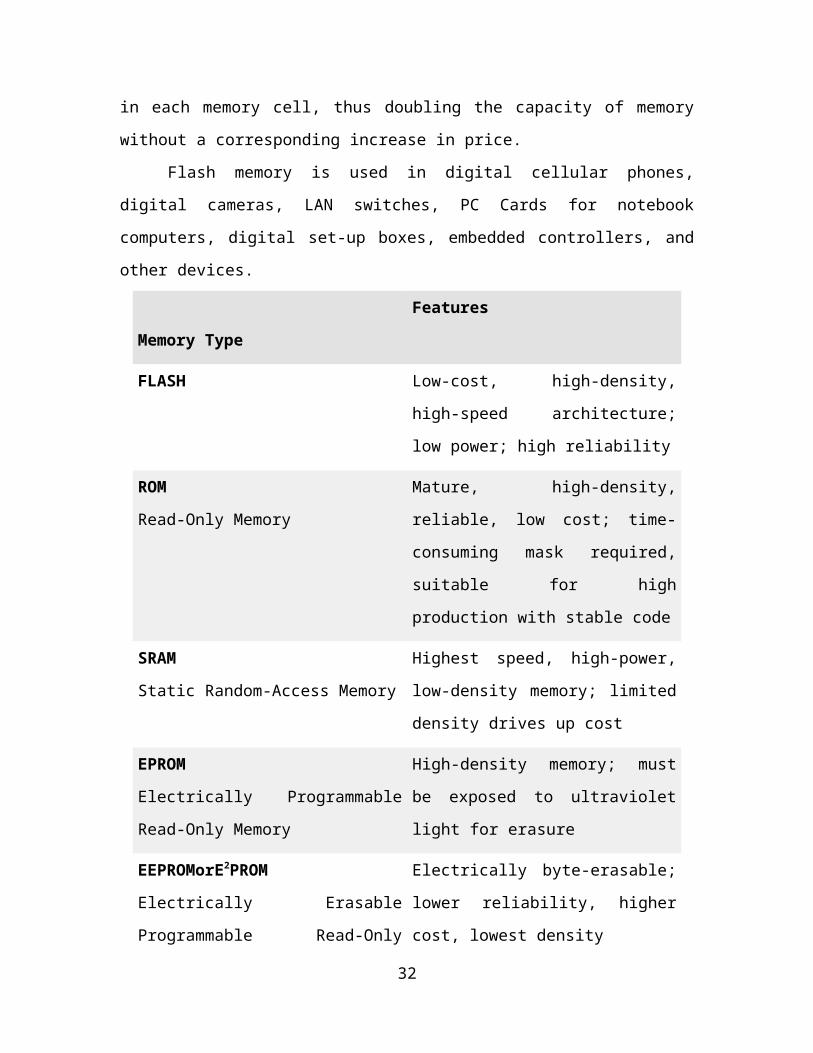
FLASH MEMORY:
Flash memory (sometimes called "flash RAM") is a type of constantly-powered
non volatile that can be erased and reprogrammed in units of memory called blocks. It is
a variation of electrically erasable programmable read-only memory (EEPROM) which,
unlike flash memory, is erased and rewritten at the byte level, which is slower than flash
memory updating. Flash memory is often used to hold control code such as the basic
input/output system (BIOS) in a personal computer. When BIOS needs to be changed
(rewritten), the flash memory can be written to in block (rather than byte) sizes, making it
easy to update. On the other hand, flash memory is not useful as random access memory
(RAM) because RAM needs to be addressable at the byte (not the block) level.
22

Flash memory gets its name because the microchip is organized so that a section
of memory cells are erased in a single action or "flash." The erasure is caused by Fowler-
Nordheim tunneling in which electrons pierce through a thin dielectric material to remove
an electronic charge from a floating gate associated with each memory cell. Intel offers a
form of flash memory that holds two bits (rather than one) in each memory cell, thus
doubling the capacity of memory without a corresponding increase in price.
Flash memory is used in digital cellular phones, digital cameras, LAN switches,
PC Cards for notebook computers, digital set-up boxes, embedded controllers, and other
devices.
Memory Type
Features
FLASH Low-cost, high-density, high-speed
architecture; low power; high reliability
ROM
Read-Only Memory
Mature, high-density, reliable, low cost;
time-consuming mask required, suitable
for high production with stable code
SRAM
Static Random-Access Memory
Highest speed, high-power, low-density
memory; limited density drives up cost
EPROM
Electrically Programmable Read-Only
Memory
High-density memory; must be exposed
to ultraviolet light for erasure
EEPROMorE2PROM
Electrically Erasable Programmable
Read-Only Memory
Electrically byte-erasable; lower
reliability, higher cost, lowest density
DRAM
Dynamic Random Access Memory
High-density, low-cost, high-speed,
high-power
23

Technical Overview of Flash Memory
Flash memory is a nonvolatile memory using NOR technology, which allows the user to
electrically program and erase information. Intel® Flash memory uses memory cells
similar to an EPROM, but with a much thinner, precisely grown oxide between the
floating gate and the source (see Figure 2). Flash programming occurs when electrons are
placed on the floating gate. The charge is stored on the floating gate, with the oxide layer
allowing the cell to be electrically erased through the source. Intel Flash memory is an
extremely reliable nonvolatile memory architecture.
Fig 6: - Pin diagram of AT89C51
24
Pin Description:
VCC: Supply voltage.
GND: Ground.
Port 0:
Port 0 is an 8-bit open-drain bi-directional I/O port. As an output port, each pin
can sink eight TTL inputs. When one’s are written to port 0 pins, the pins can be used as
high impedance inputs. Port 0 may also be configured to be the multiplexed low order
address/data bus during accesses to external program and data memory. In this mode P0
has internal pull-ups. Port 0 also receives the code bytes during Flash programming, and
outputs the code bytes during program verification. External pull-ups are required during
program verification.
Port 1:
Port 1 is an 8-bit bi-directional I/O port with internal pull-ups. The Port 1 output
buffers can sink/source four TTL inputs. When 1s are written to Port 1 pins they are
pulled high by the internal pull-ups and can be used as inputs. As inputs, Port 1 pins that
are externally being pulled low will source current (IIL) because of the internal pull-ups.
Port 1 also receives the low-order address bytes during Flash programming and
verification.
Port 2:
Port 2 is an 8-bit bi-directional I/O port with internal pull-ups. The Port 2 output
buffers can sink/source four TTL inputs. When 1s are written to Port 2 pins they are
pulled high by the internal pull-ups and can be used as inputs. As inputs, Port 2 pins that
are externally being pulled low will source current (IIL) because of the internal pull-ups.
Port 2 emits the high-order address byte during fetches from external program memory
and during accesses to external data memories that use 16-bit addresses (MOVX
@DPTR). In this application, it uses strong internal pull-ups when emitting 1s. During
accesses to external data memories that use 8-bit addresses (MOVX @ RI), Port 2 emits
25
the contents of the P2 Special Function Register. Port 2 also receives the high-order
address bits and some control signals during Flash programming and verification.
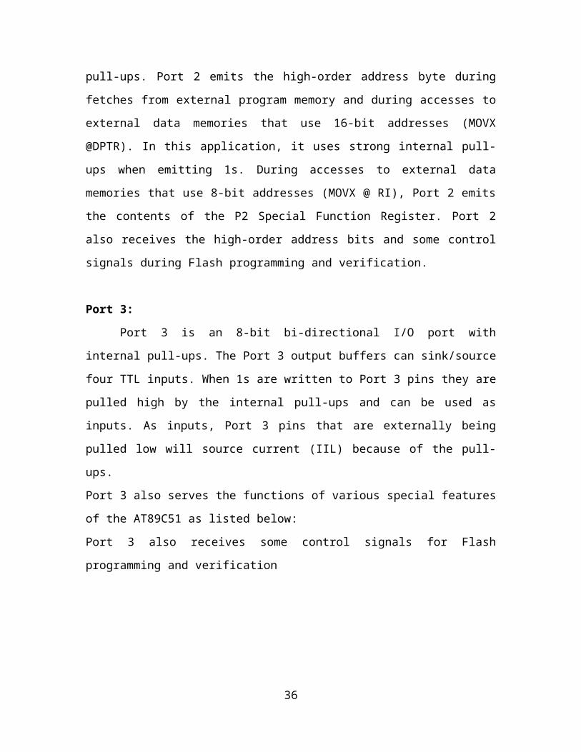
Port 3:
Port 3 is an 8-bit bi-directional I/O port with internal pull-ups. The Port 3 output
buffers can sink/source four TTL inputs. When 1s are written to Port 3 pins they are
pulled high by the internal pull-ups and can be used as inputs. As inputs, Port 3 pins that
are externally being pulled low will source current (IIL) because of the pull-ups.
Port 3 also serves the functions of various special features of the AT89C51 as listed
below:
Port 3 also receives some control signals for Flash programming and verification
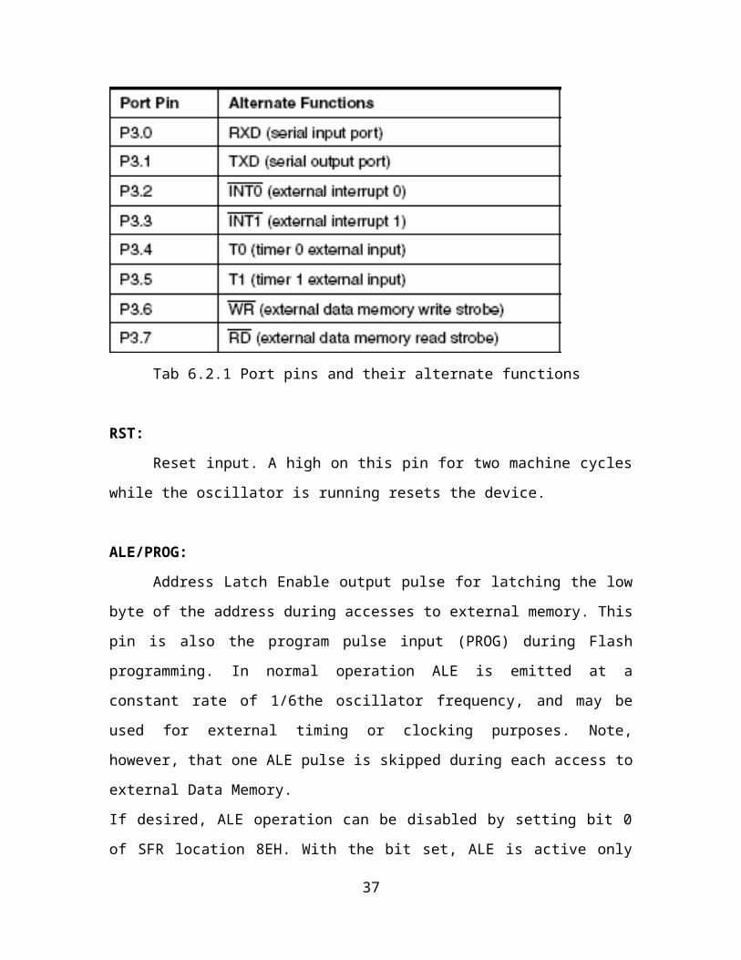
Tab 6.2.1 Port pins and their alternate functions
RST:
Reset input. A high on this pin for two machine cycles while the oscillator is
running resets the device.
ALE/PROG:
Address Latch Enable output pulse for latching the low byte of the address during
accesses to external memory. This pin is also the program pulse input (PROG) during
26

Flash programming. In normal operation ALE is emitted at a constant rate of 1/6the
oscillator frequency, and may be used for external timing or clocking purposes. Note,
however, that one ALE pulse is skipped during each access to external Data Memory.
If desired, ALE operation can be disabled by setting bit 0 of SFR location 8EH. With the
bit set, ALE is active only during a MOVX or MOVC instruction. Otherwise, the pin is
pulled high. Setting the ALE-disable bit has no effect if the microcontroller is in external
execution mode.
PSEN:
Program Store Enable is the read strobe to external program memory. When the
AT89C51 is executing code from external program memory, PSEN is activated twice
each machine cycle, except that two PSEN activations are skipped during each access to
external data memory.
EA/VPP:
External Access Enable EA must be strapped to GND in order to enable the
device to fetch code from external program memory locations starting at 0000H up to
FFFFH.
Note, however, that if lock bit 1 is programmed, EA will be internally latched on
reset.
EA should be strapped to VCC for internal program executions. This pin also receives the
12-volt programming enable voltage (VPP) during Flash programming, for parts that
require 12-volt VPP.
XTAL1:
Input to the inverting oscillator amplifier and input to the internal clock operating
circuit.
XTAL2:
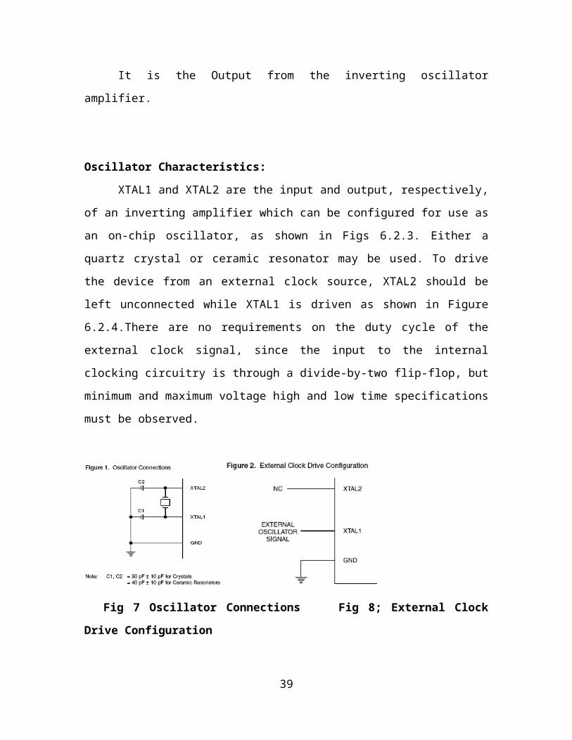
It is the Output from the inverting oscillator amplifier.
27

Oscillator Characteristics:
XTAL1 and XTAL2 are the input and output, respectively, of an inverting
amplifier which can be configured for use as an on-chip oscillator, as shown in Figs
6.2.3. Either a quartz crystal or ceramic resonator may be used. To drive the device from
an external clock source, XTAL2 should be left unconnected while XTAL1 is driven as
shown in Figure 6.2.4.There are no requirements on the duty cycle of the external clock
signal, since the input to the internal clocking circuitry is through a divide-by-two flip-
flop, but minimum and maximum voltage high and low time specifications must be
observed.
Fig 7 Oscillator Connections Fig 8; External Clock Drive Configuration
Notes:
1. Under steady state (non-transient) conditions, IOL must be externally
limited as follows:
Maximum IOL per port pin: 10 mA
Maximum IOL per 8-bit port: Port 0: 26 mA
Ports 1, 2, 3: 15 mA
Maximum total IOL for all output pins: 71 mA
If IOL exceeds the test condition, VOL may exceed the related specification.
Pins are not guaranteed to sink current greater than the listed test conditions.
2. Minimum VCC for Power-down is 2V.
REGISTERS:
28

In the CPU, registers are used to store information temporarily. That information
could be a byte of data to be processed, or an address pointing to the data to be fetched.
The vast majority of 8051 registers are 8–bit registers. In the 8051 there is only one data
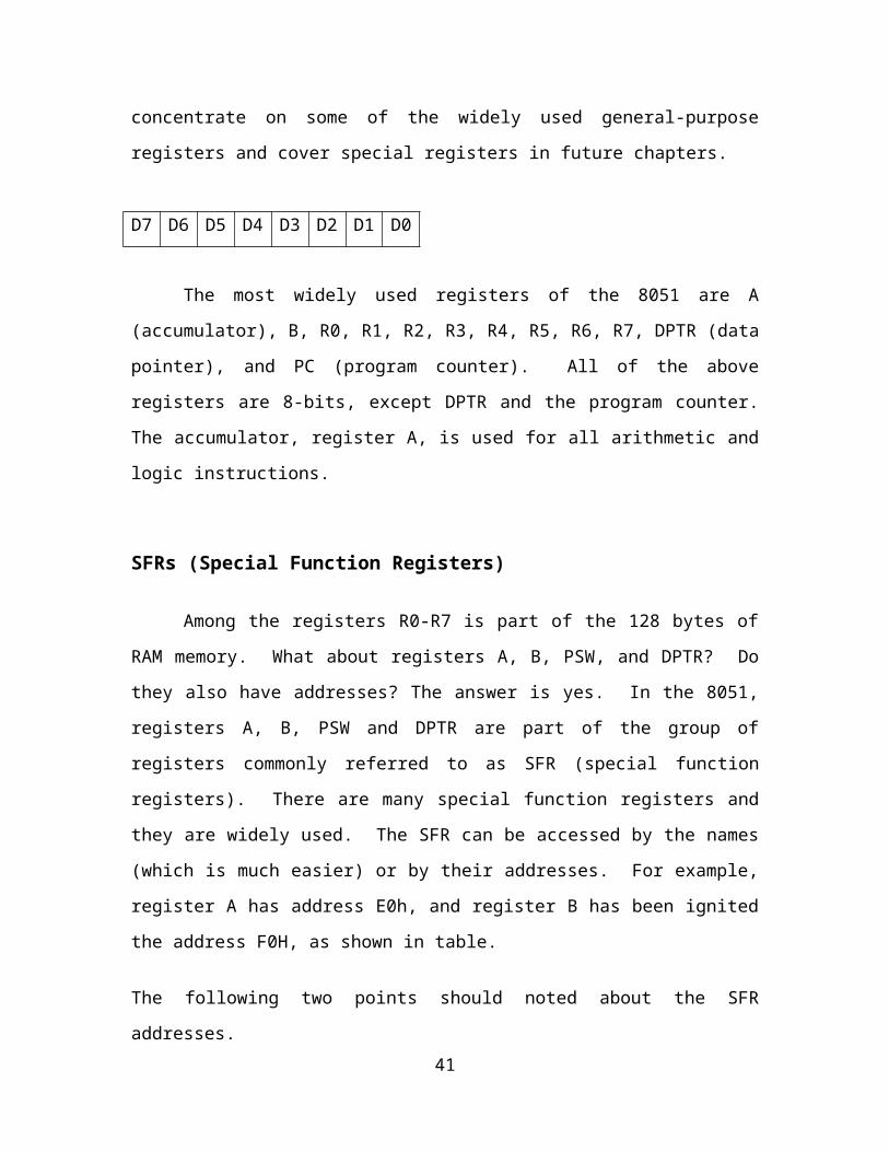
type: 8bits. The 8bits of a register are shown in the diagram from the MSB (most
significant bit) D7 to the LSB (least significant bit) D0. With an 8-bit data type, any data
larger than 8bits must be broken into 8-bit chunks before it is processed. Since there are
a large number of registers in the 8051, we will concentrate on some of the widely used
general-purpose registers and cover special registers in future chapters.
D7 D6 D5 D4 D3 D2 D1 D0
The most widely used registers of the 8051 are A (accumulator), B, R0, R1, R2,
R3, R4, R5, R6, R7, DPTR (data pointer), and PC (program counter). All of the above
registers are 8-bits, except DPTR and the program counter. The accumulator, register A,
is used for all arithmetic and logic instructions.
SFRs (Special Function Registers)
Among the registers R0-R7 is part of the 128 bytes of RAM memory. What about
registers A, B, PSW, and DPTR? Do they also have addresses? The answer is yes. In the
8051, registers A, B, PSW and DPTR are part of the group of registers commonly
referred to as SFR (special function registers). There are many special function registers
and they are widely used. The SFR can be accessed by the names (which is much easier)
or by their addresses. For example, register A has address E0h, and register B has been
ignited the address F0H, as shown in table.
The following two points should noted about the SFR addresses.
1. The Special function registers have addresses between 80H and FFH. These
addresses are above 80H, since the addresses 00 to 7FH are addresses of RAM
memory inside the 8051.
29

2. Not all the address space of 80H to FFH is used by the SFR. The unused
locations 80H to FFH are reserved and must not be used by the 8051
programmer.
Regarding direct addressing mode, notice the following two points: (a) the
address value is limited to one byte, 00-FFH, which means this addressing mode is
limited to accessing RAM locations and registers located inside the 8051. (b) If you
examine the l st file for an assembly language program, you will see that the SFR registers
names are replaced with their addresses as listed in table.
Symbol Name Address
ACC Accumulator 0E0H
B B register 0F0H
PSW Program status word 0D0H
SP Stack pointer 81H
DPTR Data pointer 2 bytes
DPL Low byte 82H
DPH High byte 83H
P0 Port0 80H
P1 Port1 90H
P2 Port2 0A0H
P3 Port3 0B0H
IP Interrupt priority control 0B8H
IE Interrupt enable control 0A8H
TMOD Timer/counter mode control 89H
TCON Timer/counter control 88H
T2CON Timer/counter 2 control 0C8H
T2MOD Timer/counter mode2 control 0C9H
TH0 Timer/counter 0high byte 8CH
TL0 Timer/counter 0 low byte 8AH
TH1 Timer/counter 1 high byte 8DH
30

TL1 Timer/counter 1 low byte 8BH
TH2 Timer/counter 2 high byte 0CDH
TL2 Timer/counter 2 low byte 0CCH
RCAP2H T/C 2 capture register high byte 0CBH
RCAP2L T/C 2 capture register low byte 0CAH
SCON Serial control 98H
SBUF Serial data buffer 99H
PCON Power control 87H
Table: 8051 Special function register Address
A Register (Accumulator)
This is a general-purpose register which serves for storing intermediate results during
operating. A number (an operand) should be added to the accumulator prior to execute an
instruction upon it. Once an arithmetical operation is preformed by the ALU, the result is
placed into the accumulator. If a data should be transferred from one register to another,
it must go through accumulator. For such universal purpose, this is the most commonly
used register that none microcontroller can be imagined without (more than a half 8051
microcontroller's instructions used use the accumulator in some way).
B Register
B register is used during multiply and divide operations which can be performed only
upon numbers stored in the A and B registers. All other instructions in the program can
use this register as a spare accumulator (A).
31
During programming, each of registers is called by name so that their
exact address is not so important for the user. During compiling into machine code (series
of hexadecimal numbers recognized as instructions by the microcontroller), PC will
automatically, instead of registers’ name, write necessary addresses into the
microcontroller.
R Registers (R0-R7)
This is a common name for the total 8 general purpose registers (R0, R1, and R2 ...R7).
Even they are not true SFRs, they deserve to be discussed here because of their purpose.
The bank is active when the R registers it includes are in use. Similar to the accumulator,
they are used for temporary storing variables and intermediate results. Which of the
banks will be active depends on two bits included in the PSW Register. These registers
are stored in four banks in the scope of RAM.
The following example best illustrates the useful purpose of these registers. Suppose that
mathematical operations on numbers previously stored in the R registers should be
performed: (R1+R2) - (R3+R4). Obviously, a register for temporary storing results of
addition is needed. Everything is quite simple and the program is as follows:
32

MOV A, R3; Means: move number from R3 into accumulator
ADD A, R4; Means: add number from R4 to accumulator (result remains in accumulator)
MOV R5, A; Means: temporarily moves the result from accumulator into R5
MOV A, R1; Means: move number from R1 into accumulator
ADD A, R2; Means: add number from R2 to accumulator
SUBB A, R5; Means: subtract number from R5 (there are R3+R4)
8051 Register Banks and Stack
RAM memory space allocation in the 8051
There are 128 bytes of RAM in the 8051. The 128 bytes of RAM inside the
8051 are assigned addresses 00 to7FH. These 128 bytes are divided into three different
groups as follows:
1. A total of 32 bytes from locations 00 to 1FH hex are set aside for register
banks and the stack.
2. A total of 16 bytes from locations 20 to 2FH hex are set aside for bit-
addressable read/write memory.
3. A total of 80 bytes from locations 30H to 7FH are used for read and write
storage, or what is normally called Scratch pad. These 80 locations of RAM
are widely used for the purpose of storing data and parameters nu 8051
programmers.
Register banks in the 8051A total of 32bytes of RAM are set aside for the register banks and stack. These
32 bytes are divided into 4 banks of registers in which each bank has registers, R0-R7.
RAM locations 0 to 7 are set aside for bank 0 of R0-R7 where R0 is RAM location 0, R1
33

is RAM location 1, and R2 is location 2, and so on, until memory location7, which
belongs to R7 of bank0. The second bank of registers R0-R7 starts at RAM location 08
and goes to location 0FH. The third bank of R0-R7 starts at memory location 10H and
goes to location 17H. Finally, RAM locations 18H to 1FH are set aside for the fourth
bank of R0-R7. Fig shows how the 32 bytes are allocated into 4 banks.
As we can see from fig 1, the bank 1 uses the same RAM space as the stack.
This is a major problem in programming the 8051. we must either not use register bank1,
or allocate another area of RAM for the stack.
Default register bankIf RAM locations 00-1F are set aside for the four register banks, which register
bank of R0-R7 do we have access to when the 8051 is powered up? The answer is
register bank 0; that is , RAM locations 0, 1,2,3,4,5,6, and 7 are accessed with the names
R0, R1, R2, R3, R4, R5, R6, and R7 when programming the 8051. It is much easier to
refer to these RAM locations with names such as R0, R1 and so on, than by their memory
locations as shown in fig 2.
The register banks are switched by using the D3 & D4 bits of register PSW.
Fig 9: RAM Allocation in the 8051
34

Fig 10: 8051 Register Banks and their RAM Addresses
PSW Register (Program Status Word)
This is one of the most important SFRs. The Program Status Word (PSW) contains
several status bits that reflect the current state of the CPU. This register contains: Carry
bit, Auxiliary Carry, two register bank select bits, Overflow flag, parity bit, and user-
definable status flag. The ALU automatically changes some of register’s bits, which is
usually used in regulation of the program performing.
P - Parity bit. If a number in accumulator is even then this bit will be automatically set
(1), otherwise it will be cleared (0). It is mainly used during data transmission and
receiving via serial communication.
35
- Bit 1. This bit is intended for the future versions of the microcontrollers, so it is not
supposed to be here.
OV Overflow occurs when the result of arithmetical operation is greater than 255
(decimal), so that it can not be stored in one register. In that case, this bit will be set (1).
If there is no overflow, this bit will be cleared (0).
RS0, RS1 - Register bank selects bits. These two bits are used to select one of the four
register banks in RAM. By writing zeroes and ones to these bits, a group of registers R0-
R7 is stored in one of four banks in RAM.
RS1 RS2 Space in RAM
0 0 Bank0 00h-07h
0 1 Bank1 08h-0Fh
1 0 Bank2 10h-17h
1 1 Bank3 18h-1Fh
F0 - Flag 0. This is a general-purpose bit available to the user.
AC - Auxiliary Carry Flag is used for BCD operations only.
CY - Carry Flag is the (ninth) auxiliary bit used for all arithmetical operations and shift
instructions.
DPTR Register (Data Pointer)
These registers are not true ones because they do not physically exist. They consist of two
separate registers: DPH (Data Pointer High) and (Data Pointer Low). Their 16 bits are
used for external memory addressing. They may be handled as a 16-bit register or as two
independent 8-bit registers. Besides, the DPTR Register is usually used for storing data
and intermediate results which have nothing to do with memory locations.
36
SP Register (Stack Pointer)
The stack is a section of RAM used by the CPU to store information
temporarily. This information could be data or an address. The CPU needs this storage
area since there are only a limited number of registers.
How stacks are accessed in the 8051
If the stack is a section of RAM, there must be registers inside the CPU to point
to it. The register used to access the stack is called the SP (Stack point) Register. The
stack pointer in the 8051 is only 8 bits wide; which means that it can take values of 00 to
FFH. When the 8051 is powered up, the SP register contains value 07. This means that
RAM location 08 is the first location used for the stack by the 8051. The storing of a
CPU register in the stack is called a PUSH, and pulling the contents off the stack back
into a CPU register is called a POP. In other words, a register is pushed onto the stack to
save it and popped off the stack to retrieve it. The job of the SP is very critical when
push and pop actions are performed.
37

Pushing onto the stack
In the 8051 the stack pointer (SP) points to the last used location of the stack. As
we push data onto the stack, the stack pointer is incremented by one. Notice that this
different from many microprocessors, notably x86 processors in which the SP is
decremented when data is pushed onto the stack. As each PUSH is executed, the
contents of the register are saved on the stack and SP is incremented by 1. Notice that for
every byte of data saved on the stack and then SP is incremented only once. Notice also
that to push the registers onto the stack we must use their RAM addresses. For example,
the instruction “PUSH” pushes register R1 onto the stack.
Popping from the stack
Popping the contents of the stack back into a given register is the opposite process
of pushing. With every pop, the top byte of the stack is copied to the register specified by
the instruction and the stack pointer is decremented once.
The upper limit of the stack
As, mentioned earlier, locations 08 to 1FH in the 8051 RAM can be used for the
stack. This is because locations 20-2FH of RAM are reserved for bit-addressable
memory and must not be used by the stack. If in a program we need more than 24 bytes
(08 to 1FH=24bytes) of stack, we can change the SP to point to RAM locations 30-7FH.
This is done with the instruction “MOV SP, #XX”.
P0, P1, P2, P3 - Input/Output Registers
In case that external memory and serial communication system are not in use then, 4
ports with in total of 32 input-output lines are available to the user for connection to
peripheral environment. Each bit inside these ports corresponds to the appropriate pin on
38
the microcontroller. This means that logic state written to these ports appears as a voltage
on the pin (0 or 5 V). Naturally, while reading, the opposite occurs – voltage on some
input pins is reflected in the appropriate port bit.
The state of a port bit, besides being reflected in the pin, determines at the same time
whether it will be configured as input or output. If a bit is cleared (0), the pin will be
configured as output. In the same manner, if a bit is set to 1 the pin will be configured as
input. After reset, as well as when turning the microcontroller ON, all bits on these ports
are set to one (1). This means that the appropriate pins will be configured as inputs.
Program counter:
The important register in the 8051 is the PC (Program counter). The program
counter points to the address of the next instruction to be executed. As the CPU fetches
the OPCODE from the program ROM, the program counter is incremented to point to the
next instruction. The program counter in the 8051 is 16bits wide. This means that the
8051 can access program addresses 0000 to FFFFH, a total of 64k bytes of code.
However, not all members of the 8051 have the entire 64K bytes of on-chip ROM
installed, as we will see soon.
Types of instructions
Depending on operation they perform, all instructions are divided in several groups:
Arithmetic Instructions
Branch Instructions
Data Transfer Instructions
Logical Instructions
Logical Instructions with bits
The first part of each instruction, called MNEMONIC refers to the operation an
instruction performs (copying, addition, logical operation etc.). Mnemonics commonly
are shortened form of name of operation being executed. For example:
39

INC R1; Increment R1 (increment register R1)
LJMP LAB5 ;Long Jump LAB5 (long jump to address specified as LAB5)
JNZ LOOP ;Jump if Not Zero LOOP (if the number in the accumulator is not 0, jump to
address specified as LOOP)
Another part of instruction, called OPERAND is separated from mnemonic at least by
one empty space and defines data being processed by instructions. Some instructions
have no operand; some have one, two or three. If there is more than one operand in
instruction, they are separated by comma. For example:
RET - (return from sub-routine)
JZ TEMP - (if the number in the accumulator is not 0, jump to address specified as TEMP)
ADD A,R3 - (add R3 and accumulator)
CJNE A,#20,LOOP - (compare accumulator with 20. If they are not equal, jump to address
specified as LOOP)
Arithmetic instructions These instructions perform several basic operations (addition,
subtraction, division, multiplication etc.) After execution, the result is stored in the first
operand. For example:
ADD A, R1 - The result of addition (A+R1) will be stored in the accumulator.
Arithmetical Instructions
Mnemonic DescriptionByte
Number
Oscillator
Period
ADD A,Rn Add R Register to accumulator 1 1
ADD A,RxAdd directly addressed Rx Register to
accumulator2 2
ADD A,@RiAdd indirectly addressed Register to
accumulator1 1
ADD A,#X Add number X to accumulator 2 2
40
ADDC A,Rn Add R Register with Carry bit to accumulator 1 1
Branch Instructions
There are two kinds of these instructions:
Unconditional jump instructions: After their execution a jump to a new location from
where the program continues execution is executed.
Conditional jump instructions: If some condition is met - a jump is executed.
Otherwise, the program normally proceeds with the next instruction.
Branch Instruction
Mnemonic DescriptionByte
Number
Oscillator
Period
ACALL
adr11
Call subroutine located at address within 2 K
byte Program Memory space2 3
LCALL
adr16
Call subroutine located at any address within
64 K byte Program Memory space3 4
RET Return from subroutine 1 4
RETI Return from interrupt routine 1 4
AJMP adr11Jump to address located within 2 K byte
Program Memory space2 3
LJMP adr16Jump to any address located within 64 K byte
Program Memory space3 4
41

Data Transfer Instructions
These instructions move the content of one register to another one. The register which
content is moved remains unchanged. If they have the suffix “X” (MOVX), the data is
exchanged with external memory.
Data Transfer Instruction
Mnemonic DescriptionByte
Number
Cycle
Number
MOV A,Rn Move R register to accumulator 1 1
MOV A,RxMove directly addressed Rx register to
accumulator2 2
MOV A,@RiMove indirectly addressed register to
accumulator1 1
MOV A,#X Move number X to accumulator 2 2
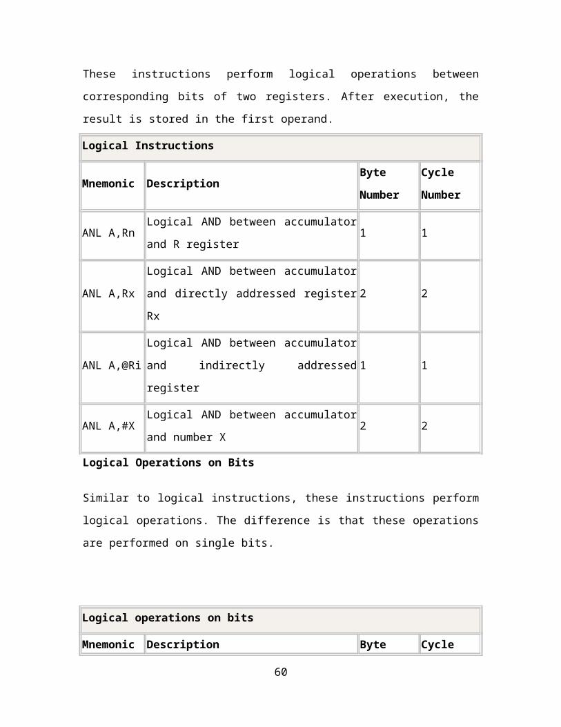
Logical Instructions
These instructions perform logical operations between corresponding bits of two
registers. After execution, the result is stored in the first operand.
Logical Instructions
Mnemonic DescriptionByte
Number
Cycle
Number
ANL A,RnLogical AND between accumulator and R
register1 1
ANL A,RxLogical AND between accumulator and
directly addressed register Rx2 2
ANL A,@Ri Logical AND between accumulator and 1 1
42

indirectly addressed register
ANL A,#XLogical AND between accumulator and
number X2 2
Logical Operations on Bits
Similar to logical instructions, these instructions perform logical operations. The
difference is that these operations are performed on single bits.
Logical operations on bits
Mnemonic DescriptionByte
Number
Cycle
Number
CLR C Clear Carry bit 1 1
CLR bit Clear directly addressed bit 2 2
SETB C Set Carry bit 1 1
SETB bit Set directly addressed bit 2 2
CPL C Complement Carry bit 1 1
CPL bit Complement directly addressed bit 2 2
TIMERSOn-chip timing/counting facility has proved the capabilities of the microcontroller
for implementing the real time application. These includes pulse counting, frequency
measurement, pulse width measurement, baud rate generation, etc,. Having sufficient
number of timer/counters may be a need in a certain design application. The 8051 has
two timers/counters. They can be used either as timers to generate a time delay or as
counters to count events happening outside the microcontroller. Let discuss how these
43

timers are used to generate time delays and we will also discuss how they are been used
as event counters.
PROGRAMMING 8051 TIMERS
The 8051 has timers: Timer 0 and Timer1.they can be used either as timers or as
event counters. Let us first discuss about the timers’ registers and how to program the
timers to generate time delays.
BASIC RIGISTERS OF THE TIMER
Both Timer 0 and Timer 1 are 16 bits wide. Since the 8051 has an 8-bit
architecture, each 16-bit timer is accessed as two separate registers of low byte and high
byte.
TIMER 0 REGISTERS
The 16-bit register of Timer 0 is accessed as low byte and high byte. the low
byte register is called TL0(Timer 0 low byte)and the high byte register is referred to as
TH0(Timer 0 high byte).These register can be accessed like any other register, such as
A,B,R0,R1,R2,etc.for example, the instruction ”MOV TL0, #4F”moves the value 4FH
into TL0,the low byte of Timer 0.These registers can also be read like any other register.
44

TIMER 1 REGISTERS
Timer 1 is also 16-bit register is split into two bytes, referred to as TL1 (Timer
1 low byte) and TH1 (Timer 1 high byte).these registers are accessible n the same way as
the register of Timer 0.
TMOD (timer mode) REGISTER
Both timers TIMER 0 and TIMER 1 use the same register, called TMOD, to set
the various timer operation modes. TMOD is an 8-bit register in which the lower 4 bits
are set aside for Timer 0 and the upper 4 bits for Timer 1.in each case; the lower 2 bits
are used to set the timer mode and the upper 2 bits to specify the operation.
45

MODES:
M1, M0:
M0 and M1 are used to select the timer mode. There are three modes: 0, 1,
2.Mode 0 is a 13-bit timer, mode 1 is a 16-bit timer, and mode 2 is an 8-bit timer. We will
concentrate on modes 1 and 2 since they are the ones used most widely. We will soon
describe the characteristics of these modes, after describing the reset of the TMOD
register.
GATE Gate control when set. The timer/counter is enabled only
While the INTx pin is high and the TRx control pin is.
Set. When cleared, the timer is enabled.
C/T Timer or counter selected cleared for timer operation
(Input from internal system clock).set for counter
O Operation (input TX input pin).
M 1 Mode bit 1
M0 Mode bit 0
M1 M0 MODE Operating Mode
0 0 0 13-bit timer mode
8-bit timer/counter THx with TLx as
5 - Bit pre-scaler.
0 1 1 16-bit timer mode
16-bit timer/counters THx with TLx are
Cascaded; there is no prescaler
1 0 2 8-bit auto reload
8-bit auto reload timer/counter;THx
Holds a value that is to be reloaded into
TLx each time it overflows.
46

1 1 3 Split timer mode.
C/T (clock/timer)
This bit in the TMOD register is used to decide whether the timer is used as a delay
generator or an event counter. If C/T=0, it is used as a timer for time delay generation.
The clock source for the time delay is the crystal frequency of the 8051.this section is
concerned with this choice. The timer’s use as an event counter is discussed in the next
section.
Serial Communication:Computers can transfer data in two ways: parallel and serial. In parallel data
transfers, often 8 or more lines (wire conductors) are used to transfer data to a device that
is only a few feet away. Examples of parallel data transfer are printers and hard disks;
each uses cables with many wire strips. Although in such cases a lot of data can be
transferred in a short amount of time by using many wires in parallel, the distance cannot
be great. To transfer to a device located many meters away, the serial method is used. In
serial communication, the data is sent one bit at a time, in contrast to parallel
communication, in which the data is sent a byte or more at a time. Serial communication
of the 8051 is the topic of this chapter. The 8051 has serial communication capability
built into it, there by making possible fast data transfer using only a few wires.
If data is to be transferred on the telephone line, it must be converted from 0s
and 1s to audio tones, which are sinusoidal-shaped signals. A peripheral device called a
modem, which stands for “modulator/demodulator”, performs this conversion.
Serial data communication uses two methods, asynchronous and synchronous.
The synchronous method transfers a block of data at a time, while the asynchronous
method transfers a single byte at a time.
In data transmission if the data can be transmitted and received, it is a duplex
transmission. This is in contrast to simplex transmissions such as with printers, in which
the computer only sends data. Duplex transmissions can be half or full duplex,
depending on whether or not the data transfer can be simultaneous. If data is transmitted
47

one way at a time, it is referred to as half duplex. If the data can go both ways at the
same time, it is full duplex. Of course, full duplex requires two wire conductors for the
data lines, one for transmission and one for reception, in order to transfer and receive data
simultaneously.
Asynchronous serial communication and data framing
The data coming in at the receiving end of the data line in a serial data transfer
is all 0s and 1s; it is difficult to make sense of the data unless the sender and receiver
agree on a set of rules, a protocol, on how the data is packed, how many bits constitute a
character, and when the data begins and ends.
Start and stop bits
Asynchronous serial data communication is widely used for character-oriented
transmissions, while block-oriented data transfers use the synchronous method. In the
asynchronous method, each character is placed between start and stop bits. This is called
framing. In the data framing for asynchronous communications, the data, such as ASCII
characters, are packed between a start bit and a stop bit. The start bit is always one bit,
but the stop bit can be one or two bits. The start bit is always a 0 (low) and the stop bit
(s) is 1 (high).
Data transfer rate
The rate of data transfer in serial data communication is stated in bps (bits per
second). Another widely used terminology for bps is baud rate. However, the baud and
bps rates are not necessarily equal. This is due to the fact that baud rate is the modem
terminology and is defined as the number of signal changes per second. In modems a
single change of signal, sometimes transfers several bits of data. As far as the conductor
wire is concerned, the baud rate and bps are the same, and for this reason we use the bps
and baud interchangeably.
The data transfer rate of given computer system depends on communication
ports incorporated into that system. For example, the early IBMPC/XT could transfer
data at the rate of 100 to 9600 bps. In recent years, however, Pentium based PCS transfer
data at rates as high as 56K bps. It must be noted that in asynchronous serial data
communication, the baud rate is generally limited to 100,000bps.
48

RS232 Standards
To allow compatibility among data communication equipment made by various
manufacturers, an interfacing standard called RS232 was set by the Electronics Industries
Association (EIA) in 1960. In 1963 it was modified and called RS232A. RS232B AND
RS232C were issued in 1965 and 1969, respectively. Today, RS232 is the most widely
used serial I/O interfacing standard. This standard is used in PCs and numerous types of
equipment. However, since the standard was set long before the advert of the TTL logic
family, its input and output voltage levels are not TTL compatible. In RS232, a 1 is
represented by -3 to -25V, while a 0 bit is +3 to +25V, making -3 to +3 undefined. For
this reason, to connect any RS232 to a microcontroller system we must use voltage
converters such as MAX232 to convert the TTL logic levels to the RS232 voltage levels,
and vice versa. MAX232 IC chips are commonly referred to as line drivers.
RS232 pins
RS232 cable is commonly referred to as the DB-25 connector. In labeling, DB-
25P refers to the plug connector (male) and DB-25S is for the socket connector (female).
Since not all the pins are used in PC cables, IBM introduced the DB-9 Version of the
serial I/O standard, which uses 9 pins only, as shown in table.
DB-9 pin connector
1 2 3 4 5
6 7 8 9
(Out of computer and exposed end of cable)
Pin Functions:
Pin Description
1 Data carrier detect (DCD)
2 Received data (RXD)
3 Transmitted data (TXD)
4 Data terminal ready(DTR)
49

5 Signal ground (GND)
6 Data set ready (DSR)
7 Request to send (RTS)
8 Clear to send (CTS)
9 Ring indicator (RI)
Note: DCD, DSR, RTS and CTS are active low pins.
The method used by RS-232 for communication allows for a simple connection of three
lines: Tx, Rx, and Ground. The three essential signals for 2-way RS-232
Communications are these:
TXD: carries data from DTE to the DCE.
RXD: carries data from DCE to the DTE
SG: signal ground
8051 connection to RS232The RS232 standard is not TTL compatible; therefore, it requires a line driver
such as the MAX232 chip to convert RS232 voltage levels to TTL levels, and vice versa.
The interfacing of 8051 with RS232 connectors via the MAX232 chip is the main topic.
The 8051 has two pins that are used specifically for transferring and
receiving data serially. These two pins are called TXD and RXD and a part of the port 3
group (P3.0 and P3.1). Pin 11 of the 8051 is assigned to TXD and pin 10 is designated as
RXD. These pins are TTL compatible; therefore, they require a line driver to make them
RS232 compatible. One such line driver is the MAX232 chip.
MAX232 converts from RS232 voltage levels to TTL voltage
levels, and vice versa. One advantage of the MAX232 chip is that it uses a +5V power
source which, is the same as the source voltage for the 8051. In the other words, with a
single +5V power supply we can power both the 8051 and MAX232, with no need for the
power supplies that are common in many older systems. The MAX232 has two sets of
50

line drivers for transferring and receiving data. The line drivers used for TXD are called
T1 and T2, while the line drivers for RXD are designated as R1 and R2. In many
applications only one of each is used.
CONNECTING μC to PC using MAX 232
INTERRUPTSA single microcontroller can serve several devices. There are two ways to do that:
INTERRUPTS or POLLING.
POLLING:
In polling the microcontroller continuously monitors the status of a given device; when
the status condition is met, it performs the service .After that, it moves on to monitor the
next device until each one is serviced. Although polling can monitor the status of several
devices and serve each of them as certain condition are met.
INTERRUPTS:
In the interrupts method, whenever any device needs its service, the device notifies
the microcontroller by sending it an interrupts signal. Upon receiving an interrupt signal,
the microcontroller interrupts whatever it is doing and serves the device. The program
associated with the interrupts is called the interrupt service routine (ISR).or interrupt
handler.
INTERRUPTS Vs POLLING:
The advantage of interrupts is that the microcontroller can serve many devices (not all the
same time, of course); each device can get the attention of the microcontroller based on
51

the priority assigned to it. The polling method cannot assign priority since it checks all
devices in round-robin fashion. More importantly, in the interrupt method the
microcontroller can also ignore (mask) a device request for service. This is again not
possible with the polling method. The most important reason that the interrupt method is
preferable is that the polling method wastes much of the microcontroller’s time by
polling devices that do not need service. So, in order to avoid tying down the
microcontroller, interrupts are used.
INTERRUPT SERVICE ROUTINE
For every interrupt, there must be an interrupt service routine (ISR), or interrupt handler.
When an interrupt is invoked, the microcontroller runs the interrupts service routine. For
every interrupt, there is a fixed location in memory that holds the address of its ISR. The
group of memory location set aside to hold the addresses of ISR and is called the
Interrupt Vector Table. Shown below:
Interrupt Vector Table for the 8051:
S.No. INTERRUPT ROM LOCATION
(HEX)
PIN FLAG
CLEARING
1. Reset 0000 9 Auto
2. External
hardware
Interrupt 0
0003 P3.2 (12) Auto
3. Timers 0 interrupt (TF0)
000B Auto
4. External
hardware
0013 P3.3 (13) Auto
52

Interrupt
1(INT1)
5. Timers 1 interrupt (TF1)
001B Auto
6. Serial COM (RI and TI)
0023 Programmer clears it
Six Interrupts in the 8051:
In reality, only five interrupts are available to the user in the 8051, but many
manufacturers’ data sheets state that there are six interrupts since they include reset .the
six interrupts in the 8051 are allocated as above.
1. Reset. When the reset pin is activated, the 8051 jumps to address location
0000.this is the power-up reset.
2. Two interrupts are set aside for the timers: one for Timer 0 and one for Timer
1.Memory location 000BH and 001BH in the interrupt vector table belong to
Timer 0 and Timer 1, respectively.
3. Two interrupts are set aside for hardware external harder interrupts. Pin number
12(P3.2) and 13(P3.3) in port 3 are for the external hardware interrupts INT0 and
INT1,respectively.These external interrupts are also referred to as EX1 and
EX2.Memory location 0003H and 0013H in the interrupt vector table are
assigned to INT0 and INT1, respectively.
4. Serial communication has a single interrupt that belongs to both receive and
transmit. The interrupt vector table location 0023H belongs to this interrupt.
Notice that a limited number of bytes are set aside for each interrupt. For example, a total
of 8 bytes from location 0003 to 000A is set aside for INT0, external hardware interrupt
0.similarly,a total of 8 bytes from location 00BH to 0012H is reserved for TF0, Timer 0
interrupt. If the service routine for a given interrupt is short enough to fit in the memory
space allocated to it, it is placed in the vector table; otherwise, and an LJMP instruction is
53

placed in the vector table to point to the address of the ISR. In that rest of the bytes
allocated to that interrupt are unused.
From the above table also notice that only three bytes of ROM space are assigned to the
reset pin. they are ROM address location 0,1 and2.address location 3 belongs to external
hardware interrupt 0.for this reason, in our program we put the LJMP as the first
instruction and redirect the processor away from the interrupt vector table, as shown
below
Steps in executing an interrupt
Upon activation of an interrupt, the microcontroller goes through the following steps.
1. It finishes the instruction it is executing and saves the address of the next
instruction (PC) on the stack.
2. It also saves the current status of all the interrupts internally (i.e., not on the
stack).
3. It jumps to a fixed location in memory called the interrupt vector table that holds
the address of the interrupts service routine.
4. The microcontroller gets the address of the ISR from the interrupt vector table and
jumps to it. It starts to execute the interrupt service subroutine until it reaches the
last instruction of the subroutine, which is RETI (return from interrupt).
5. Upon executing the RETI instruction, the microcontroller returns to the place
where it was interrupted. First, it gets the program counter (PC) address from the
stack by popping the top two bytes of the stack into the PC. Then it starts to
execute from that address.
Notice from step 5 the critical role of the stack. For this reason, we must be careful in
manipulating the stack contents in the ISR. Specifically, in the ISR, just as in any CALL
subroutine, the number of pushes and pops must be equal.
Enabling and disabling an interrupt:
54

Upon reset, all interrupt are disabled (masked), meaning that none will be responded to
by the microcontroller if they are activated. The interrupt must be enabled by software in
order for the microcontroller to respond to them. There is a register called IE (interrupt
enable) that is responsible for enabling (unmasking) and disabling (masking) the
interrupts.
Notice that IE is a bit-addressable register.
Steps in enabling an interrupt:
To enable an interrupt, we take the following steps:
1. Bit D7 of the IE register (EA) must be set to high to allow the reset to take effect.
If EA=1, interrupts are enabled and will be responded to if their corresponding bit in IE
are high. If EA=0, no interrupt will be responded to, even if the associated bit in the IE
register is high.
Interrupt Enable Register
D7 D6 D5 D4 D3 D2 D1 D0
EA IE.7 disables all interrupts. If EA=0, no interrupts is acknowledged.
If EA=1, each interrupt source is individually enabled disabled
By setting or clearing its enable bit.
-- IE.6 Not implemented, reserved for future use.*
ET2 IE.5 Enables or disables Timer 2 overflow or capture interrupt (8052
Only)
ES IE.4 Enables or disables the serial port interrupts.
ET1 IE.3 Enables or disables Timers 1 overflow interrupt
55
EA -- ET2 ES ET1 EX1 ET0 EX0

EX1 IE.2 Enables or disables external interrupt 1.
ET0 IE.1 Enables or disables Timer 0 overflow interrupt.
EX0 IE.0 Enables or disables external interrupt.
5.3 FIRE SENSOR (ST-1KL3B)
The ST-1KL3A and 1KL3B are high-sensitivity NPN silicon phototransistors
mounted in durable, hermetically sealed TO-18 metal can which provide years of reliable
performance, even under demanding conditions such as use outdoors.
FEATURES:
•Narrow angular response
•Durable
•High reliability in demanding environments
•Two leads (Collector, Emitter) ST-1KL3A
•Three leads (Collector, Emitter, Base) ST-1 K L 3 B
APPLICATIONS:
•Optical switches
•Optical detectors
•Infrared sensors
•Encoders
•Smoke detectors
56

57

6. SERIAL COMMUNICATION
58

Computers can transfer data in two ways: parallel and serial. In parallel data transfers,
often 8 or more lines (wire conductors) are used to transfer data to a device that is only a few
feet away. Examples of parallel data transfer are printers and hard disks; each uses cables with
many wire strips. Although in such cases a lot of data can be transferred in a short amount of
time by using many wires in parallel, the distance cannot be great. To transfer to a device
located many meters away, the serial method is used. In serial communication, the data is sent
one bit at a time, in contrast to parallel communication, in which the data is sent a byte or more
at a time. Serial communication of the 8051 is the topic of this chapter. The 8051 has serial
communication capability built into it, there by making possible fast data transfer using only a
few wires.
If data is to be transferred on the telephone line, it must be converted from 0s and 1s
to audio tones, which are sinusoidal-shaped signals. A peripheral device called a modem,
which stands for “modulator/demodulator”, performs this conversion.
Serial data communication uses two methods, asynchronous and synchronous. The
synchronous method transfers a block of data at a time, while the asynchronous method
transfers a single byte at a time.
In data transmission if the data can be transmitted and received, it is a duplex
transmission. This is in contrast to simplex transmissions such as with printers, in which the
computer only sends data. Duplex transmissions can be half or full duplex, depending on
whether or not the data transfer can be simultaneous. If data is transmitted one way at a time, it
is referred to as half duplex. If the data can go both ways at the same time, it is full duplex. Of
course, full duplex requires two wire conductors for the data lines, one for transmission and
one for reception, in order to transfer and receive data simultaneously.
Asynchronous serial communication and data framing
The data coming in at the receiving end of the data line in a serial data transfer is all
0s and 1s; it is difficult to make sense of the data unless the sender and receiver agree on a set
of rules, a protocol, on how the data is packed, how many bits constitute a character, and when
the data begins and ends.
59
Start and stop bits
Asynchronous serial data communication is widely used for character-oriented
transmissions, while block-oriented data transfers use the synchronous method. In the
asynchronous method, each character is placed between start and stop bits. This is called
framing. In the data framing for asynchronous communications, the data, such as ASCII
characters, are packed between a start bit and a stop bit. The start bit is always one bit, but the
stop bit can be one or two bits. The start bit is always a 0 (low) and the stop bit (s) is 1 (high).
Data transfer rate
The rate of data transfer in serial data communication is stated in bps (bits per
second). Another widely used terminology for bps is baud rate. However, the baud and bps
rates are not necessarily equal. This is due to the fact that baud rate is the modem terminology
and is defined as the number of signal changes per second. In modems a single change of
signal, sometimes transfers several bits of data. As far as the conductor wire is concerned, the
baud rate and bps are the same, and for this reason we use the bps and baud interchangeably.
The data transfer rate of given computer system depends on communication ports
incorporated into that system. For example, the early IBMPC/XT could transfer data at the rate
of 100 to 9600 bps. In recent years, however, Pentium based PCS transfer data at rates as high
as 56K bps. It must be noted that in asynchronous serial data communication, the baud rate is
generally limited to 100,000bps.
Computers can transfer data in two ways: parallel and serial. In parallel data transfers,
often 8 or more lines (wire conductors) are used to transfer data to a device that is only a few
feet away. Examples of parallel transfers are printers and hard disks; each uses cables with
many wire strips. Although in such cases a lot of data can be transferred in a short amount of
time by using many wires in parallel, the distance cannot be great. To transfer to a device
located many meters away, the serial method is used. In serial communication, the data is sent
one bit at a time, in contrast to parallel communication, in which the data is sent a byte or more
at a time. The 8051 has serial communication capability built into it, there by making possible
fast data transfer using only a few wires. The PC uses RS 232 as a Serial Communication
Standard.
60

RS232 Standards
To allow compatibility among data communication equipment made by various
manufacturers, an interfacing standard called RS232 was set by the Electronics Industries
Association (EIA) in 1960. In 1963 it was modified and called RS232A. RS232B AND
RS232C were issued in 1965 and 1969, respectively. Today, RS232 is the most widely used
serial I/O interfacing standard. This standard is used in PCs and numerous types of equipment.
However, since the standard was set long before the advert of the TTL logic family, its input
and output voltage levels are not TTL compatible. In RS232, a 1 is represented by -3 to -25V,
while a 0 bit is +3 to +25V, making -3 to +3 undefined. For this reason, to connect any RS232
to a microcontroller system we must use voltage converters such as MAX232 to convert the
TTL logic levels to the RS232 voltage levels, and vice versa. MAX232 IC chips are
commonly referred to as line drivers.
RS232 pins
RS232 cable connector commonly referred to as the DB-25 connector. In labeling, DB-
25P refers to the plug connector (male) and DB-25S is for the socket connector (female).
Since not all the pins are used in PC cables, IBM introduced the DB-9 Version of the serial
I/O standard, which uses 9 pins only, as shown in table.
DB-9 pin connector
1 2 3 4 5
6 7 8 9
(Out of computer and exposed end of cable)
Pin Functions:
Pin Description
1 Data carrier detect (DCD)
2 Received data (RXD)
3 Transmitted data (TXD)
4 Data terminal ready(DTR)
61

5 Signal ground (GND)
6 Data set ready (DSR)
7 Request to send (RTS)
8 Clear to send (CTS)
9 Ring indicator (RI)
Note: DCD, DSR, RTS and CTS are active low pins.
The method used by RS-232 for communication allows for a simple connection of three lines
namely Tx, Rx, and Ground.
TXD: carries data from DTE to the DCE.
RXD: carries data from DCE to the DTE
SG: signal ground
8051 connection to RS232:
The RS232 standard is not TTL compatible; therefore, it requires a Line Driver such as
the MAX232 chip to convert RS232 voltage levels to TTL levels, and vice versa.
The 8051 has two pins that are used specifically for transferring and receiving data
serially. These two pins are TXD and RXD and are a part of the port 3 (P3.0 and P3.1). Pin 11
of the 8051 is designated as TXD and pin 10 as RXD. These pins are TTL compatible;
therefore, they require a line driver to make them RS232 compatible. One such line driver is
the MAX232 chip.
62

MAX232 converts from RS232 voltage levels to TTL voltage levels, and vice versa.
One advantage of the MAX232 chip is that it uses a +5V power source which, is the same as
the source voltage for the 8051. In the other words, with a single +5V power supply we can
power both the 8051 and MAX232, with no need for the power supplies. The MAX232 has
two sets of line drivers for transferring and receiving data. The line drivers used for TXD are
called T1 and T2, while the line drivers for RXD are designated as R1 and R2. In many
applications only one of each is used.
MAX-232 Logic Signal Voltage
Serial RS-232 (V.24) communication works with voltages (between -15V ... -3V and used to
transmit a binary '1' and +3V ... +15V to transmit a binary '0') which are not compatible with
today's computer logic voltages. On the other hand, classic TTL computer logic operates
between 0V ... +5V (roughly 0V ... +0.8V referred to as low for binary '0', +2V ... +5V for high
binary '1' ). Modern low-power logic operates in the range of 0V ... +3.3V or even lower.
So, the maximum RS-232 signal levels are far too high for today's computer logic
electronics, and the negative RS-232 voltage can't be grokked at all by the computer logic.
Therefore, to receive serial data from an RS-232 interface the voltage has to be reduced, and
the 0 and 1 voltage levels inverted. In the other direction (sending data from some logic over
RS-232) the low logic voltage has to be "bumped up", and a negative voltage has to be
generated, too.
RS-232 TTL Logic -------------------------------------------------------- -15V ... -3V <-> +2V ... +5V <-> 1 +3V ... +15V <-> 0V ... +0.8V <-> 0
All this can be done with conventional analog electronics, e.g. a particular power supply and a
couple of transistors or the once popular 1488 (transmitter) and 1489 (receiver) ICs. However,
since more than a decade it has become standard in amateur electronics to do the necessary
63

signal level conversion with an integrated circuit (IC) from the MAX232 family (typically a
MAX232A or some clone). In fact, it is hard to find some RS-232 circuitry in amateur
electronics without a MAX232A or some clone.
The MAX232 & MAX232A
Fig 11: A MAX232 integrated circuit
The MAX232 from Maxim was the first IC which in one package contains the
necessary drivers (two) and receivers (also two), to adapt the RS-232 signal voltage levels to
TTL logic. It became popular, because it just needs one voltage (+5V) and generates the
necessary RS-232 voltage levels (approx. -10V and +10V) internally. This greatly simplified
the design of circuitry. Circuitry designers no longer need to design and build a power supply
with three voltages (e.g. -12V, +5V, and +12V), but could just provide one +5V power supply,
e.g. with the help of a simple 78x05 voltage converter.
The MAX232 has a successor, the MAX232A. The ICs are almost identical, however,
the MAX232A is much more often used than the original MAX232, and the MAX232A only
needs external capacitors 1/10th the capacity of what the original MAX232 needs.
64

It should be noted that the MAX232 (A) is just a driver/receiver. It does not generate the
necessary RS-232 sequence of marks and spaces with the right timing, it does not decode the
RS-232 signal, it does not provide a serial/parallel conversion. All it does is to convert signal
voltage levels. Generating serial data with the right timing and decoding serial data has to be
done by additional circuitry, e.g. by a 16550 UART or one of these small micro controllers
(e.g. Atmel AVR, Microchip PIC) getting more and more popular.
The MAX232 and MAX232A were once rather expensive ICs, but today they are cheap. It has
also helped that many companies now produce clones (ie. Sipex). These clones sometimes
need different external circuitry, e.g. the capacities of the external capacitors vary. It is
recommended to check the data sheet of the particular manufacturer of an IC instead of relying
on Maxim's original data sheet.
The original manufacturer (and now some clone manufacturers, too) offers a large series of
similar ICs, with different numbers of receivers and drivers, voltages, built-in or external
capacitors, etc. E.g. The MAX232 and MAX232A need external capacitors for the internal
voltage pump, while the MAX233 has these capacitors built-in. The MAX233 is also between
three and ten times more expensive in electronic shops than the MAX232A because of its
internal capacitors. It is also more difficult to get the MAX233 than the garden variety
MAX232A.
A similar IC, the MAX3232 is nowadays available for low-power 3V logic.
65

MAX232(A) DIP Package
Fig (12)
No. Name Purpose Signal VoltageCapacitor
MAX232
Capacitor
MAX232A
1 C1++ connector for
capacitor C1
capacitor should stand at
least 16V1µF 100Nf
2 V+output of voltage
pump
+10V, capacitor should
stand at least 16V1µF to VCC 100nF to VCC
3 C1-- connector for
capacitor C1
capacitor should stand at
least 16V1µF 100nF
4 C2++ connector for
capacitor C2
capacitor should stand at
least 16V1µF 100nF
5 C2-- connector for
capacitor C2
capacitor should stand at
least 16V1µF 100nF
6 V-output of voltage
pump / inverter
-10V, capacitor should
stand at least 16V1µF to GND 100nF to GND
66

7 T2out Driver 2 output RS-232
8 R2in Receiver 2 input RS-232
9 R2out Receiver 2 output TTL
10 T2in Driver 2 input TTL
11 T1in Driver 1 input TTL
12 R1out Receiver 1 output TTL
13 R1in Receiver 1 input RS-232
14 T1out Driver 1 output RS-232
15 GND Ground 0V 1µF to VCC 100nF to VCC
16 VCC Power supply +5V see above see above
V+(2) is also connected to VCC via a capacitor (C3). V-(6) is connected to GND via a
capacitor (C4). And GND(16) and VCC(15) are also connected by a capacitor (C5), as close as
possible to the pins.
A Typical Application
The MAX232 (A) has two receivers (converts from RS-232 to TTL voltage levels) and two
drivers (converts from TTL logic to RS-232 voltage levels). This means only two of the RS-
232 signals can be converted in each direction. The old MC1488/1498 combo provided four
drivers and receivers.
Typically a pair of a driver/receiver of the MAX232 is used for
TX and RX
and the second one for
CTS and RTS.
67

There are not enough drivers/receivers in the MAX232 to also connect the DTR, DSR, and
DCD signals. Usually these signals can be omitted when e.g. communicating with a PC's serial
interface. If the DTE really requires these signals either a second MAX232 is needed, or some
other IC from the MAX232 family can be used (if it can be found in consumer electronic shops
at all). An alternative for DTR/DSR is also given below.
The circuitry is completed by connecting five capacitors to the IC as it follows. The MAX232
needs 1.0µF capacitors, the MAX232A needs 0.1µF capacitors. MAX232 clones show similar
differences. It is recommended to consult the corresponding data sheet. At least 16V capacitor
types should be used. If electrolytic or tantalic capacitors are used, the polarity has to be
observed. The first pin as listed in the following table is always where the plus pole of the
capacitor should be connected to.
68

Capacitor + Pin - Pin Remark
C1 1 3
C2 4 5
C3 2 16
C4 GND 6This looks non-intuitive, but because pin 6 is
on -10V, GND gets the + connector, and not the -
C5 16 GND
The 5V power supply is connected to
+5V: Pin 16
GND: Pin 15
RF Encoder
RF transmitter section:
RF transmitters are electronic devices that create continuously varying electric
current, encode sine waves, and broadcast radio waves. RF transmitters use oscillators to
create sine waves, the simplest and smoothest form of continuously varying waves, which
contain information such as audio and video. Modulators encode these sign wives and
antennas broadcast them as radio signals. There are several ways to encode or modulate
this information, including amplitude modulation (AM) and frequency modulation (FM).
Radio techniques limit localized interference and noise. With direct sequence spread
spectrum, signals are spread over a large band by multiplexing the signal with a code or
signature that modulates each bit. With frequency hopping spread spectrum, signals move
through a narrow set of channels in a sequential, cyclical, and predetermined pattern.
69
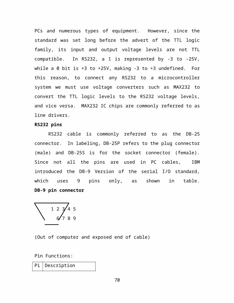
Selecting RF transmitters requires an understanding of modulation methods such
as AM and FM. On-off key (OOK), the simplest form of modulation, consists of turning
the signal on or off. Amplitude modulation (AM) causes the base band signal to vary the
amplitude or height of the carrier wave to create the desired information content.
Frequency modulation (FM) causes the instantaneous frequency of a sine wave carrier to
depart from the center frequency by an amount proportional to the instantaneous value of
the modulating signal. Amplitude shift key (ASK) transmits data by varying the
amplitude of the transmitted signal. Frequency shift key (FSK) is a digital modulation
scheme using two or more output frequencies. Phase shift key (PSK) is a digital
modulation scheme in which the phase of the transmitted signal is varied in accordance
with the base band data signal.
Additional considerations when selecting RF transmitters include supply voltage,
supply current, RF connectors, special features, and packaging. Some RF transmitters
include visual or audible alarms or LED indicators that signal operating modes such as
power on or reception. Other devices attach to coaxial cables or include a connector or
port to which an antenna can be attached. Typically, RF transmitters that are rated for
outdoor use feature a heavy-duty waterproof design. Devices with internal calibration and
a frequency range switch are also available.
RF transmitters are used in a variety of applications and industries. Often, devices
that are used with integrated circuits (ICs) incorporate surface mount technology (SMT),
through hole technology (THT), and flat pack. In the telecommunications industry, RF
transmitters are designed to fit in a metal rack that can be installed in a cabinet. RF
transmitters are also used in radios and in electronic article surveillance systems (EAS)
found in retail stores. Inventory management systems use RF transmitters as an
alternative to barcodes.
70

RF transmitter ST-TX01-ASK:
General Description:
The ST-TX01-ASK is an ASK Hybrid transmitter module. The ST-TX01-ASK is
designed by the Saw Resonator, with an effective low cost, small size, and simple-to-use
for designing.
Frequency Range: 315 / 433.92 MHZ.
Supply Voltage: 3~12V.
Output Power: 4~16dBm
Circuit Shape: Saw
Applications
Wireless security systems
Car Alarm systems
Remote controls.
Sensor reporting
Automation systems
71

Fig 13: Pin Description of the Transmitter module
72

Fig 14: Interfacing TX module to a Micro controller
RF ENCODER (HT12E):
Features
_ Operating voltage
_ 2.4V~5V for the HT12A
_ 2.4V~12V for the HT12E
_ Low power and high noise immunity CMOS technology
_ Low standby current: 0.1_A (typ.) at VDD=5V
_ HT12A with a 38kHz carrier for infrared transmission medium
_ Minimum transmission word
_ Four words for the HT12E
_ One word for the HT12A
_ Built-in oscillator needs only 5% resistor
_ Data code has positive polarity
_ Minimal external components
_ HT12A/E: 18-pin DIP/20-pin SOP package
Applications
_ Burglar alarm system
_ Smoke and fire alarm system
_ Garage door controllers
_ Car door controllers
73

_ Car alarm system
_ Security system
_ Cordless telephones
_ Other remote control systems
General Description
The 212 encoders are a series of CMOS LSIs for remote control system applications.
They are capable of encoding information which consists of N address bits and 12_N data
bits. Each address/data input can be set to one of the two logic states. The programmed
addresses/data are transmitted together with the header bits via an RF or an infrared
transmission medium upon receipt of a trigger signal. The capability to select a TE
trigger on the HT12E or a DATA trigger on the HT12A further enhances the application
flexibility of the 212 series of encoders. The HT12A additionally provides a 38kHz
carrier for infrared systems.
74

Note: Address/Data represents pins that can be address or data according to the decoder
requirement.
Fig 15: Block diagram of HT 12E Encoder
Pin Description:
Fig 16: Pin description of HT12E
75
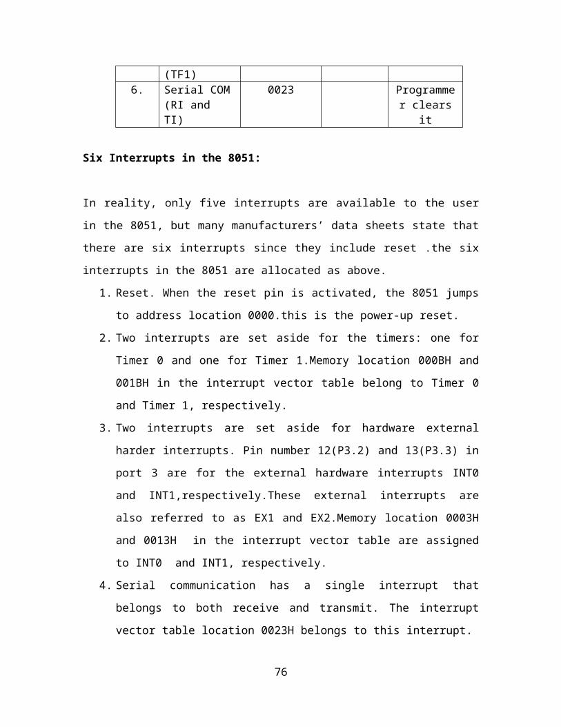
Note: D8~D11 are all data input and transmission enable pins of the HT12A.
TE is a transmission enable pin of the HT12E.
Absolute Maximum Ratings
Supply Voltage (HT12A) .............._0.3V to 5.5V
Storage Temperature................._50_C to 125_C
Operating Temperature..............._20_C to 75_C
Supply Voltage (HT12E) ..............._0.3V to 13V
Input Voltage....................VSS_0.3 to VDD+0.3V
76

77

Fig 17: Timing diagram of the HT12E and HT12A
78

Application Circuits:
Fig 18: Application circuit of HT12E
Flow Chart:
Fig 19: Flow chat for data transmission in HT12E
79

RF receiver section:
RF receivers are electronic devices that separate radio signals from one another
and convert specific signals into audio, video, or data formats. RF receivers use an
antenna to receive transmitted radio signals and a tuner to separate a specific signal from
all of the other signals that the antenna receives. Detectors or demodulators then extract
information that was encoded before transmission. There are several ways to decode or
modulate this information, including amplitude modulation (AM) and frequency
modulation (FM). Radio techniques limit localized interference and noise. With direct
sequence spread spectrum, signals are spread over a large band by multiplexing the signal
with a code or signature that modulates each bit. With frequency hopping spread
spectrum, signals move through a narrow set of channels in a sequential, cyclical, and
predetermined pattern.
Selecting RF receivers requires an understanding of modulation methods
such as AM and FM. On-off key (OOK), the simplest form of modulation, consists of
turning the signal on or off. Amplitude modulation (AM) causes the base band signal to
vary the amplitude or height of the carrier wave to create the desired information content.
Frequency modulation (FM) causes the instantaneous frequency of a sine wave carrier to
depart from the center frequency by an amount proportional to the instantaneous value of
the modulating signal. Amplitude shift key (ASK) transmits data by varying the
amplitude of the transmitted signal. Frequency shift key (FSK) is a digital modulation
scheme using two or more output frequencies. Phase shift key (PSK) is a digital
modulation scheme in which the phase of the transmitted signal is varied in accordance
with the base band data signal.
RF receivers vary in terms of performance specifications such as
sensitivity, digital sampling rate, measurement resolution, operating frequency, and
communication interface. Sensitivity is the minimum input signal required to produce a
specified output signal having a specified signal-to-noise (S/N) ratio. Digital sampling
rate is the rate at which samples can be drawn from a digital signal in kilo samples per
second. Measurement resolution is the minimum digital resolution, while operating
frequency is the range of received signals. Communication interface is the method used
80

to output data to computers. Parallel interfaces include general-purpose interface bus
(GPIB), which is also known as IEEE 488 and HPIB Protocol. Serial interfaces include
universal serial bus (USB), RS232, and RS485.
Additional considerations when selecting RF receivers include supply
voltage, supply current, receiver inputs, RF connectors, special features, and packaging.
Some RF receivers include visual or audible alarms or LED indicators that signal
operating modes such as power on or reception. Other devices attach to coaxial cables or
include a connector or port to which an antenna can be attached. Typically, RF receivers
that are rated for outdoor use feature a heavy-duty waterproof design. Devices with
internal calibration and a frequency range switch are also available.
RF receiver ST-RX04-ASK:
Description:
The RX04 is a low power ASK receiver IC which is fully compatible with
the MitelKESRX01 IC and is suitable for use in a variety of low power radio applications
including remote keyless entry. The RX04 is based on a single-
Conversion, super-heterodyne receiver architecture and incorporates an entire phase-
locked loop (PLL) for precise local oscillator generation.
Applications:
Car security system
Wireless security systems
Sensor reporting
automation system
Remote Keyless entry
Features
Low power consumption.
Easy for application.
On-Chip VCO with integrated PLL using crystal oscillator reference.
81

Integrated IF and data filters.
Operation temperature range : 10﹣ ℃~+60℃
Operation voltage: 5 Volts.
Available frequency at : 315/434 MHz
Functional description:
Fig 20: RF receiver module.
RF DECODER (HT 12D):
Features
_ Operating voltage: 2.4V~12V
_ Low power and high noise immunity CMOS technology
_ Low standby current
_ Capable of decoding 12 bits of information
_ Binary address setting
_ Received codes are checked 3 times
_ Address/Data number combination
_ HT12D: 8 address bits and 4 data bits
_ HT12F: 12 address bits only
82

_ Built-in oscillator needs only 5% resistor
_ Valid transmission indicator
_ Easy interface with an RF or an infrared transmission medium
_ Minimal external components
_ Pair with Holteks 212 series of encoders
_ 18-pin DIP, 20-pin SOP package
Applications
_ Burglar alarm system
_ Smoke and fire alarm system
_ Garage door controllers
_ Car door controllers
_ Car alarm system
_ Security system
_ Cordless telephones
_ Other remote control systems
General Description
The 212 decoders are a series of CMOS LSIs for remote control system
applications. They are paired with Holteks 212 series of encoders (refer to the
encoder/decoder cross reference table). For proper operation, a pair of encoder/decoder
with the same number of addresses and data format should be chosen. The decoders
receive serial addresses and data from a programmed 212 series of encoders that are
transmitted by a carrier using an RF or an IR transmission medium. They compare the
serial input data three times continuously with their local addresses. If no error or
unmatched codes are found, the input data codes are decoded and then transferred to the
output pins. The VT pin also goes high to indicate a valid transmission. The 212 series of
decoders are capable of decoding informations that consist of N bits of address and 12_N
bits of data. Of this series, the HT12D is arranged to provide 8 address bits and 4 data
bits, and HT12F is used to decode 12 bits of address information.
83
Notes: Data type: L stands for latch type data output.
VT can be used as a momentary data output.
Fig 21: Block Diagram of HT 12D Decoder
Note: The address/data pins are available in various combinations (see the address/data
table).
84
Pin Assignment:
Fig 22: Pin diagram of HT12D
Absolute Maximum Ratings
Supply Voltage .........................................._0.3V to 13V
Storage Temperature ............................_50_C to 125_C
Input Voltage ................................VSS_0.3 to VDD+0.3V
Operating Temperature..........................._20_C to 75_C
85

Functional Description
Operation
The 212 series of decoders provides various combinations of addresses and data pins in
different packages so as to pair with the 212 series of encoders. The decoders receive data
that are transmitted by an encoder and interpret the first N bits of code period as
addresses and the last 12_N bits as data, where N is the address code number. A signal on
the DIN pin activates the oscillator, which in turn decodes the incoming address and data.
The decoders will then check the received address three times continuously. If the
received address codes all match the contents of the decoders local address, the 12_N bits
of data are decoded to activate the output pins and the VT pin is set high to indicate a
valid transmission. This will last unless the address code is incorrect or no signal is
received. The output of the VT pin is high only when the transmission is valid. Otherwise
it is always low.
Output type
Of the 212 series of decoders, the HT12F has no data output pin but its VT pin can be
used as a momentary data output. The HT12D, on the other hand, provides 4 latch type
data pins whose data remain unchanged until new data are received.
86

Fig 23: Timing Diagram of Decoder HT12D
Fig 24: Application circuit of HT12D
87

Flowchart
The oscillator is disabled in the standby state and activated when a logic _high_ signal
applies to the DIN pin. That is to say, the DIN should be kept low if there is no signal
input.
Fig 25: Flow chart of HT12D for data transmission
88
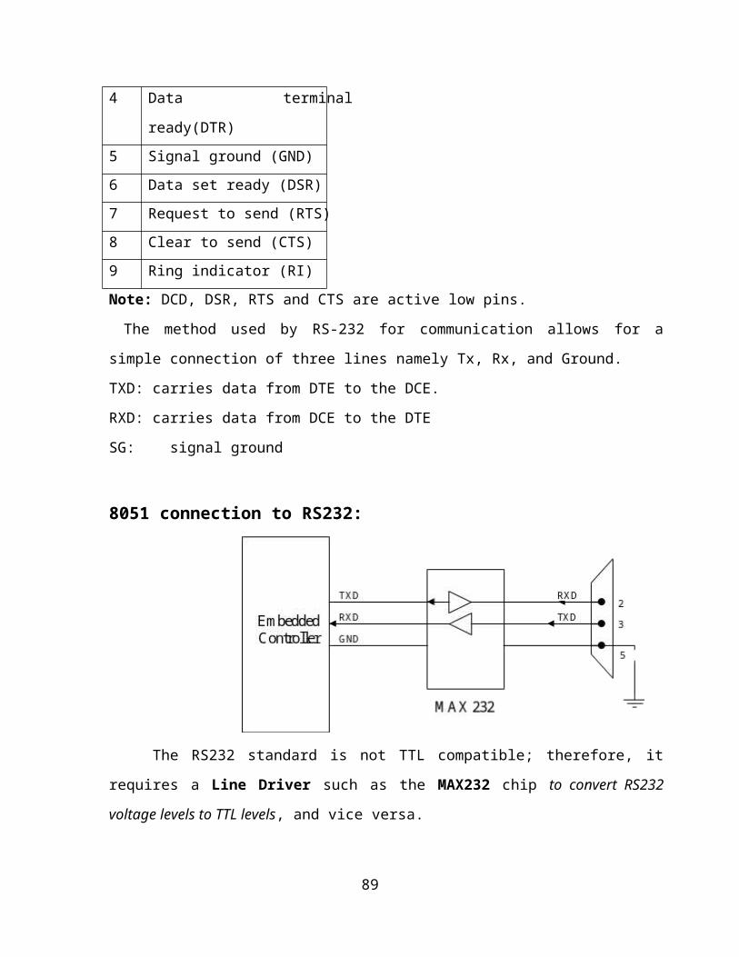
7. SOFTWARE COMPONENTS
ABOUT SOFTWARE
Software used is:
*Keil software for C programming
*Express PCB for lay out design
*Express SCH for schematic design
*Embedded C
7.1 KEIL µVision3
What's New in µVision3?
µVision3 adds many new features to the Editor like Text Templates, Quick Function
Navigation, and Syntax Coloring with brace high lighting Configuration Wizard for dialog
based startup and debugger setup. µVision3 is fully compatible to µVision2 and can be used in
parallel with µVision2.
What is µVision3?
µVision3 is an IDE (Integrated Development Environment) that helps you write, compile, and
debug embedded programs. It encapsulates the following components:
A project manager.
A make facility.
Tool configuration.
Editor.
A powerful debugger.
89

7.2 Express PCB
Express PCB is a Circuit Design Software and PCB manufacturing service. One can
learn almost everything you need to know about Express PCB from the help topics included
with the programs given.
Details:
Express PCB, Version 5.6.0
7.3 Express SCH
The Express SCH schematic design program is very easy to use. This software enables
the user to draw the Schematics with drag and drop options.
A Quick Start Guide is provided by which the user can learn how to use it.
Details:
Express SCH, Version 5.6.0
7.4 EMBEDDED C:
The programming Language used here in this project is an Embedded C
Language. This Embedded C Language is different from the generic C language in few things
like
a) Data types
b) Access over the architecture addresses.
The Embedded C Programming Language forms the user friendly language with access over
Port addresses, SFR Register addresses etc.
90
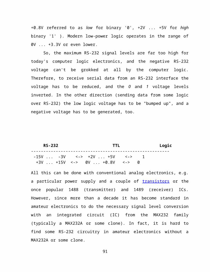
Embedded C Data types:
Data Types Size in Bits Data Range/Usage
unsigned char 8-bit 0-255
signed char 8-bit -128 to +127
unsigned int 16-bit 0 to 65535
signed int 16-bit -32,768 to +32,767
sbit 1-bit SFR bit addressable only
Bit 1-bit RAM bit addressable only
sfr 8-bit RAM addresses 80-FFH only
Unsigned char:The unsigned char is an 8-bit data type that takes a value in the range of 0-255(00-
FFH). It is used in many situations, such as setting a counter value, where there is no need for
signed data we should use the unsigned char instead of the signed char. Remember that C
compilers use the signed char as the default if we do not put the key word
Signed char:The signed char is an 8-bit data type that uses the most significant bit (D7 of D7-D0)
to represent the – or + values. As a result, we have only 7 bits for the magnitude of the signed
number, giving us values from -128 to +127. In situations where + and – are needed to
represent a given quantity such as temperature, the use of the signed char data type is a must.
Unsigned int:The unsigned int is a 16-bit data type that takes a value in the range of 0 to 65535
(0000-FFFFH).It is also used to set counter values of more than 256. We must use the int data
type unless we have to. Since registers and memory are in 8-bit chunks, the misuse of int
91

variables will result in a larger hex file. To overcome this we can use the unsigned char in
place of unsigned int.
Signed int: Signed int is a 16-bit data type that uses the most significant bit (D15 of D15-D0) to
represent the – or + value. As a result we have only 15 bits for the magnitude of the number or
values from -32,768 to +32,767.
Sbit (single bit): The sbit data type is widely used and designed specifically to access single bit
addressable registers. It allows access to the single bits of the SFR registers.
Accessing SFR addresses 80-FFH
Another way to access the SFR RAM space 80-FFH is to use the sfr data type. This is
shown in the below example .Both the bit and byte addresses for the P0-P3 ports are given in
the table. Notice in the given example that there is no #include<reg51.h> statement which
allows us to access any byte of the SFR RAM space 80-FFH.
Single Bit Addresses of Ports
P0 Addr P1 Addr P2 Addr P3 Addr Ports Bit
P0.0 80H P1.0 90H P2.0 A0H P3.0 B0H D0
P0.1 81H P1.1 91H P2.1 A1H P3.1 B1H D1
P0.2 82H P1.2 92H P2.2 A2H P3.2 B2H D2
P0.3 83H P1.3 93H P2.3 A3H P3.3 B3H D3
P0.4 84H P1.4 94H P2.4 A4H P3.4 B4H D4
P0.5 85H P1.5 95H P2.5 A5H P3.5 B5H D5
P0.6 86H P1.6 96H P2.6 A6H P3.6 B6H D6
P0.7 87H P1.7 97H P2.7 A7H P3.7 B7H D7
92

DATA CONVERTION PROGRAMS IN EMBEDDED CMany micro-controllers have a real time clock (RTC) where the time and date are
kept even when the power is off. These time and date are often in packed BCD by RTC. To
display them they must be converted to ASCII. So, in this topic we are showing application of
logic and instructions in the conversion of BCD and ASCII.
ASCII numbers
On ASCII key boards, when the key “0” is activated, “0110000” (30h) is
provided to the system. Similarly 31h (0110001) is provided for the key “1”, and so on as
shown in the table
Packed BCD to ASCII conversion
The RTC provides the time of day (hour, minutes, seconds) and the date (year,
month, day) continuously, regardless of whether the power is ON or OFF. In the conversion
procedure the packed BCD is first converted to unpacked BCD. Then it is tagged with 0110000
(30h).
ASCII code for Digits 0-9
Key ASCII (hex) Binary BCD (unpacked)
0 30 011 0000 0000 0000
1 31 011 0001 0000 0001
2 32 011 0010 0000 0010
3 33 011 0011 0000 0011
4 34 011 0100 0000 0100
5 35 011 0101 0000 0101
6 36 011 0110 0000 0110
7 37 011 0111 0000 0111
8 38 011 1000 0000 1000
9 39 011 1001 0000 1001
93
ASCII to packed BCD conversion
To convert ASCII to packed BCD it is first converted to unpacked and then combined
to make packed BCD. For example 4 and 7 on the keyboard give 34h and 37h respectively the
goal is to produce 47h or “0100 0111” which is packed BCD.
Key ASCII unpacked BCD packed BCD
4 34 00000100
7 37 00000111
01000111 or 47h
Checksum byte in ROM
To ensure the integrity of ROM contents, every system must perform the checksum
calculation. The process of checksum will detect any corruption of the contents of ROM. One
of the cause of the ROM corruption is current surge either when the system is turned on or
during operation. To ensure data integrity in ROM the checksum process uses, what is a
checksum byte. The is an extra byte that is tagged to the end of the series of the of data.
To calculate the checksum byte of a series of bytes of data, the following steps can be used
1) Add the bytes together and drop the carries.
2) Take the 2’s complement of the total sum. This is the checksum byte , which becomes
the last byte of the series
Binary (hex) to decimal and ASCII conversion in embedded CIn C-language we use a function call “printf” which is standard IO library function
doing the conversions of data from binary to decimal, or vice versa. But here we are using our
own functions for conversions because it occupies much of memory.
One of the most commonly used is binary to decimal conversion. In devices such as
ADC chips the data is provided to the controller in binary. In order to display binary data we
need to convert it to decimal and then to ASCII. Since the hexadecimal format is a convenient
way of representing binary data we refer to binary data as hex. The binary data 00-FFH
converted to decimal will give us 000 to 255.
94
One way to do this is to divide it by 10 and keep the remainder, for example
11111101 or FDH is 253 in decimal. The following is one version of the algorithm for
conversion of hex (binary) to decimal.
Quotient Remainder
FD/0A 19 3(low digit) LSD
19/0A 2 5(middle digit)
95

SOURCE CODE#include<reg51.h>
void serinit()
{
TMOD = 0x20;
TH1 = 0xFD;
TL1 = 0xFD;
SCON = 0x50;
TR1= 1;
}
void srstring(unsigned char value)
{
SBUF=value;
while(TI==0);TI=0;
}
void delay(unsigned int value)
{
unsigned int i,j;
for(i=0;i<=value;i++)
96

for(j=0;j<=1275;j++);
}
void main()
{
unsigned char i;
serinit();
srstring("welcome");
srtx(0x0a);srtx(0x0d);
while(1)
{
i=P2;
delay(1);
srtx(0x0d);
if(i=!0xff)
{
Srsting(“fire accident”);
srtx(0x0d);
srtx(0x0a);
}
}
97
CONCLUSION
The project “role of wirless sensor network in forest fire prevention ” has been
successfully designed and tested. Integrating features of all the hardware components used
have developed it. Presence of every module has been reasoned out and placed carefully thus
contributing to the best working of the unit. Secondly, using highly advanced IC’s and with the
help of growing technology the project has been successfully implemented.
98

FUTURE ASPECTS
The parameters used in this project can be extended. This whole project can be made as
one node and these nodes can be placed at various places in the forest. The communication
between these nodes and coordinators can be made easy by using zigbee modules. This project
can be extended by using the zigbee network which can be easy to monitor the various
locations in big industries or security for many more places
99

BIBLIOGRAPHY
NAME OF THE SITES:
1. WWW.MITEL.DATABOOK.COM
2. WWW.ATMEL.DATABOOK.COM
3. WWW.FRANKLIN.COM
4. WWW.microC.COM
REFERENCES
1. Design with pic microcontrollers by jhon B.peatman
2. Fundamentals of Embedded software by Daniel W Lewis
3. The 8051 microcontroller and embedded systems by Mohammad Ali
Mazaidi
4. Antennas and wave propagation by K.D.Prasad
100