robust decentralized voltage control of dc-dc converters with applications to power...
TRANSCRIPT

Robust Decentralized Voltage Control of DC-DC Converters withApplications to Power Sharing and Ripple Sharing
Mayank Baranwal1,a, Srinivasa M. Salapaka1,b and Murti V. Salapaka2,c
Abstract— This paper addresses the problem of output volt-age regulation for multiple DC-DC converters connected to agrid, and prescribes a robust scheme for sharing power amongdifferent sources. Also it develops a method for sharing 120 Hzripple among DC power sources in a prescribed proportion,which accommodates the different capabilities of DC powersources to sustain the ripple. We present a decentralized controlarchitecture, where a nested (inner-outer) control design is usedat every converter. An interesting aspect of the proposed designis that the analysis and design of the entire multi-convertersystem can be done using an equivalent single converter system,where the multi-converter system inherits the performance androbustness achieved by a design for the single-converter system.Another key aspect of this work is that the voltage regulationproblem is addressed as a disturbance-rejection problem, whereunknown load current is viewed as an external signal, andthus, no prior information is required on the nominal loadingconditions. The control design is obtained using robust optimal-control framework. Case studies presented show the enhancedperformance of prescribed optimal controllers.
I. INTRODUCTION
In power network topologies, especially in microgrids [1],multiple DC power sources connected in parallel (see Figure1), each interfaced with DC-DC converter, provide power attheir common output, the DC-link, at a regulated voltage;this power can directly feed DC loads or be used by aninverter to interface with AC loads . Voltage controllersform an integral component of DC-DC converters in suchsystems. A paralleled architecture for multiple power sourcesis preferred since it enables higher output power, higherreliability and ease of use [2]. Here two main controlarchitectures are adopted - (1) master-slave control, wherethe voltage regulation error from the master converter isutilized to provide an error signal to all the parallel con-nected converters [2], [3], (2) decentralized control, whereeach converter utilizes an independent and variable voltagereference depending on the output of each unit [4], [5].Irrespective of the control framework, controllers at eachconverter are to be designed such that the voltage at the DC-link is regulated at a prescribed setpoint. Another importantcontrol objective is to ensure that the DC sources providepower in a prescribed proportion, which may be dictatedby their power ratings or external economic criteria. Themain challenges arise from the uncertainties in the size andthe schedules of loads, the complexity of a coupled multi-converter network, the uncertainties in the model parameters
1Department of Mechanical Science and Engineering, University ofIllinois at Urbana-Champaign, IL 61801, USA
2Department of Electrical and Computer Engineering, University ofMinnesota, Minneapolis, MN 55455 USA
[email protected], [email protected]@umn.edu
Fig. 1: A schematic of a microgrid. An array of DC sources providepower for AC loads. Power sources provide power at DC-link,their common output bus, at a voltage that is regulated to a set-point. The control system at the respective DC-DC converter thatinterfaces with a source is responsible for regulating the voltage athe DC-link. An inverter that connects to the DC-link converts thetotal current from the sources at the regulated voltage to alternatingcurrent (AC) at its output to satisfy the power demands of the ACloads. This paper describes an approach for control design of themultiple converters systems associated with power transfer fromsources to the DC-link (shown by the dotted line).
at each converter, and the adverse effects of interfacing DCpower sources with AC loads, such as the 120 Hz ripple thathas to be provided by the DC sources.
Problems related to robust and optimal design of convertercontrollers have received recent attention. In [6], a linear-matrix-inequality (LMI) based robust control design forboost converters has resulted in significant improvementsover conventional PID-based controllers. Use of H∞ frame-work in context of inverter systems has also been studiedin [7]–[9]. While the issue of current sharing is extensivelystudied [4], [10]–[12], most methods assume a single powersource. A systematic control design that addresses all thechallenges and objectives for the multi-converter control isstill lacking.
In this paper, we develop a control architecture that ad-dresses the following primary objectives for multi-convertercontrol - (1) voltage regulation at the DC-link while guar-anteeing robustness of the closed-loop system performanceto load and parametric uncertainties, (2) prescribed powersharing among a number of parallel converters, (3) control-ling the tradeoff between 120 Hz ripple on the total currentprovided by the power sources and the ripple on the DC-linkvoltage, and (4) 120 Hz DC output ripple sharing amongconverters. The tradeoffs with 120 Hz ripple in objectives
2016 American Control Conference (ACC)Boston Marriott Copley PlaceJuly 6-8, 2016. Boston, MA, USA
978-1-4673-8682-1/$31.00 ©2016 AACC 7444

(3) and (4) result from a direct consequence of interfacingDC-power sources with AC loads (see Figure 1). If weassume negligible power losses at the inverter and the loadbus, the power provided by power sources at the DC-linkshould equal to the power consumed by the AC loads, that is,
V i = (V sin ωt)(I sin(ωt+φ)) =V I
2(cosφ+cos(2ωt+φ).
Since the instantaneous power has a 2ω = 120 Hz ripple, thecurrent i =
∑ik at the DC-link has to provide for this 120
Hz component. The total ripple demand posed by the AC-grid side is met partly by the ripple current sourced by a ca-pacitor iC which reduces the magnitude of the ripple currentto be provided by the DC source via the converters. However,greater the ripple magnitude in the capacitor current greaterwill be the ripple in the capacitor voltage, thus adverselyaffecting voltage regulation. Therefore a compromise has tobe reached in the allowable ripple in the capacitor current andthe ripple provided by the DC sources. The control schemepresented in the article provides a “knob” to adjust therelative ratio of how the 120 Hz ripple is shared between thetwo quantities - the sourced current i and the output voltageV . Moreover in a scenario where multiple and differenttypes of DC sources are employed, it is often the case thatthe tolerance to ripple varies. Here it becomes importantto allocate greater percentage of ripple load to tolerant DCsources while reducing the ripple load on vulnerable DCsources. The article presents a controller synthesis procedurewhere the 120 Hz ripple on the current i can be shared amongthe paralleled DC sources (ik) in a pre-specified proportion.
An important aspect of the proposed control architecture isthat it is decentralized and addresses all the objectives simul-taneously. Moreover we show that for the control approachdescribed in the paper, the control design and the closed-loopanalysis of the multi-converter system can be completelycharacterized in terms of an appropriate single-convertersystem; thereby significantly reducing the complexity inaddressing multi-converter systems. This architecture ex-ploits structural features of the paralleled multi-convertersystem, which results in a modular and yet coordinatedcontrol design. For instance, it exploits that the voltageregulation objective is common to all the converters, andthat the differences in demands on different converters aremainly in terms of their output currents; accordingly at eachconverter, it employs a nested (outer-voltage inner-current)control structure [13], where the outer loop is responsible forrobust voltage regulation and the inner loop for shaping thecurrents. The structure of control for each inner-loop is sochosen that the entire closed-loop multi converter system canbe reduced to an equivalent single-converter system in termsof the transfer function from the desired regulation setpointVdes to the voltage V . Furthermore, for the outer-controldesign, the load current is treated as an external disturbanceand the voltage regulation problem is cast as a disturbancerejection problem in an optimal control setting. This design,besides achieving the voltage-regulation objective, providesrobustness to deviations from the structural assumptions inthe control design. Note that this viewpoint is in contrast totypical methods in existing literature, where voltage regula-tion in presence of unknown loads is addressed either using
adaptive control [14], or by letting the voltage droop in acontrolled manner.
II. MODELING OF CONVERTERS
In this section, we provide dynamic models for DC-DCconverters, which convert a source of direct current (DC)from one voltage level to another. The models presentedbelow depict dynamics for signals that are averaged overa switch cycle.
A schematic of the Boost converter is shown in Fig. 2(a).A dynamic model (averaged over switching cycles) is givenby,
L ˙iL(t) = −(1−d(t))V (t)+Vg, CV (t) = (1−d(t))iL(t)−iload,
where d(t) represents the duty-cycle (or the proportion ofON duration) at time t, which by defining d′(t) = 1 − d(t)and D′ =
Vg
Vdescan be rewritten as
L ˙iL(t) = −d′(t)V (t) + Vg︸ ︷︷ ︸u(t):=Vg−u(t)
, CV (t) = (D′ + d′)︸ ︷︷ ︸≈D′
iL(t)− iload.
Here Vdes represents the desired output voltage and d =d′(t)−D′ is typically very small, which allows for a linearapproximation around the nominal duty-cycle, D = 1 −D′given by,
LdiL(t)
dt= u(t), C
dV (t)
dt≈ D′iL(t)− iload.
Fig. 2(b) depicts the circuit schematic of a buck converterwith an ideal switch. The averaged model of a buck converteris given by,
LdiL(t)
dt= −V (t) + d(t)Vg︸ ︷︷ ︸
u(t):=−V (t)+u(t)
, CdV (t)
dt= iL(t)− iload.
The electronic circuit of a buck-boost converter is shownin Fig. 2(c). As in case of a boost converter, we definenominal duty-cycle, D = Vdes
Vdes−Vg= 1 − D′. A linear
approximation of the above dynamical equations yields,
L ˙iL(t) = V (t) + d(t)(Vg − V (t))︸ ︷︷ ︸u(t):=V (t)+u(t)
, CV (t) ≈ −D′iL(t)− iload
III. CONTROL FRAMEWORK FOR A SINGLE-CONVERTER
In this section, we describe the inner-current outer-voltagecontrol architecture for a single DC-DC converter. The keyobjectives of the control design are - (1) voltage regulation inpresence of uncertain loads, and (2) 120 Hz ripple sharingcontrol between iL and iC . We first consider the case ofa boost converter control design, the dynamics of which isgiven by
iL(s) =1
sL(Vg(s)− u(s)), V (s) =
1
sC(D′iL(s)− iload(s)),
(1)and the corresponding block-diagram representation of
above set of equations is shown in Fig. 3, the controlobjectives are to design u (equivalently u) such that voltageregulation error Vdes − V is made small irrespective of loaddisturbances iload and variations in parameters L and C,and achieve a prescribed tradeoff between |iL(j2π120)| and|iC(j2π120)|.
These two objectives are achieved using a nested inner-current outer-voltage control architecture, shown in Fig. 4
7445

(a) (b) (c)Fig. 2: Circuit representing (a) Boost converter, (b)Buck converter, and (c) Buck-Boost converter. Note that iload includes both the nominalload current, as well as ripple current. The converters are assumed to operate in continuous-conduction-mode (CCM). Boost convertersstep up the voltage at the output, while buck converters step down the voltage. A buck-boost converter can achieve both the objectives.
Fig. 3: Block diagram representation of a boost-type converter.The control signal u is converted to an equivalent PWM signal tocommand the gate of the transistor acting as a switch.
(here Gc = 1sL and Gv = 1
sC ). The voltage controllerKv generates a current reference for the current controllerKc. The current controller Kc is designed to achieve ahigh closed inner-loop bandwidth with ripple control as anobjective, whereas the voltage controller Kv is designedto achieve a relatively lower closed outer-loop bandwidthwith DC (zero frequency) voltage regulation as its primaryobjective. We assume that the quantities - output voltage Vand inductor current iL are available for measurement.
Design of the outer-loop controller: For a given controllerKc for the inner-loop, the closed outer-loop signals ofinterest are given by (see Figure 4)
Vdes − V = SVdes +GvSd+ Tn (2)
iL = GcKvSVdes +1
D′Td−KvGcSn (3)
iref = Kv(SVdes +GvSd)−KvSn, (4)
where d denotes the load current iload (shown as disturbanceto the plant), n denotes the voltage measurement noise, Gcrepresents the closed inner-loop transfer function from iref toiL, and T (s) and S(s) are closed-loop complementary sensi-tivity and sensitivity transfer functions respectively, describedby,
T (s) = (I +GvD′GcKv)
−1(GvD′GcKv),
S(s) = (I +GvD′GcKv)
−1. (5)
The voltage-regulation objective, as evident from Eq. 2,
Fig. 4: Block diagram representation of the inner-outer controldesign. Exogenous signals Vdes and iload represent the desiredoutput voltage and disturbance, respectively. The quantities V andiL represent the available measurements.
requires designing Kv such that |S(jω)| is small at the
frequencies where disturbance d is prominent. However thisimplies that the effect of d on the inductor current iL (see Eq.3) is larger since |T (jω)| is larger in those frequencies (fromEq. 5). Therefore there is a fundamental trade-off betweenvoltage regulation and minimizing effects of disturbances (orload current iload) in iL. Also to diminish the effect of noiseon voltage regulation, the control design should be such thatthe closed-loop map T rolls of at frequencies beyond thedisturbance bandwidth. Furthermore low iref is ensured ifKvS can be made small. The controller Kv is obtained bycasting these multiple objectives in the following optimalcontrol problem [15],
minKv∈K
∥∥∥∥∥ WsSWuKvSWtT
∥∥∥∥∥∞
, (6)
where the weights Ws, Wt and Wu are chosen to reflectthe design specifications of robustness to disturbances andparametric uncertainties, tracking bandwidth, and saturationlimits on the control signal. For example, the weight functionWs(jω) is chosen to be large in frequency range [0, ωBW ]to ensure a small tracking error e = Vdes − V in thisfrequency range. The weight function Wt(jω) is designedas a high-pass filter to ensure that T (jω) is small at highfrequencies to provide mitigation to measurement noise. Thedesign of constant Wu entails ensuring that the control effortlies within saturation limits. The resulting controller is robustto disturbances up to ωBW , which accounts for variations inload disturbances as well as parametric uncertainties.
Design of the inner-loop controller: The outer-loop con-trol design assumed the inner closed-loop Gc. Here wepropose an inner-loop control design that results in a second-order transfer function Gc, thereby ensuring a relatively low-order optimal controller Kv . The main objective for design-ing the inner-loop controller Kc is to decide the trade-offbetween the 120 Hz ripple on the voltage V (equivalently onthe capacitor current ic) and the output current i (equivalentlyiL) of the converter. Accordingly, we design Kc such that
Gc(s) =
(ω
s+ ω
)(s2 + 2ζ1ω0s+ ω2
0
s2 + 2ζ2ω0s+ ω20
), (7)
where ω0 = 2π120 rad/s. ω, ζ1, ζ2 are design parameters.Here the parameter ω > ω0 is simply chosen to implement alow-pass filter that attenuates undesirable frequency contentin iL beyond ω. Note that in this design of Gc, there is anotch at ω0 = 120 Hz, the size of this notch is determinedby the ratio ζ1
ζ2(see Figure 5). Lower values of this ratio
correspond to larger notches, which in turn imply smaller 120Hz component in iL, since Gc represents the inner closed-loop transfer function from iref to iL. Furthermore since iC =iload − iL, this in turn implies higher ripples in iC . Thus theratio ζ1
ζ2can be appropriately designed to achieve a specified
7446
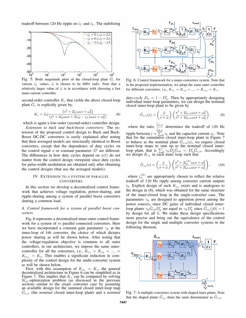
tradeoff between 120 Hz ripple on iC and iL. The stabilizing
Fig. 5: Bode magnitude plots of the closed-loop plant Gc forvarious ζ1 values. ω is chosen to be 600π rad/s. Note that arelatively larger value of ω is in accordance with choosing a fastinner-current controller.
second-order controller Kc that yields the above closed-loopplant Gc is explicitly given by,
Kc = Lω
(s2 + 2ζ1ω0s+ ω2
0
)(s2 + 2ζ2ω0s+ 2(ζ2 − ζ1)ω0ω + ω2
0), (8)
which is again a low-order (second-order) controller design.Extension to buck and buck-boost converters: The ex-
tension of the proposed control design to Buck and Buck-Boost DC-DC converters is easily explained after notingthat their averaged models are structurally identical to Boostconverters, except that the dependence of duty cycles onthe control signal u or constant parameter D′ are different.The differences in how duty cycles depend on u(t) do notmatter from the control design viewpoint since duty cyclesfor pulse-width modulation are obtained only after obtainingthe control designs (that use the averaged models).
IV. EXTENSION TO A SYSTEM OF PARALLELCONVERTERS
In this section we develop a decentralized control frame-work that achieves voltage regulation, power-sharing, andripple-sharing among a system of parallel boost converterssharing a common load.
A. Control framework for a system of parallel boost con-verters
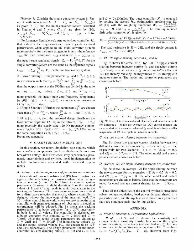
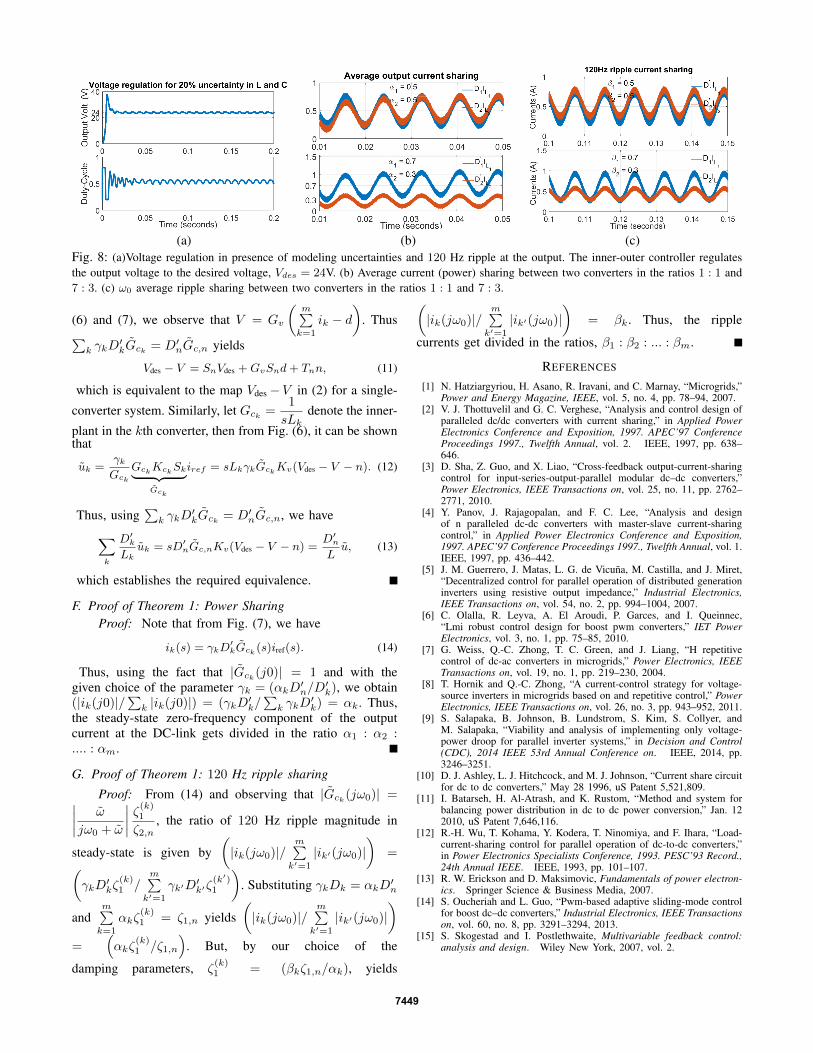
Fig. 6 represents a decentralized inner-outer control frame-work for a system of m parallel connected converters. Herewe have incorporated a constant gain parameter γk at theinner-loop of kth converter, the choice of which dictatespower sharing as will be shown below. After noting thatthe voltage-regulation objective is common to all outercontrollers, in our architecture, we impose the same outer-controller for all the converters, i.e., Kv1 = Kv2 = .... =Kvm = Kv . This enables a significant reduction in com-plexity of the control design for the multi-converter systemas will be shown below.
First, with this assumption of Kvk = Kv , the generaldecentralized architecture in Figure 6 can be simplified as inFigure 7. This implies that Kv can be computed by solvingH∞-optimization problem (as discussed in the previoussection) similar to the single converter case by assumingan available design for the summed closed inner-loop mapGc,n (the nominal closed inner-loop plant) and a nominal
Fig. 6: Control framework for a many-converters system. Note thatin the proposed implementation, we adopt the same outer controllerfor different converters, i.e., Kv1 = Kv2 = .... = Kvm = Kv .
duty-cycle Dn = 1 − D′n. Then by appropriately designingindividual inner-loop parameters, we can design the nominalclosed inner-loop plant to be given by
Gc,n(s) =
(ω
s+ ω
)(s2 + 2ζ1,nω0s+ ω2
0
s2 + 2ζ2,nω0s+ ω20
), (9)
where the ratioζ1,nζ2,n
determines the tradeoff of 120 Hz
ripple between i =∑k ik and the capacitor current iC . Note
that for the cumulative closed inner-loop plant in Figure 7to behave as the nominal plant Gc,n(s), we require closedinner-loop maps to sum up to the nominal closed inner-loop plant, that is
∑k γkD
′kGck = D′nGc,n. Accordingly
we design Kck in each inner loop such that
Gck (s) =
(ω
s+ ω
)(s2 + 2ζ
(k)1 ω0s+ ω2
0
s2 + 2ζ2,nω0s+ ω20
), (10)
where ζ(k)1 are appropriately chosen to reflect the relativetradeoff of 120 Hz ripple among converter current outputsik. Explicit design of such Kck exists and is analogous tothe design in (8), which was obtained for the same structureof the inner-closed loop in the single-converter case. Theparameters γk are designed to apportion power among thepower sources, since DC gains of individual closed inner-loop plants γkGckD′k are equal to γkD′k since Gck(j0) = 1by design for all k. We make these design specificationsmore precise and bring out the equivalence of the controldesign for the single and multiple converter systems in thefollowing theorem.
Fig. 7: A multiple-converters system with shaped inner plants. Notethat the shaped plants Gck share the same denominator as Gc,n.
7447
Theorem 1: Consider the single-converter system in Fig-ure 4 with inductance L, D′ = D′n and Gc = Gc,n(s)as given in (9); and the multi-converter system describedin Figures 6 and 7 where Gck(s) are given by (10),∑k γkD
′kGck = D′nGc,n, and
∑k γk = 1, γk > 0 for
1 ≤ k ≤ m.1. [Performance Equivalence]: Any outer-loop controller Kv
that stabilizes the single-converter system yields identicalperformance when applied to the multi-converter system;more precisely, for the same exogenous inputs - the referenceVdes, the load disturbance iload, and noise n =
∑k γknk,
the steady-state regulated signals (Vdes−V,D′nLu, V ) for the
single-converter system are the same as the regulated signals
(Vdes − V,∑k
D′kLk
uk, V ) for the multi-converter system.
2. [Power Sharing]: If the parameters γk, and ζ(k)1 , 1 ≤ k ≤m are chosen such that γk =
αkD′n
D′k
andm∑k=1
αkζ(k)1 = ζ1,n,
then the output current at the DC-link get divided in the ratio
α1 : α2 : .... : αm, where 0 ≤ αk ≤ 1, andm∑k=1
αk = 1;
more precisely the steady-state zero-frequency components|i1(j0)| : |i2(j0)| : · · · : |im(j0)| are in the same proportionas α1 : α2 : .... : αm.3. [Ripple Sharing]: If further the parameters ζ(k)1 are chosen
such that ζ(k)1 =βkζ1,nαk
, wherem∑k=1
βk = 1, and 0 ≤ βk ≤
1,∀k ∈ 1, ..,m, then, the proposed design distributes theload current ripple (at 120Hz) in the ratio β1 : β2 : ... : βm;more precisely the steady-state 120 Hz-frequency compo-nents |i1(j2π120)| : |i2(j2π120)| : · · · : |im(j2π120)| are inthe same proportion as β1 : β2 : ... : βm.Proof: see appendix
V. CASE STUDIES: SIMULATIONS
In this section, we report simulation case studies, whichuse non-ideal components (such as diodes with non-zerobreakdown voltage, IGBT switches, stray capacitances, para-metric uncertainties) and switched level implementation toinclude nonlinearities associated with real-world experi-ments.
A. Voltage regulation in presence of parametric uncertaintiesConventional proportional-integral (PI) based control de-
signs exhibit satisfactory performance when the actual sys-tem parameters (L and C) lie ‘close’ to nominal systemparameters. However, a slight deviation from the nominalvalues of L and C may result in rapid degradation in thetracking performance. This issue becomes even more criticalfor a disturbance rejection framework, where a controller isdesigned without the knowledge of the uncertain load. TheH∞ robust control framework, where we seek an optimizingcontroller with guaranteed margins of robustness to modelinguncertainties will be adopted. Fig. 8a shows the trackingperformance of a boost converter for a 20% uncertaintyin both L and C values. The controller is designed fora boost converter with nominal L = 2.4mH and C =400µF, while the actual system parameters are chosen asL = 2mH and C = 500µF. The input source voltage Vgand the output desired voltage Vdes are chosen to be 12Vand 24V, respectively. The design parameters for the inner-controller Kc are: damping ratios ζ1 = 3.2 and ζ2 = 4.5,
and ω = 2π300rad/s. The outer-controller Kv is obtainedby solving the stacked H∞ optimization problem (see Eq.6) [15] with the weighting functions: Ws = 0.5s+2π50
s+0.06π50 ,Wu = 0.9, and Wt = s+2π40
0.05s+2π80 . The resulting reducedfifth-order controller Kv is given by:
Kv =0.256(s+ 113.9)(s+ 0.001)2(s2 + 4.05e4s+ 5.65e8)
(s+ 9.56)(s2 + 0.002s+ 4.8e− 6)(s2 + 9606s+ 8.8e7)
The load resistance is R = 24Ω, and the ripple current isIripple = 0.2 sin(2π120t)A.
B. 120 Hz ripple sharing between iL and iCFig. 9 shows the effect of ζ1 for 120 Hz ripple current
sharing between inductor current iL and capacitor currentiC . Clearly, smaller values of ζ1 impart notch-like effects at120 Hz, thereby reducing the magnitudes of 120 Hz ripple ininductor currents. The model and controller parameters arechosen as before.
Fig. 9: Bode plots of inner-shaped plants Gc and inductor currentsfor different ζ1. While the average (or DC) current remains thesame as desired, the smaller values of ζ1 result in relatively smallermagnitudes of 120 Hz ripple in inductor currents.
C. Average current sharing between two converters
Fig. 8b shows the average current sharing between twodifferent converters with inputs Vg1 = 12V and Vg2 = 10V,respectively for two scenarios - (1) α1 = 0.5, α2 = 0.5,and (2) α1 = 0.7, α2 = 0.3. The other model and systemparameters are chosen as before.
D. Average 120 Hz ripple sharing between two converters
Fig. 8c shows the average 120 Hz ripple sharing betweenthe two converters for two scenarios - (1) β1 = 0.5, β2 = 0.5,and (2) β1 = 0.7, β2 = 0.3. The other model and systemparameters are chosen as before. Note that the converters aretuned for equal average current sharing, i.e. α1 = 0.5, α2 =0.5.
Thus all the objectives of the control synthesis procedure:robust voltage regulation, load power demand shared in aprescribed ratio, and the ripple current shared in a prescribedratio are simultaneously met by our design.
APPENDIX
E. Proof of Theorem 1: Performance EquivalenceProof: Let Sn and Tn denote the sensitivity and
complementary sensitivity transfer functions of the single-converter system, respectively (as described in (5)). For anyconverter k in the multi-converter system in Fig. 7, we haveik = γkD
′kGckKv(Vdes − V − n). However from Figs.
7448
(a) (b) (c)Fig. 8: (a)Voltage regulation in presence of modeling uncertainties and 120 Hz ripple at the output. The inner-outer controller regulatesthe output voltage to the desired voltage, Vdes = 24V. (b) Average current (power) sharing between two converters in the ratios 1 : 1 and7 : 3. (c) ω0 average ripple sharing between two converters in the ratios 1 : 1 and 7 : 3.
(6) and (7), we observe that V = Gv
(m∑k=1
ik − d)
. Thus∑k γkD
′kGck = D′nGc,n yields
Vdes − V = SnVdes +GvSnd+ Tnn, (11)
which is equivalent to the map Vdes−V in (2) for a single-
converter system. Similarly, let Gck =1
sLkdenote the inner-
plant in the kth converter, then from Fig. (6), it can be shownthat
uk =γkGck
GckKckSk︸ ︷︷ ︸Gck
iref = sLkγkGckKv(Vdes − V − n). (12)
Thus, using∑k γkD
′kGck = D′nGc,n, we have∑
k
D′kLk
uk = sD′nGc,nKv(Vdes − V − n) =D′nLu, (13)
which establishes the required equivalence.
F. Proof of Theorem 1: Power SharingProof: Note that from Fig. (7), we have
ik(s) = γkD′kGck (s)iref(s). (14)
Thus, using the fact that |Gck(j0)| = 1 and with thegiven choice of the parameter γk = (αkD
′n/D
′k), we obtain
(|ik(j0)|/∑k |ik(j0)|) = (γkD
′k/∑k γkD
′k) = αk. Thus,
the steady-state zero-frequency component of the outputcurrent at the DC-link gets divided in the ratio α1 : α2 :.... : αm.
G. Proof of Theorem 1: 120 Hz ripple sharing
Proof: From (14) and observing that |Gck(jω0)| =∣∣∣∣ ω
jω0 + ω
∣∣∣∣ ζ(k)1
ζ2,n, the ratio of 120 Hz ripple magnitude in
steady-state is given by(|ik(jω0)|/
m∑k′=1
|ik′(jω0)|)
=(γkD
′kζ
(k)1 /
m∑k′=1
γk′D′k′ζ
(k′)1
). Substituting γkDk = αkD
′n
andm∑k=1
αkζ(k)1 = ζ1,n yields
(|ik(jω0)|/
m∑k′=1
|ik′(jω0)|)
=(αkζ
(k)1 /ζ1,n
). But, by our choice of the
damping parameters, ζ(k)1 = (βkζ1,n/αk), yields
(|ik(jω0)|/
m∑k′=1
|ik′(jω0)|)
= βk. Thus, the ripple
currents get divided in the ratios, β1 : β2 : ... : βm.
REFERENCES
[1] N. Hatziargyriou, H. Asano, R. Iravani, and C. Marnay, “Microgrids,”Power and Energy Magazine, IEEE, vol. 5, no. 4, pp. 78–94, 2007.
[2] V. J. Thottuvelil and G. C. Verghese, “Analysis and control design ofparalleled dc/dc converters with current sharing,” in Applied PowerElectronics Conference and Exposition, 1997. APEC’97 ConferenceProceedings 1997., Twelfth Annual, vol. 2. IEEE, 1997, pp. 638–646.
[3] D. Sha, Z. Guo, and X. Liao, “Cross-feedback output-current-sharingcontrol for input-series-output-parallel modular dc–dc converters,”Power Electronics, IEEE Transactions on, vol. 25, no. 11, pp. 2762–2771, 2010.
[4] Y. Panov, J. Rajagopalan, and F. C. Lee, “Analysis and designof n paralleled dc-dc converters with master-slave current-sharingcontrol,” in Applied Power Electronics Conference and Exposition,1997. APEC’97 Conference Proceedings 1997., Twelfth Annual, vol. 1.IEEE, 1997, pp. 436–442.
[5] J. M. Guerrero, J. Matas, L. G. de Vicuna, M. Castilla, and J. Miret,“Decentralized control for parallel operation of distributed generationinverters using resistive output impedance,” Industrial Electronics,IEEE Transactions on, vol. 54, no. 2, pp. 994–1004, 2007.
[6] C. Olalla, R. Leyva, A. El Aroudi, P. Garces, and I. Queinnec,“Lmi robust control design for boost pwm converters,” IET PowerElectronics, vol. 3, no. 1, pp. 75–85, 2010.
[7] G. Weiss, Q.-C. Zhong, T. C. Green, and J. Liang, “H repetitivecontrol of dc-ac converters in microgrids,” Power Electronics, IEEETransactions on, vol. 19, no. 1, pp. 219–230, 2004.
[8] T. Hornik and Q.-C. Zhong, “A current-control strategy for voltage-source inverters in microgrids based on and repetitive control,” PowerElectronics, IEEE Transactions on, vol. 26, no. 3, pp. 943–952, 2011.
[9] S. Salapaka, B. Johnson, B. Lundstrom, S. Kim, S. Collyer, andM. Salapaka, “Viability and analysis of implementing only voltage-power droop for parallel inverter systems,” in Decision and Control(CDC), 2014 IEEE 53rd Annual Conference on. IEEE, 2014, pp.3246–3251.
[10] D. J. Ashley, L. J. Hitchcock, and M. J. Johnson, “Current share circuitfor dc to dc converters,” May 28 1996, uS Patent 5,521,809.
[11] I. Batarseh, H. Al-Atrash, and K. Rustom, “Method and system forbalancing power distribution in dc to dc power conversion,” Jan. 122010, uS Patent 7,646,116.
[12] R.-H. Wu, T. Kohama, Y. Kodera, T. Ninomiya, and F. Ihara, “Load-current-sharing control for parallel operation of dc-to-dc converters,”in Power Electronics Specialists Conference, 1993. PESC’93 Record.,24th Annual IEEE. IEEE, 1993, pp. 101–107.
[13] R. W. Erickson and D. Maksimovic, Fundamentals of power electron-ics. Springer Science & Business Media, 2007.
[14] S. Oucheriah and L. Guo, “Pwm-based adaptive sliding-mode controlfor boost dc–dc converters,” Industrial Electronics, IEEE Transactionson, vol. 60, no. 8, pp. 3291–3294, 2013.
[15] S. Skogestad and I. Postlethwaite, Multivariable feedback control:analysis and design. Wiley New York, 2007, vol. 2.
7449