ro- 77125 magurele, bucharest, romania, pt · 2018-09-13 · pt 3 was improved, becoming more...
TRANSCRIPT
Acc
epte
d M
anus
crip
t
1
Morphological and structural studies of WOx thin films deposited by laser
ablation
M. Filipescu, *S. Orlando, **V. Russo, ***A. Lamperti, A. Purice, A. Moldovan, M. Dinescu, National Institute for Laser, Plasma and Radiation Physics, P.O. Box MG 16,
RO- 77125 Magurele, Bucharest, Romania,
*CNR-IMS, P.O.Box 27, 85050 Tito Scalo, Potenza, Italy
**NEMAS-Center for NanoEngineered MAterials and Surfaces &
CNISM-Dipartimento di Ingegneria Nucleare, Politecnico di Milano
Via Ponzio 34/3 I-20133 Milano, Italy
***Department of Physics, University of Durham, South Road,
Durham, DH13LE, UK
Abstract
Tungsten oxide is an interesting compound with many applications in gas sensors, electrochromic
and photochromic devices. Thin films of tungsten oxide were obtained by pulsed laser deposition
(PLD) and Radio Frequency assisted PLD (RF-PLD). A tungsten target was ablated in reactive
oxygen atmosphere (0.01-0.05 mbar). The deposition parameters such as laser fluence, substrate
temperature, radiofrequency power were varied, while different materials (Corning Glass and
Silicon) have been used as substrates. The obtained films showed good adhesion to the substrate
and uniform surface aspect, which are important properties for applications. X-ray diffraction,
Auger Electron, Raman Spectroscopies and Atomic Force Microscopy were used for
characterization.
________________________________________________________________________________
Introduction
Tungsten oxide is a wide band gap semiconductor metallic oxide. Thin films of tungsten
oxide are interesting for applications as active layer in gas sensors: WO3 was used to detect gases
such as H2S and H
2, small concentrations of NO and Cl
2.It was demonstrated to have applications as
catalyst, in window for solar cells, electronic information displays and color memory devices [1-5].
Thin films of tungsten oxide can be fabricated by different vacuum deposition methods; having
high melting and boiling temperature, special energetic requirements have to be fulfilled to
evaporate it. Pulsed Laser Deposition allows the local heating, evaporation and plasma formation of
W target in oxygen atmosphere and compound formation in the form of thin film. In this work the
properties of WOx films obtained by Pulsed Laser Deposition (PLD) and Radio Frequency assisted
PLD (RF-PLD) are analysed.
Experimental
A metallic Tungsten target was ablated in reactive atmosphere of oxygen at pressures
ranging from 0.01 mbar to 0.05 mbar. The beam of a frequency-tripled SURELITE II Nd: YAG
laser (wavelength 355 nm, pulse length 5 ns, repetition rate 10 Hz) was focused through a spherical
lens on the target at 45o incidence. The laser fluence was in the range of 4–8 J/cm
2. In order to
achieve uniform ablation, the target was simultaneously rotated and translated. (100)-Silicon and
Corning glass were used as substrates. The substrates were positioned at 4 cm in front of the target,
Page 1 of 12
Acc
epte
d M
anus
crip
t
2
parallel to it. The temperature of the substrates was varied between RT and 6000C. The deposition
parameters are summarised in table 1.
A major problem for oxides thin films is the appearance of oxygen vacancies both inside the
layer and at the layer-substrate interface. The use of a hybrid technique combining the advantages
of conventional PLD (clean reactor, low temperature and high efficiency process) with “in situ”
enhancement of the reactivity on the substrate overcomes the above problem. In our experiments
the substrate reactivity is increased as a result of addition to the PLD set-up of an excited and/or
ionized beam of oxygen atoms and molecules produced by the radio-frequency discharge.
The plasma beam source consists of a double chamber discharge system equipped with a
radio-frequency (13.56 MHz, CESAR 1310, RF maximum power 1000 W) power supply. In the
active chamber, the discharge is generated in flowing oxygen between two parallel electrodes (16
mm diameter). It expands into the ablation chamber as a plasma beam, through an aperture (~2 mm
diameter) drilled in the bottom electrode, which acts as a nozzle [6]. In figure 1 is shown the
experimental set-up.
Atomic Force Microscopy, X-ray diffraction and reflectivity, Auger Electron Spectroscopy
and Raman Spectroscopy were used for layers characterization.
The aim of this work is to find the best conditions for growing nanocristalline films of WOx
that can be suitable candidates for miniaturized gas sensor fabrication.
Results and discussions
The influence of different experimental parameters as RF power, substrate temperature or
laser fluence on the WOx layers properties was studied.
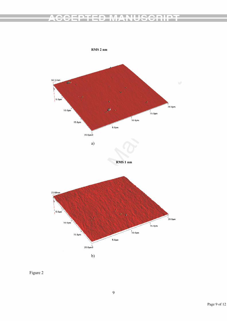
Atomic Force Microscopy studies evidenced that the rf beam addition strongly influences
the surface morphology. Thus, sample w621 prepared with RF discharge addition had a better
morphology than sample w619 deposited in the same conditions, without RF. On a 20 × 20 µm2
scale, the surface of thin films deposited by RF-PLD is more compact, without droplets and with a
smaller roughness, around 1 nm (fig. 2). Simultaneously, the RF addition results in the diminishing
of layers grain size.
The substrate temperature was also found to play an important role in the film morphology.
Even if the roughness has (small) close values for all layers, the general aspect is completely
different. A dense, droplets and cracks free film was obtained at 400 0C substrate temperature (Fig.
3b). For 200 °C substrate temperature clusters with diameter larger than 500 nm appeared on the
film surface, while at 600 0C the film became porous (fig.3).
Another parameter which influences the morphology of the thin films is laser fluence. It was
observed that decreasing the laser fluence from 8J/cm2 to 3 J/cm
2, the quality of the film surfaces
Page 2 of 12

Acc
epte
d M
anus
crip
t
3
was improved, becoming more compact, without droplets and with lower roughness and porosity
(fig. 4).
Film composition was investigated by Auger Electron Spectroscopy (AES), with an AES-
3017 spectrometer. It was noticed that for thin films grown at 200 0C and 400
0C, the ratio of atomic
concentrations W:O is almost 1:1 (the atomic concentrations of samples w83 and w91 are W
51.3%, O 48.7% and W 53.49%, O 46.51 %, respectively). Increasing the temperature to 600 0C,
the ratio of W:O became smaller (for sample w92 was recorded a W:O ratio of 38.5% : 61.5%).
This decrease can suggest the appearance of either a WO3-x compound or a WO+WO3 mixture.
The XRD patterns were recorded on a DRON DART UM-2 diffractometer equipped with a
Cu anode and a graphite monochromator in the diffracted beam in a Bragg – Brentano geometry.
Scans were acquired with a step size of 0.050 with an acquisition time on each step of 2s. Although
the X-ray patterns did not show any peak related to the formation of crystalline WOx , we can
speculate that nanocrystallites with very small dimensions are present in our layers.
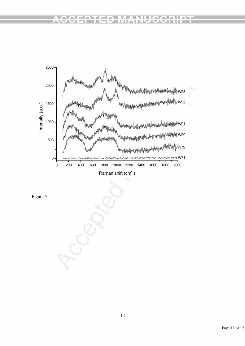
The deposited films grown on Corning glass were studied in micro-Raman configuration.
The 514 nm line of an Ar+ laser was focused on the sample by a 50x Leica Germany optical
objective (NA = 0.75 corresponding to 0.5 µm nominal spot diameter for the excitation wavelength
employed). The highest laser power used was 0.5 mW with the aim to avoid local annealing and
photo-induced structural modifications. The backscattered light was collected by the same objective
and analyzed by a Renishaw inVia Raman Microscope equipped with a holographic Notch filter
(cutoff at 100 cm-1
), a 1800 lines/mm diffraction grating and a thermoelectrically cooled RenCam
CCD detector. In fig.5 are collected the Raman spectra of all examined films. Looking at the spectra
an evolution is observed from metallic tungsten (w71) to amorphous tungsten oxide (w72),
associated to the operation of RF power. The spectrum of w72 sample is characterized by two
broad bands, the first one at low frequency in the range 100-500 cm-1
, associated to O-W-O bending
modes, and the second one at 600-1000 cm-1
, in the W-O stretching frequency range. We notice that
the latter band includes two features, the first around 800 cm-1
ascribed to W-O stretching vibration
and the second around 950 cm-1
due to W=O stretching vibration, usually associated to the
development of a nanostructure in the film [7]. These bonds are mainly located at the surface so that
an intensity increase of the corresponding band indicates a high surface to volume ratio.
Preliminary X-Ray Reflectivity measurements [8], using monochromatic x-ray source at =
0.13926 nm (CuK ) on sample w72 permitted, from the position of the critical angle c, to get a
density value of 6.48 g cm-3
, which is close to WO3 bulk density value (7.2 g cm-3
). We recall that
c is related to material density through
Page 3 of 12
Acc
epte
d M
anus
crip
t
4
21
0 '+=
A
fZrN A
c ρπ
λθ , (1)
where NA is the Avogadro’s number, r0 is the Thomson scattering length, f’ is the dispersive
correction factor, Z and A are the atomic and mass number of the material respectively.
When we move to samples w90 and w91 a separation between the two high frequency
components begins, being probably related to the higher substrate temperature (400°C) in both
films. The increased RF power at which sample w91 was deposited does not significantly affect the
features of Raman spectrum. The spectra of samples w92 and w95 show a definite trend towards
crystallization, as evidenced by a progressive definition of the W-O stretching bands at about 800
cm-1
. The dramatic role of substrate temperature Ts is highlighted by comparing the spectra of
samples w91 (Ts, 400°C) and w92 (Ts, 600°C). When we compare the spectra of sample w91 and
w95 the effect of laser fluence emerges. Decreasing the laser fluence, results in increased film
crystallinity with a similar effect to increasing Ts. In fact a lower fluence coincides with a reduced
plume expansion, in turn favoring cluster synthesis in the plume during its flight.
Conclusions
We have demonstrated the growth of WOx layers with high WO3 content by radiofrequency
assisted pulsed laser deposition. Parameters like temperature and laser fluence have a big impact on
film crystallinity and roughness. It was observed that the decrease of the laser fluence results in
increased film crystallinity with a similar effect while increasing the substrate temperature.
Nevertheless, the use of a higher temperature (600°C) leads to the appearance of pores on the film’s
surface. Under the investigated experimental conditions, the best WOx films were obtained on
Corning glass at 3 J/cm2, 400
0C and 150 W power of RF discharge. Controlling the experimental
parameters a nanocrystalline structure, an amorphous layer or an uniform and compact layer with
large grains (180 nm-200 nm) can be obtained.
Page 4 of 12

Acc
epte
d M
anus
crip
t
5
References:
[1] Ashirt P V, Bader G and Truong V-V 1998 Thin Solid Films, 320 324
[2] Xu Z, Vetelino J F, Lec R and Parker D C 1990 J. Vac. Sci.,Technol. A 8 3634
[3] Tagtstrom P and Jansson U 1999 Thin Solid Films 352, 107
[4] Haro-Poniaowski E, Jouanne M and Morhange J F 1998 Appl. Surf. Sci. 127–9 674
[5] Lee S H, Cheong H M, Edwin C, Pitts J R and Deb S K 2000, Appl. Phys. Lett. 76 3908
[6] G. Dinescu, B.Mitu, E. Aldea, M. Dinescu, Vacuum, 56, (2000), 83
[7] M. Boulova and G. Lucazeau, J. Sol. St. Chem., 167 (2002) 425
[8] V. Holy, U. Pietsch, T. Baumbach, Springer, Berlin, (1999)
Page 5 of 12
Acc
epte
d M
anus
crip
t
6
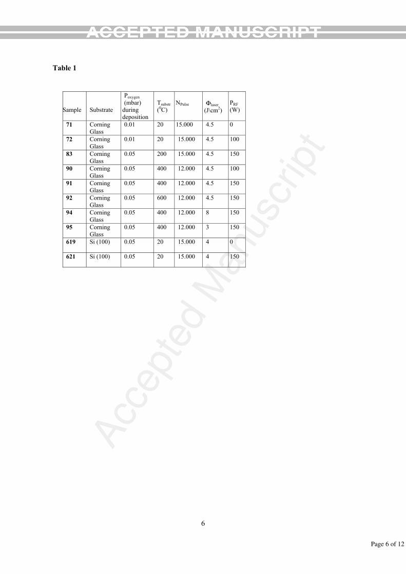
Table 1
Sample Substrate
Poxygen
(mbar)
during
deposition
Tsubstr
(0C)
NPulse Φlaser
(J\cm2)
PRF
(W)
71 Corning
Glass
0.01 20 15.000 4.5 0
72 Corning
Glass
0.01 20 15.000 4.5 100
83 Corning
Glass
0.05 200 15.000 4.5 150
90 Corning
Glass
0.05 400 12.000 4.5 100
91 Corning
Glass
0.05 400 12.000 4.5 150
92 Corning
Glass
0.05 600 12.000 4.5 150
94 Corning
Glass
0.05 400 12.000 8 150
95 Corning
Glass
0.05 400 12.000 3 150
619 Si (100) 0.05 20 15.000 4 0
621 Si (100) 0.05 20 15.000 4 150
Page 6 of 12

Acc
epte
d M
anus
crip
t
7
Figure captions:
Fig.1 The PLD-RF system used to obtain thin films of WOx
Fig.2 AFM images for sample deposited in the same condition but with different RF power a) 0 W
and b) 150 W
Fig. 3 AFM images for samples deposited in the same conditions but at different temperatures a)
2000C, b) 400
0C and c) 600
0C
Fig. 4 AFM images for sample deposited in the same conditions but with different laser fluences a)
8.28 J/cm2, b) 4.5 J/cm
2, c) 3 J/cm
2
Fig. 5 Raman spectra for samples w71, w72, w90, w91, w92, w95
Page 7 of 12

Acc
epte
d M
anus
crip
t
8
Gas inlet
Water coolingRF supply
Stainless steelvacuum chamber
Target
Substrate
RF plasmasource
LASERplasma
RF plasmabeam
Focusinglens
LASERbeam
Figure 1
Page 8 of 12
Acc
epte
d M
anus
crip
t
9
RMS 2 nm
a)
RMS 1 nm
b)
Figure 2
Page 9 of 12

Acc
epte
d M
anus
crip
t
10
RMS 5.5 nm RMS 3.5 nm
a) b)
RMS 5.1 nm
c)
Figure 3
Page 10 of 12

Acc
epte
d M
anus
crip
t
11
RMS 7 nm RMS 4.4 nm
a) b)
RMS 2.3 nm
c)
Figure 4
Page 11 of 12
Acc
epte
d M
anus
crip
t
12
Figure 5
0 200 400 600 800 1000 1200 1400 1600 1800 2000
0
500
1000
1500
2000
2500
W95
W92
W91
W90
W72
W71
Inte
nsity (
a.u
.)
Raman shift (cm-1)
Page 12 of 12