rl78/g13 self-programming (received data via uart) · rl78/g13 self-programming (uart)...
TRANSCRIPT
APPLICATION NOTE
R01AN1356EJ0110 Rev. 1.10 Page 1 of 50
June 01, 2016
RL78/G13 Self-Programming (Received Data via UART)
Introduction
This application note gives the outline of flash memory reprogramming using a self-programming technique. In this application note, flash memory is reprogrammed using the flash memory self-programming library Type01.
The sample program described in this application note limits the target of reprogramming to the boot area. For details on the procedures for performing self-programming and for reprogramming the entire area of code flash memory, refer to RL78/G13 Microcontroller Flash Memory Self-Programming Execution (R01AN0718E) Application Note.
Target Device
RL78/G13
When applying the sample program covered in this application note to another microcomputer, modify the program according to the specifications for the target microcomputer and conduct an extensive evaluation of the modified program.
R01AN1356EJ0110Rev. 1.10
June 01, 2016
RL78/G13 Self-Programming (UART)
R01AN1356EJ0110 Rev. 1.10 Page 2 of 50
June 01, 2016
Contents
1. Specifications ...................................................................................................................................... 4 1.1 Outline of the Flash Memory Self-Programming Library ......................................................................... 4 1.2 Code Flash Memory ............................................................................................................................. 5 1.3 Flash Memory Self-Programming ......................................................................................................... 7 1.3.1 Boot Swap Function ........................................................................................................................... 7 1.3.2 Flash Memory Reprogramming ........................................................................................................... 9 1.3.3 Flash Shield Window........................................................................................................................ 10
1.4 How to Get the Flash Memory Self-Programming Library..................................................................... 11
2. Operation Check Conditions ............................................................................................................... 11
3. Related Application Notes .................................................................................................................. 12
4. Description of the Hardware ............................................................................................................... 13 4.1 Hardware Configuration Example ....................................................................................................... 13 4.2 List of Pins to be Used ....................................................................................................................... 14
5. Description of the Software ................................................................................................................ 15 5.1 Communication Specifications ............................................................................................................ 15 5.1.1 START Command ........................................................................................................................... 15 5.1.2 WRITE Command ........................................................................................................................... 15 5.1.3 END Command ............................................................................................................................... 15 5.1.4 Communication Sequence ................................................................................................................. 16
5.2 Operation Outline .............................................................................................................................. 17 5.3 File Configuration .............................................................................................................................. 19 5.4 List of Option Byte Settings ................................................................................................................ 20 5.5 On-chip Debug Security ID ................................................................................................................ 20 5.6 Link Directive File ............................................................................................................................. 21 5.7 List of Constants ................................................................................................................................ 22 5.8 List of Functions ................................................................................................................................ 22 5.9 Function Specifications ...................................................................................................................... 23 5.10 Flowcharts ........................................................................................................................................ 26 5.10.1 Initialization Function ..................................................................................................................... 27 5.10.2 System Initialization Function ......................................................................................................... 28 5.10.3 I/O Port Setup ................................................................................................................................ 29 5.10.4 CPU Clock Setup ........................................................................................................................... 30 5.10.5 SAU0 Setup ................................................................................................................................... 31 5.10.6 UART1 Setup ................................................................................................................................ 32 5.10.7 Main Processing ............................................................................................................................. 35 5.10.8 Starting the UART1 ........................................................................................................................ 37 5.10.9 Data Reception via UART1 ............................................................................................................. 38 5.10.10 Receive Packet Analysis ............................................................................................................... 40 5.10.11 Flash Memory Self-Programming Execution ................................................................................... 41 5.10.12 Flash Memory Self-Programming Initialization ............................................................................... 42 5.10.13 Flash Memory Reprogramming Execution ...................................................................................... 44 5.10.14 Data Transmission via UART1 ...................................................................................................... 47
RL78/G13 Self-Programming (UART)
R01AN1356EJ0110 Rev. 1.10 Page 3 of 50
June 01, 2016
5.11 Operation Check Procedure ................................................................................................................ 48 5.11.1 Making Checks with a Debugger ..................................................................................................... 48
6. Sample Code ..................................................................................................................................... 50
7. Documents for Reference ................................................................................................................... 50

RL78/G13 Self-Programming (UART)
R01AN1356EJ0110 Rev. 1.10 Page 4 of 50
June 01, 2016
1. Specifications
This application note explains a sample program that performs flash memory reprogramming using a self-programming library.
The sample program displays the information about the current version of the library on the LCD. Subsequently, the program receives data (reprogramming data) from the sending side and, after turning on the LED indicating that it is accessing flash memory, carries out self-programming to rewrite the code flash memory with the reprogramming data. When the rewrite is completed, the sample program turns off the LED and displays the information about the new version on the LCD.
Table 1.1 lists the peripheral functions to be used and their uses.
Table 1.1 Peripheral Functions to be Used and their Uses
Peripheral Function Use
Channel 2 of serial array unit 0 Receives data via UART.
Channel 3 of serial array unit 0 Sends data via UART.
Port I/O Displays text on the LCD.
Turns on and off the LED.
1.1 Outline of the Flash Memory Self-Programming Library The flash memory self-programming library is a software product that is used to reprogram the data in the code flash memory using the firmware installed on the RL78 microcontroller.
The contents of the code flash memory can be reprogrammed by calling the flash memory self-programming library from a user program.
To do flash memory self-programming, it is necessary for the user program to perform initialization for flash memory self -programming and to execute the C or assembler functions that correspond to the library functions to be used.
RL78/G13 Self-Programming (UART)
R01AN1356EJ0110 Rev. 1.10 Page 5 of 50
June 01, 2016
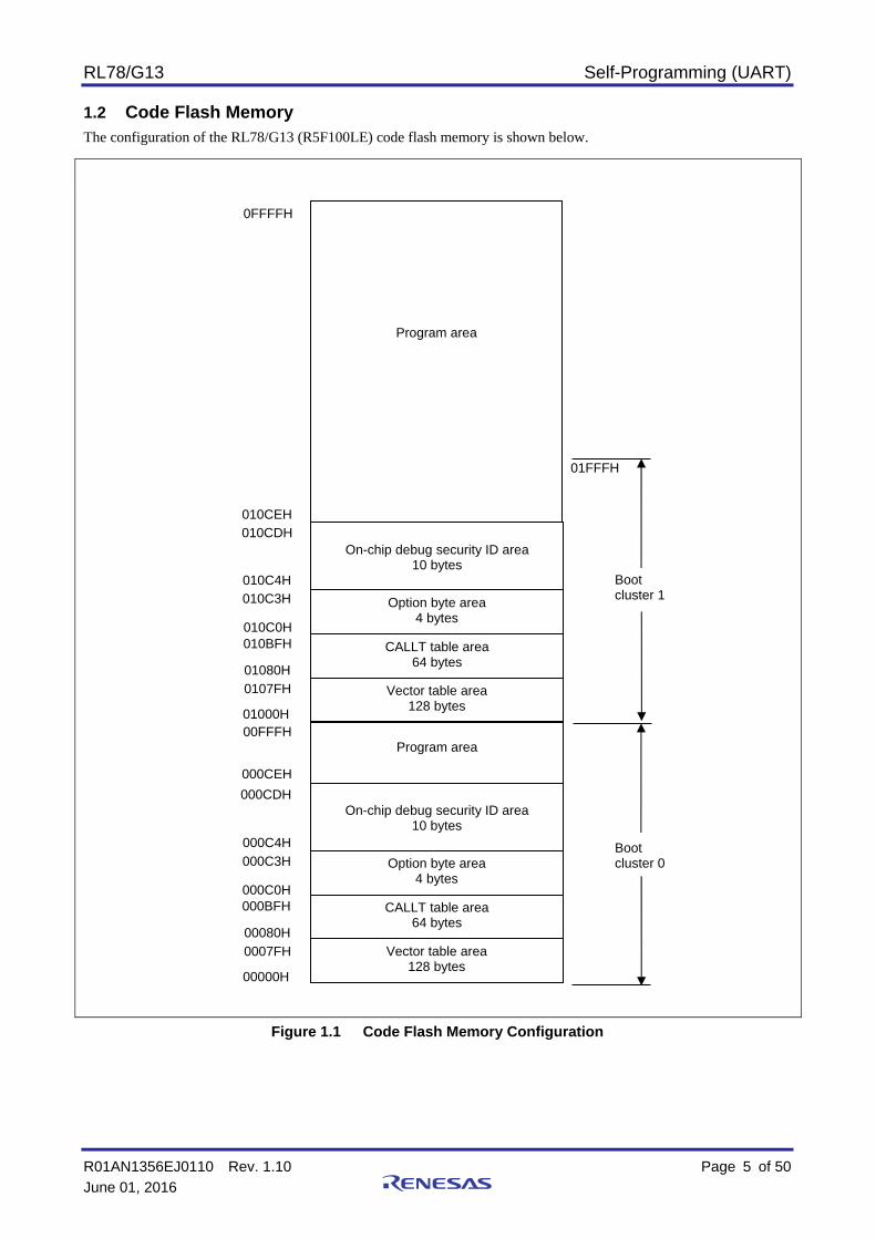
1.2 Code Flash Memory The configuration of the RL78/G13 (R5F100LE) code flash memory is shown below.
Figure 1.1 Code Flash Memory Configuration
Vector table area 128 bytes
Boot cluster 0
CALLT table area 64 bytes
Option byte area 4 bytes
On-chip debug security ID area 10 bytes
Program area
Vector table area 128 bytes
CALLT table area 64 bytes
Option byte area 4 bytes
On-chip debug security ID area 10 bytes
Program area
00000H
0007FH
00080H
000BFH 000C0H
000C3H
000C4H
000CDH
000CEH
00FFFH 01000H
0107FH
01080H
010BFH 010C0H
010C3H 010C4H
010CDH 010CEH
0FFFFH
Boot cluster 1
01FFFH

RL78/G13 Self-Programming (UART)
R01AN1356EJ0110 Rev. 1.10 Page 6 of 50
June 01, 2016
Caution: When the boot swap function is used, the option byte area (000C0H to 000C3H) in boot cluster 0 is swapped with the option byte area (010C0H to 010C3H) in boot cluster 1. Accordingly, place the same values in the area (010C0H to 010C3H) as those in the area (000C0H to 000C3H) when using the boot swap function.
The features of the RL78/G13 code flash memory are summarized below.
Table 1.2 Features of the Code Flash Memory
Item Description
Minimum unit of erasure and verification
1 block (1024 bytes)
Minimum unit of programming 1 word (4 bytes)
Security functions
Block erasure, programming, and boot area reprogramming protection are supported.
(They are enabled at shipment)
It is possible to disable reprogramming and erasure outside the specified window only at flash memory self-programming time using the flash shield window.
Security settings programmable using the flash memory self-programming library
Caution: The boot area reprogramming protection setting and the security settings for outside the flash shield window are disabled during flash memory self-programming.

RL78/G13 Self-Programming (UART)
R01AN1356EJ0110 Rev. 1.10 Page 7 of 50
June 01, 2016
1.3 Flash Memory Self-Programming The RL78/G13 is provided with a library for flash memory self-programming. Flash memory self-programming is accomplished by calling functions of the flash memory self-programming library from the reprogramming program.
The flash memory self-programming library for the RL78/G13 controls flash memory reprogramming using a sequencer (a dedicated circuit for controlling flash memory). The code flash memory cannot be referenced while control by the sequencer is in progress. When the user program needs to be run while the sequencer control is in progress, therefore, it is necessary to relocate part of the segments for the flash memory self-programming library and the reprogramming program in RAM when erasing or reprogramming the code flash memory or making settings for the security flags. If there is no need to run the user program while the sequencer control is in progress, it is possible to keep the flash memory self-programming library and reprogramming program on ROM (code flash memory) for execution.
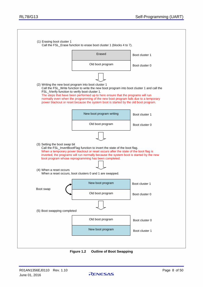
1.3.1 Boot Swap Function When reprogramming of the area where vector table data, the basic functions of the program, and flash memory self-programming library are allocated fails due to a temporary power blackout or a reset caused by an external factor, the data that is being reprogrammed will be corrupted, as the result of which the restarting of the user program or reprogramming cannot be accomplished when a reset is subsequently performed. This problem is be avoided by the introduction of the boot swap function.
The boot swap function swaps between boot cluster 0 which is the boot program area and boot cluster 1 which is the target of boot swapping. A new program is written into boot cluster 1 before reprogramming is attempted. This boot cluster 1 is swapped with boot cluster 0 and boot cluster 1 is designated as the boot program area. In this configuration, even when a temporary power blackout occurs while the boot program area is being reprogrammed, the system boot will start at boot cluster 1 on the next reset start, thus ensuring the normal execution of the programs.
The outline image of boot swapping is shown in the figure below.
RL78/G13 Self-Programming (UART)
R01AN1356EJ0110 Rev. 1.10 Page 8 of 50
June 01, 2016
Figure 1.2 Outline of Boot Swapping
Boot cluster 1 Erased
Old boot program Boot cluster 0
(1) Erasing boot cluster 1 Call the FSL_Erase function to erase boot cluster 1 (blocks 4 to 7).
Boot cluster 1 New boot program writing
Old boot program Boot cluster 0
(2) Writing the new boot program into boot cluster 1 Call the FSL_Write function to write the new boot program into boot cluster 1 and call the FSL_IVerify function to verify boot cluster 1. The steps that have been performed up to here ensure that the programs will run normally even when the programming of the new boot program fails due to a temporary power blackout or reset because the system boot is started by the old boot program.
Boot cluster 1 New boot program
Old boot program Boot cluster 0
Boot swap
(3) Setting the boot swap bit Call the FSL_InvertBootFlag function to invert the state of the boot flag. When a temporary power blackout or reset occurs after the state of the boot flag is inverted, the programs will run normally because the system boot is started by the new boot program whose reprogramming has been completed.
(4) When a reset occurs When a reset occurs, boot clusters 0 and 1 are swapped.
Boot cluster 0 Old boot program
New boot program Boot cluster 1
(5) Boot swapping completed

RL78/G13 Self-Programming (UART)
R01AN1356EJ0110 Rev. 1.10 Page 9 of 50
June 01, 2016
1.3.2 Flash Memory Reprogramming This subsection describes the outline image of reprogramming using the flash memory self-programming technique. The program that performs flash memory self-programming is placed in boot cluster 0.
The sample program covered in this application note limits the target of reprogramming to the boot area. For details on the procedures for perform self-programming and for reprogramming the entire area of code flash memory, refer to RL78/G13 Microcontroller Flash Memory Self-Programming Execution (R01AN0718E) Application Note.
Figure 1.3 Outline of Flash Memory Reprogramming (1/2)
Boot cluster 1
Boot program Boot cluster 0
User program
(1) Erasing the block to be reprogrammed
00000H
00FFFH 01000H
01FFFH 02000H
0FFFFH
Erase
Boot cluster 1
Boot program Boot cluster 0
User program
(2) Writing and verifying the block to be reprogrammed
00000H
00FFFH 01000H
01FFFH 02000H
0FFFFH
Write
(3) Repeat the cycle of erasing, writing, and verifying the block up to the last block.
Boot cluster 1 New boot program
Boot program Boot cluster 0
New user program
00000H
00FFFH
01000H
01FFFH 02000H
0FFFFH
RL78/G13 Self-Programming (UART)
R01AN1356EJ0110 Rev. 1.10 Page 10 of 50
June 01, 2016
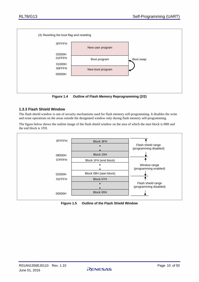
Figure 1.4 Outline of Flash Memory Reprogramming (2/2)
1.3.3 Flash Shield Window The flash shield window is one of security mechanisms used for flash memory self-programming. It disables the write and erase operations on the areas outside the designated window only during flash memory self-programming.
The figure below shows the outline image of the flash shield window on the area of which the start block is 08H and the end block is 1FH.
Figure 1.5 Outline of the Flash Shield Window
Block 07H
Block 00H 00000H
01FFFH
Block 1FH (end block)
Block 08H (start block) 02000H
07FFFH
Block 3FH
Block 20H 08000H
0FFFFH
Flash shield range (programming disabled)
Flash shield range (programming disabled)
Window range (programming enabled)
(4) Rewriting the boot flag and resetting
New boot program
Boot program
New user program
00000H
00FFFH 01000H
01FFFH 02000H
0FFFFH
Boot swap

RL78/G13 Self-Programming (UART)
R01AN1356EJ0110 Rev. 1.10 Page 11 of 50
June 01, 2016
1.4 How to Get the Flash Memory Self-Programming Library Before compiling the sample program, please download the latest flash self-programming library and copy the library files to the following folder below ”Workspace”.
incrl78 folder : fsl.h, fsl.inc, fsl_types.h
librl78 folder : fsl.lib
The flash memory self-programming library is available on the Renesas Electronics Website.
Please contact your local Renesas Electronics sales office or distributor for more information.
2. Operation Check Conditions
The sample code described in this application note has been checked under the conditions listed in the table below.
Table 2.1 Operation Check Conditions
Item Description
Microcontroller used RL78/G13 (R5F100LEA)
Operating frequency High-speed on-chip oscillator (HOCO) clock: 32 MHz
CPU/peripheral hardware clock: 32 MHz
Operating voltage 5.0 V (Operation is possible over a voltage range of 2.9 V to 5.5 V.)
LVD operation (VLVD): Reset mode which uses 2.81 V (2.76 V to 2.87 V)
Integrated development environment CS+ V3.02.00 from Renesas Electronics Corp.
C compiler CA78K0R V1.72 from Renesas Electronics Corp.
Board to be used Renesas Starter Kit for RL78/G13 (R0K50100LS000BE)
Flash memory self-programming library
(Type, Ver)
FSLRL78 Type01, Ver 2.20 Note
Note: Use and evaluate the latest version.
RL78/G13 Self-Programming (UART)
R01AN1356EJ0110 Rev. 1.10 Page 12 of 50
June 01, 2016
3. Related Application Notes
The application notes that are related to this application note are listed below for reference.
RL78/G13 Initialization (R01AN0451E) Application Note RL78/G13 Serial Array Unit (UART Communication) (R01AN0459E) Application Note RL78 Microcontroller Flash Memory Self-Programming Library Type01 (R01AN0350E) Application Note

RL78/G13 Self-Programming (UART)
R01AN1356EJ0110 Rev. 1.10 Page 13 of 50
June 01, 2016
4. Description of the Hardware
4.1 Hardware Configuration Example Figure 4.1 shows an example of the hardware configuration used for this application note.
Figure 4.1 Hardware Configuration
Cautions: 1. The purpose of this circuit is only to provide the connection outline and the circuit is simplified accordingly. When designing and implementing an actual circuit, provide proper pin treatment and make sure that the hardware's electrical specifications are met (connect the input-only ports separately to VDD or VSS via a resistor).
2. VDD must be held at not lower than the reset release voltage (VLVD) that is specified as LVD.
RES (implemented on the CPU board)
For on-chip debugger
P52
RESET
VDD
RL78/G13
EVDD
EVDD
VDD
EVSS
VSS
REGC
P40/TOOL0
P02/TxD0
VDD
R0K50100LS000BE
Sending side (sending reprogramming
data)
P70
P71
P72
P73P54
P55
Debug LCD
LED0
EVDD
P03/RxD0

RL78/G13 Self-Programming (UART)
R01AN1356EJ0110 Rev. 1.10 Page 14 of 50
June 01, 2016
4.2 List of Pins to be Used Table 4.1 lists pins to be used and their functions.
Table 4.1 Pins to be Used and their Functions
Pin Name I/O Description
P02/ANI17/SO10/TxD1 Output UART serial data transmit pin
P03/ANI16/SI10/RxD1/SDA10 Input UART serial data receive pin
P52 Output LED0 (indicating flash memory access status) on/off control
P54 Output Debug LCD control
P55 Output Debug LCD control
P70/KR0/SCK21/SCL21 Output Debug LCD control
P71/KR1/SI21/SDA21 Output Debug LCD control
P72/KR2/SO21 Output Debug LCD control
P73/KR3/SO01 Output Debug LCD control

RL78/G13 Self-Programming (UART)
R01AN1356EJ0110 Rev. 1.10 Page 15 of 50
June 01, 2016
5. Description of the Software
5.1 Communication Specifications The sample program covered in this application note receives reprogramming data via the UART bus for flash memory self-programming. The sending side sends three commands, i.e., the START, WRITE, and END commands. The sample program takes actions according to the command it received, and, if the command terminates normally, returns a normal response (0x01) to the sending side. If the command terminates abnormally, the program returns no response, displays "ERROR!" on the LCD, and suppresses the execution of the subsequent operations. This section describes the necessary UART communication settings and the specifications for the commands.
Table 5.1 UART Communication Settings
Data bit length [bit] 8
Data transfer direction LSB first
Parity setting No parity
Transfer rate [bps] 115200
5.1.1 START Command When the sample program receives the START command, it performs initialization processing for flash memory self-programming. When the command terminates normally, the program returns a normal response (0x01) to the sending side. In the case of an abnormal termination, the sample program returns no response, displays "ERROR!" on the LCD, and suppresses the execution of the subsequent operations.
5.1.2 WRITE Command When the sample program receives the WRITE command, it writes the data it received into flash memory, and performs verify processing each time it completes the write of one block. The sample program returns a normal response (0x01) to the sending side on normal termination of the command. In the case of an abnormal termination, the sample program returns no response, displays "ERROR!" on the LCD, and suppresses the execution of the subsequent operations.
5.1.3 END Command When the sample program receives the END command, it performs verify processing on the block that is currently being written. If the verification terminates normally, the program inverts the state of the boot flag, then generates a reset for boot swapping. In the case of an abnormal termination, the sample program displays "ERROR!" on the LCD and suppresses the execution of the subsequent operations. When the sample program receives the END command, it returns no response to the sending side whether the command terminates normally or abnormally.
* The checksum is the sum of the command and data fields in units of bytes.
START code (0x01)
Data length (0x0002)
Command (0x02)
Data (None)
Checksum (1 byte)
START code (0x01)
Data length (0x0102)
Command (0x03)
Data (256 bytes)
Checksum (1 byte)
START code (0x01)
Data length (0x0002)
Command (0x04)
Data (None)
Checksum (1 byte)

RL78/G13 Self-Programming (UART)
R01AN1356EJ0110 Rev. 1.10 Page 16 of 50
June 01, 2016
5.1.4 Communication Sequence This sample program takes actions according to the sequence described below upon receipt of a command from the sending side.
(1) Sending side:
Sends the START command.
(2) Sample program:
Turns on LED1 which indicates that flash memory is being accessed, performs initialization for flash memory self-programming, and returns a normal response (0x01) upon normal termination.
(3) Sending side:
Sends the WRITE command and reprogramming data (256 bytes).
(4) Sample program:
Writes the data it received into the code flash memory. The write address starts at 0x1000 (start of boot cluster 1). Subsequently, it is incremented by the receive data size (size of reprogramming data: 256 bytes) each time the sample program receives the WRITE command and reprogramming data.
The program performs verify processing when the rewrite of 1 block (1024 bytes) is completed.
When all of these steps terminate normally, the sample program returns a response (0x01).
(5) Steps (3) and (4) are repeated until the reprogramming of all data is completed.
(6) Sending side:
Sends the END command.
(7) Sample program:
Performs verify processing on the block that is currently subjected to reprogramming. The sample program then inverts the state of the boot flag, and generates a reset after turning off LED0 which indicates that flash memory is being accessed.
RL78/G13 Self-Programming (UART)
R01AN1356EJ0110 Rev. 1.10 Page 17 of 50
June 01, 2016
5.2 Operation Outline This application note explains a sample program that performs flash memory reprogramming using a self-programming library.
The sample program displays the information about the current version of the library on the LCD. Subsequently, the program receives data (reprogramming data) from the sending side and, after turning on the LED indicating that it is accessing flash memory, carries out self-programming to rewrite the code flash memory with the reprogramming data. When reprogramming is completed, the sample program turns off the LED and displays the information about the new version on the LCD.
(1) Initializes the SAU0 channels 2 and 3.
<Setting conditions>
Uses the SAU0 channels 2 and 3 as UART. Uses the P02/TxD1 pin for data output and the P03/RxD1 pin for data input. Sets the data length to 8 bits. Sets the order of data transfer mode to LSB first. Sets the parity setting to “No parity”. Sets the receive data level to standard. Sets the transfer rate to 115200 bps. (2) Sets up the I/O port.
<Setting conditions>
LED on/off control port (LED0): Sets P52 for output. (3) Disables interrupts.
(4) Starts the UART1.
(5) Initializes the LCD and displays on the LCD the string that is set to the constant LCD_STRING.
(6) Enters the HALT mode and waits for data from the sending side.
Switches into the normal operation mode from the HALT mode upon a UART receive end interrupt request.

RL78/G13 Self-Programming (UART)
R01AN1356EJ0110 Rev. 1.10 Page 18 of 50
June 01, 2016
(7) Upon receipt of a START command (0x02) from the sending side, performs initialization for self-programming.
Sets P52 to the low level and turns on LED0 indicating that flash memory is being accessed. Calls the FSL_Init function to initialize the flash memory self-programming environment and makes the following
settings: Voltage mode : Full-speed mode CPU operating frequency : 32 [MHz] Status check mode : Status check internal mode
Calls the FSL_Open function to start flash memory self-programming (starting the flash memory environment). Calls the FSL_PrepareFunctions function to make available the flash memory functions (standard reprogramming
functions) that are necessary for the RAM executive. Calls the FSL_PrepareExtFunctions function to make available the flash memory functions (extended functions)
that are necessary for the RAM executive. Calls the FSL_GetFlashShieldWindow function to get the start and end blocks of the flash shield window. If the start block of the flash shield window is a block other than block 0 or if the end block is a block other than
block 63, calls the FSL_SetFlashShieldWindow function to set the start block of the flash shield window to block 0 and the end block to block 63.
(8) Sets the write destination address to 0x1000 (start of boot cluster 1).
(9) Sends a normal response (0x01) to the sending side.
(10) Receives the WRITE command (0x03) and reprogramming data (256 bytes).
(11) Computes the reprogramming target block from the write destination address.
(12) Calls the FSL_BlankCheck function to check whether the reprogramming target block has already been reprogrammed.
(13) If the reprogramming target block is reprogrammed, calls the FSL_Erase function to erase the reprogramming target block.
(14) Calls the FSL_Write function to write the received data at the write destination address.
(15) Adds the write size to the write destination address.
(16) Sends a normal response (0x01) to the sending side.
(17) Receives the WRITE command and reprogramming data (256 bytes) or the END command (0x04).
(18) Repeats steps (14) to (17) until 1 block (1024 bytes) of programming is completed or an END command (0x04) is received from the sending side. Proceeds with the next step when 1 block 1024 bytes) of programming is completed or an END command (0x04) is received from the sending side.
(19) Calls the FSL_IVerify function to verify the reprogramming target block.
(20) Repeats steps (11) to (19) unless an END command (0x04) is received from the sending side. Proceeds with the next step when an END command is received.
(21) Calls the FSL_InvertBootFlag function to invert the state of the boot flag. Boot clusters 0 and 1 will then be swapped at reset time.
(22) Sets P52 to the high level, turns off LED0 indicating that flash memory is being accessed, then calls the FSL_ForceReset function to generate an internal reset.
Caution: When flash memory self-programming could not be terminated normally (error occurring during processing), the sample program displays "ERROR!" on the LCD and suppresses the execution of the subsequent operations.
RL78/G13 Self-Programming (UART)
R01AN1356EJ0110 Rev. 1.10 Page 19 of 50
June 01, 2016
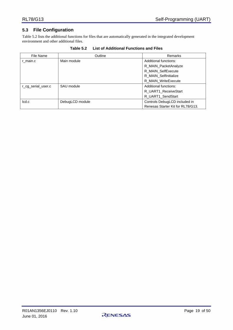
5.3 File Configuration Table 5.2 lists the additional functions for files that are automatically generated in the integrated development environment and other additional files.
Table 5.2 List of Additional Functions and Files
File Name Outline Remarks
r_main.c Main module Additional functions:
R_MAIN_PacketAnalyze
R_MAIN_SelfExecute R_MAIN_SelfInitialize
R_MAIN_WriteExecute
r_cg_serial_user.c SAU module
Additional functions:
R_UART1_ReceiveStart
R_UART1_SendStart
lcd.c DebugLCD module Controls DebugLCD included in Renesas Starter Kit for RL78/G13.
RL78/G13 Self-Programming (UART)
R01AN1356EJ0110 Rev. 1.10 Page 20 of 50
June 01, 2016
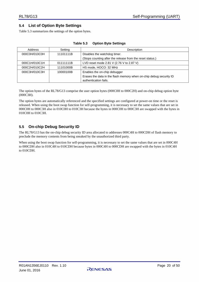
5.4 List of Option Byte Settings Table 5.3 summarizes the settings of the option bytes.
Table 5.3 Option Byte Settings
Address Setting Description
000C0H/010C0H 11101111B Disables the watchdog timer.
(Stops counting after the release from the reset status.)
000C1H/010C1H 01111111B LVD reset mode 2.81 V (2.76 V to 2.87 V)
000C2H/010C2H 11101000B HS mode, HOCO: 32 MHz
000C3H/010C3H 10000100B Enables the on-chip debugger
Erases the data in the flash memory when on-chip debug security ID authentication fails.
The option bytes of the RL78/G13 comprise the user option bytes (000C0H to 000C2H) and on-chip debug option byte (000C3H).
The option bytes are automatically referenced and the specified settings are configured at power-on time or the reset is released. When using the boot swap function for self-programming, it is necessary to set the same values that are set in 000C0H to 000C3H also in 010C0H to 010C3H because the bytes in 000C0H to 000C3H are swapped with the bytes in 010C0H to 010C3H.
5.5 On-chip Debug Security ID The RL78/G13 has the on-chip debug security ID area allocated to addresses 000C4H to 000CDH of flash memory to preclude the memory contents from being sneaked by the unauthorized third party.
When using the boot swap function for self-programming, it is necessary to set the same values that are set in 000C4H to 000CDH also in 010C4H to 010CDH because bytes in 000C4H to 000CDH are swapped with the bytes in 010C4H to 010CDH.

RL78/G13 Self-Programming (UART)
R01AN1356EJ0110 Rev. 1.10 Page 21 of 50
June 01, 2016
;*********************************************************** ; Redefined ROM area ;*********************************************************** ; ---------------------------------------------------------- ; Define new memory entry for boot cluster 0 ; ---------------------------------------------------------- MEMORY ROM : ( 000000H, 001000H ) ; ---------------------------------------------------------- ; Define new memory entry for write-data area ; ---------------------------------------------------------- MEMORY OCDROM : ( 00FE00H, 000200H ) ;*********************************************************** ; Library(fsl.lib) segment ;*********************************************************** ; ---------------------------------------------------------- ; Merge FSL_FCD segment ; ---------------------------------------------------------- MERGE FSL_FCD := ROM ; ---------------------------------------------------------- ; Merge FSL_FECD segment ; ---------------------------------------------------------- MERGE FSL_FECD := ROM ; ---------------------------------------------------------- ; Merge FSL_RCD segment ; ---------------------------------------------------------- MERGE FSL_RCD := ROM ; ---------------------------------------------------------- ; Merge FSL_BCD segment ; ---------------------------------------------------------- MERGE FSL_BCD := ROM ; ---------------------------------------------------------- ; Merge FSL_BECD segment ; ---------------------------------------------------------- MERGE FSL_BECD := ROM ;*********************************************************** ; Redefined RAM area ;*********************************************************** ; ---------------------------------------------------------- ; Define new memory entry for self-RAM ; ---------------------------------------------------------- MEMORY SELFRAM : ( 0FEF00H, 00040AH ) ; ---------------------------------------------------------- ; Redefined default data segment RAM ; ---------------------------------------------------------- MEMORY RAM : ( 0FF30AH, 000B16H ) ; ---------------------------------------------------------- ; Define new memory entry for saddr area ; ---------------------------------------------------------- MEMORY RAM_SADDR : ( 0FFE20H, 0001E0H ) ;*********************************************************** ; run-time library segment ( 0000H - FFFFH ) ;*********************************************************** ; ---------------------------------------------------------- ; Merge @@LCODE,@@LCODEL(run-time library) segment ; ---------------------------------------------------------- MERGE @@LCODE := ROM MERGE @@LCODEL := ROM ;*********************************************************** ; const segment ;*********************************************************** MERGE CNST_SEG := ROM
5.6 Link Directive File The reprogramming program that performs flash memory self-programming and the flash memory self-programming library are allocated to blocks 0 to 3 (boot cluster 0) by the link directive file. It is also used to make configuration so that the RAM area to be used by the flash memory self-programming library will not be used.
The outline of the link directive file that this sample program uses is shown below.
Code area definition The code is allocated to the boot area.
OCD monitor area definition
Allocates the flash memory self-programming library to the boot area.
Defines so that the area to be used by the flash memory self-programming library will not be used as the standard RAM area.
Standard RAM area definition
Defines so that the area to be used by the flash memory self-programming library will not be used as the standard RAM area.
Allocates the run-time library to the boot area.
Allocates the const variable to the boot area.
RL78/G13 Self-Programming (UART)
R01AN1356EJ0110 Rev. 1.10 Page 22 of 50
June 01, 2016
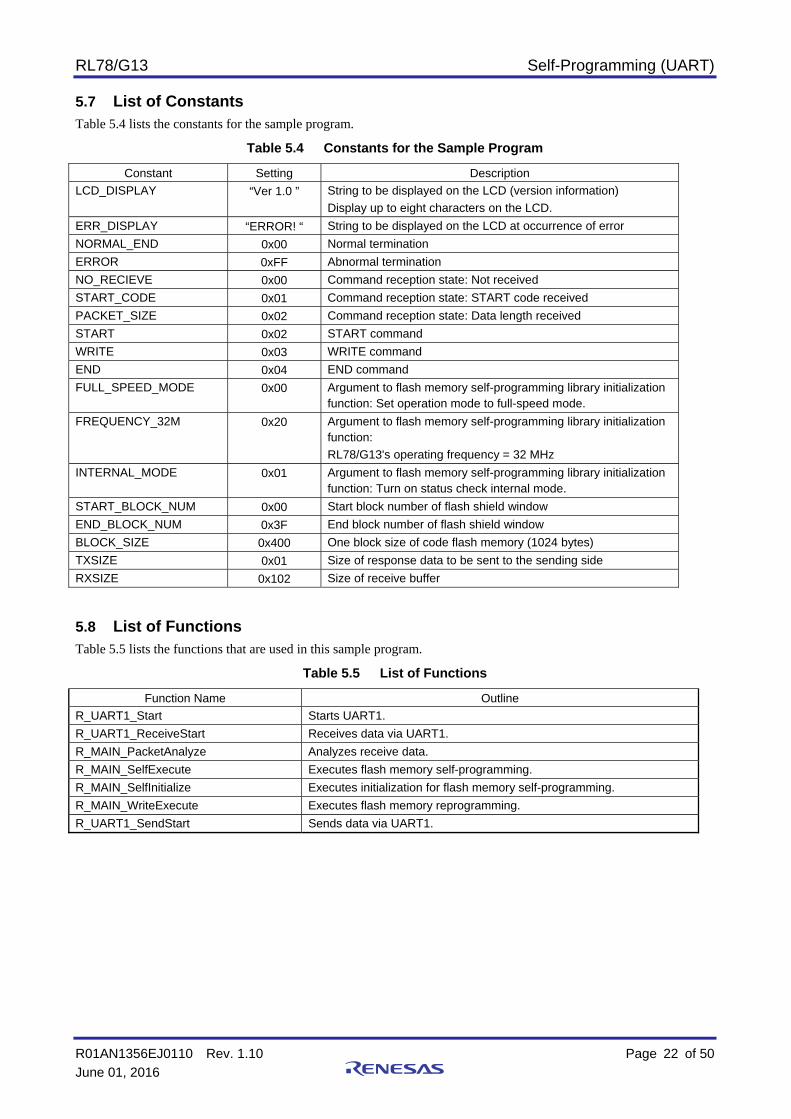
5.7 List of Constants Table 5.4 lists the constants for the sample program.
Table 5.4 Constants for the Sample Program
Constant Setting Description
LCD_DISPLAY “Ver 1.0 ” String to be displayed on the LCD (version information)
Display up to eight characters on the LCD.
ERR_DISPLAY “ERROR! “ String to be displayed on the LCD at occurrence of error
NORMAL_END 0x00 Normal termination
ERROR 0xFF Abnormal termination
NO_RECIEVE 0x00 Command reception state: Not received
START_CODE 0x01 Command reception state: START code received
PACKET_SIZE 0x02 Command reception state: Data length received
START 0x02 START command
WRITE 0x03 WRITE command
END 0x04 END command
FULL_SPEED_MODE 0x00 Argument to flash memory self-programming library initialization function: Set operation mode to full-speed mode.
FREQUENCY_32M 0x20 Argument to flash memory self-programming library initialization function:
RL78/G13's operating frequency = 32 MHz
INTERNAL_MODE 0x01 Argument to flash memory self-programming library initialization function: Turn on status check internal mode.
START_BLOCK_NUM 0x00 Start block number of flash shield window
END_BLOCK_NUM 0x3F End block number of flash shield window
BLOCK_SIZE 0x400 One block size of code flash memory (1024 bytes)
TXSIZE 0x01 Size of response data to be sent to the sending side
RXSIZE 0x102 Size of receive buffer
5.8 List of Functions Table 5.5 lists the functions that are used in this sample program.
Table 5.5 List of Functions
Function Name Outline
R_UART1_Start Starts UART1.
R_UART1_ReceiveStart Receives data via UART1.
R_MAIN_PacketAnalyze Analyzes receive data.
R_MAIN_SelfExecute Executes flash memory self-programming.
R_MAIN_SelfInitialize Executes initialization for flash memory self-programming.
R_MAIN_WriteExecute Executes flash memory reprogramming.
R_UART1_SendStart Sends data via UART1.

RL78/G13 Self-Programming (UART)
R01AN1356EJ0110 Rev. 1.10 Page 23 of 50
June 01, 2016
5.9 Function Specifications This section describes the specifications for the functions that are used in the sample program.
[Function Name] R_MAIN_PacketAnalyze
Synopsis Analyze receive data.
Header r_cg_macrodriver.h
r_cg_cgc.h
r_cg_port.h r_cg_serial.h r_cg_userdefine.h
Declaration uint8_t R_MAIN_PacketAnalyze(uint16_t rxlength, uint8_t *rxbuf)
Explanation This function checks the parameters of the command received, and computes and compares the checksum to check whether the received data is correct.
Arguments rxlength Address of area storing receive data length [in bytes]
rxbuf Address of receive data buffer
Return value START command received: START
WRITE command received: WRITE
END command received: END
Command parameter error or checksum error: ERROR
Remarks None
[Function Name] R_UART1_Start
Synopsis Start UART1.
Header r_cg_macrodriver.h r_cg_serial.h r_cg_userdefine.h
Declaration void R_UART1_Start(void)
Explanation This function starts channels 2 and 3 of the serial array unit 0 and places them in communication wait state.
Arguments None
Return value None
Remarks None
[Function Name] R_UART1_ReceiveStart
Synopsis Receive data via UART1.
Header r_cg_macrodriver.h r_cg_serial.h r_cg_userdefine.h
Declaration uint8_t R_UART1_ReceiveStart(uint16_t *rxlength, uint8_t *rxbuf)
Explanation This function stores the received data in the receive buffer rxbuf and its data length [in bytes] in rxlength.
Arguments rxlength Address of area storing receive data length [in bytes]
rxbuf Address of receive data buffer
Return value Normal termination: NORMAL_END
Abnormal termination: ERROR
Remarks None

RL78/G13 Self-Programming (UART)
R01AN1356EJ0110 Rev. 1.10 Page 24 of 50
June 01, 2016
[Function Name] R_MAIN_SelfExecute
Synopsis Execute flash memory self-programming.
Header r_cg_macrodriver.h
r_cg_cgc.h
r_cg_port.h r_cg_serial.h r_cg_userdefine.h
fsl.h
fsl_types.h
Declaration void R_MAIN_SelfExecute(void)
Explanation This function executes flash memory self-programming.
Arguments None
Return value None
Remarks None
[Function Name] R_MAIN_WriteExecute
Synopsis Execute flash memory reprogramming.
Header r_cg_macrodriver.h
r_cg_cgc.h
r_cg_port.h r_cg_serial.h r_cg_userdefine.h
fsl.h
fsl_types.h
Declaration uint8_t R_MAIN_SelfExecute(uint32_t WriteAddr)
Explanation This function reprograms the flash memory.
Arguments WriteAddr Write start address
Return value Normal termination: NORMAL_END
Abnormal termination: ERROR
Remarks None
[Function Name] R_MAIN_SelfInitialize
Synopsis Execute initialization for flash memory self-programming.
Header r_cg_macrodriver.h
r_cg_cgc.h
r_cg_port.h r_cg_serial.h r_cg_userdefine.h
fsl.h
fsl_types.h
Declaration uint8_t R_MAIN_SelfExecute(void)
Explanation This function executes initialization prior to flash memory self-programming.
Arguments None
Return value Normal termination: FSL_OK
Parameter error: FSL_ERR_PARAMETER
Erase error: FSL_ERR_ERASE
Internal verify error: FSL_ERR_IVERIFY
Write error: FSL_ERR_WRITE Flow error: FSL_ERR_FLOW
Remarks None

RL78/G13 Self-Programming (UART)
R01AN1356EJ0110 Rev. 1.10 Page 25 of 50
June 01, 2016
[Function Name] R_UART1_SendStart
Synopsis Send data via UART1.
Header r_cg_macrodriver.h r_cg_serial.h r_cg_userdefine.h
Declaration uint8_t R_UART1_SendStart(uint16_t *txlength, uint8_t *txbuf)
Explanation This function transmits the number of data bytes specified in txlength [bytes] from txbuf.
Arguments txlength Transmit data length [in bytes]
txbuf Address of transmit data buffer
Return value Normal termination: NORMAL_END
Parameter error (txlength is 0 or less): ERROR
Remarks None

RL78/G13 Self-Programming (UART)
R01AN1356EJ0110 Rev. 1.10 Page 26 of 50
June 01, 2016
5.10 Flowcharts Figure 5.1 shows the overall flow of the sample program described in this application note.
Figure 5.1 Overall Flow
Start
Initialization function hdwinit()
The option bytes are referenced before the initialization function is called.
End
Main processing main()
Display the string specified in constant LCD_DISPLAY on the LCD and wait for receive data (self-programming).

RL78/G13 Self-Programming (UART)
R01AN1356EJ0110 Rev. 1.10 Page 27 of 50
June 01, 2016
5.10.1 Initialization Function Figure 5.2 shows the flowchart for the initialization function.
Figure 5.2 Initialization Function
hdwinit()
System initialization function R_Systeminit()
Disable interrupts IE 0
Enable interrupts IE 1
return

RL78/G13 Self-Programming (UART)
R01AN1356EJ0110 Rev. 1.10 Page 28 of 50
June 01, 2016
5.10.2 System Initialization Function Figure 5.3 shows the flowchart for the system initialization function.
Figure 5.3 System Initialization Function
R_Systeminit()
Set up I/O ports
R_PORT_Create()
Set up CPU clock
R_CGC_Create()
Set up peripheral I/O redirection function
PIOR register 00H
return
Set up SAU0
R_SAU0_Create()

RL78/G13 Self-Programming (UART)
R01AN1356EJ0110 Rev. 1.10 Page 29 of 50
June 01, 2016
5.10.3 I/O Port Setup Figure 5.4 shows the flowchart for I/O port setup.
Figure 5.4 I/O Port Setup
Note: Refer to the section entitled "Flowcharts" in RL78/G13 Initialization (R01AN0451E) Application Note for
the configuration of the unused ports. Caution: Provide proper treatment for unused pins so that their electrical specifications are observed. Connect each of
any unused input-only ports to VDD or VSS via a separate resistor.
R_PORT_Create()
return
Set up unused port Note
Set up P52 for output P52 bit 1 PM52 bit 0
RL78/G13 Self-Programming (UART)
R01AN1356EJ0110 Rev. 1.10 Page 30 of 50
June 01, 2016
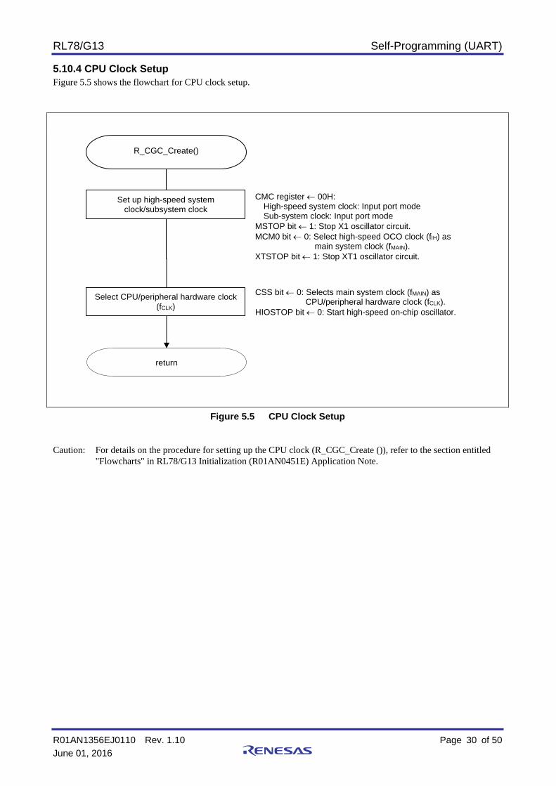
5.10.4 CPU Clock Setup Figure 5.5 shows the flowchart for CPU clock setup.
Figure 5.5 CPU Clock Setup
Caution: For details on the procedure for setting up the CPU clock (R_CGC_Create ()), refer to the section entitled "Flowcharts" in RL78/G13 Initialization (R01AN0451E) Application Note.
R_CGC_Create()
return
Select CPU/peripheral hardware clock (fCLK)
Set up high-speed system clock/subsystem clock
CMC register 00H: High-speed system clock: Input port mode Sub-system clock: Input port mode
MSTOP bit 1: Stop X1 oscillator circuit. MCM0 bit 0: Select high-speed OCO clock (fIH) as
main system clock (fMAIN). XTSTOP bit 1: Stop XT1 oscillator circuit.
CSS bit 0: Selects main system clock (fMAIN) as CPU/peripheral hardware clock (fCLK).
HIOSTOP bit 0: Start high-speed on-chip oscillator.

RL78/G13 Self-Programming (UART)
R01AN1356EJ0110 Rev. 1.10 Page 31 of 50
June 01, 2016
5.10.5 SAU0 Setup Figure 5.6 shows the flowchart for SAU0 setup.
Figure 5.6 SAU0 Setup
R_SAU0_Create()
return
Set up operation of SAU0
Operation clock 0 (CK00): 16 MHz
Supply clock signal to SAU0 SAU0EN bit 1
Set up UART1
R_UART1_Create()
SPS0 register 0011H

RL78/G13 Self-Programming (UART)
R01AN1356EJ0110 Rev. 1.10 Page 32 of 50
June 01, 2016
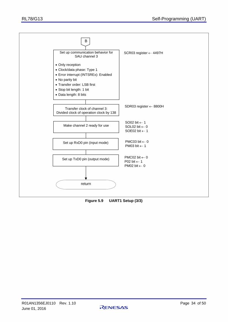
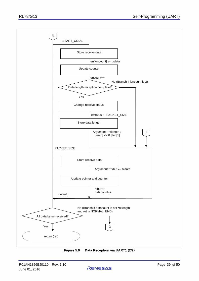
5.10.6 UART1 Setup Figure 5.7 shows the flowchart for UART1 setup (1/3). Figure 5.8 shows the flowchart for UART1 setup (2/3). Figure 5.9 shows the flowchart for UART1 setup (3/3).
Figure 5.7 UART1 Setup (1/3)
R_UART1_Create()
Stop channels 2 and 3 ST0 register 000CH
Disable INTST1 interrupt and clear interrupt request flag
STMK1 bit 1 STIF1 bit 0
Disable INTSR1 interrupt and clear interrupt request flag
SRMK1 bit 1 SRIF1 bit 0
Disable INTSRE1 interrupt and clear interrupt request flag
SREMK1 bit 1 SREIF1 bit 0
Set INTST1 interrupt priority level to 3 (lowest)
STPR11 bit 1 STPR01 bit 1
Set INTSR1 interrupt priority level to 3 (lowest)
SRPR11 bit 1 SRPR01 bit 1
Set INTSRE1 interrupt priority level to 3 (lowest)
SREPR11 bit 1 SREPR01 bit 1
Set up operation mode for SAU channel 2
Operation clock of channel 2:
CK00 Transfer clock of channel 2:
Divided clock of CK00 Detection of falling edge as a start bit
Operation mode of channel 2: UART mode
Interrupt source of channel 2: Transfer end interrupt
SMR02 register 0022H
A

RL78/G13 Self-Programming (UART)
R01AN1356EJ0110 Rev. 1.10 Page 33 of 50
June 01, 2016
Figure 5.8 UART1 Setup (2/3)
A
Set up communication behavior for channel 2 of SAU
Only transmission
Clock/data phase: Type 1
Error interrupt (INTSREx): Masked
No parity bit
Transfer order: LSB first
Stop bit length: 1 bit
Data length: 8 bits
SCR02 register 8097H
Transfer clock of channel 2: Divided clock of operation clock by 138
SDR02 register 8800H
Noise filter of RxD1 pin: On NFEN0 register 04H
SIR03 register 0007H Clear error flag
Set up operation mode for SAU channel 3
Operation clock of channel 3:
CK00 Transfer clock of channel 3:
Divided clock of CK00 Start trigger:
Valid edge of RxD pin Detection of falling edge as a start bit
Operation mode of channel 3: UART mode
Interrupt source of channel 3: Transfer end interrupt
SMR03 register 0122H
B
RL78/G13 Self-Programming (UART)
R01AN1356EJ0110 Rev. 1.10 Page 34 of 50
June 01, 2016
Figure 5.9 UART1 Setup (3/3)
return
B
Set up communication behavior for SAU channel 3
Only reception
Clock/data phase: Type 1
Error interrupt (INTSREx): Enabled
No parity bit
Transfer order: LSB first
Stop bit length: 1 bit
Data length: 8 bits
SCR03 register 4497H
Transfer clock of channel 3: Divided clock of operation clock by 138
SDR03 register 8800H
SO02 bit 1 SOL02 bit 0 SOE02 bit 1
Make channel 2 ready for use
PMC03 bit 0 PM03 bit 1
Set up RxD0 pin (input mode)
PMC02 bit 0 P02 bit 1 PM02 bit 0
Set up TxD0 pin (output mode)
RL78/G13 Self-Programming (UART)
R01AN1356EJ0110 Rev. 1.10 Page 35 of 50
June 01, 2016
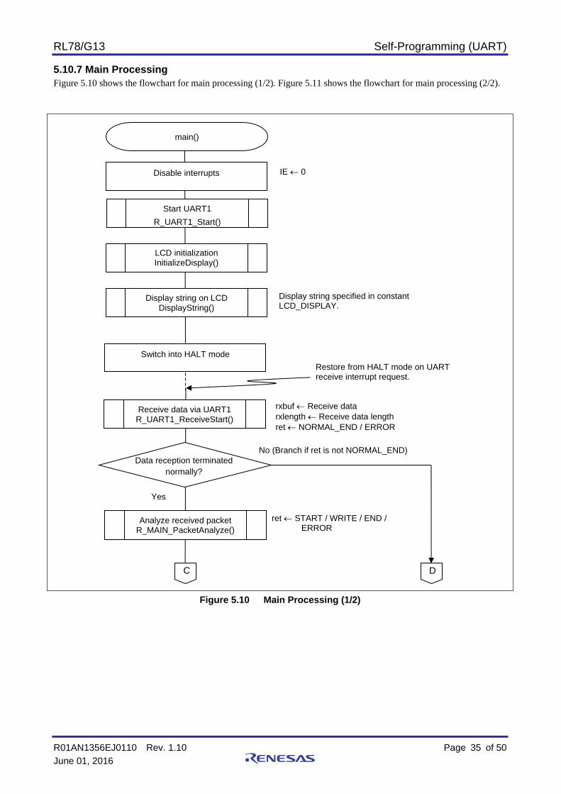
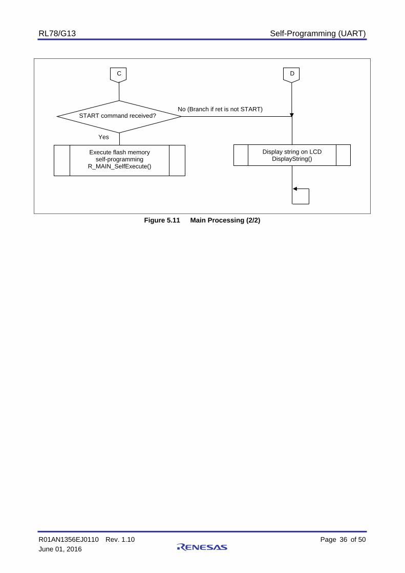
5.10.7 Main Processing Figure 5.10 shows the flowchart for main processing (1/2). Figure 5.11 shows the flowchart for main processing (2/2).
Figure 5.10 Main Processing (1/2)
rxbuf Receive data rxlength Receive data length ret NORMAL_END / ERROR
Data reception terminated normally?
LCD initialization InitializeDisplay()
Display string on LCD DisplayString()
Start UART1
R_UART1_Start()
main()
Disable interrupts
Display string specified in constant LCD_DISPLAY.
IE 0
Switch into HALT mode
Restore from HALT mode on UART receive interrupt request.
No (Branch if ret is not NORMAL_END)
C D
Analyze received packet R_MAIN_PacketAnalyze()
ret START / WRITE / END / ERROR
Receive data via UART1 R_UART1_ReceiveStart()
Yes
RL78/G13 Self-Programming (UART)
R01AN1356EJ0110 Rev. 1.10 Page 36 of 50
June 01, 2016
Figure 5.11 Main Processing (2/2)
C
START command received?
Yes
No (Branch if ret is not START)
Execute flash memory self-programming
R_MAIN_SelfExecute()
Display string on LCD DisplayString()
D
RL78/G13 Self-Programming (UART)
R01AN1356EJ0110 Rev. 1.10 Page 37 of 50
June 01, 2016
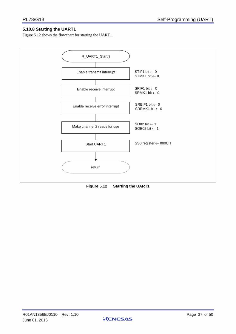
5.10.8 Starting the UART1 Figure 5.12 shows the flowchart for starting the UART1.
Figure 5.12 Starting the UART1
R_UART1_Start()
return
Enable receive interrupt SRIF1 bit 0 SRMK1 bit 0
SO02 bit 1 SOE02 bit 1
Make channel 2 ready for use
SS0 register 000CH Start UART1
Enable receive error interrupt SREIF1 bit 0 SREMK1 bit 0
Enable transmit interrupt STIF1 bit 0 STMK1 bit 0

RL78/G13 Self-Programming (UART)
R01AN1356EJ0110 Rev. 1.10 Page 38 of 50
June 01, 2016
5.10.9 Data Reception via UART1 Figure 5.13 shows the flowchart for data reception via the UART1 (1/2). Figure 5.14 shows the flowchart for data reception via the UART1 (2/2).
Figure 5.13 Data Reception via UART1 (1/2)
R_UART1_ReceiveStart()
Receive data present?
Yes
No (Branch if the BFF01 bit in the SSR03 register is set to 0)
Initialize receive status rxstatus NO_RECEIVE
Set return value to normal termination ret NORMAL_END
Initialize data length receive counter Initialize data receive counter
lencount 0 datacount 0
Initialize receive data length Argument: *rxlength 0xFFFF G
Read receive data
No ((SSR03 & 0x27) is not 0x20)
Branch according to value of rxstatus
Receive status?
NO_RECEIVE
rxdata RXD1 register
No error?
E
Change receive status
Set return value to abnormal termination
F
No (Branch if rxdata is not START_CODE)
Start code received?
ret ERROR
Yes
rxstatus START_CODE
Yes
RL78/G13 Self-Programming (UART)
R01AN1356EJ0110 Rev. 1.10 Page 39 of 50
June 01, 2016
Figure 5.9 Data Reception via UART1 (2/2)
START_CODE
E
Store receive data
Update counter
Data length reception complete?
len[lencount] rxdata
lencount++
Change receive status
rxstatus PACKET_SIZE
Yes
Store data length
Argument: *rxlength len[0] << 8 | len[1]
No (Branch if lencount is 2)
No (Branch if datacount is not *rxlength and ret is NORMAL_END)
rxbuf++ datacount++
Argument: *rxbuf rxdata
G
return (ret)
Store receive data
Update pointer and counter
PACKET_SIZE
F
All data bytes received?
default
Yes

RL78/G13 Self-Programming (UART)
R01AN1356EJ0110 Rev. 1.10 Page 40 of 50
June 01, 2016
5.10.10 Receive Packet Analysis Figure 5.15 shows the flowchart for receive packet analysis.
Figure 5.10 Receive Packet Analysis
R_MAIN_PacketAnalyze()
return (ret)
Initialize loop counter count 0
Initialize checksum checksum 0
Checksum computation complete?No (Branch if argument: (rxlength – 1) ! = count)
Add to checksum
checksum checksum + rxbuf[count]
Update loop count
count++
Checksum match?
Yes
No (Branch if rxbuf[rxlength] != checksum)
Set return value to received command
ret rxdata[0]
Yes
Received command normal?
Yes
Set return value to abnormal termination
ret ERROR
No (Branch if rxbuf[0] is not START, not WRITE, or not END)

RL78/G13 Self-Programming (UART)
R01AN1356EJ0110 Rev. 1.10 Page 41 of 50
June 01, 2016
5.10.11 Flash Memory Self-Programming Execution Figure 5.16 shows the flowchart for flash memory self-programming execution.
Figure 5.16 Flash Memory Self-Programming Execution
R_MAIN_SelfExecute()
WriteAddr 0x1000 Set to start of boot cluster 1. Set up write destination address
P52 bit 0 Turn on LED0
Flash memory self-programming initialization
R_MAIN_SelfInitialize()
ret FSL_OK / FSL_ERR_PARAMETER /
FSL_ERR_ERASE / FSL_ERR_IVERIFY /
FSL_ERR_WRITE / FSL_ERR_FLOW
Initialization terminated normally? No (Branch if ret is not FSL_OK)
Execute flash memory programming
R_MAIN_WriteExecute()
ret FSL_OK / ERROR
Reset FSL_ForceReset()
Internal reset generated
P52 bit 1 Turn off LED0
Programming terminated normally?
No (Branch if ret is not FSL_OK)
Yes
Close flash memory self-programming environment
FSL_Close()
Display “ERROR.”
Display string on LCD DisplayString()
RL78/G13 Self-Programming (UART)
R01AN1356EJ0110 Rev. 1.10 Page 42 of 50
June 01, 2016
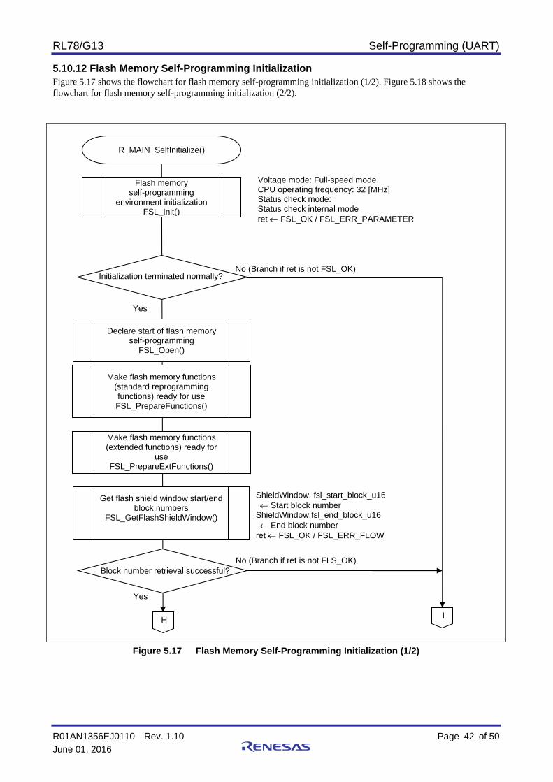
5.10.12 Flash Memory Self-Programming Initialization Figure 5.17 shows the flowchart for flash memory self-programming initialization (1/2). Figure 5.18 shows the flowchart for flash memory self-programming initialization (2/2).
Figure 5.17 Flash Memory Self-Programming Initialization (1/2)
Flash memory self-programming
environment initialization FSL_Init()
H
Initialization terminated normally?
Yes
No (Branch if ret is not FSL_OK)
I
R_MAIN_SelfInitialize()
Block number retrieval successful?
Yes
No (Branch if ret is not FLS_OK)
Voltage mode: Full-speed mode CPU operating frequency: 32 [MHz] Status check mode: Status check internal mode ret FSL_OK / FSL_ERR_PARAMETER
Declare start of flash memory self-programming
FSL_Open()
Make flash memory functions (standard reprogramming functions) ready for use FSL_PrepareFunctions()
Make flash memory functions (extended functions) ready for
use FSL_PrepareExtFunctions()
Get flash shield window start/end block numbers
FSL_GetFlashShieldWindow()
ShieldWindow. fsl_start_block_u16 Start block number ShieldWindow.fsl_end_block_u16 End block number ret FSL_OK / FSL_ERR_FLOW

RL78/G13 Self-Programming (UART)
R01AN1356EJ0110 Rev. 1.10 Page 43 of 50
June 01, 2016
Figure 5.18 Flash Memory Self-Programming Initialization (2/2)
H
All blocks programmable?
Yes
return (ret)
No (Branch if ShieldWindow.fsl_startblock_u16 is not 0 or ShieldWindow.fsl_end_block_u16 is not 63)
I
Flash shield window setup FSL_SetFlashShieldWindow()
Set to: Start block: 0 End block: 63 ret FSL_OK / FSL_ERR_PARAMETER / FSL_ERR_ERASE / FSL_ERR_IVERIFY / FSL_ERR_WRITE / FSL_ERR_FLOW
RL78/G13 Self-Programming (UART)
R01AN1356EJ0110 Rev. 1.10 Page 44 of 50
June 01, 2016
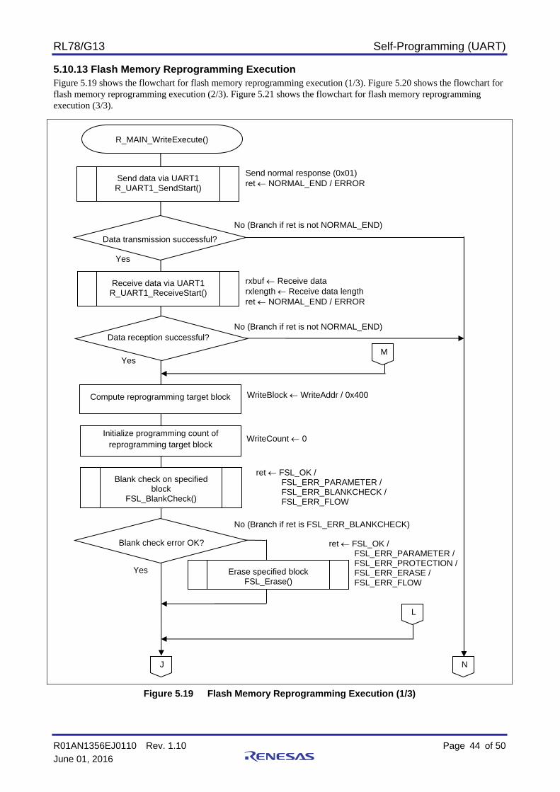
5.10.13 Flash Memory Reprogramming Execution Figure 5.19 shows the flowchart for flash memory reprogramming execution (1/3). Figure 5.20 shows the flowchart for flash memory reprogramming execution (2/3). Figure 5.21 shows the flowchart for flash memory reprogramming execution (3/3).
Figure 5.19 Flash Memory Reprogramming Execution (1/3)
Data reception successful?
Yes
rxbuf Receive data rxlength Receive data length ret NORMAL_END / ERROR
Yes
Receive data via UART1 R_UART1_ReceiveStart()
Initialize programming count of reprogramming target block
Compute reprogramming target block
WriteCount 0
WriteBlock WriteAddr / 0x400
Blank check error OK?
Blank check on specified block
FSL_BlankCheck()
Erase specified block FSL_Erase()
ret FSL_OK / FSL_ERR_PARAMETER /
FSL_ERR_PROTECTION / FSL_ERR_ERASE /
FSL_ERR_FLOW
No (Branch if ret is FSL_ERR_BLANKCHECK)
J N
L
No (Branch if ret is not NORMAL_END)
ret FSL_OK / FSL_ERR_PARAMETER /
FSL_ERR_BLANKCHECK / FSL_ERR_FLOW
M
Send data via UART1 R_UART1_SendStart()
R_MAIN_WriteExecute()
Data transmission successful?
No (Branch if ret is not NORMAL_END)
Send normal response (0x01) ret NORMAL_END / ERROR
Yes

RL78/G13 Self-Programming (UART)
R01AN1356EJ0110 Rev. 1.10 Page 45 of 50
June 01, 2016
Figure 5.20 Flash Memory Reprogramming Execution (2/3)
J
Receive packet analysis R_MAIN_PacketAnalyze()
com START / WRITE / END / ERROR
Write to specified address FSL_Write()
ret FSL_OK / FSL_ERR_PARAMETER /
FSL_ERR_PROTECTION / FSL_ERR_WRITE /
FSL_ERR_FLOW
Write to specified address successful?
Yes
No (Branch if ret is not FLS_OK)
WRITE command received?
Yes
No (Branch if com is not WRITE)
WriteAddr WriteAddr + (rxlength – 2) Update write destination address
K
WriteCount WriteCount + 1 Increment count of reprogramming for block to be reprogrammed
Normal termination?
Yes
No (Branch if ret is not FLS_OK)
O
Send data via UART1 R_UART1_SendStart()
Send normal response (0x01) ret NORMAL_END / ERROR
Data transmission successful?
Yes
No (Branch if ret is not NORMAL_END)
Receive data via UART1 R_UART1_ReceiveStart()
rxbuf Receive data rxlength Receive data length ret NORMAL_END / ERROR
Data reception successful?
Yes
No (Branch if ret is not NORMAL_END)
N

RL78/G13 Self-Programming (UART)
R01AN1356EJ0110 Rev. 1.10 Page 46 of 50
June 01, 2016
Figure 5.21 Flash Memory Reprogramming Execution (3/3)
K O
Anything other than WRITE command received or 1 block reprogramming
complete? L
No (Branch if com is not WRITE or WriteCount is less than 4)
END command received?
Yes
Yes
Verify specified block FSL_IVerify()
ret FSL_OK / FSL_ERR_PARAMETER /
FSL_ERR_PROTECTION / FSL_ERR_FLOW
Verification successful?
Yes
Invert boot flag FSL_InvertBootFlag()
ret FSL_OK / FSL_ERR_PARAMETER /
FSL_ERR_PROTECTION / FSL_ERR_ERASE / FSL_ERR_FLOW FSL_ERR_ERASE
1-block reprogramming complete?
ret FSL_OK / FSL_ERR_PARAMETER /
FSL_ERR_PROTECTION / FSL_ERR_FLOW
Set return value to ERROR
ret ERROR
Verification successful?
Yes
Verify specified block FSL_IVerify()
No (Branch if com is not END)
No (Branch if WriteCount is not 4)
Yes
No (Branch if ret is not FLS_OK)
1
END command received?
Yes
return (ret)
M
No (Branch if com is not END)
No (Branch if ret is not FLS_OK)
1

RL78/G13 Self-Programming (UART)
R01AN1356EJ0110 Rev. 1.10 Page 47 of 50
June 01, 2016
5.10.14 Data Transmission via UART1 Figure 5.22 shows the flowchart for data transmission via the UART1.
Figure 5.22 Data Transmission via UART1
R_UART1_SendStart()
return (ret)
Data not stored in DSDR01 register?
Yes
No (Branch if the BFF01 bit in the SSR02 register is set to 1)
Transmit data TXD1 register Argument: *txbuf
Update pointer and number of transmitted data bytes
txbuf++ Argument: txlength--
All data bytes transmitted?
Yes
No (Branch if txlength is not 0)
Transmitted data bytes greater than or equal to 1?
Yes
No (Branch if argument: txlength is 0 or less)
Set return value to normal termination
ret NORMAL_END
Set return value to abnormal termination
ret ERROR
RL78/G13 Self-Programming (UART)
R01AN1356EJ0110 Rev. 1.10 Page 48 of 50
June 01, 2016
5.11 Operation Check Procedure Change the string defined in the constant LCD_DISPLAY that is defined in r_cg_userdefine.h for the sample program and rebuild the project. Set up to eight characters in the constant LCD_DISPLAY. Flash memory self-programming is carried out by sending the HEX file that is generated as the reprogramming data from the sending side. Refer to Section 5.1, Communication Specifications, for the specifications for the communication between the sending side and this sample program.
For example, the operation of the sample program will look like as shown below when the value of the constant LCD_DISPLAY is changed to "Ver 2.0."
(1) "Ver 1.0" is displayed on the LCD.
The constant LCD_DISPLAY is defined as "Ver 1.0" by this sample program.
(2) Send a START command from the sending side to initiate communication.
After the START command is sent, communication between the sending side and this sample program proceeds as specified in Section 5.1, Communication Specifications.
(3) When the sample program receives a WRITE command and reprogramming data and starts flash memory self-programming, LED0 on the RSK board turns on.
(4) LED0 turns off when the sample program receives an END command.
(5) A reset occurs and "Ver 2.0" is displayed on the LCD.
5.11.1 Making Checks with a Debugger When flash memory self-programming is executed with a debugger (E1 emulator) connected, it becomes unable to check the execution of the program correctly with the debugger after the reprogramming. To check the program execution with the debugger after reprogramming, it is necessary to change the HEX file that is to be used as reprogramming data from the state established immediately when it is generated by CS+.
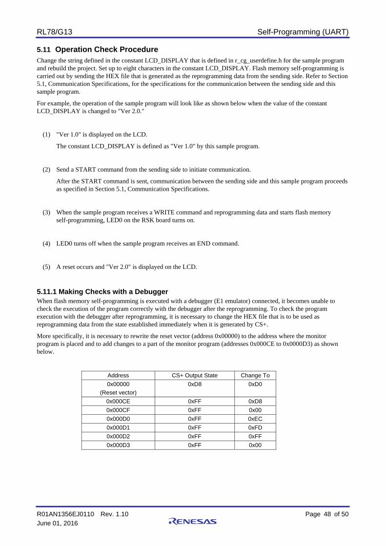
More specifically, it is necessary to rewrite the reset vector (address 0x00000) to the address where the monitor program is placed and to add changes to a part of the monitor program (addresses 0x000CE to 0x0000D3) as shown below.
Address CS+ Output State Change To
0x00000
(Reset vector)
0xD8 0xD0
0x000CE 0xFF 0xD8
0x000CF 0xFF 0x00
0x000D0 0xFF 0xEC
0x000D1 0xFF 0xFD
0x000D2 0xFF 0xFF
0x000D3 0xFF 0x00

RL78/G13 Self-Programming (UART)
R01AN1356EJ0110 Rev. 1.10 Page 49 of 50
June 01, 2016
[Data for normal operation check (CS+ output state)] /* 0000 */ 0xD8, 0x00, 0xFF, 0xFF, 0x56, 0x65, 0x72, 0x20, 0x32, 0x2E, 0x30, 0x20, 0x00, 0x20, 0x45, 0x52,
/* 0010 */ 0x52, 0x4F, 0x52, 0x21, 0x20, 0x00, 0xFE, 0x0F, 0x00, 0xDF, 0x0A, 0xC7, 0x52, 0x12, 0x56, 0x04,
/* 0020 */ 0xFE, 0x11, 0x00, 0xC6, 0xD7, 0x52, 0x1F, 0xD7, 0xC1, 0x51, 0xF3, 0x50, 0x03, 0x5F, 0x90, 0x08,
/* 0030 */ 0x61, 0x48, 0xC0, 0xD7, 0xC7, 0xC5, 0xC1, 0x66, 0x75, 0x30, 0x80, 0x08, 0x16, 0xBF, 0x04, 0x08,
/* 0040 */ 0xFC, 0xF8, 0xFF, 0x0E, 0xD2, 0xDF, 0x10, 0xC3, 0x65, 0x73, 0xF2, 0xA8, 0x02, 0x14, 0x61, 0xE9,
/* 0050 */ 0x99, 0xA5, 0x82, 0x93, 0xDF, 0xF8, 0xC2, 0xC0, 0xC4, 0xC6, 0xD7, 0xFF, 0xFF, 0x00, 0xFF, 0xFF,
/* 0060 */ 0xFF, 0xFF, 0xFF, 0xFF, 0xFF, 0xFF, 0xFF, 0xFF, 0xFF, 0xFF, 0xFF, 0xFF, 0xFF, 0xFF, 0xFF, 0xFF,
/* 0070 */ 0xFF, 0xFF, 0xFF, 0xFF, 0xFF, 0xFF, 0xFF, 0xFF, 0xFF, 0xFF, 0xFF, 0xFF, 0xFF, 0xFF, 0xFF, 0xFF,
/* 0080 */ 0xFF, 0xFF, 0xFF, 0xFF, 0xFF, 0xFF, 0xFF, 0xFF, 0xFF, 0xFF, 0xFF, 0xFF, 0xFF, 0xFF, 0xFF, 0xFF,
/* 0090 */ 0xFF, 0xFF, 0xFF, 0xFF, 0xFF, 0xFF, 0xFF, 0xFF, 0xFF, 0xFF, 0xFF, 0xFF, 0xFF, 0xFF, 0xFF, 0xFF,
/* 00A0 */ 0xFF, 0xFF, 0xFF, 0xFF, 0xFF, 0xFF, 0xFF, 0xFF, 0xFF, 0xFF, 0xFF, 0xFF, 0xFF, 0xFF, 0xFF, 0xFF,
/* 00B0 */ 0xFF, 0xFF, 0xFF, 0xFF, 0xFF, 0xFF, 0xFF, 0xFF, 0xFF, 0xFF, 0xFF, 0xFF, 0xFF, 0xFF, 0xFF, 0xFF,
/* 00C0 */ 0xEF, 0x7F, 0xE8, 0x84, 0x00, 0x00, 0x00, 0x00, 0x00, 0x00, 0x00, 0x00, 0x00, 0x00, 0xFF, 0xFF,
/* 00D0 */ 0xFF, 0xFF, 0xFF, 0xFF, 0xFF, 0xFF, 0xFF, 0xFF, 0x61, 0xCF, 0x51, 0x00, 0x71, 0x8C, 0x71, 0x09,
[Data for debugger operation check] /* 0000 */ 0xD0, 0x00, 0xFF, 0xFF, 0x56, 0x65, 0x72, 0x20, 0x32, 0x2E, 0x30, 0x20, 0x00, 0x20, 0x45, 0x52,
/* 0010 */ 0x52, 0x4F, 0x52, 0x21, 0x20, 0x00, 0xFE, 0x0F, 0x00, 0xDF, 0x0A, 0xC7, 0x52, 0x12, 0x56, 0x04,
/* 0020 */ 0xFE, 0x11, 0x00, 0xC6, 0xD7, 0x52, 0x1F, 0xD7, 0xC1, 0x51, 0xF3, 0x50, 0x03, 0x5F, 0x90, 0x08,
/* 0030 */ 0x61, 0x48, 0xC0, 0xD7, 0xC7, 0xC5, 0xC1, 0x66, 0x75, 0x30, 0x80, 0x08, 0x16, 0xBF, 0x04, 0x08,
/* 0040 */ 0xFC, 0xF8, 0xFF, 0x0E, 0xD2, 0xDF, 0x10, 0xC3, 0x65, 0x73, 0xF2, 0xA8, 0x02, 0x14, 0x61, 0xE9,
/* 0050 */ 0x99, 0xA5, 0x82, 0x93, 0xDF, 0xF8, 0xC2, 0xC0, 0xC4, 0xC6, 0xD7, 0xFF, 0xFF, 0x00, 0xFF, 0xFF,
/* 0060 */ 0xFF, 0xFF, 0xFF, 0xFF, 0xFF, 0xFF, 0xFF, 0xFF, 0xFF, 0xFF, 0xFF, 0xFF, 0xFF, 0xFF, 0xFF, 0xFF,
/* 0070 */ 0xFF, 0xFF, 0xFF, 0xFF, 0xFF, 0xFF, 0xFF, 0xFF, 0xFF, 0xFF, 0xFF, 0xFF, 0xFF, 0xFF, 0xFF, 0xFF,
/* 0080 */ 0xFF, 0xFF, 0xFF, 0xFF, 0xFF, 0xFF, 0xFF, 0xFF, 0xFF, 0xFF, 0xFF, 0xFF, 0xFF, 0xFF, 0xFF, 0xFF,
/* 0090 */ 0xFF, 0xFF, 0xFF, 0xFF, 0xFF, 0xFF, 0xFF, 0xFF, 0xFF, 0xFF, 0xFF, 0xFF, 0xFF, 0xFF, 0xFF, 0xFF,
/* 00A0 */ 0xFF, 0xFF, 0xFF, 0xFF, 0xFF, 0xFF, 0xFF, 0xFF, 0xFF, 0xFF, 0xFF, 0xFF, 0xFF, 0xFF, 0xFF, 0xFF,
/* 00B0 */ 0xFF, 0xFF, 0xFF, 0xFF, 0xFF, 0xFF, 0xFF, 0xFF, 0xFF, 0xFF, 0xFF, 0xFF, 0xFF, 0xFF, 0xFF, 0xFF,
/* 00C0 */ 0xEF, 0x7F, 0xE8, 0x84, 0x00, 0x00, 0x00, 0x00, 0x00, 0x00, 0x00, 0x00, 0x00, 0x00, 0xD8, 0x00,
/* 00D0 */ 0xEC, 0xFD, 0xFF, 0x00, 0xFF, 0xFF, 0xFF, 0xFF, 0x61, 0xCF, 0x51, 0x00, 0x71, 0x8C, 0x71, 0x09,
This sample program generates a reset by inverting the state of the boot flag and carries out boot swapping after rewriting boot cluster 1. The FSL_ForceReset function of the flash memory self-programming library is used to generate the reset. When this function is executed with a debugger (E1 emulator) connected, a break will occur and processing stop. After the break occurs, it is necessary to manually effect a reset and execute the program again.
Change address 00000H from D8H to D0H.
Change addresses 000CEH to 000D3H from FFH, FFH, FFH, FFH, FFH, FFH to D8H, 00H, ECH, FDH, FFH, 00H.

RL78/G13 Self-Programming (UART)
R01AN1356EJ0110 Rev. 1.10 Page 50 of 50
June 01, 2016
6. Sample Code
The sample code is available on the Renesas Electronics Website.
7. Documents for Reference
RL78/G13 User's Manual: Hardware (R01UH0146E)
RL78 Family User's Manual: Software (R01US0015E)
RL78 family’s Flash Self Programming Library Type01 User’s Manual (R01US0050E)
(The latest versions of the documents are available on the Renesas Electronics Website.)
Technical Updates/Technical Brochures
(The latest versions of the documents are available on the Renesas Electronics Website.)
Website and Support
Renesas Electronics Website http://www.renesas.com/index.jsp Inquiries http://www.renesas.com/contact/
A-1
Revision Record RL78/G13 Self-Programming (UART)
Rev. Date Description
Page Summary
1.00 Mar.01, 2013 — First edition issued
1.10 June 01, 2016 11 Modification of 1.4 How to Get the Flash Memory Self-Programming Library.
50 Addition of Documents for Reference.
All trademarks and registered trademarks are the property of their respective owners.

General Precautions in the Handling of MPU/MCU Products The following usage notes are applicable to all MPU/MCU products from Renesas. For detailed usage notes on the products covered by this document, refer to the relevant sections of the document as well as any technical updates that have been issued for the products.
1. Handling of Unused Pins
Handle unused pins in accordance with the directions given under Handling of Unused Pins in the manual.
⎯ The input pins of CMOS products are generally in the high-impedance state. In operation with an unused pin in the open-circuit state, extra electromagnetic noise is induced in the vicinity of LSI, an associated shoot-through current flows internally, and malfunctions occur due to the false recognition of the pin state as an input signal become possible. Unused pins should be handled as described under Handling of Unused Pins in the manual.
2. Processing at Power-on
The state of the product is undefined at the moment when power is supplied.
⎯ The states of internal circuits in the LSI are indeterminate and the states of register settings and pins are undefined at the moment when power is supplied. In a finished product where the reset signal is applied to the external reset pin, the states of pins are not guaranteed from the moment when power is supplied until the reset process is completed. In a similar way, the states of pins in a product that is reset by an on-chip power-on reset function are not guaranteed from the moment when power is supplied until the power reaches the level at which resetting has been specified.
3. Prohibition of Access to Reserved Addresses
Access to reserved addresses is prohibited.
⎯ The reserved addresses are provided for the possible future expansion of functions. Do not access these addresses; the correct operation of LSI is not guaranteed if they are accessed.
4. Clock Signals
After applying a reset, only release the reset line after the operating clock signal has become stable. When switching the clock signal during program execution, wait until the target clock signal has stabilized.
⎯ When the clock signal is generated with an external resonator (or from an external oscillator) during a reset, ensure that the reset line is only released after full stabilization of the clock signal. Moreover, when switching to a clock signal produced with an external resonator (or by an external oscillator) while program execution is in progress, wait until the target clock signal is stable.
5. Differences between Products
Before changing from one product to another, i.e. to a product with a different part number, confirm that the change will not lead to problems.
⎯ The characteristics of an MPU or MCU in the same group but having a different part number may differ in terms of the internal memory capacity, layout pattern, and other factors, which can affect the ranges of electrical characteristics, such as characteristic values, operating margins, immunity to noise, and amount of radiated noise. When changing to a product with a different part number, implement a system-evaluation test for the given product.

Notice1. Descriptions of circuits, software and other related information in this document are provided only to illustrate the operation of semiconductor products and application examples. You are fully responsible for
the incorporation of these circuits, software, and information in the design of your equipment. Renesas Electronics assumes no responsibility for any losses incurred by you or third parties arising from the
use of these circuits, software, or information.
2. Renesas Electronics has used reasonable care in preparing the information included in this document, but Renesas Electronics does not warrant that such information is error free. Renesas Electronics
assumes no liability whatsoever for any damages incurred by you resulting from errors in or omissions from the information included herein.
3. Renesas Electronics does not assume any liability for infringement of patents, copyrights, or other intellectual property rights of third parties by or arising from the use of Renesas Electronics products or
technical information described in this document. No license, express, implied or otherwise, is granted hereby under any patents, copyrights or other intellectual property rights of Renesas Electronics or
others.
4. You should not alter, modify, copy, or otherwise misappropriate any Renesas Electronics product, whether in whole or in part. Renesas Electronics assumes no responsibility for any losses incurred by you or
third parties arising from such alteration, modification, copy or otherwise misappropriation of Renesas Electronics product.
5. Renesas Electronics products are classified according to the following two quality grades: "Standard" and "High Quality". The recommended applications for each Renesas Electronics product depends on
the product's quality grade, as indicated below.
"Standard": Computers; office equipment; communications equipment; test and measurement equipment; audio and visual equipment; home electronic appliances; machine tools; personal electronic
equipment; and industrial robots etc.
"High Quality": Transportation equipment (automobiles, trains, ships, etc.); traffic control systems; anti-disaster systems; anti-crime systems; and safety equipment etc.
Renesas Electronics products are neither intended nor authorized for use in products or systems that may pose a direct threat to human life or bodily injury (artificial life support devices or systems, surgical
implantations etc.), or may cause serious property damages (nuclear reactor control systems, military equipment etc.). You must check the quality grade of each Renesas Electronics product before using it
in a particular application. You may not use any Renesas Electronics product for any application for which it is not intended. Renesas Electronics shall not be in any way liable for any damages or losses
incurred by you or third parties arising from the use of any Renesas Electronics product for which the product is not intended by Renesas Electronics.
6. You should use the Renesas Electronics products described in this document within the range specified by Renesas Electronics, especially with respect to the maximum rating, operating supply voltage
range, movement power voltage range, heat radiation characteristics, installation and other product characteristics. Renesas Electronics shall have no liability for malfunctions or damages arising out of the
use of Renesas Electronics products beyond such specified ranges.
7. Although Renesas Electronics endeavors to improve the quality and reliability of its products, semiconductor products have specific characteristics such as the occurrence of failure at a certain rate and
malfunctions under certain use conditions. Further, Renesas Electronics products are not subject to radiation resistance design. Please be sure to implement safety measures to guard them against the
possibility of physical injury, and injury or damage caused by fire in the event of the failure of a Renesas Electronics product, such as safety design for hardware and software including but not limited to
redundancy, fire control and malfunction prevention, appropriate treatment for aging degradation or any other appropriate measures. Because the evaluation of microcomputer software alone is very difficult,
please evaluate the safety of the final products or systems manufactured by you.
8. Please contact a Renesas Electronics sales office for details as to environmental matters such as the environmental compatibility of each Renesas Electronics product. Please use Renesas Electronics
products in compliance with all applicable laws and regulations that regulate the inclusion or use of controlled substances, including without limitation, the EU RoHS Directive. Renesas Electronics assumes
no liability for damages or losses occurring as a result of your noncompliance with applicable laws and regulations.
9. Renesas Electronics products and technology may not be used for or incorporated into any products or systems whose manufacture, use, or sale is prohibited under any applicable domestic or foreign laws or
regulations. You should not use Renesas Electronics products or technology described in this document for any purpose relating to military applications or use by the military, including but not limited to the
development of weapons of mass destruction. When exporting the Renesas Electronics products or technology described in this document, you should comply with the applicable export control laws and
regulations and follow the procedures required by such laws and regulations.
10. It is the responsibility of the buyer or distributor of Renesas Electronics products, who distributes, disposes of, or otherwise places the product with a third party, to notify such third party in advance of the
contents and conditions set forth in this document, Renesas Electronics assumes no responsibility for any losses incurred by you or third parties as a result of unauthorized use of Renesas Electronics
products.
11. This document may not be reproduced or duplicated in any form, in whole or in part, without prior written consent of Renesas Electronics.
12. Please contact a Renesas Electronics sales office if you have any questions regarding the information contained in this document or Renesas Electronics products, or if you have any other inquiries.
(Note 1) "Renesas Electronics" as used in this document means Renesas Electronics Corporation and also includes its majority-owned subsidiaries.
(Note 2) "Renesas Electronics product(s)" means any product developed or manufactured by or for Renesas Electronics.
http://www.renesas.comRefer to "http://www.renesas.com/" for the latest and detailed information.
Renesas Electronics America Inc.2801 Scott Boulevard Santa Clara, CA 95050-2549, U.S.A.Tel: +1-408-588-6000, Fax: +1-408-588-6130Renesas Electronics Canada Limited9251 Yonge Street, Suite 8309 Richmond Hill, Ontario Canada L4C 9T3Tel: +1-905-237-2004Renesas Electronics Europe LimitedDukes Meadow, Millboard Road, Bourne End, Buckinghamshire, SL8 5FH, U.KTel: +44-1628-585-100, Fax: +44-1628-585-900Renesas Electronics Europe GmbHArcadiastrasse 10, 40472 Düsseldorf, Germany Tel: +49-211-6503-0, Fax: +49-211-6503-1327Renesas Electronics (China) Co., Ltd.Room 1709, Quantum Plaza, No.27 ZhiChunLu Haidian District, Beijing 100191, P.R.ChinaTel: +86-10-8235-1155, Fax: +86-10-8235-7679Renesas Electronics (Shanghai) Co., Ltd.Unit 301, Tower A, Central Towers, 555 Langao Road, Putuo District, Shanghai, P. R. China 200333 Tel: +86-21-2226-0888, Fax: +86-21-2226-0999Renesas Electronics Hong Kong LimitedUnit 1601-1611, 16/F., Tower 2, Grand Century Place, 193 Prince Edward Road West, Mongkok, Kowloon, Hong KongTel: +852-2265-6688, Fax: +852 2886-9022Renesas Electronics Taiwan Co., Ltd.13F, No. 363, Fu Shing North Road, Taipei 10543, TaiwanTel: +886-2-8175-9600, Fax: +886 2-8175-9670Renesas Electronics Singapore Pte. Ltd.80 Bendemeer Road, Unit #06-02 Hyflux Innovation Centre, Singapore 339949Tel: +65-6213-0200, Fax: +65-6213-0300Renesas Electronics Malaysia Sdn.Bhd.Unit 1207, Block B, Menara Amcorp, Amcorp Trade Centre, No. 18, Jln Persiaran Barat, 46050 Petaling Jaya, Selangor Darul Ehsan, MalaysiaTel: +60-3-7955-9390, Fax: +60-3-7955-9510Renesas Electronics India Pvt. Ltd.No.777C, 100 Feet Road, HAL II Stage, Indiranagar, Bangalore, IndiaTel: +91-80-67208700, Fax: +91-80-67208777Renesas Electronics Korea Co., Ltd.12F., 234 Teheran-ro, Gangnam-Gu, Seoul, 135-080, KoreaTel: +82-2-558-3737, Fax: +82-2-558-5141
SALES OFFICES
© 2016 Renesas Electronics Corporation. All rights reserved.Colophon 5.0