rigorous surface enhanced raman spectral characterization of
TRANSCRIPT

Rigorous Surface Enhanced Raman Spectral Characterization of Large-Area High-Uniformity Silver-Coated Tapered Silica NanopillarM. R. Gartia, Z. Xu, E. Behymer, H. Nguyen, J. A. Britten, C. Larson, R. Miles, M. Bora, A. S. Chang, T. C. Bond and G. L. Liu
Nanotechnology
July 23, 2010
LLNL-JRNL-448931

Disclaimer This document was prepared as an account of work sponsored by an agency of the United States government. Neither the United States government nor Lawrence Livermore National Security, LLC, nor any of their employees makes any warranty, expressed or implied, or assumes any legal liability or responsibility for the accuracy, completeness, or usefulness of any information, apparatus, product, or process disclosed, or represents that its use would not infringe privately owned rights. Reference herein to any specific commercial product, process, or service by trade name, trademark, manufacturer, or otherwise does not necessarily constitute or imply its endorsement, recommendation, or favoring by the United States government or Lawrence Livermore National Security, LLC. The views and opinions of authors expressed herein do not necessarily state or reflect those of the United States government or Lawrence Livermore National Security, LLC, and shall not be used for advertising or product endorsement purposes.
Rigorous Surface Enhanced Raman Spectral Characterization of Large-Area High-Uniformity Silver-Coated Tapered Silica Nanopillar Arrays
Manas R. Gartia1, Zhida Xu1, Elaine Behymer2, Hoang Nguyen2, Jerald A. Britten2, Cindy Larson2,Robin Miles2, Mihail Bora2, Allan S.-P. Chang2, Tiziana C. Bond2 and G. Logan Liu1, *
1Micro and Nanotechnology Laboratory, Department of Electrical and Computer Engineering, University of Illinois at Urbana-Champaign; 2Center of Meso, Micro and Nano Scale Technology, Lawrence Livermore National Laboratory
* All correspondences should be sent to Logan Liu [email protected]
Abstract
Surface-Enhanced Raman spectroscopy (SERS) has been increasingly utilized as an analytical technique with significant chemical and biological applications [1-7]. However, production of a robust, homogeneous and large-area SERS substrate with the same ultra high sensitivity and reproducibility still remain an important issue. Here, we describe a large-area ultrahigh-uniformity tapered silver nanopillar array made by laser interference lithography on the entire surface of a 6-inch wafer. Also presented is the rigorous optical characterization method of the tapered nanopillar substrate to accurately quantify the Raman enhancement factor, uniformityand repeatability. An average homogeneous enhancement factor of close to 108 was obtained for benzenethiol adsorbed on a silver coated nanopillar substrate.
Introduction
The extensive use of Raman spectroscopy as a bio-molecule detection tool is still restricted due to its weak sensitivity as compared to other scattering mechanisms (roughly only 1 in 108
photons ends up in Raman scattering) [8] and also due to typical lower scattering cross-sections of Raman process (~ 10-30 cm2) which is around 15 orders of magnitude lower than uorescence emission [9]. In order to get detectable Raman scattering it is necessary to use an array of filtering techniques or to enhance the Raman scattering process. The latter of the two can be achieved using Surface Enhanced Raman Spectroscopy (SERS). In 1997, Kneipp et al. [10] reported that SERS might be capable of single molecule detection. Nie and Emory [11] also independently confirmed the findings and proposed the concept of “hot particles” which are capable of producing very high enhancement (~1014), which can be used for single-molecule detection. The single molecule SERS experiment by Nie and Emory [11] was done with dry silver colloidal particles with Rhodamine 6G molecules, whereas Kneipp et al. [10] did the experiments with crystal violet dye molecule in aqueous colloidal silver solution. The concentrations in both the cases were ultra-low so that there are a small number of analytes per

colloids, typically ~0.1 molecule/colloid. The single-molecule nature of the signals was inferred from the ultra low concentration of the sample. Because of low analyte concentration, it was statistically suggested that there cannot be more than about one molecule per colloid or an average one molecule in the scattering volume if several colloids are present. So, if any SERS signal is observed then it must originate from a single molecule. In the context of single molecule SERS experiment, it should be noted that the experiments were performed with very strong dye molecules (Rhodamine 6G (R6G) and crystal violet), which inherently have Raman cross sections much larger than 10-30 cm2 due to resonance effects (e.g. isolated R6G has a resonance Raman cross section of ~10-24 cm2/sr). Hence, single-molecule detection of R6G can be achieved even with a surface enhancement factor of about 1010. However, above these SERS active substrate preparation processes are hampered by the need to use more time consuming bio-conjugation process of molecule to the colloids. The inherent statistical distribution of colloids in the solution also makes it difficult to get uniform and reproducible detection (and enhancement factor) consistently.
On the other hand, the dramatic development of nanotechnology opens the possibilities of new SERS substrate design and fabrication. One of the many approaches that has been tried includes micro- or nanoscale “roughening,” either in the form of electrochemical texturing of a surface before metal sputtering [12], or as a metal colloid either bonded to a surface [13, 14], or in close proximity to a surface. In the last technique, the sample molecules are placed onto a sol-gel matrix of silver particles coating the inside of a glass vial — the molecules are injected into the vial in solution, permitting SERS of those which then leave the solution and embed themselves into the matrix [15, 16]. The nanoscale approaches also includes (self-) assemblies of latex nanoparticles, which, when electroplated and subsequently dissolved away, leave behind nanovoids or nanoholes (ordered and irregular, respectively) [17, 18]. This popular nanosphere lithography technique has also been applied to create ordered 2D nanoparticle arrays (often called a Fischer pattern), typically using a colloid crystal as evaporation or etching mask [19-21]. In addition, the straightforward binding of molecules to single metal nanoparticles has also been reported to have yielded Raman signal enhancement, leading to the detection of single molecule Raman spectra [10, 11, 22, 23]. In general, reported signal enhancements are as much as sixorders of magnitude or more. However, a mature and sizeable level of commercial success is yet to be achieved by these technologies. In spite of having a fairly reliable manufacturing process in replicating those surfaces, the level of enhancement measured across a single surface remains unacceptably inconsistent. Enhancement is observed only at so-called “hot spots,” regions where the Raman signal is very high, while neighboring regions might exhibit little or even no significant signal enhancement. This situation is exacerbated further by an inconsistency of performance between different but essentially identical substrates [24]. Overall, these twoaspects together effectively have prevented SERS from being widely recognized as a quantifiable spectroscopic technique [25].
In this paper, we describe a rigorous SERS characterization experiment with a substrate made up of silver-coated silica nanopillar arrays produced by large scale laser interference lithography and following metal deposition. The pillars have shown to have great tunability potential [ *]andwith an adiabatic taper of ~25degree offer the additional advantage of nanofocusing and impedance matching [39-40 you just added + . This low cost yet highly-uniform SERS substrate is field deployable, robust and designed for reproducible detection platform for bio-molecules. Here, we describe the optical characterization experiments with the standard Ramanmolecule Benzenethiol (C6H6S), due to its ready nature to form a uniform self assembledmonolayer (SAM) on noble metal material such as silver and gold [26,27] (which are also the preferred material coating for tapered nanopillar SERS substrates because of their optimal plasmon properties in visible range) [28].
SERS substrate preparation
The nanopillar SERS substrates were prepared using the following method. Firstly a 4-inch-diameter silicon dioxide wafer is coated with an average 0.45 μm thick photoresist and then exposed by 413 nm wavelength laser interference illumination with a dose of ~ 40 mJ/cm2. After the photoresist development, the wafer is covered by a uniform array of nanoscale circular photoresist mask of 185 nm in diameter and 370 nm in spacing distance [29]. Secondly the wafer is subject to ion milling deep reactive ion etching by using a highly directional Bosch process. The unprotected silicon diode area was etched down for 500 nm leaving behind the array of silicon dioxide nanopillars. As there is also the lateral etching to the photoresist-protected area, or “undercut”, although at a much slower etch rate, the silicon dioxide nanopillars are tapered and have sharp tips at the top. Finally after completely stripping the photoresist, the wafer covered with nanopillar array structures on the entire surface was subject to metal deposition.
In order to make the nanopillar surfaces SERS active, e-beam evaporation of an 80-nm thick film of silver onto the nanopillar surface was performed. The film was deposited at a rate of 0.1 nm s−1, with no heating or cooling applied to the substrate during deposition. To make the deposition uniform, the sample was kept on a hemispherical mounting rotating with 50 rpm (revolution per minute) inside the e-beam chamber. Figure 1 (a) and (b) show the scanning electron microscope image of the LLNL nanopillar SERS substrate before depositing silver and after coated with 80 nm of silver respectively.

Fig. 1(a) SERS substrate before deposition of silver
(b) Side view (25o) of SERS substrate after depositing 80 nm silver
After the deposition, the silver-coated LLNL substrates were then functionalized with a SAM of benzenethiol using an earlier described procedure [30]. The substrates were submerged in 4-mM solutions of benzenethiol made with ethanol for 1 h and then gently rinsed in neat ethanol for 1 min, followed by drying under a stream of nitrogen.
Experimental Setup
The normal Raman and the SERS spectra of Benzenethiol were measured in a Raman spectrometer system with 785-nm laser excitation. The system comprised a semiconductor 785-nm CW diode laser, a microscopy system and a thermoelectric cooled (−80 ◦C) CCD camera(PIXIS-400, Princeton Instruments). The spectral resolution of the spectrometer was approximately 1.5 cm−1 in the near-infrared range. A 10x microscope objective lens (Mitutoyo infinity-corrected long working distance objectives, Edmund Optics, Part No. NT46-144) with an effective focal length of 20 mm and diameter of 24 mm was used to focus the excitation laser beam onto the sample and to collect the backscattered radiation for input into the Ramanspectrometer. Figure 2 shows the schematic of the SERS experimental set up.

Mirror
Collection lens(N.A. = 0.28)
SERS substrate/ sample
Dichroic
Platform
Spectrometer
CW Laser(785 nm)
Fig. 2: Schematic of SERS experimental set-up
Normal Raman scattering cross-section
Benzenethiol (> 99% purity) was purchased from Sigma-Aldrich. About 0.5 ml of neat benzenethiol was poured into a PDMS cell of thickness 0.5 mm to perform the normal Raman spectra. Figure 3 shows the background corrected RS spectrum of neat benzenethiol obtainedusing 35.0 mW of 785-nm CW laser and 1-s integration time in a 20 µm spot size. Consistent with earlier reported findings [30-36] strong Raman bands are observed at 419 (βCCC+νCS), 621(βCCC+νCS), 704 (βCCC+νCS), 919 (βSH), 1006 (βCCC), 1032 (βCH), 1099 (βCCC+ νCS), 1125 (βCH), 1164 (βCH), 1187(βCH) and 1584 (νCC) cm−1. Here, β and ν indicate the in-plane bending and the stretching modes respectively. Full width at half maximum (FWHM) of the fully resolved 1584 cm−1 band is 25 cm−1. The normal Raman intensity was calculated by integrating the area under the 1584 cm−1 band and was found to be 124 counts.
300 450 600 750 900 1050 1200 1350 1500 1650 1800
0
200
400
600
800
1000
1200
1400
419
701
1006
Ram
an in
tens
ity
Wavenumber (cm-1)
Neat Raman SERS200 counts
1573
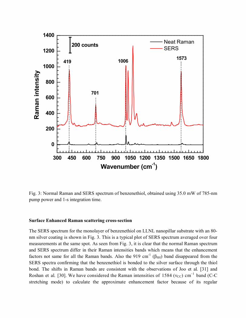
Fig. 3: Normal Raman and SERS spectrum of benzenethiol, obtained using 35.0 mW of 785-nm pump power and 1-s integration time.
Surface Enhanced Raman scattering cross-section
The SERS spectrum for the monolayer of benzenethiol on LLNL nanopillar substrate with an 80-nm silver coating is shown in Fig. 3. This is a typical plot of SERS spectrum averaged over four measurements at the same spot. As seen from Fig. 3, it is clear that the normal Raman spectrum and SERS spectrum differ in their Raman intensities bands which means that the enhancement factors not same for all the Raman bands. Also the 919 cm-1 (βSH) band disappeared from the SERS spectra confirming that the benzenethiol is bonded to the silver surface through the thiol bond. The shifts in Raman bands are consistent with the observations of Joo et al. [31] and Roshan et al. [30]. We have considered the Raman intensities of 1584 (νCC) cm−1 band (C-C stretching mode) to calculate the approximate enhancement factor because of its regular

appearance in both normal Raman and SERS spectrum. It should be noted that there is a slight shift in the Raman band for normal Raman spectrum which occurs at 1584 cm−1 as compared to that of SERS spectrum which occurs at 1573 cm−1. This observation is quite similar to that reported by Roshan et al. [30]. Full width at half maximum (FWHM) of the fully resolved 1573cm−1 band is 12 cm−1. The SERS intensity was calculated by integrating the area under the 1573cm−1 band and was found to be 44593 counts.
Raman scattering length
The Raman scattering length is an important factor in calculating the average enhancement factor of the SERS substrate. For characterizing the Raman scattering length, the neat benzenethiol was carefully mounted in a PDMS cell with a depth of 0.5 mm. The PDMS cell depth was chosen based on the knowledge of depth of focus of the laser system we are using (rule of thumb says the depth of cell should be close or smaller than the depth of focus). The Raman spectrum was taken when the stage was at the equilibrium position (focused position). Subsequently the stage was moved up and down relative to the equilibrium position. Finally, the scattering length was deduced as the length at which the Raman intensity reduced by a factor half of 1/e as compared to the initial equilibrium position intensity. Figure 4 (a) and (b) show a series of Raman spectrum acquired at a regular distance interval of 50 μm covering the total depth of the cell and for the cases when the stage is moving up and down relative to the equilibrium position respectively.

400 800 1200 1600 2000
0
50
100
150
200
250
300
350
400
450
Stage moving down direction
Rel
ativ
e In
tens
ity (c
ount
s)
Wavenumber (cm-1)
500 m
450 m
400 m
350 m
300 m
250 m
200 m
150 m
100 m
50 m
0 m400 800 1200 1600 2000
0
50
100
150
200
250
300
350
400
450
500 m
450 m
400 m
350 m
300 m
250 m
200 m
150 m
100 m
50 mR
elat
ive
Inte
nsity
(cou
nts)
Wavenumber (cm-1)
0 m
Fig. 4: (a) Raman intensity plot when the stageis moving in down direction relative to the equilibrium stage position
(b) Raman intensity plot when the stage is moving in up direction relative to the equilibrium stage position
The variation of Raman intensity as a function of position compared to equilibrium position has also been plotted. Figure 5 shows the variation of Raman intensity of 1584 cm-1 band as a function of position when the stage is moving in down and up direction respectively. As shown in the figure, the intensity keeps on reducing while moving away from the focused position. From the study, it was found that the scattering length for our instrument is 450 μm (distance at which the intensity falls up to 50% of the 1/e value of the maximum).
Depth of focus

-600 -400 -200 0 200 400 6002.5
3.0
3.5
4.0
4.5
5.0
5.5
6.0
6.5 Data Gaussian fit
Inte
nsity
(158
4 cm
-1 p
eak)
Position (m)
0.5*(1/e)*Max.
Max. Intensity
Fig. 5: Variation of Raman intensity for 1584 cm-1 band (obtained using 35.0 mW of 785-nm pump power and 1-s integration time) with distance when the stage is moving in up and down
direction relative to the equilibrium stage position
Area Multiplication Factor
Due to creation of nanopillars, the effective surface area available for formation of monolayer of benzenethiol is increased as compared to flat surface. This factor has to be taken into consideration while calculating the average enhancement factor for the SERS substrate. With a special deposition technique with hemispherical mounting and having the sample at a tilt angle of 25o as well as rotation of 50 rpm, we successfully deposited silver on the side wall of tapered pillars (as shown in the SEM at the inset in Fig. 6(c)). The schematic of nanopillar distribution and shape of the pillar are shown in Fig. 6(a) and (b) respectively. With considering a pillar radius of 75 nm and pillar height of 750 nm, m was calculated to be 2.44 using the relation
21 1 1 1
1 1
[ 9* 9* ]coneA r A AmA

(a)
1μm
1μm
(b)
h
r
s
(c)
Fig. 6: (a) Schematic of average number of pillars per unit area (b) Assumed structure for the nanopillar (c) SEM of LLNL nanopillar substrate with 80 nm silver deposited pillar shown at the inset
Enhancement Factor
The absolute Raman cross-section of Benzenethiol has already been calculated by Roshan et al.[30]. Hence, instead of calculating the absolute Raman cross-section, here focus has been shifted to characterize the effectiveness of current SERS substrate, prepared using a novel laser interference technique, by calculating the enhancement factor (EF). As described in details by Roshan et al. [30], the expression for the enhancement factor can be given as:
Where ISERS and IRS are the Raman intensity from SERS substrate and neat Benzenethiol respectively, NRS is the molecular density of the benzenethiol, NSERS is the areal density of benzenethiol on a flat surface, L is that Raman scattering length, m is multiplier that accounts for the increased surface area of the nanostructured surface and n is the refractive index of benzenethiol. Substituting the values of 1.56 for n [37], 44593 for ISERS, 3.3 x 1014 cm-2 for NSERS, 124 for IRS, and 5.9 x 1021 cm-2 for NRS [30], 0.045 cm (450 μm) for L, 2.44 for m, we obtain a value of average enhancement factor of EFave= 0.4873 x 10⁸ for our tapered nanopillar SERS substrate.
Repeatability of SERS experiment
The repeatability and uniformity of SERS signal across the SERS substrate is an important parameter for designing a robust SERS substrate. The robustness of LLNL nanopillar SERS substrate was characterized by taking several SERS spectrum by scanning the laser across the substrate. The SERS substrate was mounted on a motorized platform which was controlled by LABVIEW program. The sample was scanned for total of 57 data points and at each point, the measurement was repeated 4 times (total sample space of 228 points). A typical 5x5 arrays 2-D
1 μm
2
1* *SERS RS
RS SERS
I N LEFI N m n

scanning result is reported in Fig. 7 (a). The scanning scheme is given at the inset. The SERS peak intensity distribution for a typical peak (1573 cm-1) obtained using 35.0 mW of 785-nm pump power and 1-s integration time is reported in Fig. 7 (b). The surface plot showing the 2-D scanning result has been shown in Fig. 7 (c). To confirm the robustness of the substrate the intensity distribution of SERS spectra was also calculated for many other peaks (1573, 1099, 1006, 704 and 419 cm-1) and shown in Fig. 7 (d). The distributions for all the peaks are found to be following a gaussian distribution. However, 1573 cm-1 peak, which was used for calculating SERS enhancement factor, was found to be fairly uniform. Finally Fig. 8 shows the probabilitydistribution of the enhancement factor calculated for the entire substrate. This follows a Gaussian distribution with a maximum enhancement factor of 0.886 x 10⁸ and an average enhancement factor of 0.25 x 10⁸. This showed the uniformity of the SERS substrate and confirmed that LLNL nanopillar SERS substrate is fairly robust.
Ram
an in
tens
ity
0 5 10 15 20 250
200
400
600
800
1000
1200
1400In
tens
ity o
f 157
3 cm
-1 p
eak
Scan point number
Mean = 890Standard deviation = 137
Fig. 7: (a) 2-D scanning SERS data for the LLNL nanopillar substrate obtained using 35.0 mW of 785-nm pump power and 1-s integration time.
( b ) 2-D scanning SERS intensity distribution for 1573 cm-1 Raman peak-distribution (mean of 890 + 137)
1 2 3 4 5
25
50 μm
50 μm

300 600 900 1200 1500 1800
5
10
15
20
25
Array i
ndex
0
Wave number (cm-1)
500 counts
Fig. 7: (c) Surface plot of 2-D scanning SERS data for the LLNL nanopillar substrate obtained using 35.0 mW of 785-nm pump power and 1-s integration time.

0 10 20 30
600
800
1000
1200600
800
1000
1200
1400
1600600
800
1000
1200
1400200
400
600
800400
600
800
1000
1200
Peak
157
3
Array Number
Peak
109
9Pe
ak 1
006
Peak
704
Peak
419
0 1 2 3 4 5 6 7 8 9 10Occurrence (Counts)
Ram
an In
tens
ity
Fig. 7 (d): SERS intensity distribution for various Raman peak (1573, 1099, 1006, 704 and 419cm-1) and the histogram showing the number of occurrence of particular intensity value

0 1x10⁷ 2x10⁷ 3x10⁷ 4x10⁷ 5x10⁷ 6x10⁷ 7x10⁷ 8x10⁷ 9x1070
5
10
15
20
25C
ount
Enhancement Factor
Probability distribution (Gaussian)
Fig. 8: Probability distribution showing the enhancement factor calculated for the entire substrate
Discussion on Nanopillar Array SERS Substrate
In general, two mechanisms are responsible for the SERS enhancement: the electromagnetic (EM) effect and the chemical or charge transfer (CT) effect. The EM mechanism in particular is related to the morphology of the substrate and hence relevant to the current discussion.
In EM mechanism, surface plasmons on the surface of the metal (nano structure) are excited by incident laser light. It should be noted that the electromagnetic fields can be strongly enhanced in the presence of surface plasmons only if certain resonance conditions are fulfilled. Finally, the product of the enhancement of the incident laser field and the scattered Raman yields the observed overall electromagnetic SERS effect. It is also well known from the TERS (Tip Enhanced Raman Spectroscopy) experience that sharp metal tip can highly confine the electromagnetic field at the apex of a tip (due to an electrostatic lightning rod effect as a result of the shape of the tip) [38]. The high electromagnetic field at the tip is also due to the surface plasmon resonances which correlate the wavelength of the excitation source and the actual tipgeometry. In addition it was also predicted theoretically that optical energy can be nano-focused in a tapered plasmonic waveguides [39]. The enhanced electromagnetic field relies on the

concentration of optical energy in a localized spot (so called “hot spot”). In a nanopillar arrays this can be done by exciting the surface plasmon polaritons (SPP’s) propagating toward a tip of a tapered dielectric coated metal array [40]. This propagation of SPP’s undergoes a rapid adiabaticslowing down and asymptotic stopping at the tip due to boundary condition. This phenomenon leads to a giant concentration of energy on the nanoscale. In a sense the SPP’s are adiabatically transformed into localized surface plasmons (SP’s) [39].
It is believed that the gap between nanopillar can contribute additional localized surface Plasmon resonance, thereby enhancing the electromagnetic field [41, 42]. It is also well known that coupling of propagating surface plasmon polariton (PSSP) to light is possible by creating a grating like structure on surface (nanopillar arrays). This is because of relaxation of conservation of momentum restriction or so called “breaking the translational invariance” [43].
Preliminary optical characterization on a Zeiss reflection microscope for the nanopillar substrate showed a reflectance dip near 700 nm (Fig. 1). Similarly strong absorption peak near 700 nm can be seen in the extinction spectra (Fig. 2). Due to strong dependence of SERS enhancement on the overlap between the incident light and the plasmon resonance, we have used 785 nm laser light for the excitation of surface Plasmon in our experiment.
400 500 600 700 800 9000.08
0.10
0.12
0.14
0.16
0.18
0.20
Ref
lect
ance
(a.u
.)
Wavelength (nm)400 500 600 700 800 900
0.70
0.72
0.74
0.76
0.78
0.80
0.82
0.84
0.86
0.88
0.90
Extin
ctio
n (a
.u.)
Wavelength (nm)
Fig. 9: Reflectance spectra of nanopillar SERS substrate
Fig. 10: Extinction spectra of nanopillar SERS substrate
Conclusion
In conclusion, we have produced a highly ordered Ag coated nanopillar SERS substrate using a novel laser interference nano-lithography technique. A uniform enhancement of ~ 7x 10⁸ (with

peaks at 0.25x10^8) has been demonstrated using a SAM of benzenethiol on the SERS substrate. From the results, it can be inferred that the laser interference based approach is capable of fabricating large area uniform SERS active substrates. This simple and straightforward method for fabricating SERS substrates offers considerable potential for the batch fabrication as well as commercialization of such robust substrate, and hence opens the door for practical sensor chips based on SERS.
Acknowledgement
This work performed under the auspices of DOE by LLNL under Contract DE-AC52-07NA27344. We also acknowledge support by the Defense Advanced Research Projects Agency (DARPA).
References
[1] X. Qian, X.H. Peng, D.O. Ansari, Q.Y. Goen, G.Z. Chen, D.M. Shin, L. Yang, A.N. Young, M.D. Wang and S. Nie, In vivo tumor targeting and spectroscopic detection with surface-enhanced Raman nanoparticle tags, Nature Biotechnology, 26: 83 (2008).
[2] K. Fujita, S. Ishitobi, K. Hamada and N.I. Smith, Time-resolved observation of surface-enhanced Raman scattering from gold nanoparticles during transport through a living cell, J. Biomed. Opt., 14: 024038 (2009).
[3] I.H. Chou, M. Benford, H.T. Beier, G.L. Coté, M. Wang, N. Jing, J. Kameoka, T.A. Good, Nanofluidic biosensing for beta-amyloid detection using surface enhanced Raman spectroscopy, Nano Lett., 8(6):1729 (2008).
[4] M. Culha, D. Stokes, L.R. Allain, and T. Vo-Dinh, Surface-Enhanced Raman Scattering Substrate Based on a Self-Assembled Monolayer for Use in Gene Diagnostics, Anal. Chem., 75: 6196 (2003).
[5] K.A. Willets, Surface-enhanced Raman scattering (SERS) for probing internal cellular structure and dynamics, Anal Bioanal Chem, 394: 85 (2009).
[6] X.X. Han, B. Zhao and Y. Ozaki, Surface-enhanced Raman scattering for protein detection, Anal Bioanal Chem, 394: 1719 (2009).
[7] M.Y. Sha, H. Xu, M. J. Natan and R. Cromer, Surface-Enhanced Raman Scattering Tags for Rapid and Homogeneous Detection of Circulating Tumor Cells in the Presence of Human Whole Blood, J. Am. Chem. Soc., 130(51): 17214 (2008).

[8] R.M. Jarvis and R. Goodacre, Discrimination of Bacteria Using Surface-Enhanced Raman Spectroscopy, Anal. Chem., 76: 40 (2004).
[9] T. Vo-Dinh, L. R. Allain and D. L. Stokes, Cancer gene detection using surface-enhanced Raman scattering (SERS), J. Raman Spectrosc. 33: 511 (2002).
[10] K. Kneipp, Y. Wang, H. Kneipp, L. T. Perelman, I. Itzkan, R. R. Dasari, and M. S. Feld, Single Molecule Detection Using Surface-Enhanced Raman Scattering (SERS), Phys. Rev. Lett., 78: 1667 (1997).
[11] S. Nie and S. R. Emory, Probing Single Molecules and Single Nanoparticles by Surface-Enhanced Raman Scattering, Science, 275: 1102 (1997).
[12] C.A. Murray, D.L. Allara, and M. Rhinewine, Silver molecule separation dependence of surface enhanced Raman scattering, Phys. Rev. Lett., 46: 57 (1981).
[13] L.A. Dick, A.D. Mcfarland, C.L. Haynes, and R.P. Van Duyne, Metal Film over Nanosphere (MFON) Electrodes for Surface-Enhanced Raman Spectroscopy (SERS): Improvements in Surface Nanostructure Stability and Suppression of Irreversible Loss, J. Phys. Chem. B, 106: 853–860 (2002).
[14] T. Vo-Dinh, SERS chemical sensors and biosensors: new tools for environmental and biological analysis, Sensors and Actuators B 29, 183–189, (1995).
[15] http://www.rta.biz/Content/SERV_Vials.asp.
[16] S. Farquharson , F. E. Inscore and S. Christesen, Detecting Chemical Agents and Their Hydrolysis Products in Water, Surface-Enhanced Raman Scattering, 447-460, Springer, 103 (2006).
[17] M.C. Netti, S. Coyle, J.J. Baumberg, M.A. Ghanem, P.R. Birkin, P.N. Bartlett, D.M. Whittaker, Confined Surface Plasmons in Gold Photonic Nanocavities, Adv. Mat. 13 1368–1370 (2001).
[18] S. Coyle, M.C. Netti, J.J. Baumberg, M.A. Ghanem, P.R. Birkin, P.N. Bartlett, and D.M. Whittaker, Confined Plasmons in Metallic Nanocavities, Phys. Rev. Lett. 87, 176801 (2001).
[19] U. C. Fischer and H. P. Zingsheim, Submicroscopic pattern replication with visible light, J. Vac. Sci. Technol., 19: 881-885 (1981).
[20] U. C. Fischer, J. Heimel, H.J. Maas, M. Hartig, S. Hoeppener and H. Fuchs, Latex bead projection Nanopatterns, Surf. Interface Anal., 33: 75–80 (2002).

[21] C. L. Haynes and R. P. Van Duyne, Nanosphere Lithography: A Versatile Nanofabrication Tool for Studies of Size-Dependent Nanoparticle Optics, J. Phys. Chem. B, 105: 5599-5611(2001).
[22] S.R. Emory and S. Nie, Near-Field Surface-Enhanced Raman Spectroscopy on Single Silver Nanoparticles, Anal. Chem. 69: 2631 (1997).
[23] K. Kneipp, Y. Wang, H. Kneipp, I. Itzkan, R.R. Dasari, and M.S. Feld, Population Pumping of Excited Vibrational States by Spontaneous Surface-Enhanced Raman Scattering Phys. Rev. Lett., 76: 2444 (1996).
[24] C. Netti, J. Lincoln, and G. Flinn, Reliable Substrate Technology for Surface Enhanced Raman Spectroscopy, Raman Technology For Today’s Spectroscopists, June 2005.
[25] P. G. Etchegoin and E. C. Le Ru, A perspective on single molecule SERS: current status and future challenges, Phys. Chem. Chem. Phys., 10: 6079 – 6089 (2008).
[26] J. Y. Gui, A. Stern, D. G. Frank, F. Lu, D. C. Zapien, A. T.Hubbard, Adsorption and surface Structural Chemistry of Thiophenol, Benzyl Mercaptan, and Alkyl Mercaptans. Comparative studies at Ag(111) and Pt(111) Electrodes by Means of Auger Spectroscopy, Electron Energy Loss Spectroscopy, Low-Energy Electron Diffraction, and Electroc hemistry, Langmuir 1991, 7, 955 (1991).
[27] H. Kang, T. Park, I. Choi, Y. Lee, E. Ito, M. Hara and J. Noh, Formation of large ordered domains in benzenethiol self-assembled monolayers on Au(1 1 1) observed by scanning tunneling microscopy, Ultramicroscopy,109: 1011-1014 (2009).
[28] M. Bora, B. Fasenfest, J. Chan, E. Behymer, T.C. Bond, Plasmon resonant cavities in vertical nanowire arrays, submitted to Nano Letters (2010).
[29] A. Fernandez, H.T. Nguyen, J.A. Britten, R.D. Boyd, M.D. Perry, D.R. Kania and A.M. Hawryluk, Use of interference lithography to pattern arrays of submicron resist structures for field emission flat panel displays, Journal of Vacuum Science & Technology B, 15, 729 (1997).
[30] R. L. Aggarwal, L. W. Farrar, E. D. Diebold and D. L. Polla, Measurement of the absolute Raman scattering cross section of the 1584-cm−1 band of benzenethiol and the surface-enhanced Raman scattering cross section enhancement factor for femtosecond laser-nanostructured substrates, J. Raman Spectrosc., 40: 1331 (2009).
[31] T. H. Joo, M. Soo, K. Kim, Surface-enhanced Raman scattering of benzenethiol in silver sol, J. Raman Spectrosc., 18: 57 (1987).
[32] D. Lin-Vien,N. B. Colthup,W. G. Fateley, J. G. Grasselli, The Handbook of Infrared and Raman Characteristic Frequencies of Organic Molecules, Academic Press: New York, 1991.
[33] G. Varsanyi, Vibrational Spectra of Benzene Derivatives, Academic Press: New York, 1969.
[34] L.J. Wan, M. Terashima, H. Noda and M. Osawa, Molecular Orientation and Ordered Structure of Benzenethiol Adsorbed on Gold (111), J. Phys. Chem. B, 104, 3563-3569 (2000).
[35] K. T. Camon and L. G. Hurley, Axial and Azimuthal Angle Determination with Surface-Enhanced Raman Spectroscopy: Thiophenol on Copper, Silver, and Gold Metal Surfaces, J. Phys. Chem., 95: 9979-9984 (1991).
[36] S. J. Lee and K. Kim, Development of silver film via thermal decomposition of layered silver alkanecarboxylates for surface-enhanced Raman spectroscopy, Chemical Communication, 212 (2003).
[37] S. Mathias, E. Carvalho Filho, E. G. Cecchini, The dipole moments of cyclohexanethiol, a-toluenethiol and benzenethiol, J. Phys. Chem., 65: 425 (1961).
[38] Bailoa and Deckert, Chem. Soc. Rev., 2008, 37, 921–930
[39] M.I. Stockman, Physical Review Letters, 93, 137404-1, 2004
[40] D.K. Gramotnev et al., Journal of Applied Physics, 104, 034311, 2008
[41] P.J. Recee, Nature photonics, 2, 333, 2008
[42] A. N. Grigorenko et al., Nature photonics, 2, 365, 2008
[43] E.C. Le Ru and P.G. Etchegoin, Page-162, Principles of Surface Enhanced Raman Spectroscopy, Elsevier, 2009