rhepp-1 ion exposure and z x-ray exposure updatearies.ucsd.edu/hapl/meetings/0503-hapl/renk.pdf ·...
TRANSCRIPT

RHEPP-1 Ion Exposure and Z X-Ray Exposure Update
Tim RenkSandia National Laboratories
Beam Applications & Initiatives Department
HAPL Program WorkshopWashington, DCMarch 3-4, 2005
Supported by NRL by the HAPL program by DOE NNSA DP
Sandia is a multiprogram laboratory operated by Sandia Corporation, a Lockheed Martin Company,for the United States Department of Energy under contract DE-AC04-94AL85000.

Pulsed Power Sciences, Sandia National LaboratoriesTJR 6/11/2004
Presentation Outline
• RHEPP - Z series: background briefing
• Z data: latest roughening threshold behavior for W
• Whither Baklava
• New RHEPP Super KS 2000 Series

Regimes of IFE Materials Response Studies for x-rays and ions
AblationDepth (µm) Net AblationNo net ablation, but
surface roughening
F(J/cm2)Threshold for ablation
Threshold for roughening
Goals (for each material): examine net ablation to validate codesfind threshold for ablationunderstand rougheningfind threshold for roughening
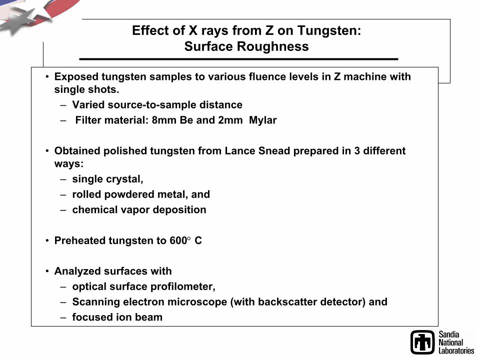
Effect of X rays from Z on Tungsten: Surface Roughness
• Exposed tungsten samples to various fluence levels in Z machine with single shots.
– Varied source-to-sample distance– Filter material: 8mm Be and 2mm Mylar
• Obtained polished tungsten from Lance Snead prepared in 3 different ways:
– single crystal, – rolled powdered metal, and – chemical vapor deposition
• Preheated tungsten to 600° C
• Analyzed surfaces with– optical surface profilometer, – Scanning electron microscope (with backscatter detector) and – focused ion beam
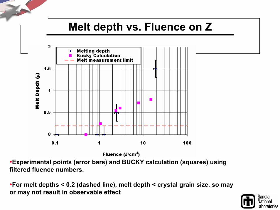
Melt depth vs. Fluence on Z
•Experimental points (error bars) and BUCKY calculation (squares) using filtered fluence numbers.
•For melt depths < 0.2 (dashed line), melt depth < crystal grain size, so may or may not result in observable effect

Images from samples on Z from VEECO surface profiler
Fluence(J/cm2)
Single X Rolled Powder Chemical Vapor Dep
0
0.27
0.9

Roughening Depends on Fluenceand Grain Boundaries
0
50
100
150
200
250
0 0.2 0.4 0.6 0.8 1
Fluence (J/cm2)
Rou
ghne
ss R
a (nm
)
Single crystalPWMCVD
Poly-crystalline
Single crystal
The roughening threshold is ~0.9 J/cm2 for single crystal and is ∼<0.3 J/cm2
for polycrystalline tungsten

The MAP (Magnetically Confined Anode Plasma) Ion Sourceis used for surface modification experiments on RHEPP-1
Pulsed Power Sciences, Sandia National LaboratoriesTJR 7/08/2004
• 600-800 kV• < 250 A/cm2
• Beams from H, He, N2, O2, Ne, Ar, Xe, Kr, CH4
• Overall treatment area ~ 100 cm2
• Diode vacuum ~ 10-5 Torr
Cathode
AnodeFast Coil
Beam
CL
GasPlenum
Target Tablewith Faraday cupArray
�
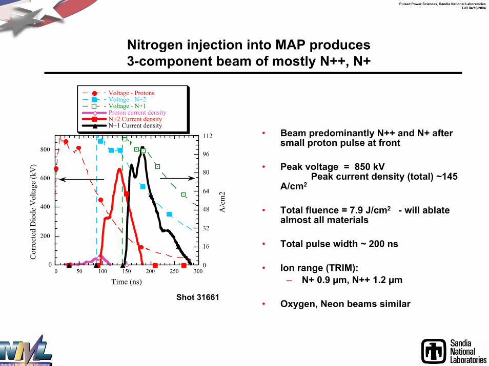
Nitrogen injection into MAP produces 3-component beam of mostly N++, N+
• Beam predominantly N++ and N+ after small proton pulse at front
• Peak voltage = 850 kV Peak current density (total) ~145
A/cm2
• Total fluence = 7.9 J/cm2 - will ablate almost all materials
• Total pulse width ~ 200 ns
• Ion range (TRIM): – N+ 0.9 µm, N++ 1.2 µm
• Oxygen, Neon beams similar
0
200
400
600
800
0 50 100 150 200 250 300
Voltage - ProtonsVoltage - N+2Voltage - N+1Proton current densityN+2 Current densityN+1 Current density
0
16
32
48
64
80
96
112
Time (ns)
Cor
rect
ed D
iode
Vol
tage
(kV
)
A/c
m2
Shot 31661
Pulsed Power Sciences, Sandia National LaboratoriesTJR 04/16/2004

Thresholds for Materials exposure to ions on RHEPP
• General exposure conditions: MAP nitrogen beam, 150 ns pulsewidth, single shot.
• Roughening threshold for graphite (matrix) is unknown, but probably below 0.5 J/cm2
• Roughening threshold for W for He beam is below that for MAP N
• Roughening threshold (Single Pulse), unheated, for
W25Re: 3.5 J/cm2
Re: 1 J/cm2
Roughening threshold, PM W (Schwarzkopf), unheated
Ablation threshold, W
Melting threshold, W, 600C, SIM and expt2.0 J/cm2
3 J/cm2 Ablation threshold, graphites,BUCKY and expt
Pulsed Power Sciences, Sandia National LaboratoriesTJR 04/16/2004
6 J/cm2
1.25 J/cm2
? Roughening threshold, Graphite
0
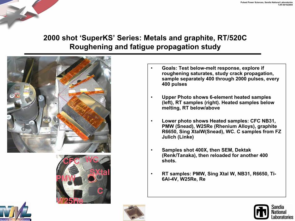
2000 shot ‘SuperKS’ Series: Metals and graphite, RT/520CRoughening and fatigue propagation study
Pulsed Power Sciences, Sandia National LaboratoriesTJR 04/16/2004
• Goals: Test below-melt response, explore if roughening saturates, study crack propagation, sample separately 400 through 2000 pulses, every 400 pulses
• Upper Photo shows 6-element heated samples (left), RT samples (right). Heated samples below melting, RT below/above
• Lower photo shows Heated samples: CFC NB31, PMW (Snead), W25Re (Rhenium Alloys), graphite R6650, Sing XtalW(Snead), WC. C samples from FZ Julich (Linke)
• Samples shot 400X, then SEM, Dektak(Renk/Tanaka), then reloaded for another 400 shots.
• RT samples: PMW, Sing Xtal W, NB31, R6650, Ti-6Al-4V, W25Re, Re
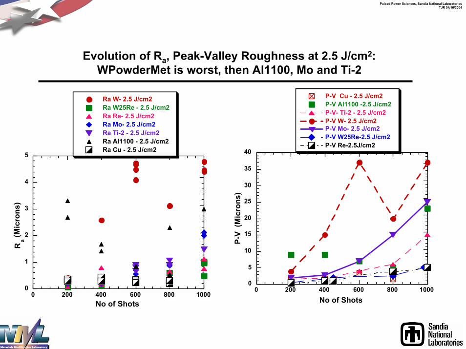
Evolution of Ra, Peak-Valley Roughness at 2.5 J/cm2:WPowderMet is worst, then Al1100, Mo and Ti-2
0
1
2
3
4
5
0 200 400 600 800 1000
Ra W- 2.5 J/cm2Ra W25Re - 2.5 J/cm2Ra Re- 2.5 J/cm2Ra Mo- 2.5 J/cm2Ra Ti-2 - 2.5 J/cm2Ra Al1100 - 2.5 J/cm2Ra Cu - 2.5 J/cm2
Ra (M
icro
ns)
No of Shots
0
5
10
15
20
25
30
35
40
0 200 400 600 800 1000
P-V Cu - 2.5 J/cm2P-V Al1100 -2.5 J/cm2P-V- Ti-2 - 2.5 J/cm2P-V W- 2.5 J/cm2P-V Mo- 2.5 J/cm2P-V W25Re-2.5 J/cm2P-V Re-2.5J/cm2
P-V
(Mic
rons
)
No of Shots
Pulsed Power Sciences, Sandia National LaboratoriesTJR 04/16/2004
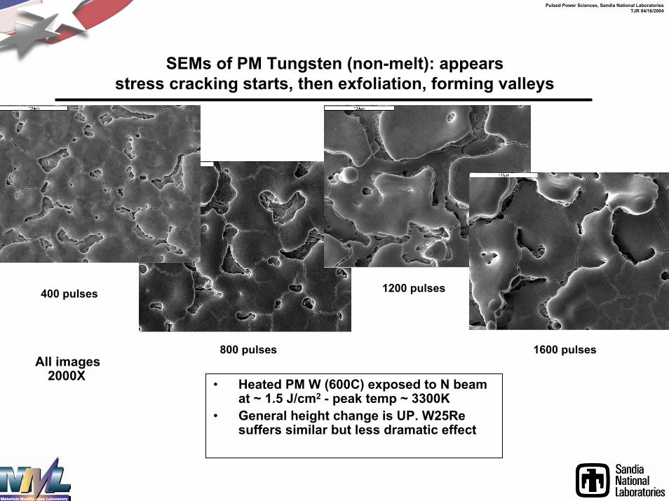
SEMs of PM Tungsten (non-melt): appears stress cracking starts, then exfoliation, forming valleys
Pulsed Power Sciences, Sandia National LaboratoriesTJR 04/16/2004
400 pulses 1200 pulses
800 pulses 1600 pulsesAll images
2000X • Heated PM W (600C) exposed to N beam at ~ 1.5 J/cm2 - peak temp ~ 3300K
• General height change is UP. W25Re suffers similar but less dramatic effect

W25Re: cracking/valley formation process more muted. But is this enough of a solution?
Pulsed Power Sciences, Sandia National LaboratoriesTJR 04/16/2004
• Depth of cracks in right image unknown.
400 pulses 800 pulses 1200 pulsesAll images 2000X
New W25Re @ 400 pulses

Pulsed Power Sciences, Sandia National LaboratoriesTJR 04/16/2004
PM Tungsten after 1600 pulses (non-melting):Mostly mountains
• Heated/treated PM W examined with NEXIV laser interferometry
• Comprehensive line-out scan: max height 30 µm, min height < 10 µm compared to untreated
• There is additional very deep microcracking not visible here

‘Baklava’: Horizontal laminar separation of treated PM Wthat extends far beyond heat-affected zone ( ~ 10 µm)
Pulsed Power Sciences, Sandia National Laboratories
TJR 11/25/03
Photomicrograph, side view, PM W (Schwarzkopf), 1600 pulses, surface temp to near-melt. Vertical height ~ 1.2 mm
Side-image, PM W Schwarzkopf, 125 pulses above melt. Clip holds untreated area

Comparison, treated PMW and W25Re, side view (Uncut), 1600 pulses: ‘Laminated’ structure to 1mm depth on W, missing in W25Re
Pulsed Power Sciences, Sandia National Laboratories
TJR 11/25/03
Photomicrographs, side view, 1600 pulses, surface temp to near-melt
Surface to near-middle (~ 0.8 mm)
Surface to near-middle (~ 0.6 mm)
0.8 mm to ~ 1.5 mm
0.6 mm to ~ 1.2 mm
(Left): Dark horizontal lines represent possible delamareas W25RePM Tungsten:
‘Baklava’ effect’

FIB-XTEM of 1000-pulse W at 2.25 J/cm2 (ave):Deep horizontal/vertical cracking without melt
Pulsed Power Sciences, Sandia National Laboratories
TJR 11/25/03
5 - 10 µm depth
Note: this FIB SampleFell apart
Near-surface
• Polished Powder Met W exposed to 100 shots N beam @ 2.25 J/cm2 ave /pulse, ~ melting temperature at surface. No melt layer observed.
• 600°C exposure• Sample cracking horizontally/vertically down to 10 µm depth• Suspect fatigue-cracking
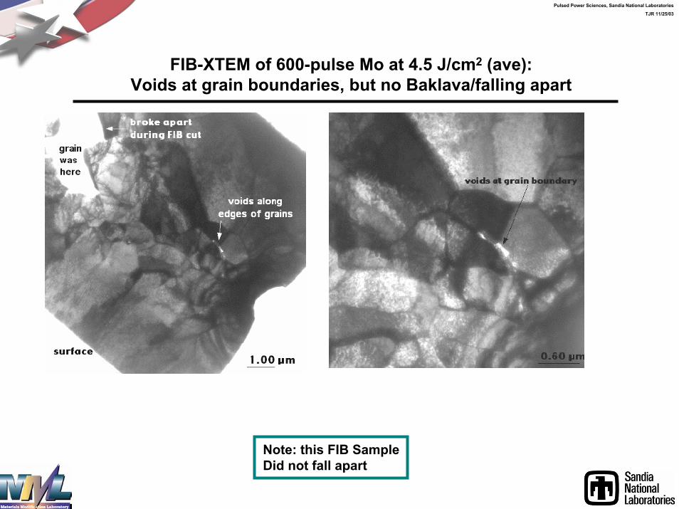
FIB-XTEM of 600-pulse Mo at 4.5 J/cm2 (ave):Voids at grain boundaries, but no Baklava/falling apart
Pulsed Power Sciences, Sandia National Laboratories
TJR 11/25/03
Note: this FIB SampleDid not fall apart

XTEM of 60X-treated PM W (right) show no cracking in depth
Pulsed Power Sciences, Sandia National LaboratoriesTJR 11/25/03
Bright-Field TEM image TEM image from 5 µm depth
Note: This PM W at 60 pulses does NOT exhibit Baklava

‘Baklava’ - Summary
Pulsed Power Sciences, Sandia National Laboratories
TJR 11/25/03
• Laminar separation occurs on PMW Schwarzkopf, either FIB or saw-cut. Material is hot-rolled 50% deformed, similar to Snead W (Alfa Aesar)
• Length scale (500-1200 µ) way beyond ion range
• Lesser fluence/lesser pulse number produces less thickness
• Untreated W - striated structure, but does not delam
• W25Re does not striate or delam
Side-image, PM W Schwarzkopf, 125 pulses above melt. Clip holds untreated area
Pulsed Power Sciences, Sandia National LaboratoriesTJR 04/16/2004
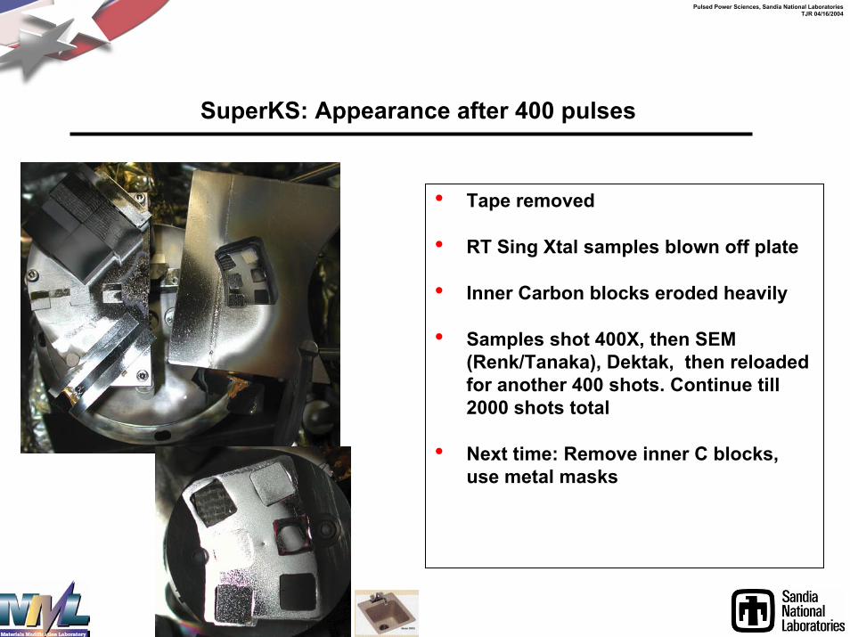
SuperKS: Appearance after 400 pulses
• Tape removed
• RT Sing Xtal samples blown off plate
• Inner Carbon blocks eroded heavily
• Samples shot 400X, then SEM (Renk/Tanaka), Dektak, then reloaded for another 400 shots. Continue till 2000 shots total
• Next time: Remove inner C blocks, use metal masks

Optical Micrographs, surfaces after 400 pulses (nitrogen)
Pulsed Power Sciences, Sandia National Laboratories
TJR 11/25/03
PMW, 1.5 J/cm2 (3000K), 520C W25Re, 1.5 J/cm2, 520C SingXtal W, 1.1 J/cm2 (2450K), 520C
PMW, 1.1 J/cm2 (1700K), RT Re, 1.2 J/cm2 (1800K), RT R6650 Graphite, 1.2 J/cm2, 520C

Heated W, W25Re, SingXtal smooth except for ‘exfoliation cracks’
Pulsed Power Sciences, Sandia National Laboratories
TJR 11/25/03
PMW, 1.2 J/cm2, 520C, 750Mag W25Re, 1.2 J/cm2, 520C, 2000Mag
SingXtal W, 1.2 J/cm2, 520C. 750Mag and 2000Mag
EDS in all cracks shows no contamination
Re, 2 J/cm2, RT, 2000MAG(Comparison) Re, 1.2 J/cm2, RT
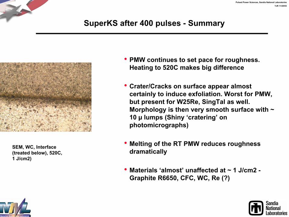
SuperKS after 400 pulses - Summary
Pulsed Power Sciences, Sandia National Laboratories
TJR 11/25/03
• PMW continues to set pace for roughness. Heating to 520C makes big difference
• Crater/Cracks on surface appear almost certainly to induce exfoliation. Worst for PMW, but present for W25Re, SingTal as well. Morphology is then very smooth surface with ~ 10 µ lumps (Shiny ‘cratering’ on photomicrographs)
• Melting of the RT PMW reduces roughness dramatically
• Materials ‘almost’ unaffected at ~ 1 J/cm2 -Graphite R6650, CFC, WC, Re (?)
SEM, WC, Interface (treated below), 520C, 1 J/cm2)

X-rays and ions deposit energy with different spatial profiles
photoelectric absorption of photons
photons removed from flux
I decreases exponentially
absorption length R = (µρ)-1
penetrates beyond R
I
X-rays (keV)
Rion collisions with electrons
ions slow down continuously
|-∂E/∂x| increases to Bragg peak
range is R
essentially no penetration beyond R
-∂E/∂x
Ions (∼MeV)
R

Materials response testing should accurately reproduce specific energy deposition in candidate materials
Need to reproduce:
(1) specific energy deposition S = ∆E/∆V ∼ F(J/cm2)/R(g/cm2)(2) temporal profile S(t) [∂S/∂t, pulse width,…)
rate of rise competes with thermal conductivity(3) spatial profile S(x) [deposition profile,…]
deposition scale length compared to grain size, impurity scale size,…
temperature gradients in deposition region
Z and RHEPP can replicate the conditions in IFE chamber walls• Though there are some differences between IFE target spectra and Z and RHEPP, the experiments study the most important issues• The surface temperature histories and temperature profiles are similar
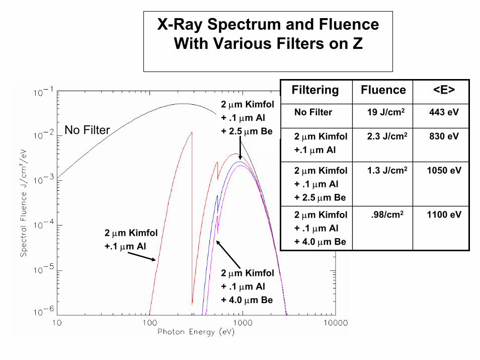
X-Ray Spectrum and Fluence With Various Filters on Z
1100 eV.98/cm22 µm Kimfol+ .1 µm Al + 4.0 µm Be
1050 eV1.3 J/cm22 µm Kimfol+ .1 µm Al + 2.5 µm Be
830 eV2.3 J/cm22 µm Kimfol+.1 µm Al
443 eV19 J/cm2No Filter
<E>FluenceFiltering
No Filter
2 µm Kimfol+.1 µm Al
2 µm Kimfol+ .1 µm Al + 4.0 µm Be
2 µm Kimfol+ .1 µm Al + 2.5 µm Be