rgo technical note 117 ccd camera eev #12 technical note 117 ccd camera eev #12 simon tulloch. 17...
TRANSCRIPT

Simon Tulloch RGO June 1998
1
RGO Technical Note 117 CCD Camera EEV #12
Simon Tulloch. 17 June 1998

Simon Tulloch RGO June 1998
2
CONTENTS
1. General Description.
2. Operational Modes.
3. Image Quality.
3.1. Defective Columns.
3.2. Hot Spots.
3.3. Pixel Response Non-Uniformity.
3.4. Point Spread Function.
4. Readout Noise and Readout Times.
5. Charge Transfer Efficiency.
6. Linearity and Full-Well.
7. Mechanical Parameters.
7.1. Device Flatness.
7.2. Focus Distance.
Appendices.
A. CCD Controller Configuration ListingB. Hardware Modifications to CCD ControllerC. Operating Voltages
Simon Tulloch RGO June 1998
3
1. General Description.
CCD Device Number A5500-5CCD Device Type EEV4280. Thinned and AR Coated.13.5µm pixels. 2148 x 4128 Pixels total. 50 x-underscan, 50 x-overscan, 28 y-overscan.Two working amplifiers, 4 and 5 electrons RMS noise.Cosmetically clean with 1 bright column only.QE=65% at 380nm, 81% at 400nm, 80% at 650nm, 14% at 950nm.Dark current= 0.75e/hour at -120C.Full Well= 240,000 electrons
2. Operational Modes.
The EEV42-80 devices have an on-chip gain switch that can reduce output node sensitivity by a factorof approximately 2.8. The default state is hi-sensitivity mode which minimises readout noise and givesan output sensitivity of about 4.5µV / electron. This mode is recommended for spectroscopicapplications. Lo-sensitivity mode can be selected at the CCD engineering terminal (see below) andallows the full dynamic range of the CCD to be utilised. In this mode, which is recommended forprime focus imaging, the CCD full-well signal matches closely the input range of the ADC. Readoutnoise rises to approximately 10e RMS but in most direct imaging applications this will beinsignificant next to sky noise.
To select Hi-Gain Mode (default) type : ‘hopg’To select Lo-Gain Mode (default) type : ‘lopg’To read back Mode setting type : ‘see’
An Anti-Blooming (AB) operational mode is also implemented for this camera although the defaultstate has it switched off. When enabled (see below) the vertical clock phases 1 and 2 are modulated sothat the integrated charge in each pixel is ‘wobbled’ back and forth. Excess charge that wouldotherwise produce a bloomed feature is removed by this process, which is thought to involve theinjection of holes from the CCD channel stops. Each ‘wobble’ cycle can remove >200 electrons. Thewobble frequency used for this device was 330 Hz. The drawback of AB clocks is that a large number(>4500) of bright spot features are generated in the image. One very bright saturated LED type defectis also created close to the left hand amplifier. Due to these drawbacks, the use of AB mode is notreally recommended for scientific imaging.
To switch AB clocks on type at the engineering terminal : 1 VHT ‘ANTI-BLOOM C!
To switch off : 0 VHT ‘ANTI-BLOOM C!
To check present setting : VHT ‘ANTI-BLOOM C?

Simon Tulloch RGO June 1998
4
3. Image Quality.Image quality was assessed from a series of five 600s dark frames. These were combined into oneimage using the IRAF ‘imcombine’ function with parameter ‘reject’ set equal to ‘minmax’ in order toreject cosmic ray features. Bright columns were then located by manual inspection of the resultantimage. The IRAF functions ‘daofind’ and ‘daophot’ were then used to log isolated ‘hot’ pixels. Thelocations of the defects recorded in this section have co-ordinates referenced to the left hand CCDamplifier.
Measurement temperature was -120C.
3.1. Defective Columns.
A bright feature near the top right of the image spills charge down column 1376. A trap cluster justvisible on the top left of the image blocks all signal that is vertically transferred through it.
600 second dark frame

Simon Tulloch RGO June 1998
5
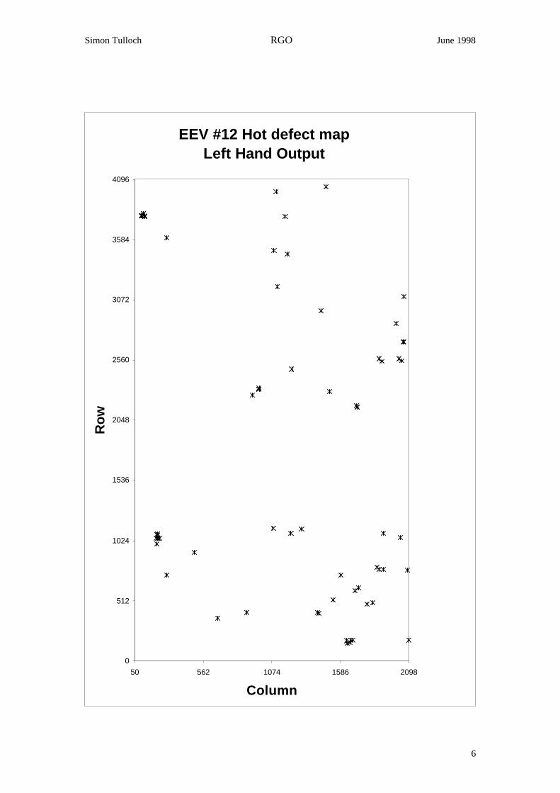
3.2. Hot Spots.The size and location , referenced to the left hand CCD amplifier, of significant hot spots is tabulatedbelow and shown graphically on the following page.
electrons electrons electrons electronsX-Coord Y-Coord after 600s after 300s X-Coord Y-Coord after 600s after 300s
1640 150 612 345 979 2321 84 411660 158 232 133 1222 2481 171 861633 172 122 56 1897 2548 125 1302098 178 195 128 2043 2553 80 251665 180 4605 2296 1876 2570 150 1031679 180 376 128 2023 2570 90 20668 366 288 182 2057 2715 667 342
1428 407 248 186 2060 2715 512 2341418 416 455 67 2003 2872 207 129884 417 179 460 1441 2979 806 417
1788 486 142 238 2062 3100 23273 115211827 501 217 142 1116 3186 22 381535 522 169 237 1190 3465 409 1821695 602 205 210 1088 3495 60 481723 628 332 374 290 3604 368 171286 735 74 0 122 3779 23726 11871
1591 736 186 234 123 3779 21432 107392089 778 103 43 1177 3782 97 491878 779 145 102 102 3785 3097 14821907 779 1110 465 100 3788 9204 46601860 798 211 116 104 3788 4838 2291495 926 931 434 123 3788 1672 835211 999 1022 445 113 3804 2506 1156211 1043 162 62 116 3804 2654 1224219 1047 180 92 1107 3992 919 427226 1047 628 334 1482 4031 3607 1718233 1047 450 252 1376 3811 >240000 >240000
2035 1052 292 197219 1073 4672 2283214 1077 141 111217 1084 2221 1112220 1083 4474 2240
1216 1088 319 1181910 1091 184 1121296 1126 185 1601087 1131 200 2051710 2161 245 1731715 2161 1525 8091707 2172 2802 1423927 2262 691 349
1507 2292 261 286979 2310 943 465979 2317 465 174
In addition to these hot spots , a sea level cosmic ray flux of 1940 events per hour was measured (2.2events cm-2 min-1).
Simon Tulloch RGO June 1998
6
EEV #12 Hot defect mapLeft Hand Output
0
512
1024
1536
2048
2560
3072
3584
4096
50 562 1074 1586 2098
Column
Ro
w

Simon Tulloch RGO June 1998
7
3.3. Pixel Response Non-Uniformity (PRNU).
This was measured at three wavelengths using the RGO flat field projector. The exposures weresufficiently deep to reduce photon noise below 0.2% , thus revealing the intrinsic pixel-pixelsensitivity variations. A cross-hatch pattern was visible in the 390nm exposures, thought to be due tolaser annealing. The sensitivity variation here was +/- 2%. At longer wavelengths this patterningdisappeared and the PRNU dropped to +/- 1%.
-3
-2
-1
0
1
2
3
4
0 100 200 300 400 500
-2.5
-2
-1.5
-1
-0.5
0
0.5
1
1.5
2
2.5
0 100 200 300 400 500
-3
-2
-1
0
1
2
3
0 100 200 300 400 500
390nm
565nm
950nm
%V
aria
tion
%V
aria
tion
%V
aria
tion
Column
Column
Column

Simon Tulloch RGO June 1998
8
3.4. Point Spread Function.
This was measured at two wavelengths using an optical device developed at RGO. This device used anall reflective microscope objective, pinhole and LED to project a 2µm diameter spot onto the CCD.The position of this spot could be adjusted to high precision using an X-Y translation stage. Focusingwas achieved by tilting the CCD slightly with respect to the X-Y plane in which the scan head moved.The spot was then scanned down a column of the CCD during integration , thus drawing out a lineimage. As the spot moved first towards and then away from best focus, the width of this scan linecould be seen to reach a minimum. It was thus possible to window in on a few hundred image rowsclose to this minimum where optimum focus was to be found. The X and Y axes of the translationstages were only approximately aligned to the rows and columns of the CCD. As the line image wasscanned out down a column, there would therefore be a small component of motion along the row axisof the chip. By examining consecutive rows of the line image (close to the optimum focus position) itwas then possible to measure the optical properties of the CCD at differing intra-pixel spot positions.Each line image therefore contained a great deal of information. An alternative, and very much morecomplex method would be to record several hundred individual spot images, stepping the position ofthe spot very slightly between each.
Line images were recorded at two wavelengths and the results are shown below. The CCD showedexcellent spatial resolution, at least compared to Lesser thinned Loral devices.
1
1.1
1.2
1.3
1.4
1.5
1.6
1.7
0 0.5 1 1.5 2
Spot position within pixel
FW
HM
(P
ixel
s)
1
1.1
1.2
1.3
1.4
1.5
1.6
0 0.5 1
Spot Position within Pixel
FW
HM
(P
ixel
s)
Pixe
l Cen
tre
Pixe
l Bou
ndar
y
Pixe
l Cen
tre
Pixe
l Cen
tre
Pixe
l Bou
ndar
y
Pixe
l Cen
tre
470nm
565nm
Simon Tulloch RGO June 1998
9
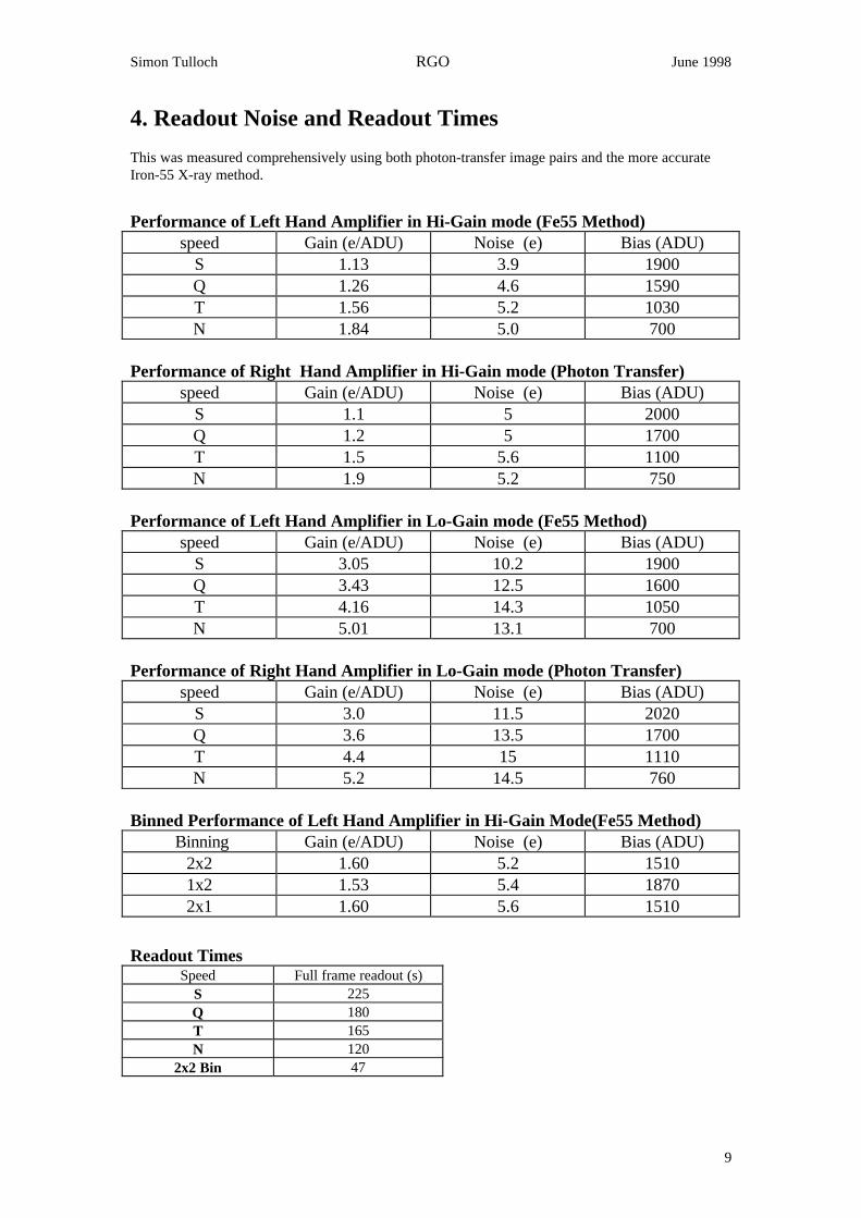
4. Readout Noise and Readout Times
This was measured comprehensively using both photon-transfer image pairs and the more accurateIron-55 X-ray method.
Performance of Left Hand Amplifier in Hi-Gain mode (Fe55 Method)speed Gain (e/ADU) Noise (e) Bias (ADU)
S 1.13 3.9 1900Q 1.26 4.6 1590T 1.56 5.2 1030N 1.84 5.0 700
Performance of Right Hand Amplifier in Hi-Gain mode (Photon Transfer)speed Gain (e/ADU) Noise (e) Bias (ADU)
S 1.1 5 2000Q 1.2 5 1700T 1.5 5.6 1100N 1.9 5.2 750
Performance of Left Hand Amplifier in Lo-Gain mode (Fe55 Method)speed Gain (e/ADU) Noise (e) Bias (ADU)
S 3.05 10.2 1900Q 3.43 12.5 1600T 4.16 14.3 1050N 5.01 13.1 700
Performance of Right Hand Amplifier in Lo-Gain mode (Photon Transfer)speed Gain (e/ADU) Noise (e) Bias (ADU)
S 3.0 11.5 2020Q 3.6 13.5 1700T 4.4 15 1110N 5.2 14.5 760
Binned Performance of Left Hand Amplifier in Hi-Gain Mode(Fe55 Method) Binning Gain (e/ADU) Noise (e) Bias (ADU)
2x2 1.60 5.2 15101x2 1.53 5.4 18702x1 1.60 5.6 1510
Readout TimesSpeed Full frame readout (s)
S 225Q 180T 165N 120
2x2 Bin 47

Simon Tulloch RGO June 1998
10
5. Charge Transfer Efficiency.
This was measured for low charge levels (1620e-) using Iron-55 X-rays, and for higher levels close tofull-well, using the Extended Pixel Edge Response technique. The results are tabulated below.
VCTE Fe55 (1620e-) 0.999998HCTE Fe55 (1620e-) 0.999998
VCTE 200,000e- 0.999997HCTE 200,000e- 0.9999987
Measurement temperature=-120C
Plots of the x-ray event pixel values along the horizontal and vertical image axes are shown below.

Simon Tulloch RGO June 1998
11
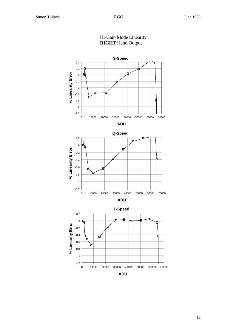
6. Linearity and Full-Well.
These characteristics were measured using a highly linear pulsed light source developed at RGO.
Hi-Gain Mode LinearityLEFT Hand Output
S-Speed
-1.2
-1
-0.8
-0.6
-0.4
-0.2
0
0.2
0 10000 20000 30000 40000 50000 60000 70000
ADU
% L
inea
rity
Err
or
Q-Speed
-1.2
-1
-0.8
-0.6
-0.4
-0.2
0
0.2
0 10000 20000 30000 40000 50000 60000 70000
ADU
% L
inea
rity
Err
or
T-Speed
-1.2
-1
-0.8
-0.6
-0.4
-0.2
0
0.2
0 10000 20000 30000 40000 50000 60000 70000
ADU
% L
inea
rity
Err
or
Simon Tulloch RGO June 1998
12
Hi-Gain Mode LinearityRIGHT Hand Output
T-Speed
-1.2
-1
-0.8
-0.6
-0.4
-0.2
0
0.2
0 10000 20000 30000 40000 50000 60000 70000
ADU
% L
inea
rity
Err
or
S-Speed
-1.2
-1
-0.8
-0.6
-0.4
-0.2
0
0.2
0.4
0 10000 20000 30000 40000 50000 60000 70000
ADU
% L
inea
rity
Err
or
Q-Speed
-1.2
-1
-0.8
-0.6
-0.4
-0.2
0
0.2
0 10000 20000 30000 40000 50000 60000 70000
ADU
% L
inea
rity
Err
or

Simon Tulloch RGO June 1998
13
T-Speed
-5
-4
-3
-2
-1
0
1
0 10000 20000 30000 40000 50000 60000
ADU
% L
inea
rity
Err
or
Q-Speed
-3.5
-3
-2.5
-2
-1.5
-1
-0.5
0
0.5
1
0 10000 20000 30000 40000 50000 60000 70000
ADU
% L
inea
rity
Err
or
Lo-Gain Mode LinearityLEFT Hand Output
Full Well

Simon Tulloch RGO June 1998
14
Lo-Gain Mode LinearityRIGHT Hand Output
Full Well
Q-Speed
-3.5
-3
-2.5
-2
-1.5
-1
-0.5
0
0.5
1
0 10000 20000 30000 40000 50000 60000 70000
ADU
% L
inea
rity
Err
or
T-Speed
-5
-4
-3
-2
-1
0
1
0 10000 20000 30000 40000 50000 60000
ADU
% L
inea
rity
Err
or

Simon Tulloch RGO June 1998
15
Binning Mode LinearityLEFT Hand Output, Hi-gain
2x2 Binning
-2
-1.5
-1
-0.5
0
0.5
0 10000 20000 30000 40000 50000 60000 70000
ADU
% L
inea
rity
Err
or
2x1 Binning
-1.2
-1
-0.8
-0.6
-0.4
-0.2
0
0.2
0.4
0 10000 20000 30000 40000 50000 60000 70000
ADU
% L
inea
rity
Err
or
1x2 Binning
-1.2
-1
-0.8
-0.6
-0.4
-0.2
0
0.2
0 10000 20000 30000 40000 50000 60000 70000
ADU
% L
inea
rity
Err
or

Simon Tulloch RGO June 1998
16
7. Mechanical Parameters.
The flatness of the CCD was measured using the RGO coplanarity scanner. The distance of the CCDbehind the cryostat window was measured using a travelling microscope.
7.1. Device Flatness.The CCD was extremely flat. The following plot shows a height data from a measurement scan downthe long axis of the CCD close to the central column.
-4
-3
-2
-1
0
1
2
3
4
0 500 1000 1500 2000 2500 3000 3500 4000
Row Number
Hei
ght (
Mic
rons
)
7.2. Focus Distance.
7.29 mm
4 mm
10.0 mmMeasured Optically
Window
CCD
focalplane

Simon Tulloch RGO June 1998
17
Simon Tulloch RGO June 1998
18
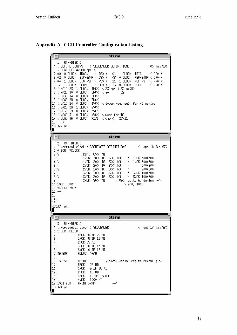
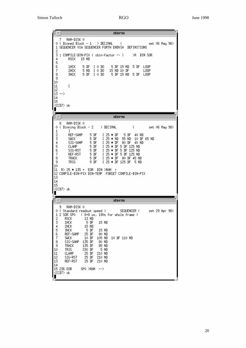
Appendix A. CCD Controller Configuration Listing.

Simon Tulloch RGO June 1998
19
Simon Tulloch RGO June 1998
20

Simon Tulloch RGO June 1998
21

Simon Tulloch RGO June 1998
22

Simon Tulloch RGO June 1998
23

Simon Tulloch RGO June 1998
24
Appendix B. Hardware Modifications to CCD Controller.The CDS time constant was set to 4µs . This was achieved by setting C8 and C7 =6.6nF and R12 andR13 =620 Ohms. R5 on the CDS card was set to 50K. Pre-amp resistors R31,32,33,34 all had 4K7resistors soldered in parallel to reduce gain. The corresponding electronic gain of the controller is asfollows :
Readout Speed Voltage GainS 29.8Q 26.9T 21.6N 18.3
Appendix C. Operating Voltages.