rf60 s oftware p rogramming g ui de 1. … s oftware p rogramming g ui de 1. purpose an370 v1.1 this...
TRANSCRIPT

Tel: +86‐755‐82973805 Fax: +86‐755‐82973550 E‐mail: [email protected] http://www.hoperf.com
RF60 S OF TWARE P ROGRAMMING G UI DE
1. Purpose
AN370 V1.1
This document defines the Application Programming Interface (API) for the RF60 firmware. It is intended to serve as a guide for application development. The document is related to the ROM version 0x0200 as returned by wSys_GetRomId() function and device revision 0x01 as returned by bSys_GetRevId() function. It describes files needed to build customer application and the details of the implemented API functions in ROM.
2. Known Issues
These are known issues related to the current version of the RF60 device, ROM version 0x0200 as returned by wSys_GetRomId() function and device hardware revision 0x01 as returned by bSys_GetRevId() function. „ There is an issue related to the LED driver, which demonstrates itself only under the following
circumstances when all 3 conditions are satisfied: z The device programming level is Factory or User. For those levels the C2 debugging interface is enabled after the boot by
a boot routine. z The device has been disconnected from the IDE. The "disconnected" means in a software sense, not physically, using
the Connect/Disconnect buttons on IDE. Or, the device is running the User code automatically after the boot without ever being connected to the IDE.
z The device is running a code which turns the LED on and off. If all the conditions are satisfied then after the first LED blink when the LED is turned off the GPIO4 stops working and is no longer visible to the application. If the device programming level is Run or the C2 debugging interface is internally disabled there is no issue. The LED can be turned on and off without affecting the device GPIO4 functionality. The issue can be summarized as follows: Whenever the C2 debugging interface is enabled, the device is not connected to IDE, and the LED is turned on and off, then the GPIO4 will stop functioning. Since in Run mode the C2 is disabled after the boot process finishes, the GPIO4 is not affected. Therefore, this issue only effects software development process and inconveniences the developer. After the application is finalized and the chip is programmed as Run there is no issue. See suggested solution scenarios and workarounds in the section related to debugging with LED.
1

Tel: +86‐755‐82973805 Fax: +86‐755‐82973550 E‐mail: [email protected] http://www.hoperf.com
AN370
TABLE OF C ONTENTS Section Page
1. Purpose . . . . . . . . . . . . . . . . . . . . . . . . . . . . . . . . . . . . . . . . . . . . . . . . . . . . . . . . . . . . . . . . . 1 2. Known Issues . . . . . . . . . . . . . . . . . . . . . . . . . . . . . . . . . . . . . . . . . . . . . . . . . . . . . . . . . . . . 1 3. Memory Regions . . . . . . . . . . . . . . . . . . . . . . . . . . . . . . . . . . . . . . . . . . . . . . . . . . . . . . . . . 4
3.1. 8051 Internal Memory . . . . . . . . . . . . . . . . . . . . . . . . . . . . . . . . . . . . . . . . . . . . . . . . . 5 3.2. Memory Map . . . . . . . . . . . . . . . . . . . . . . . . . . . . . . . . . . . . . . . . . . . . . . . . . . . . . . . . 5 3.3. CODE/XDATA RAM Reserved Area . . . . . . . . . . . . . . . . . . . . . . . . . . . . . . . . . . . . . . 6 3.4. DATA/IDATA Internal Memory Reserved Area . . . . . . . . . . . . . . . . . . . . . . . . . . . . . . 6
4. Building an Application . . . . . . . . . . . . . . . . . . . . . . . . . . . . . . . . . . . . . . . . . . . . . . . . . . . . 8 4.1. Type Definitions . . . . . . . . . . . . . . . . . . . . . . . . . . . . . . . . . . . . . . . . . . . . . . . . . . . . .8 4.2. Naming . . . . . . . . . . . . . . . . . . . . . . . . . . . . . . . . . . . . . . . . . . . . . . . . . . . . . . . . . . . . 8 4.3. Included Library Routines . . . . . . . . . . . . . . . . . . . . . . . . . . . . . . . . . . . . . . . . . . . . . 10 4.4. Stack Size Requirements . . . . . . . . . . . . . . . . . . . . . . . . . . . . . . . . . . . . . . . . . . . . . 11 4.5. Hardware Thread Safety . . . . . . . . . . . . . . . . . . . . . . . . . . . . . . . . . . . . . . . . . . . . . . 13 4.6. Non-ISR Functions . . . . . . . . . . . . . . . . . . . . . . . . . . . . . . . . . . . . . . . . . . . . . . . . . . 13 4.7. Function Calling Convention . . . . . . . . . . . . . . . . . . . . . . . . . . . . . . . . . . . . . . . . . . . 13 4.8. Files Needed for Building an Application . . . . . . . . . . . . . . . . . . . . . . . . . . . . . . . . . 14 4.9. Compiling an Application . . . . . . . . . . . . . . . . . . . . . . . . . . . . . . . . . . . . . . . . . . . . . . 16
5. User Application Required Interrupt Service Routines . . . . . . . . . . . . . . . . . . . . . . . . . 18 6. Interrupt and System Impact of Some Functions . . . . . . . . . . . . . . . . . . . . . . . . . . . . . . 20
6.1. Interrupt Enable Control . . . . . . . . . . . . . . . . . . . . . . . . . . . . . . . . . . . . . . . . . . . . . . 20 6.2. System Clock Control . . . . . . . . . . . . . . . . . . . . . . . . . . . . . . . . . . . . . . . . . . . . . . . . 21 6.3. Transmission Chain Control . . . . . . . . . . . . . . . . . . . . . . . . . . . . . . . . . . . . . . . . . . . 22
7. Module Descriptions . . . . . . . . . . . . . . . . . . . . . . . . . . . . . . . . . . . . . . . . . . . . . . . . . . . . . 22 7.1. AES Module . . . . . . . . . . . . . . . . . . . . . . . . . . . . . . . . . . . . . . . . . . . . . . . . . . . . . . . 22 7.2. Button Service Module and Master Time . . . . . . . . . . . . . . . . . . . . . . . . . . . . . . . . . 25 7.3. Demodulator Temperature Sensor Module . . . . . . . . . . . . . . . . . . . . . . . . . . . . . . . . 36 7.4. Encoding Module . . . . . . . . . . . . . . . . . . . . . . . . . . . . . . . . . . . . . . . . . . . . . . . . . . . 44 7.5. Frequency Counter Module . . . . . . . . . . . . . . . . . . . . . . . . . . . . . . . . . . . . . . . . . . . . 49 7.6. Frequency Casting Module . . . . . . . . . . . . . . . . . . . . . . . . . . . . . . . . . . . . . . . . . . . . 52 7.7. HVRAM Module . . . . . . . . . . . . . . . . . . . . . . . . . . . . . . . . . . . . . . . . . . . . . . . . . . . . 56 7.8. Multi Time Programmable (MTP) Memory Module . . . . . . . . . . . . . . . . . . . . . . . . . 57 7.9. Battery Voltage Measurement Module . . . . . . . . . . . . . . . . . . . . . . . . . . . . . . . . . . . 63 7.10. Non-Volatile Memory (NVM) Copy Module . . . . . . . . . . . . . . . . . . . . . . . . . . . . . . . 65 7.11. Output Data Serializer (ODS) Module . . . . . . . . . . . . . . . . . . . . . . . . . . . . . . . . . . . 70 7.12. Power Amplifier (PA) Module . . . . . . . . . . . . . . . . . . . . . . . . . . . . . . . . . . . . . . . . . 73 7.13. Single Transmission Loop (STL) Module . . . . . . . . . . . . . . . . . . . . . . . . . . . . . . . . 76 7.14. System Module . . . . . . . . . . . . . . . . . . . . . . . . . . . . . . . . . . . . . . . . . . . . . . . . . . . . 81 7.15. Sleep Timer Module . . . . . . . . . . . . . . . . . . . . . . . . . . . . . . . . . . . . . . . . . . . . . . . . 92
8. Simple Application Example . . . . . . . . . . . . . . . . . . . . . . . . . . . . . . . . . . . . . . . . . . . . . . . 95 Contact Information . . . . . . . . . . . . . . . . . . . . . . . . . . . . . . . . . . . . . . . . . . . . . . . . . . . . . . . . 99

Tel: +86‐755‐82973805 Fax: +86‐755‐82973550 E‐mail: [email protected] http://www.hoperf.com
AN370
3. Memory Regions The following table lists some key terms for writing firmware for the RF60:
Term Definition
8051 Internal Memory
256 bytes of RAM internal to the 8051 MCU. Fastest for MCU to access. It is broken into three categories, DATA, IDATA and SFR space. See below for a description of these.
DATA Portion of the internal memory at addresses 0x00 through 0x7F. This memory can be accessed both directly and indirectly. DATA is a recognized Keil compiler keyword.
IDATA Portion of the internal memory occupying addresses 0x80 through 0xFF. This memory can only be accessed indirectly. IDATA is a recognized Keil compiler keyword.
SFR Space Special Function Register Space is located in internal memory at addresses 0x80 through 0xFF. This memory can only be accessed directly.
CODE XDATA
This is both user code memory (CODE) and external data memory (XDATA). Residing at addresses 0x0000 through 0x11FF. In the RF60 this space is equivalent to the 4.5 kB of on chip RAM. CODE/XDATA RAM is where the user application is run from. CODE and XDATA are recognized Keil compiler keywords.
XREG Refers to the set of hardware registers located in XDATA address space at addresses 0x4000 through 0x40FF. More information on XREGs can be found in the RF60 datasheet. This is not a recognized Keil compiler keyword.
ROM Read only memory containing all the API functions. Residing at CODE addresses 0x8000 through 0xAFFF. The CPU executes ROM code directly. ROM in not readable by the user application.
NVM Non-Volatile Memory. Each bit can only be written as 1 once (One Time Programmable, OTP). Code stored in this memory is intended to be loaded into RAM upon boot. It is also possible for the application to copy code from NVM using the NVM Copy Module when using overlays. Virtually mapped to addresses 0xE000 through 0xFFFF. Not directly acces- sible by MCU. Only accessible by special hardware using API functions. Only formatted data programmed by the NVM composer/programmer are available to be loaded at boot time or at runtime by bNvm_CopyBlock() function. There is not byte by byte direct access to NVM.
MTP 128 bits of Multi-Time Programmable Memory (EEPROM). This memory is mapped as read only at XDATA addresses 0x4040 to 0x404F. Writing to MTP can only be done through the MTP API Module. User should use the MTP API for read access as well.
3

Tel: +86‐755‐82973805 Fax: +86‐755‐82973550 E‐mail: [email protected] http://www.hoperf.com
AN370
DATA
SFR (DATA)
XREG
64K
B
16K
B
3.1. 8051 Internal Memory Figure 1 shows the RF60 memory which is internal to the 8051 MCU.
Internal Memory
Both direct and indirect addressing
0x00
0x7F 0x80
0xFF
IDATA
0x80 0xFF
Direct addressing only MOV A, addr
Indirect addressing only by @Ri pointers MOV A, @Ri
3.2. Memory Map
Figure 1. CPU Internal Memory Organization
After the chip boots, the memory on the RF60 is mapped as shown in Figure 2. The 4.5 kB RAM section is accessible both as CODE and XDATA (MOVC and MOVX instructions). The XREG region is accessible only as XDATA (MOVX). The ROM is not accessible as data, but the code residing in ROM can be executed. The NVM is virtually mapped into this region, but is not directly accessible by CPU. The NVM API functions must be used to access the NVM.
CODE/ XDATA
0x0000
0x11FF
RAM 4.5K
0x4000 0x40FF
0x8000
0xAFFF
ROM 12K
0xE000
0xFFFF
NVM 8K
Virtual mapping, not directly accessible by CPU
Figure 2. RF60 Unified CODE/XDATA Memory Organization
4

Tel: +86‐755‐82973805 Fax: +86‐755‐82973550 E‐mail: [email protected] http://www.hoperf.com
A N370
Boot_AfterTrimExe
Boot_PatchExe
Boot
XD
ATA
3.3. CODE/XDATA RAM Reserved Area ROM API code uses at least 304 bytes (0x130) of CODE/XDATA space at the end of the RAM (highest addresses). This area must not be used by the application. The following diagram gives an outline of the used space. The area used by the API and other factory settings may change dynamically per chip. The user should read the value of the wBoot_DpramTrimBeg variable, which points to the first used address in the CODE/XDATA RAM. Any location at lower address then the one pointed to by the content of the wBoot_DpramTrimBeg variable is available for customer user. See the Boot section in the RF60 data sheet.
0x0000
CODE/XDAT A RAM 4.5KB
User CODE/ XDATA
Factory XDATA
0x11F3
0x11F5
wBoot_DpramTrimBeg
wBoot_NvmUserBeg
0x11F7
0x11FD wBoot_NvmCopyAddr
0x11FF bBoot_BootStat
Figure 3. CODE/XDTA RAM Organization
Important: The user application must not overwrite the Factory and Boot XDATA region during runtime. There is no hardware protection of that region, so it is up to the customer discipline not to place any CODE nor XDATA variables. If that happens, the behavior of the chip becomes unpredictable.
3.4. DATA/IDATA Internal Memory Reserved Area Portions of the 8051 MCU internal memory are also used by ROM API code. The following diagram shows DATA and IDATA used by ROM API code. The provided file RF60_link.c must be compiled and link with the application. The file contains dummy arrays at fixed addresses to notify the linker not to put any data into the reserved regions. The user must set the stack pointer such that the stack will never overwrite the reserved regions.
5

Tel: +86‐755‐82973805 Fax: +86‐755‐82973550 E‐mail: [email protected] http://www.hoperf.com
A N370
Reg RB0 Used by API
(8B) Registers
RB1 .. RB3Available
(24B)
Bit Addr Available
(16B)
API Reserved
(50B)
Available (31B)
DATA/IDATA
MCU Internal RAM
0x00
0x07 0x08
0x1F 0x20
0x2F 0x30
DATA .. lower 128 RAM bytes, Direct and Indirect Addressing
0x61 0x62
0x7F
0x80
0xDD 0xDE
0xFF
Available (94B)
API Reserved
(34B)
IDATA .. upper128 RAM bytes, Indirect Addressing only
Figure 4. DATA/IDATA Reserved Spaces
Note that the region used by the ROM API is split in between the DATA and IDATA to allow the continuous region of 128 bytes, split evenly in between DATA and IDATA regions. This will allow for a byte array of that size. The bit addressable region of 16 bytes is not used by the API. The register bank RB0 is shown as available. However, the user should assume that the API functions destroy all the registers R0 .. R7. API functions use the currently selected register bank by the user application. The API functions do not access the R0 .. R7 directly. User is free to choose any register bank for main application and any register bank for interrupt service routines.
6

Tel: +86‐755‐82973805 Fax: +86‐755‐82973550 E‐mail: [email protected] http://www.hoperf.com
A N370
4. Building an Application 4.1. Type Definitions The following table lists types that are defined or expected for use with the RF60 API. The custom types are defined in the header file RF60_types.h.
Type Bit Width Type Definition Prefix
unsigned char 8 BYTE b
unsigned int 16 WORD w
unsigned long int
32
LWORD
l
signed char
8
CHAR
c
int
16
i
long int
32
j
float
32
f
All variables are stored in big endian fashion, which means that the most significant byte is stored on the lowest (smallest) address location.
4.2. Naming Strict naming conventions are used for the API. Each function belonging to the same software module is prefixed by the module name or module name abbreviation. Before the module name, the function name is prefixed by the type of the return value. All variables are prefixed by their type. Defined types, pointers, input and output variables, and pointers to input/ output function variables are also prefixed accordingly. In addition to the prefixes for the basic types in the table in section 4.1, the following prefixes are used. The dot in the prefix specification means that the letter cannot stand on its own and must be preceded or succeeded by another prefix letter or letters:
Prefix Description Example
t Type definition of a structure tBsr_Setup
r Structure variable definition rSetup
p. Pointer to prSetup
v Void vBsr_Setup()
.i Input function variable biTstCtrl
..o Output function variable. Make sense if used as a pointer to output. The pointed content is generated by the function.
*pboOutput
..io Input/output function variables. Make sense if used as a pointer. The pointed content is used as input and modified by a function.
*pbioState
7

Tel: +86‐755‐82973805 Fax: +86‐755‐82973550 E‐mail: [email protected] http://www.hoperf.com
A N370
The module naming prefixes used are as follows:
Module Prefix Module Name
Aes AES
Bsr Button service routine
DmdTs Temperature sensor and its demodulator
Enc Encoding of data for transmission
Fc Frequency counter
FCast Frequency casting and fine tuning
Hvram HVRAM
Mtp MTP (EEPROM) memory
MVdd Battery VDD measurement
Nvm NVM memory for copying data to RAM
Ods Output data serializer
Pa Power amplifier
Sys System functions
SleepTim Sleep timer
Stl Single Tx loop
Example:
void vAes_Cipher /* AES 128 bit key encryption .. works on global IDATA State and RoundKey */
( BYTE idata *pbioState, BYTE idata *pbioRoundKey );
The function returns void (v) and is a part of the AES (Aes) module. It has two input pointer variables (p), both pointing into the DATA/IDATA internal memory at a BYTE (b). The area pointed to is both input to the function and is modified by the function (io).
8

Tel: +86‐755‐82973805 Fax: +86‐755‐82973550 E‐mail: [email protected] http://www.hoperf.com
A N370
4.3. Included Library Routines Following is a list of all Keil library routines included in ROM. They are available for use by the application via the ROM symbol map file for Keil toolchain (RF60_rom_keil.a51). The library routines cannot be used with other toolchains. If the user does not desire to link these library routines to the application (they take precedence over the actual library provided by the toolchain), then it is necessary to use RF60_rom_all.a51 instead of the Keil specific toolchain during the application building.
?C?ULSHR ?C?LSHL ?C?OFFXADD ?C?FPSUB ?C?FPADD ?C?FPMUL ?C?FCASTL ?C?FCASTC ?C?FCASTI ?C?CASTF ?C?FPGETOPN2 ?C?FPNANRESULT ?C?FPOVERFLOW ?C?FPRESULT ?C?FPRESULT2 ?C?FPUNDERFLOW ?C?LNEG ?C?LLDIDATA ?C?LLDXDATA ?C?LLDIDATA0 ?C?LLDXDATA0 ?C?LSTIDATA ?C?LSTXDATA ?C?LMUL ?C?ULCMP ?C?LOR ?C?LADD ?C?IMUL ?C?LSUB ?C?LXOR ?C?FPDIV ?C?ULDIV ?C?SIDIV ?C?PCMP3 ?C?FPCMP ?C?UIDIV ?C?SLDIV _ABS ?C?ICALL ?C?ICALL2 ?C?IILDX
9

Tel: +86‐755‐82973805 Fax: +86‐755‐82973550 E‐mail: [email protected] http://www.hoperf.com
A N370
4.4. Stack Size Requirements Table 1 shows the additional stack requirements when the user code is calling an API function. The number of bytes in the table is in addition to the 2 bytes return address storage requirements for the return address to be stored on top of the stack when the function is called. For example, if the function is not using any additional stack storage (not calling any other function, and not using PUSH/POP instructions), then the function internal stack requirement is listed as 0. The maximum stack size requirement is determined by the interrupt service routines and if the application is using one or two interrupt priorities. The worst case stack requirement would come from the application using two levels of interrupt levels and lower priority ISR was interrupted by the higher priority ISR. The user is required to leave at least additional 4 bytes of stack space, 2 bytes as a guard and 2 bytes for possible use in the future.
Table 1. Additional Stack Requirements
Function Internal stack use [bytes]
vAes_Cipher 3 vAes_InvCipher 3 vAes_InvGenKey 3
wBsr_Pop — vBsr_Setup 4 vBsr_InitPts 2
bBsr_GetPtsItemCnt — vBsr_Service 4
wBsr_GetCurrentButton — bBsr_GetTimestamp 2
vDmdTs_Setup — iDmdTs_GetData —
iDmdTs_GetLatestDmdSample — iDmdTs_GetLatestTemp 2
vDmdTs_ClearDmd — vDmdTs_ClearDmdIntFlag —
vDmdTs_IsrCall 2 bDmdTs_GetSamplesTaken —
vDmdTs_Enable — vDmdTs_RunForTemp 2 vDmdTs_ResetCounts —
bEnc_4b5bEncode — vEnc_Set4b5bLastBit —
bEnc_ManchesterEncode — vFCast_Setup — vFCast_XoSetup 4 vFCast_Tune 8
vFCast_FskAdj 4 vFCast_FineTune 4
vFc_Setup — vFc_StartCount —
vFc_PollDone — lFc_StartPollGetCount 2
lFc_GetCount —
10

Tel: +86‐755‐82973805 Fax: +86‐755‐82973550 E‐mail: [email protected] http://www.hoperf.com
A N370
Table 1. Additional Stack Requirements (Continued)
bHvram_Read — vHvram_Write —
lMtp_GetDecCount 2 vMtp_SetDecCount 6
vMtp_IncCount 2 bMtp_Write 2
pbMtp_Read 2 vMtp_Strobe —
iMVdd_Measure 6 vNvm_SetAddr —
wNvm_GetAddr — bNvm_CopyBlock —
vNvm_McEnableRead 2 vNvm_McDisableRead —
vOds_Setup — vOds_Enable — vOds_WriteData —
vPa_Setup 2 vPa_Tune 4
lSleepTim_GetCount 2 vSleepTim_SetCount 2
bSleepTim_CheckDutyCycle 4 vSleepTim_AddTxTimeToCounter 4
lSleepTim_GetOneHourValue — vStl_EncodeSetup — vStl_SingleTxLoop 6
vStl_PreLoop 6 vStl_PostLoop 2
bStl_EncodeByte 2 vSys_BandGapLdo 2
wSys_GetRomId — wSys_GetChipId —
bSys_GetRevId — lSys_GetProdId —
bSys_GetBootStatus — vSys_SetClkSys —
vSys_Setup — lSys_GetMasterTime 2 vSys_IncMasterTime 2
vSys_SetMasterTime — vSys_LedIntensity —
vSys_Shutdown 2 vSys_16BitDecLoop — vSys_8BitDecLoop — vSys_FirstPowerUp 4 wSys_GetKeilVer —
vSys_ForceLc 2 vSys_LpOscAdj 4
11

Tel: +86‐755‐82973805 Fax: +86‐755‐82973550 E‐mail: [email protected] http://www.hoperf.com
A N370
4.5. Hardware Thread Safety Almost all of the API functions access hardware. If the function accessing the same hardware is going to be used in the main application and in the interrupt service routine (ISR) then there is a conflict. There are no semaphores nor any hardware access protections implemented in the API routines. From hardware point of view, the API functions should be treated as not thread safe.
4.6. Non-ISR Functions Certain functions in the ROM are not allowed to be called from an interrupt service routine (ISR). This is because they share memory space (DATA, IDATA, XDATA) with other functions in the form of thier local variables. Sharing variables is a way to reduce the use of memory. The reason that calls from an interrupt service routine are not allowed is because of the possibility of two functions running at the same time which are relying on the same memory space. Following is a list of functions which may not be called from within any interrupt service routine.
vAes_Cipher() vAes_InvCipher() vAes_InvGenKey() wBsr_Pop() wBsr_GetCurrentButton() lMtp_DecToGray() lMtp_GetDecCount() vMtp_IncCount() vSleepTim_GetCount() vSleepTim_SetCount()
4.7. Function Calling Convention All input and output function variables are passed in registers. The function calling convention and parameter passing is a Keil convention. It is also used by Raisonance toolchain. Maximum 3 parameters can be passed to functions in registers. When more input data is needed within the function, a data structure is used and only a pointer to the structure is passed to the function. Generic pointers (3 byte pointer) are not used in the API and if the pointer is passed as an input to a function, the storage location where it points to is always specified. The table below shows the order of the function parameter and what registers store them. Note that unsigned types are passed the same way as signed (char and unsigned char, for example).
Argument Type and Passing Registers Argument Order
Number char or 1-byte pointer (*DATA, *IDATA)
int or 2-byte pointer (*XDATA)
long or float
1. R7 R6 .. MSB R7 .. LSB
R4-R7 (R4 .. MSB)
2. R5 R4 .. MSB R5 .. LSB
R4-R7 (R4 .. MSB)
3. R3 R2 .. MSB R3 .. LSB
N/A
12

Tel: +86‐755‐82973805 Fax: +86‐755‐82973550 E‐mail: [email protected] http://www.hoperf.com
A N370
If the registers required by subsequent parameters are taken by the previous arguments, then the subsequent arguments cannot be passed in the registers. For example, passing two long variables in registers is not possible. Similarly, passing long first and int second is not possible, while passing int first and long second is possible. Function return values are always passed in registers. Note that unsigned types are passed the same way as signed (char and unsigned char, for example).
Return Type Passing Registers
bit CY .. carry flag char or 1-byte pointer (*DATA, *IDATA)
R7
int or 2-byte pointer (*XDATA)
R6 .. MSB R7 .. LSB
long or float
R4–R7 (R4 .. MSB)
The user should also assume that all the functions are modifying all the registers in the current register bank. 4.8. Files Needed for Building an Application When building an application which will use ROM based API functions, there are several files needed. The following table lists these files along with their descriptions.
File Name Description
RF60_types.h Header file that declares type definitions used in the API. See TypeDefinitions section for more information.
RF60.h Device header file that declares all SFR and XREG registers. It also defines masks and bit indices which are to be used when accessing fields within registers. This is a C header file. Must be included in all C files using the RF60.
RF60.inc Same as RF60.h, but for use with an assembler. This file should be included in all assembly source files while using RF60.
RF60_api_rom.h C header declaring all the API functions. Must be included to the application which uses the API.
startup.a51 Simplified assembly startup file for Keil and Raisonance toolchains. Customer may want to modify this file. It must be included in the application build.
RF60_rom_keil.a51 Assembly ROM symbol map that must be assembled and linked into the application build if the API functions are being used. It tells the linker the API functions are located in ROM. This file is tailored to Keil toolchain. It also includes references to some of the Keil library functions.
13

Tel: +86‐755‐82973805 Fax: +86‐755‐82973550 E‐mail: [email protected] http://www.hoperf.com
A N370
File Name Description
RF60_rom_all.a51 Same as above, but for any other toolchain. It can also be used with Keil toolchain if the user does not desire to use Keil library functions in ROM. With Keil toolchain use either this one or the one above, but not both.
RF60_data.c Data file related to the RF60.h defining the XREG register in XDATA area. This file must be included in the application build.
RF60_link.c File with dummy array variables to force linker to avoid DATA and IDATA spaces used and reserved by ROM API. If this file is not used the linker area avoidance directive must be used. User may want to augment this file to notify the linker that the end of CODE/ XDATA RAM is also reserved for API use. A commented section showing how to achieve that is included at the end of the file.
RF60_fix_rom_keil.lib Keil library file containing fixed vFCast_FskAdj function. Without it the frequency modulation will not work.This file must be included in the application build if FSK modulation is used (i.e., vFCast_FskAdj function is called). In that case, only the Keil tool- chain is supported.
These files are in the directory:
…\common\src\
in the RF60 installation tree. 4.8.1. Device RF60.h and RF60.inc Headers The C device header RF60.h and assembly RF60.inc header define the hardware registers in the device. They define all the SFR, XDATA mapped XREG registers, boot status variables, and interrupt priority numbers. Same items are defined in both the C and assembly headers, so only the C header is used to describe what is present there. The same applies to the assembly device header. For each of the fields in each of the SFR or XREG registers there is a register address defined. However, if the byte wide register consists of more than one field which has a width less than 8 bits, there are two additional items defined for each field, mask and bit location. The mask field name has M_ prefix, while the bit index name has B_ prefix: 1. The bit mask for the field. The mask contains 1 at the bit positions within a byte occupied by the field: #define M_<FIELD NAME> <field bit mask> 2. The bit index number within the byte where the field begins. In other words, the base bit index of the field within
a byte: #define B_<FIELD NAME> <field low significant bit index> For example: /* -- ODS_TIMING .. 0xaa */
#define
#define
#define
M_ODS_CK_DIV
M_ODS_EDGE_TIME
M_ODS_GROUP_WIDTH
0x07
0x18
0xe0
.. field mask defines
#define
B_ODS_CK_DIV
0
.. base bit index defines
#define B_ODS_EDGE_TIME 3 #define B_ODS_GROUP_WIDTH 5
14

Tel: +86‐755‐82973805 Fax: +86‐755‐82973550 E‐mail: [email protected] http://www.hoperf.com
A N370
The #define statements were added for convenience to initialize or modify the single and multi-bit fields inside of the registers. For example if the user desires to initialize fields ODC_CK_DIV to 5, ODS_EDGE_TIME to 2, and ODS_GROUP_WIDTH to 6 in the ODS_TIMING register then in the usual manner the user would have to define the masks himself or use direct constants in the code:
ODS_TIMING = 5 | (2 << 3) | (6 << 5);
Hard to read what the intent was. Suggested way using the provided base bit constants is as follows: ODS_TIMING = (5 << B_ODS_CK_DIV)
| (2 << B_ODS_EDGE_TIME)
| (6 << B_ODS_GROUP_WIDTH);
To use this naming to clear the Matrix and Roff mode bits at the beginning of the user application, the code can be made very readable: /* Disable the Matrix and Roff modes on GPIO[3:1] */
PORT_CTRL &= ~(M_PORT_MATRIX | M_PORT_ROFF | M_PORT_STROBE);
PORT_CTRL |= M_PORT_STROBE;
PORT_CTRL &= (~M_PORT_STROBE);
4.9. Compiling an Application To use the RF60 API to build a user application in C, the user must do the following: 1. To be able to use the IDE for debugging, the user must use the Keil BL51 linker or toolchain with the standard
OMF-51 output file format. The user cannot use the LX51 linker, since the Keil proprietary output format, OMF-2, is not understood by the IDE.
2. Add the path …\common\src\ to the C compiler and include directive. This is where the RF60 files are installed.
3. Include RF60.h and RF60_api_rom.h headers in every C source file of the application. These files include the RF60_types.h header automatically:
#include "RF60.h" #include "RF60_api_rom.h"
4. Add the following files, which have to be assembled or compiled, into the application build, and/or those files must be linked with the user application:
RF60_rom_keil.a51 or for non-Keil compilers RF60_rom_all.a51 RF60_data.c RF60_link.c startup.a51 RF60_fix_rom_keil.lib
For Keil toolchain, if the user does not desire to use some of the Keil library functions in the ROM, then the file RF60_rom_all.a51 must be used with the Keil toolchain instead.
5. The user must use the stack pointer setting directive manually on a linker command line or from the compilation IDE. Since the end of the IDATA memory is reserved and used by the API, the stack segment for stack pointer setting as defined in startup.a51 must be done manually. Optionally, the startup.a51 can be modified not to include stack pointer setting using a stack segment. Then the user will have to set the stack pointer manually to a fixed location in startup.a51 or at the beginning of the application.
15

Tel: +86‐755‐82973805 Fax: +86‐755‐82973550 E‐mail: [email protected] http://www.hoperf.com
A N370
The following shows linker command line directives to place a stack manually using the address 0x80 as an example:
For Keil BL51: STACK(?STACK(0x80)) For Keil LX51: SEGMENTS(?STACK(I:0x80)) For Raisonance:IDATA(?STACK(0x80)) .. while using the supplied startup.a51
6. The user must make sure that the application is not using the CODE/XDATA reserved area of RAM as described above. To achieve this, the user may either control the XDATA reserved area directly on a linker command line, or edit the RF60_link.c file to add the reserved XDATA area there (preferred solution, since the file contains a commented section at its end explaining how to do that), or create additional file with dummy fixed address XDATA byte array.
7. The user must make sure that the CODE and XDATA areas as provided to the linker are not overlapping since the CODE and XDATA share the same physical RAM. For example, the CODE and XDATA linker directives should set as shown below. In this example, the code size is limited to 0x0D00 length, followed by XDATA variable area:
For Keil BL51: CO(0x0000-0x0CFF) XD(0x0D00-0x107F) For Keil LX51: CLASSES(CODE(C:0X0-C:0XCFF), CONST(C:0X0-C:0XCFF), XDATA (X:0XD00-X:0X107F), … )
8. The API uses part of both DATA/IDATA and XDATA memories for data storage and the user application code must not change content of those areas. Those areas must be completely avoided by the user application. The provided file RF60_link.c reserves API space in DATA/IDATA memories as used by API, since the API regions in DATA/IDATA memories are fixed.
However, the API routines occupy XDATA area towards the end of the XDATA space. The size of the API occupied region depends on the trim value and may change from chip to chip, but usually the value will be fixed for all production parts of the same revision.
At the end of the RF60_link.c file there is a commented out section how to tell the linker that the end of the CODE/XDATA memory is reserved for API use. The user should read the wBoot_DpramTrimBeg variable to get the first address of the API occupied location. Anything below that (towards 0x0000) is available for user CODE/ XDATA to use. The user has to look at the content of wBoot_DpramTrimBeg residing at the address 0x11F3. The variable content is directly accessible from the IDE:
View → Debug Windows → RF60 → System Vars
It is critical that neither user CODE nor user XDATA will encroach on that space.
For example, on the currently shipped ROM version 02.00 of the chip has the value
wBoot_DpramTrimBeg = 0x1080
Therefore, as an example, that user needs to reserve 64 bytes (0x40) of the XDATA space for his application and the rest of the CODE/XDATA memory will be reserved for code. It is recommended to keep the user XDATA after the CODE as shown in this example:
CODE: 0x0000 .. 0x103F XDATA: 0x1040 .. 0x107F … 64 bytes of XDATA just before the API XDATA
The linker directives as in the item 7 above would be as follows: For Keil BL51: CO(0x0-0x103F) XD(0x1040-0x107F) For Keil LX51: CLASSES(CODE(C:0x0-C:0x103F), CONST(C:0x0-C:0x103F), XDATA (X:0x1040-X:0x107F), … )
16

Tel: +86‐755‐82973805 Fax: +86‐755‐82973550 E‐mail: [email protected] http://www.hoperf.com
A N370
5. User Application Required Interrupt Service Routines
The device API and user application cannot function without the temperature sensor demodulator module running behind the scenes and measuring temperature. The same module is used when measuring battery voltage. For the system to be functional the user must include a temperature sensor demodulator interrupt service routine (DMD ISR) in the main application code. At least two DMD TS module calls must be included in the DMD ISR as shown in the example below. API functions relying on the DMD ISR to be present are: vFCast_Tune()
vSys_LpOscAdj()
vStl_PreLoop()
vStl_SingleTxLoop()
iMVdd_Measure()
All the functions from the DMD TS module with module prefix DmdTs_* also require the DMD ISR to be present in the system. The user is free to use the using directive when defining ISR functions. The downside of not using the using directive when defining an ISR is that when the ISR is invoked the system needs to store 13 bytes of data on the stack, on top of 2 bytes of the return address. Therefore, stack requirements are more pronounced if the using directive is not used. Required DMD ISR. The ISR must call two DMD TS functions as shown.
/*
*------------------------------------------------------------------------------
*
* INCLUDES:
*/
#include "RF60.h"
#include "RF60_api_rom.h" /*
*==============================================================================
*
* VISIBLE FUNCTIONS:
*/
void vIsr_Dmd
(
void
)
interrupt INTERRUPT_DMD using 1 /* Use RB1 for this ISR */
/*------------------------------------------------------------------------------
*
* FUNCTION DESCRIPTION:
* This is the interrupt service routine for the DMD. It clears the DMD
17

Tel: +86‐755‐82973805 Fax: +86‐755‐82973550 E‐mail: [email protected] http://www.hoperf.com
A N370
* interrupt flag and calls the vDmdTs_IsrCall() which handles the
* interface to the demodulator and temperature sensor.
*
*------------------------------------------------------------------------------
*/
{
/*
*------------------------------------------------------------------------------
*
* VARIABLES:
*
*------------------------------------------------------------------------------
*/ /* Clear the demodulator interrupt flag */
vDmdTs_ClearDmdIntFlag(); /* Call DMD TS function that handles skipping samples and getting the sample
* from the temperature sensor demodulator */
vDmdTs_IsrCall();
} /*
*------------------------------------------------------------------------------
*/
18

Tel: +86‐755‐82973805 Fax: +86‐755‐82973550 E‐mail: [email protected] http://www.hoperf.com
A N370
6. Interrupt and System Impact of Some Functions This section summarizes how functions impact interrupt enables, system clock settings, and key hardware blocks on the device. This information is provided such that the user will be able to consider the side effects of the API functions.
6.1. Interrupt Enable Control Only the temperature sensor demodulator interrupt enabled EDMD bit and the global interrupt enable bit EA are manipulated by the API functions. One of the functions clears the EODS as well. There are functions manipulating the EA and EDMD flags directly and then functions manipulating them indirectly by calling the direct manipulator functions. Table 2 shows what happens with each of the interrupt enables:
Table 2. Functions Summary
Function EA EDMD Notes Direct Functions
vDmdTs_RunForTemp 1 1 Force both interrupt flags to enable iDmdTs_GetLatestDmdSample S, 0, R — Disable interrupts during operation. They are
disabled only for a dozen clock cycles. vMtp_Strobe S, 0, R — Disable interrupts during operation. They are
disabled for about 4us. bMtp_Write S, X, R — Disable interrupts only around critical portions
of the code. See function description for details.
iMVdd_Measure S, 1, R 1, 0 Needs DMD TS interrupt service to run. It forcibly enables the DMD interrupt and then disables it. User needs to reenable the EDMD=1 if that was the previous state.
vStl_PostLoop — 0 It also forces EODS=0, but the ODS interrupt is not currently used by API.
Calling Direct Functions vFCast_Tune 1 1 From vDmdTs_RunForTemp vStl_PreLoop 1 1 From vDmdTs_RunForTemp vSys_LpOscAdj 1 1 From vDmdTs_RunForTemp iDmdTs_GetLatestTemp S, 0, R — From iDmdTs_GetLatestDmdSample pbMtp_Read S, 0, R — From vMtp_Strobe Notes:S, 0, R: Save the original value upon entry, force value to 0 for function processing, restore the original value
before return. S, 1, R: Save the original value upon entry, force value to 1 for function processing, restore the original value before return. S, X, R: Save the original value upon entry, force both 0 and 1 values during the function processing, restore the original value before return. 1: Force value to 1. 0: Force value to 0. —: The function does not affect this bit.
19

Tel: +86‐755‐82973805 Fax: +86‐755‐82973550 E‐mail: [email protected] http://www.hoperf.com
A N370
6.2. System Clock Control The nominal, fastest, internal system clock frequency is 24 MHz. The user can set the lower frequency at any time by setting the SYSGEN.SYSGEN_DIV[2:0] three bit field. It is highly recommended that the application uses the vSys_SetClkSys() function to set that field. The function operation is guaranteed glitchless. The value of 0 means 24MHz, the value of 1 means 24 MHz/2, value of 3 results in 24 MHz/4 and so on. Some API functions require the fastest, 24 MHz, clock for operation. Those functions will force the 24MHz clock frequency. There are some functions which force different than 24 MHz system clock frequency as well. All of the functions which manipulate the system clock frequency do it only temporarily during their execution. Upon entry they record the current system clock frequency and restore that original clock frequency value just before returning. Note that most of those functions are fully interruptible, so the user interrupt service routines should not rely on the user specified clock frequency. If the user ISR routines rely on the user set system frequency they need to check the value of the SYSGEN_DIV field inside of ISR and act accordingly. There are functions which force the system clock frequency directly and then functions which force it indirectly by calling the direct manipulation functions. Table 3 shows the system clock control:
Table 3. System Clock Control
Function Clock [MHz] Notes
Direct Functions
vSys_8BitDecLoop 24 8 bit software delay function
vSys_16BitDecLoop 24 16 bit software delay function
vFCast_Tune 24
vMtp_Strobe 24
bMtp_Write 24
iMVdd_Measure 6
vSys_SetClkSys User Function used to actually set the clock fre- quency per user input requirement. Added to the table for completeness.
Calling Direct Functions
vSys_BandGapLdo 24 From vSys_8BitDecLoop
vPa_Tune 24 From vSys_8BitDecLoop
vSys_FirstPowerUp 24 From vSys_16BitDecLoop
vSys_ForceLc 24 From vSys_16BitDecLoop
vNvm_McEnableRead 24 From vSys_16BitDecLoop
pbMtp_Read 24 From vMtp_Strobe
Note: All functions force the clock only during their execution. They record the current frequency setting upon entry and restore it before the return from the function.
20

Tel: +86‐755‐82973805 Fax: +86‐755‐82973550 E‐mail: [email protected] http://www.hoperf.com
A N370
6.3. Transmission Chain Control The transmission chain uses the LC oscillator, DIV divider, and the PA power amplifier. Those blocks are referred to as LC, DIV, and PA, respectively. They are controlled by the output serializer ODS when it is turned on by vOds_Enable(1) call. The sequence how the blocks are controlled is based on the selected mode (OOK/FSK) and selected data rate. The blocks can be also forced to be on by using the ODS_CTRL register or, preferably, API functions. The force settings have higher priority than the control from the data stream. The forced on and data controls are independent and are logically OR-ed together. Since the blocks require some time to stabilize before their output can be used, some API functions turn those blocks on and leave them forcibly enabled. The purpose of doing that is to save the startup time in the application. The API functions which do that should be followed by API functions which actually take advantage of the fact that some of those blocks were left on. It takes 130 µs for the LC to stabilize and 10 µs for the DIV to stabilize. Table 4 shows the transmission chain control functions controlling the state of LC, DIV, and PA.
Table 4. Transmission Chain Control Functions
Function LC DIV PA Notes
Functions vFCast_Tune 1 1, 0 — Leaves the LC forcibly on. Assumes that
the ODS is disabled. vPa_Tune 1, 0 1, 0 1, 0 Calls vSys_ForceLc, forces all “on” and
then clears the forced “on” bits. Assumes that the ODS is disabled.
vOds_Enable * * * Enable/Disable ODS for data transmission.vStl_PreLoop 1+, 1* 1* 1* Calls vSys_ForceLc() but only for high
data rates (+ designation), then calls vOds_Enable(1) to enable ODS for data transmit.
vStl_PostLoop 0, 0* 0* 0* Calls vOds_Enable(0) to disable ODS for data transmit.
vSys_ForceLc 1 — — If the LC is on, the function returns immedi-ately, if not, then it forces LC on and waits 125 µs.
iMVdd_Measure S, 1, R S, 1, R S, 1, R If the function is called with non-zero input argument biWait then it saves the current state, turns all one, then restores the state. If called with biWait=0 it does not touch the transmission blocks.
Notes: *: The asterisk means the block enable values are controlled from the ODS data path based on the fact that the ODS is
enabled (1*) or disabled (0*). The values without “*” denote the forced block enable values controlled by the ODS_CTRL bits.
S, 1, R: Save the original setting upon entry, force value to 1 for function processing, then restore the original value before return.
1: Set the forced block enable value to 1. 1+: Set the forced block enable value to 1 depending on some other device setting. 1*: Block enable is controlled from the ODS data path setting (ODS is enabled). 1, 0: Set the forced block enable value to 1, then 0. 0, 0*: Set the forced block enable value to 0, after that the block is controlled by the 0 setting from the ODS data path (ODS
is disabled. —: The function does not effect status of this block.
21

Tel: +86‐755‐82973805 Fax: +86‐755‐82973550 E‐mail: [email protected] http://www.hoperf.com
A N370
7. Module Descriptions 7.1. AES Module The Advanced Encryption Standard Module encrypts a 128 bit block using a 128 bit key. It is up to the user to declare a 16 byte DATA/IDATA plain or cipher text data array and a 16 byte DATA/IDATA key. Pointers to these arrays are passed into the AES functions and manipulated from within the module’s functions. The key is always destroyed during encrypt/decrypt operation, so the user must copy a new key to the predefined DATA/IDATA key location before each vAes_Cipher(), vAes_InvGenKey(), or vAes_InvCipher() call. The ordering of the key and data is the usual ordering expected by byte oriented AES implementation. For reference, here is one commonly used example:
BYTE abPlainData[16] =
{ 0x32, 0x43, 0xf6, 0xa8,
0x88, 0x5a, 0x30, 0x8d,
0x31, 0x31, 0x98, 0xa2,
0xe0, 0x37, 0x07, 0x34 };
BYTE abKey[16] =
{ 0x2b, 0x7e, 0x15, 0x16,
0x28, 0xae, 0xd2, 0xa6,
0xab, 0xf7, 0x15, 0x88,
0x09, 0xcf, 0x4f, 0x3c };
BYTE abCipherData[16] =
{ 0x39, 0x25, 0x84, 0x1d,
0x02, 0xdc, 0x09, 0xfb,
0xdc, 0x11, 0x85, 0x97,
0x19, 0x6a, 0x0b, 0x32 };
22

Tel: +86‐755‐82973805 Fax: +86‐755‐82973550 E‐mail: [email protected] http://www.hoperf.com
A N370
7.1.1. AES Module Functions
vAes_Cipher
Description: Encrypts 128 bit data block with 128 bit key.
Inputs:
pbioState: (pointer to IDATA BYTE) Pointer to a byte which is the first byte in an array of 16 bytes. This array is the data to be encrypted.
pbioRoundKey: (pointer to IDATA BYTE) Pointer to a byte which is the first byte in an array of 16 bytes. This array contains the key to be used for AES.
Outputs:
pbioState: (pointer to IDATA BYTE) Pointer to a byte which is the first byte in an array of 16 bytes. This pointer is pointing to the same memory location as the input version, but now the 16 byte data contents have been encrypted.
pbioRoundKey: (pointer to IDATA BYTE) The original key gets destroyed.
vAes_InvGenKey
Description: Given the last key used in the encryption process this function calculates the starting key for the decryption process. It must be called before the vAes_InvCipher() to prepare the decryption key if only the cipher (encryption) key is available.
Inputs:
pbioRoundKey: (pointer to IDATA BYTE) Pointer to a byte which is the first byte in an array of 16 bytes. This array contains the key to be updated to the proper key for decryption.
Outputs:
pbioRoundKey: (pointer to IDATA BYTE) Pointer to a byte which is the first byte in an array of 16 bytes. This pointer is pointing to the same memory location as the input version, but the 16 byte key has been updated to contain the starting key for decryption.
23

Tel: +86‐755‐82973805 Fax: +86‐755‐82973550 E‐mail: [email protected] http://www.hoperf.com
A N370
vAes_InvCipher
Description: Decrypts 128 bit block with 128 bit key.
Inputs:
pbioState: (pointer to IDATA BYTE) Pointer to a byte which is the first byte in an array of 16 bytes. This array is the data to be decrypted.
pbioRoundKey: (pointer to IDATA BYTE) Pointer to a byte which is the first byte in an array of 16 bytes. This array contains the key to be used for the AES decryp- tion. The key gets destroyed during the operation.
Outputs:
pbioState: (pointer to IDATA BYTE) Pointer to a byte which is the first byte in an array of 16 bytes. This pointer is pointing to the same memory location as the input version, but now the 16 byte data contents have been decrypted.
pbioRoundKey: (pointer to IDATA BYTE) The original key gets destroyed.
24

Tel: +86‐755‐82973805 Fax: +86‐755‐82973550 E‐mail: [email protected] http://www.hoperf.com
A N370
7.2. Button Service Module and Master Time The Button Service Module implementing Button Service Routine (BSR) is responsible for debouncing (referred to as qualifying) button pushes/releases on the GPIO button inputs. Once a button push/release has been qualified, a record of it is stored in the Push Tracking Structure (PTS) FIFO. From there an application can decide what actions to take based on the button push/release. The stored structure tracks all the button pushes and releases. 7.2.1. Button Service Module Key Terms Table 4 lists key terms used in describing the Button Service Module.
Table 5. Button Service Module
Term Definition
Push Tracking Structure (PTS) FIFO that stores qualified button pushes. The PTS contains information on button vectors and timestamps stored in tBsr_PtsElement struc- tures. Each element in the PTS corresponds to a qualified button push/ release and occupies two bytes. A push/release is qualified by debounc- ing firmware used to determine when an actual button push has occurred on GPIO pins. The depth of the PTS is configurable by the user via the vBsr_Setup() routine during initialization.
PTS Element Single entry in the PTS made of an instance of the tBsr_PtsElement which contains a button vector and a timestamp.
Button Vector Byte in which each bit corresponds to the respective GPIO, except bit 5 which corresponds to GPIO8. If the bit is 1, a press was detected on that button, so the button connected the GPIO to the ground. Button vectors are located in the bottom byte of the word which is returned from wBsr_Pop() and wBsr_GetCurrentButton(). Note: In 10-pin package the button vector bits 7:5 are not used.
7.2.2. Qualifying Button Pushes When a button is pushed or released, the voltage on that pin will most likely fluctuate for some time before settling at the desired level denoting the push/release. In order to correctly identify single button changes the buttons must be debounced. Debouncing is done in the BSR module. Two factors govern the debouncing process. 1. Push Qualification Threshold (PQT) .. determines the number of same consecutive readings of the button
inputs needed to qualify as a button push/release. The PQT is supplied to the BSR module via the vBsr_Setup() function.
2. Debounce Sampling Interval (DBI) .. user application determined interval between calls to the vBsr_Service() function. The DBI is just a concept and there is no configurable parameter for it. It is up to the user application to call the vBsr_Service() at a rate the user wants to sample buttons. Every call to vBsr_Service() samples the button input GPIOs.
Note: It is fully up to the user application to implement mechanism to call the vBsr_Service() routine in a periodic fashion in time. The user is free to use the real time clock RTC timer for invoking interrupt or any of the two generic timers TMR2 or TMR3 to implement periodic calling of the vBsr_Service() routine from a timer ISR, for example.
7.2.3. Error Cases It is possible to underflow the PTS. In this case, where the application pops too many elements out of the PTS, a button vector of zero and a timestamp of zero will be returned. As soon as another button push is qualified it will be pushed onto the PTS. The application needs to check the number button state change items store in the PTS FIFO by calling bBsr_GetPtsItemCnt() function before calling the item pop function wBsr_Pop(). It is also possible to overflow the PTS. In this case, where the application doesn’t pop from the PTS fast enough, two outcomes are possible.
25

Tel: +86‐755‐82973805 Fax: +86‐755‐82973550 E‐mail: [email protected] http://www.hoperf.com
A N370
1. If the button vector to be written is all 0’s, indicating that all buttons were released, the PTS is initialized. All elements are set to zero along with all pointers and counts and the PTS button change FIFO is empty. Then the “all buttons released” (button vector 0x00) item is pushed to the empty FIFO to notify application about the “all buttons released” fact, so the application can terminate gracefully.
2. If the button vector to be written shows that at least 1 button is pushed, the button push/release information is dropped and not written to the PTS. This is assuming that the PTS is already full of unique button vectors and the application will not be expected to handle more. In order to avoid overflows of the PTS the user should increase its bPtsSize size accordingly.
As mentioned in "2. Known Issues" on page 1, there is an issue with handling of the PTS overflow case related to item 1. 7.2.4. Button Sampling and Master Time Whenever the qualified button change is detected by the vBsr_Service(), the function it attaches a real time stamp to the button status vector, representing a time of the button value change. If the user is not interested in that time stamp, bTimestamp in the PTS structure below, it is not necessary to implement the master clock. However, the user might find the timestamp information useful. If the correct time stamp is desired, then the user must implement a mechanism for keeping the master time. Master time is a system variable implemented as a LWORD 32-bit unsigned number. It is accessed by 3 API functions: � vSys_SetMasterTime() initializes the master time variable � vSys_IncMasterTime() adds user specified value to it � lSys_GetMasterTime() returns the current value of the master time The vBsr_Service() function calls the lSys_GetMasterTime() function. It is fully up to the user application to setup the master time. One suggested way is to enable the real time clock RTC timer with a 1 or 5 ms tick. Then the RTS ISR routine implements both the master time update and the call to the vBsr_Service() routine. User might find it beneficial if the actual real time value of the master time is kept in “human” time units, say 1ms increments. For example, if the RTC timer is interrupting the system every 5ms then the master time variable can be incremented by 5 by calling vSys_IncMasterTime(5), keeping the master time in [ms] units. If the vBsr_Service() routine is then called per each RTC ISR invocation, the user will have effectively 5ms sampling interval of the input buttons. The button change time stamp added to the PTS structure as bTimestamp is always the master time divided by 32:
bTimestamp = lSys_GetMasterTime() / 32;
If the master time value is kept in [ms] then the master time stamp maximum time before overflow is 255 x 32 ms = 8.160 seconds. If the user desires longer time stamp the granularity of the master time has to change to 5 ms “units”. Obviously, not every invocation of the RTC ISR needs to call the vBsr_Service() routine. Only when the user desires to sample the buttons the vBsr_Service() has to be called. It is fully up to the application to control the rate of button sampling. The following pages show an example of the RTC running at 5 ms with button sampling interval of 5 ms. Those are just snippets of code to give an idea about the usage of BSR and master time. As an alternative, the user can use a global variable setup in the main application and updated from the RTC, to call the vBsr_Service() every other RTC invocation (e.g., implementing a 10 ms button sampling interval). By a similar mechanism longer sampling intervals are possible.
26

Tel: +86‐755‐82973805 Fax: +86‐755‐82973550 E‐mail: [email protected] http://www.hoperf.com
A N370
7.2.5. Application Considerations It is the responsibility of the main application to remember the current state of the buttons being currently service. By other words, when the application uses wBsr_Pop() function it needs to remember the button vector. For example, application is waiting for a button press. If single button pressed and held, the button press item will be entered into the PTS FIFO. The application calls the bBts_GetPtsItemCount(), which will return 1. The application then calls wBts_Pop() to get the button vector and a button press timestamp. After the pop the FIFO is empty. After the button is serviced the application should call the bBts_GetPtsItemCount() again to determine whether the button press status changed. If the PTS FIFO is still empty, that means that the original button situation has not changed and the application therefore concludes that the button is still being pressed. If that happens application could call bBsr_GetTimestamp() function and compare the original button press timestamp with the current time to determine time duration of the current button status. It is up to the application to take care of “stuck” buttons. See "2. Known Issues" on page 1 for when the PTS FIFO overflow might result in “stuck” button situation. Main application: /*
*------------------------------------------------------------------------------
*
* MACROS:
*/ /* Size of FIFO of captured buttons .. max number of unservised button changes */
#define bPtsSize_c (10U) /*
*------------------------------------------------------------------------------
*
* VARIABLES:
*/ /* Interested to hold at most 10 button presses before processing them */
tBsr_PtsElement xdata arPtsArray[bPtsSize_c]; /* BSR control structure */
tBsr_Setup xdata rBsrSetup; /* Return structure as WORD */
WORD wPtsButton;
/*
*------------------------------------------------------------------------------
*/
27
Tel: +86‐755‐82973805 Fax: +86‐755‐82973550 E‐mail: [email protected] http://www.hoperf.com
A N370
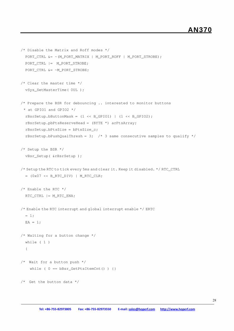
/* Disable the Matrix and Roff modes */
PORT_CTRL &= ~(M_PORT_MATRIX | M_PORT_ROFF | M_PORT_STROBE);
PORT_CTRL |= M_PORT_STROBE;
PORT_CTRL &= ~M_PORT_STROBE; /* Clear the master time */
vSys_SetMasterTime( 0UL ); /* Prepare the BSR for debouncing .. interested to monitor buttons
* at GPIO1 and GPIO2 */
rBsrSetup.bButtonMask = (1 << B_GPIO1) | (1 << B_GPIO2);
rBsrSetup.pbPtsReserveHead = (BYTE *) arPtsArray;
rBsrSetup.bPtsSize = bPtsSize_c;
rBsrSetup.bPushQualThresh = 3; /* 3 same consecutive samples to qualify */ /* Setup the BSR */
vBsr_Setup( &rBsrSetup ); /* Setup the RTC to tick every 5ms and clear it. Keep it disabled. */ RTC_CTRL
= (0x07 << B_RTC_DIV) | M_RTC_CLR; /* Enable the RTC */
RTC_CTRL |= M_RTC_ENA;
/* Enable the RTC interrupt and global interrupt enable */ ERTC
= 1;
EA = 1; /* Waiting for a button change */
while ( 1 )
{ /* Wait for a button push */
while ( 0 == bBsr_GetPtsItemCnt() ) {} /* Get the button data */
28

Tel: +86‐755‐82973805 Fax: +86‐755‐82973550 E‐mail: [email protected] http://www.hoperf.com
A N370
wPtsButton = wBsr_Pop();
} RTC ISR:
/*
*==============================================================================
*
* VISIBLE FUNCTIONS:
*
*/
void vIsr_Rtc
(
void
)
interrupt INTERRUPT_RTC using 1 /* Use RB1 for ISR */
/*------------------------------------------------------------------------------
*
* FUNCTION DESCRIPTION:
* This is the interrupt service routine for RTC.
*
*------------------------------------------------------------------------------
*/
{
/*
*------------------------------------------------------------------------------
*
* VARIABLES:
*
*------------------------------------------------------------------------------
*/ /* Clear the RTL interrupt flag */
RTC_CTRL &= (~M_RTC_INT);
/* Since we are ticking at 5ms, add 5 to the master time to keep
* master time units as [ms] */
vSys_IncMasterTime( 5UL );
29

Tel: +86‐755‐82973805 Fax: +86‐755‐82973550 E‐mail: [email protected] http://www.hoperf.com
A N370
/* Sample the input buttons .. is uses the master time for timestamp */
vBsr_Service();
} /*
*------------------------------------------------------------------------------
*/
30

Tel: +86‐755‐82973805 Fax: +86‐755‐82973550 E‐mail: [email protected] http://www.hoperf.com
A N370
7.2.6. Button Service Module Structures tBsr_Setup
Description: A pointer to a structure of this type is used as an input to the vBsr_Setup() function. The following table lists the members belonging to the tBsr_Setup structure.
Name Type Description
bButtonMask BYTE Mask that specifies which buttons to watch for pushes on: Value 1 in the given bit position means that pushes/ releases are observed and qualified on that GPIO input. See GPIO bit mapping table above. Value 0 means that the associated GPIO input changes are ignored.
pbPtsReserveHead Pointer to BYTE in XDATA
Pointer to head of array of bytes declared by applica-tion to reserve space for the PTS. The array of bytesis actually an array of the tBsr_PtsElement types.
bPtsSize BYTE The depth of the PTS FIFO in button pushes (struc- tures of tBsr_PtsElement type), or the number of qualified button pushes to be stored at any one time.
bPushQualThresh BYTE Number of same consecutive button states needed to qualify a button push/release.
tBsr_PtsElement Description: The PTS is made up of an array of these structures. The following table lists the members belonging to the tBsr_PtsElement structure.
Name Type Description
bButtonVector BYTE Vector of bits representing which button was pushed. 1 .. button was pushed (GPIO connected to the ground) 0 .. button was released See the Button Vector definition above for a mapping of the GPIO to bit number.
bTimestamp BYTE lSys_GetMasterTime() / 32 value which is the time that the button push/release was qualified.
31

Tel: +86‐755‐82973805 Fax: +86‐755‐82973550 E‐mail: [email protected] http://www.hoperf.com
A N370
7.2.7. Button Service Module Functions
vBsr_Setup
Description: Set up the button detection and debouncing for the chip. The function also initializes PTS pointers and attributes, calling the vBsr_InitPts() function internally.
Inputs:
priSetup: (pointer to tBsr_Setup instance) For contents of tBsr_Setup structure see table above.
Outputs:
None
wBsr_Pop
Description: Returns a two byte WORD which contains timestamp information in the MSB byte and the button vector in the LSB byte, effectively returning the tBsr_PtsElement type structure in a WORD variable. The button vector and timestamp represent the oldest qualified button push in the PTS. When there are 0 elements in the PTS this function will return 0. This function also advances the read pointer to the next element in the PTS, removing the currently returned button from information the PTS.
Inputs:
None
Outputs:
Timestamp and button vector: (WORD) MSB byte represent the timestamp bTime- stamp, LSB byte represents is the button vector bButtonVector. Effectively it is a structure of type tBsr_PtsElement packed into the WORD type.
32

Tel: +86‐755‐82973805 Fax: +86‐755‐82973550 E‐mail: [email protected] http://www.hoperf.com
A N370
wBsr_GetCurrentButton
Description: Returns information associated with the latest qualified button push/release. If no pushes have been qualified, it returns 0. The function does not remove the informa- tion from the PTS.
It is the latest information which was pushed at the end of the FIFO if the FIFO was not full before the push. If the FIFO was full then this is the information which would have been pushed, but was dropped, unless it was “no button pressed” change, which gets pushed to the FIFO after it is cleared if the FIFO was full.
The user can use this function to skip over the FIFO content to look ahead what the latest qualified state of the buttons is. The user still needs to check whether the FIFO has any items in it.
Inputs:
None
Outputs:
Button vector and timestamp: (WORD) Upper byte of the word is the timestamp byte. The Lower byte of word is the button vector. Effectively it is a structure of type tBsr_PtsElement packed into the WORD type.
vBsr_InitPts
Description: Initializes the PTS. It initializes the FIFO pointers and clears the contents of the PTS. It is also called from vBsr_Setup() function.
Inputs:
biPtsSize: (BYTE) Number of elements can be stored in the PTS. Each element consists of two bytes, since elements are of the type tBsr_PtsElement.
Outputs:
None
33

Tel: +86‐755‐82973805 Fax: +86‐755‐82973550 E‐mail: [email protected] http://www.hoperf.com
A N370
bBsr_GetPtsItemCnt
Description: Returns the number of items in the PTS. Each item in the PTS FIFO repre- sents a button status change, push or release.
Inputs:
None
Outputs:
PTS item count: (BYTE) The number of elements in the PTS. Each element repre- sents a button push/release.
34

Tel: +86‐755‐82973805 Fax: +86‐755‐82973550 E‐mail: [email protected] http://www.hoperf.com
A N370
vBsr_Service
Description: This function performs the following tasks:
1. Every call of the function samples the input button states. 2. Debounces the button pushes/releases. 3. Writes valid button pushes into the PTS.
It is up to the user application to call this function periodically whenever the input button states need to be sampled.
Inputs:
None
Outputs:
None bBsr_GetTimestamp
Description: Returns lSys_GetMasterTime() / 32 timestamp value.
Inputs:
None
Outputs:
Timestamp: (BYTE) Timestamp value. It is used internally to determine when but- ton push/release occurred, to store it in the PTS.
If application wants to know how long ago that happened, it calls this function to get the current time.
35
Tel: +86‐755‐82973805 Fax: +86‐755‐82973550 E‐mail: [email protected] http://www.hoperf.com
A N370
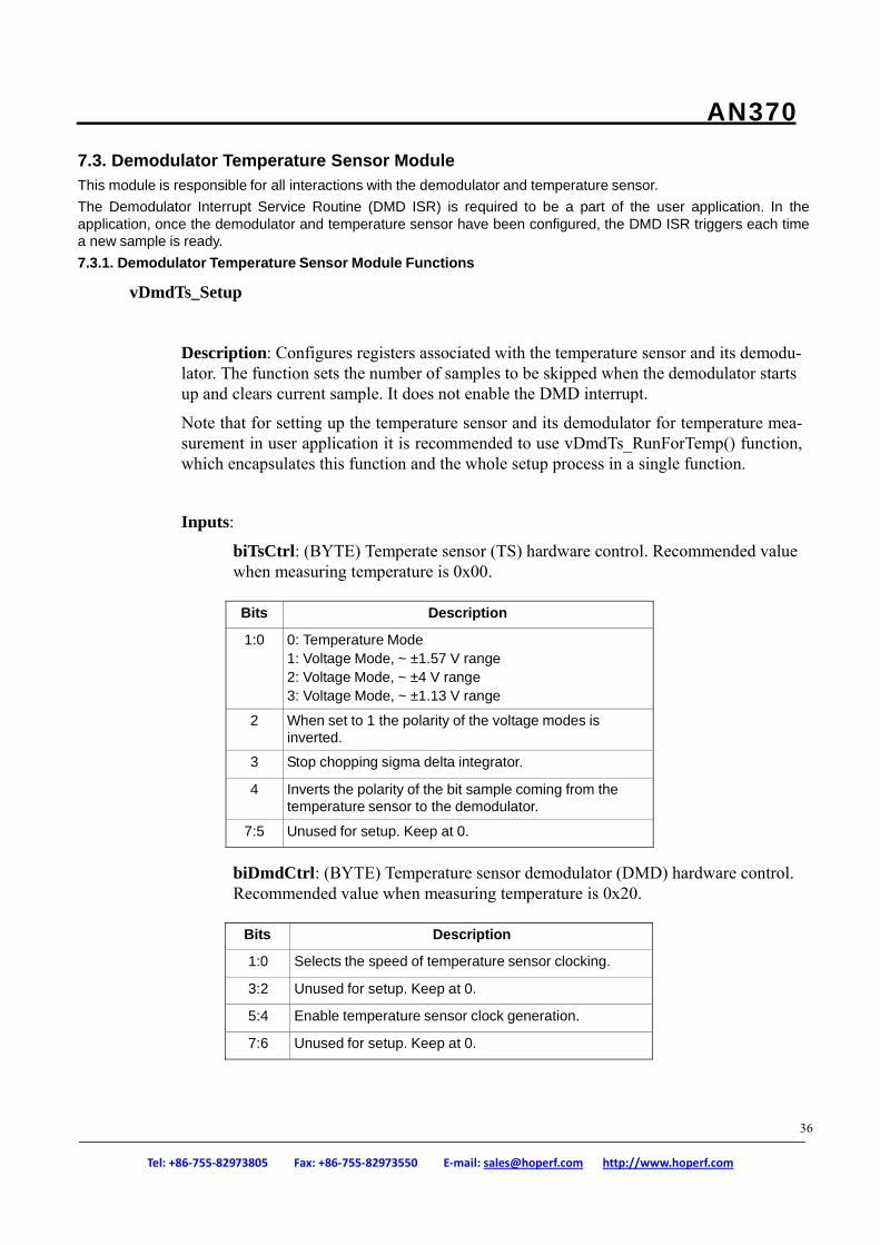
7.3. Demodulator Temperature Sensor Module This module is responsible for all interactions with the demodulator and temperature sensor. The Demodulator Interrupt Service Routine (DMD ISR) is required to be a part of the user application. In the application, once the demodulator and temperature sensor have been configured, the DMD ISR triggers each time a new sample is ready. 7.3.1. Demodulator Temperature Sensor Module Functions
vDmdTs_Setup
Description: Configures registers associated with the temperature sensor and its demodu- lator. The function sets the number of samples to be skipped when the demodulator starts up and clears current sample. It does not enable the DMD interrupt.
Note that for setting up the temperature sensor and its demodulator for temperature mea- surement in user application it is recommended to use vDmdTs_RunForTemp() function, which encapsulates this function and the whole setup process in a single function.
Inputs:
biTsCtrl: (BYTE) Temperate sensor (TS) hardware control. Recommended value when measuring temperature is 0x00.
Bits Description 1:0 0: Temperature Mode
1: Voltage Mode, ~ ±1.57 V range 2: Voltage Mode, ~ ±4 V range 3: Voltage Mode, ~ ±1.13 V range
2 When set to 1 the polarity of the voltage modes is inverted.
3 Stop chopping sigma delta integrator. 4 Inverts the polarity of the bit sample coming from the
temperature sensor to the demodulator. 7:5 Unused for setup. Keep at 0.
biDmdCtrl: (BYTE) Temperature sensor demodulator (DMD) hardware control. Recommended value when measuring temperature is 0x20.
Bits Description 1:0 Selects the speed of temperature sensor clocking. 3:2 Unused for setup. Keep at 0. 5:4 Enable temperature sensor clock generation. 7:6 Unused for setup. Keep at 0.
36

Tel: +86‐755‐82973805 Fax: +86‐755‐82973550 E‐mail: [email protected] http://www.hoperf.com
A N370
biSampleSkipCount: (BYTE) Number of output samples for the function vDmdTs_IsrCall() to skip before collecting values. Upon startup the output of the demodulator is not valid for up to 3 samples. biSampleSkipCount allows for con- figuration of this parameter. Do not use value less then 3.
Outputs:
None iDmdTs_GetData
Description: Returns the current reading of the temperature sensor demodulator.
Inputs:
None
Outputs:
Demodulator Output: (int) Signed output of the demodulator. iDmdTs_GetLatestDmdSample
Description: Returns the latest demodulator reading as recorded by vDmdTs_IsrCall(). It also clears the count of taken samples (sample count) from temperature sensor which is used by application code to determine if a new sample is ready. The sample count can be acquired via the function bDmdTs_GetSamplesTaken().
Upon entry the function records the current value of the EA global interrupt enable bit, disable all interrupts by setting
EA = 0;
Then it does its own processing, and just before return it puts the EA back to the state the function was entered with. The global interrupt disable is very brief (few instructions).
Inputs:
None
37

Tel: +86‐755‐82973805 Fax: +86‐755‐82973550 E‐mail: [email protected] http://www.hoperf.com
A N370
Outputs:
Demodulator Output: (int) Signed output of the demodulator. iDmdTs_GetLatestTemp
Description: Returns the latest temperature demodulator reading converted to tempera- ture. The demodulator reading is the latest reading as recorded by vDmdTs_IsrCall(). This function calls iDmdTs_GetLatestDmdSample(), so it also clears the count of taken sam- ples (see above).
Inputs:
None
Outputs:
Temperature: (int) Signed output representing temperature in internal temperature units, representing temperature as 220 lsb/degC nominal scale with nominal zero point at 25degC. e.g., value 1100 corresponds to 30degC.
vDmdTs_ClearDmd
Description: Clears the temperature sensor demodulator hardware.
Inputs:
None
Outputs:
None vDmdTs_ClearDmdIntFlag
Description: Clears the temperature sensor demodulator interrupt flag.
Inputs:
38

Tel: +86‐755‐82973805 Fax: +86‐755‐82973550 E‐mail: [email protected] http://www.hoperf.com
A N370
None
Outputs:
None vDmdTs_IsrCall
Description: This function is to be called form the user application DMD ISR. It is up to the main application to define a DMD ISR routine. Then this function must be called from within that ISR.
The function skips the number of temperate sensor demodulator samples specified in the biSampleSkipCount argument of the vDmdTs_Setup() function before it produces a new reading. It also updates a samples taken count which can be acquired by the bDmdTs_GetSamplesTaken() function. Once the appropriate number of samples have been skipped then it calls iDmdTs_GetData() and stores the returned value in the local variable. The stored value of the latest sample can be accessed by calling the functions iDmdTs_GetLatestDmdSample() to get the raw sample or iDmdTs_GetLatestTemp() to get the sample converted to temperature in internal units.
Inputs:
None
Outputs:
None bDmdTs_GetSamplesTaken
Description: Returns the number of valid (not skipped!) samples taken by the vDmdTs_IsrCall() since enable or since the number of samples was cleared by reading the latest sample by calling iDmdTs_GetLatestDmdSample() or iDmdTs_GetLatestTemp().
Inputs:
None
Outputs:
39

Tel: +86‐755‐82973805 Fax: +86‐755‐82973550 E‐mail: [email protected] http://www.hoperf.com
A N370
Samples Taken: (BYTE) Number of valid samples taken by the vDmdTs_IsrCall() since enable or last clear of the sample count by reading the latest sample value.
vDmdTs_Enable
Description: Controls the enabling and disabling of the temperature sensor digital demod- ulator (DMD) and the temperature sensor analog block (TS).
Inputs:
biDmdTsSetEnable: (BYTE) Bit 6 enables the digital demodulator (DMD) when set. Bit 7 enables the temperature sensor (TS) analog hardware when set. All other bits are unused. It is recommended to keep them as 0.
Outputs:
None vDmdTs_RunForTemp
Description: Sets up the demodulator and temperature sensor module for running in tem- perature mode. It is a wrapper around the multistep setup procedure to get the TS and DMD running in temperature mode.
This is the recommended function for the user to set up, enable and run the temperature measurement. This function needs to be run only once to enable the TS and DMD.
It calls vDmdTs_Setup() and vDmdTs_Enable() function. It clears and sets up the demod- ulator and temperature sensor from scratch.
The application using this function must include the DMD ISR in order for the application to work properly. Once vDmdTs_RunForTemp() has been run, the user can simply wait for a valid temperature sample and then retrieve it as shown in the following code:
/* Setup the DMD temperature sensor for temperature mode */
vDmdTs_RunForTemp( 3 ); /* Skip first 3 samples */
/* Wait until there is a valid DMD temp sensor sample */
while ( 0 == bDmdTs_GetSamplesTaken() ) {}
/* Retrieve the temperature sample in internal units */
40

Tel: +86‐755‐82973805 Fax: +86‐755‐82973550 E‐mail: [email protected] http://www.hoperf.com
A N370
iCurrentTemp = iDmdTs_GetLatestTemp();
It is important to note that vDmdTs_RunForTemp() forces the DMD interrupt EDMD flag and the global interrupt enable EA flag to be enabled:
EDMD = 1; EA = 1;
Inputs:
biSampleSkipCount: (BYTE) Parameter passed to the vDmdTs_Setup() function. It represents the number of output samples to skip before collecting values in the function vDmdTs_IsrCall(). Upon startup the output of the demodulator is not valid for about 3 samples. biSampleSkipCount allows for configuration of how many samples needs to be skipped. Do not use value less then 3.
Outputs:
None vDmdTs_ResetCounts
Description: Specialized function which resets sample count and initializes the number of samples to skip by vDmdTs_IsrCall() function. Not usually invoked by the user applica- tion and included for possible future extension of the DMD TS API.
The function allows on the fly change of how many samples the vDmdTs_IsrCall() needs to ignore before producing a valid sample.
For example, if the user, for whatever reason, wants to ignore 12 temperature samples before the DMD ISR captures a valid one, the following code could be used:
/* Setup the DMD temperature sensor for temperature mode */
vDmdTs_RunForTemp( 3 ); /* Skip first 3 samples */
/* Wait until there is a valid DMD temp sensor sample */
while ( 0 == bDmdTs_GetSamplesTaken() ) {}
/* Retrieve the temperature sample */
iCurrentTemp = iDmdTs_GetLatestTemp();
41

Tel: +86‐755‐82973805 Fax: +86‐755‐82973550 E‐mail: [email protected] http://www.hoperf.com
A N370
…
/* Skip (ignore) next 12 DMD TS samples */
vDmdTs_ResetCounts( 12 );
/* Wait until there is a valid DMD temp sensor sample */
while ( 0 == bDmdTs_GetSamplesTaken() ) {}
/* Retrieve the temperature sample */
iCurrentTemp = iDmdTs_GetLatestTemp();
42

Tel: +86‐755‐82973805 Fax: +86‐755‐82973550 E‐mail: [email protected] http://www.hoperf.com
A N370
If the user wants to disable the temperature sensor to save power and then restart it later, it is more convenient to disable it and then reconfigure it again from scratch as shown in the following example:
/* Setup the DMD temperature sensor for temperature mode */
vDmdTs_RunForTemp( 3 ); /* Skip first 3 samples */
…
/* Disable the DMD TS interrupt. Make sure that each interrupt
* disable is followed by at least 2 byte instruction! */
EDMD = 0;
EDMD = 0; /* Wasteful, but no need to inspect the assembly */
/* Disable the DMD and TS to save power */
vDmdTs_Enable( 0 );
…
/* Restart the DMD TS for temperature measurement */
vDmdTs_RunForTemp( 3 ); /* Skip first 3 samples */
Inputs:
biSampleSkipCount: (BYTE) number of output samples to skip before collecting values for the function vDmdTs_IsrCall(). This parameter is equivalent to the one passed into vDmdTs_RunForTemp().
Outputs:
None
43

Tel: +86‐755‐82973805 Fax: +86‐755‐82973550 E‐mail: [email protected] http://www.hoperf.com
A N370
7.4. Encoding Module The encoding module provides predefined and customer configurable mechanism for input data conversion for the transmission ready data to be written to the ODS for transmission. There are 3 predefined encodings: none (NRZ), Manchester, and 4 bit to 5 bit encoding. Then users can provide their own functions for custom encoding. The encoding functions in this module are provided to a user as a convenience, but they will not be usually called by the user in the main application. Instead, prior to using the Single Tx Loop module, the user must setup the encoding function by using the vStl_EncodeSetup() function. The selected encoding function is then called from the vStl_EncodeByte() function, which is called from the vStl_SingleTxLoop() function during frame transmission. 7.4.1. No Encoding (NRZ) No encoding means that the input byte is passed “as is” during the encoding process. Note that the bit 0 (LSb) is fed to the PA first in the ODS. To set ODS to shift all 8 bits of the byte to PA the user must set the tOds_Setup.bGroupWidth=7 when calling the vOds_Setup() function. It is also possible that the user prepares the raw data first and requires that, for example, only 6 LSb bits will be transmitted for each byte. In that cast the value tOds_Setup.bGroupWidth=(6-1) has to be used when calling the vOds_Setup() function. 7.4.2. Manchester Encoding Table 6 is used for Manchester encoding. Note that the least significant bit of the output is put onto the PA first. Data bit 0 is encoded to a 1 to 0 transition. Data bit 1 is encoded to a 0 to 1 transition. The least significant bit of the input is converted into two least significant bits of the output. When using this encoding the user is responsible for calling the vOds_Setup() function with the input structure tOds_Setup.bGroupWidth=7 value to transmit all 8 bits in the converted output byte.
Table 6. Manchester Encoding
Input Output 0x0 0x55 0x1 0x56 0x2 0x59 0x3 0x5A 0x4 0x65 0x5 0x66 0x6 0x69 0x7 0x6a 0x8 0x95 0x9 0x96 0xA 0x99 0xB 0x9A 0xC 0xA5 0xD 0xA6 0xE 0xA9 0xF 0xAA
44

Tel: +86‐755‐82973805 Fax: +86‐755‐82973550 E‐mail: [email protected] http://www.hoperf.com
A N370
7.4.3. 4 Bit to 5 Bit Encoding The following table is used for 4 bit to 5 bit encoding. When the last bit of the previously encoded 5 bit value was a 1 the output for the next 5 bit value is an inversion of the output listed below. Keep in mind that the least significant bit of the output is put onto the PA first. When using this encoding the user is responsible for calling the vOds_Setup() function with the input structure tOds_Setup.bGroupWidth=4 value to transmit all 5 bits in the converted output byte.
Table 7. 4 Bit to 5 Bit Encoding
Input Output 0x0 0x15 0x1 0x17 0x2 0x0B 0x3 0x16 0x4 0x0D 0x5 0x1A 0x6 0x1D 0x7 0x12 0x8 0x05 0x9 0x19 0xA 0x0A 0xB 0x1B 0xC 0x09 0xD 0x13 0xE 0x11 0xF 0x0F
The vEnc_4b5bEncode() function uses a global BYTE variable to remember the last bit of the previously encoded 5-bit symbol. It updates the value each time it is called. For the first symbol in a sequence the function vEnc_Set4b5bLastBit() must be called to set this variable for use by initial encoding.
45

Tel: +86‐755‐82973805 Fax: +86‐755‐82973550 E‐mail: [email protected] http://www.hoperf.com
A N370
7.4.4. Custom Encoding The users can provide their own byte encoding. The user will write a custom encoding function and pass a pointer to that function when calling the vStl_EncodeSetup() function. The customer encoding function can encode an input byte to up to 8 bytes of data to be transmitted to the channel if the user is using vStl_SingleTxLoop(). After the custom encoding function is incorporated into the system then the vStl_SingleTxLoop () function will call the custom encoding function with proper pointer to the reserved 8 byte array. The custom conversion function must have the following prototype:
BYTE bEnc_CustomEncode
(
BYTE xdata *pboEncodedBytes, .. ptr to a result byte array
BYTE biByteToEncode .. byte to be encoded
);
Description of the custom encoding function functionality:
bEnc_CustomEncode
Description: The function takes the input byte biByteToEncode and coverts it to an 8 byte array of data (not all 8 output bytes need to be used) to be directly transmitted to the chan- nel by passing the converted bytes directly to the ODS within the vStl_SingleTxLoop().
Not all bits in each byte in the converted array pointed at by pboEncodedBytes pointer need to be used. The ODS serializer takes the encoded byte and starts transmitting pboEn- codedBytes[0] byte, the bit 0 first, followed by bit 1, etc. The bits are therefore transmitted in a little endian fashion.
When using custom encoding the user is responsible for calling the vOds_Setup() function with the input structure tOds_Setup.bGroupWidth value corresponding to the number of LSb bits to be transmitted from each converted output byte minus one. Value 0 corre- sponds with transmitting 1 bit, value 7 corresponds with transmitting all 8 bits.
When calling the vOds_Setup the value of the group width must match the number of valid LSb bits the custom encoding function is actually generating. Making connection in between the encoding function and the encoded group width for the ODS is up to the user in the main application by the vOds_Setup() call.
The custom encoding function is called by the vStl_EncodeByte() which is called from vStl_SingleTxLoop() function.
representing temperature as 220 lsb/degC nominal scale with nominal zero point at 25degC. E.g. value 1100 corresponds to 30degC.:
pboEncodedBytes: (pointer to BYTE in XDATA) Pointer to the head of the 8 byte array which will contain the resulting encoded bytes. The value of the pointer will be provided at runtime by the vStl_EncodeByte() function and the array is reserved in the API reserved XDATA area.
46

Tel: +86‐755‐82973805 Fax: +86‐755‐82973550 E‐mail: [email protected] http://www.hoperf.com
A N370
biByteToEncode: (BYTE) Input byte to be encoded
Outputs:
pboEncodedBytes: (pointer to BYTE in XDATA) Up to 8 valid encoded bytes in output array.
Valid encoded array size: (BYTE): Number of bytes in the output array pboEn- codedBytes which are valid after encoding. Valid values are 1 through 8. Any other return value will result in system instability.
One example for the custom encoding function might be the uncoded transmission using big endian rather then little endian. The ODS shifts bits from a byte with b0 going to the PA first. If the user wants bit 7 to go first instead, there are two options: 1. Bit flip all the data before transmission and set bEnc_NoneNrz_c no encoding. 2. Write a bit reverse function as a byte encoding custom function and use bEnc_Custom_c custom encoding.
The input data to the transmission chain will be unchanged and the bit flipping will happen just before the byte is to be transmitted.
Users might find the latter approach more convenient. 7.4.5. Encoding Module Functions
vEnc_4b5bEncode
Description: The function 4b5b encodes a byte into two bytes. Each byte contains the 5 bit encoded result of the corresponding nibble from the input byte. The bits are encoded in the little endian fashion.
Prior to calling this function for the first time per transmitted frame the vEnc_Set4b5bLastBit() must be called to set the initial value of the last bit that the 4b5b encoding references. The last bit of the previous encoded value affects the encoding of the next encoded value by inverting its bits when the last bit was a 1. The vEnc_4b5bEncode() function updates the last bit.
That means that when using 4b5b encoding the user must call the vEnc_Set4b5bLastBit() prior to calling the vStl_SingleTxLoop() every time.
Inputs:
pboEncodedBytes: (pointer to xdata BYTE ) Pointer to the head of the 2 byte array which will contain the resulting encoded bytes. The caller must declare this array.
biByteToEncode: (BYTE) Byte to be encoded.
Outputs:
pboEncodedBytes: (pointer to BYTE in XDATA) Updated 2 byte array with resulting encoded bytes.
Valid encoded array size: (BYTE): Number of bytes in the output array pboEn- codedBytes which are valid after conversion. In this case the value is 2.
47

Tel: +86‐755‐82973805 Fax: +86‐755‐82973550 E‐mail: [email protected] http://www.hoperf.com
A N370
vEnc_Set4b5bLastBit
Description: Sets the initial value of the bit that the 4b5b encoding references as the last bit of the previously encoded group of 5. The encoding of each group depends on the last bit of the previously encoded group. This function must be called before each frame trans- mission when using the 4b5b encoding.
Inputs:
bLastBitValue: (BYTE) The least significant bit in this byte is used to initialize the last bit of the previously encoded group variable.
Outputs:
None bEnc_ManchesterEncode
Description: Manchester encoding of the input byte. Each input byte is converted into two bytes. One bit, after being Manchester encoded, results in two bits. Note that the bit 0 of the input byte is converted to the bits 0 and 1 of the pboEncodeByte[0] byte. The bit 7 of the input byte is converted to the bits 6 and 7 of the pboEncodeByte[1].
The bits are therefore converted in the little endian fashion. The ODS will process the pbo- EncodedByte array such that the bit 0 of the byte pboEncodeByte[0] will get transmitted first, etc.
Inputs:
pboEncodedBytes: (pointer to BYTE in XDATA) Pointer to the head of the two byte array which will contain the resulting encoded bytes. The caller must declare this array.
biByteToEncode: (BYTE) Byte to be encoded.
Outputs:
pboEncodedBytes: (pointer to BYTE in XDATA) Updated 2 byte array with resulting encoded bytes.
Valid encoded array size: (BYTE): Number of bytes in the output array pboEn- codedBytes which are valid after conversion. In this case the value is 2.
48

Tel: +86‐755‐82973805 Fax: +86‐755‐82973550 E‐mail: [email protected] http://www.hoperf.com
A N370
7.5. Frequency Counter Module This module is responsible for interfacing to the frequency counter (FC). 7.5.1. Frequency Counter Key Terms Table 8 lists key terms used in describing the Frequency Counter (FC) module.
Table 8. Frequency Counter Terms
Term Definition
Counter mode Determined by the source for the interval clock.
Interval Number of interval clock cycles during which divider clock cycles are counted.
Divider clock Input clock which is counted during the specified interval.
7.5.2. Frequency Counter Module Functions
vFc_Setup
Description: Sets up the counter mode, divider selector and number of clock cycles in an interval. It clears any previous frequency counter settings.
Inputs:
biFcCtrl: (BYTE) Select the counter mode and divider selector. The counter mode is essentially the interval clock source. The table describes the purpose of each bit in this input parameter.
Bits Purpose
2:0 Counter Mode. 0: Off 1: Reference clock from GPIO3 2: Undivided LPOSC (24 MHz) 3: Divided LPOSC (system clock) 4: Crystal oscillator from GPIO0 5: Reserved 6: Sleep timer output 7: GPIO output pulse
5 Divider Clock. Which clock is being counted during the interval: 0: LC Oscillator 1: Divider
49

Tel: +86‐755‐82973805 Fax: +86‐755‐82973550 E‐mail: [email protected] http://www.hoperf.com
A N370
Remaining bits are unused and can have any value. Value 0 is recommended.
biFcInterval: (BYTE) Controls the number of interval clock cycles during which the divider clock cycles are counted. The biFcInterval value is not the actual num- ber of interval clock cycles used. The actual number of interval clock cycles is cal- culated by the following equation:
Ninterval_cycles = (2 + biFcInterval[0]) * 2biFcInterval[5:1]
Example: An argument of 17 = 0x11 yields the following:
Outputs:
Ninterval_cycles = (2 + 1) * 28 = 768
None vFc_StartCount
Description: Starts the frequency counter.
Inputs:
None
Outputs:
None vFc_PollDone
Description: Polls the frequency counter busy flag and waits until the counter is done. To be called after starting the frequency counter. Note that if something happens in hardware (loss of the interval clock, for example), and the frequency counter stalls and does not fin- ish counting, this function will wait for frequency counter to be done indefinitely in an infinite loop. There is no timeout incorporated in the loop. It is up to the user to setup an interrupt driven timer as a watchdog if the timeout is desired.
Inputs:
None
50

Tel: +86‐755‐82973805 Fax: +86‐755‐82973550 E‐mail: [email protected] http://www.hoperf.com
A N370
Outputs:
None lFc_GetCount
Description: Returns the latest value of the frequency counter. To ensure a correct reading vFc_PollDone() should be called prior to a call to this function. This function can be called any time to get the “on the fly” reading of the frequency counter.
Inputs:
None
Outputs:
Frequency Count: (LWORD): Current frequency count. lFc_StartPollGetCount
Description: A combination of vFc_StartCount(), vFc_PollDone() and lFc_GetCount(). After calling vFc_Setup() this function can be called and will return the current frequency count after the counter stopped counting.
Inputs:
None
Outputs:
Frequency Count: (LWORD): Final frequency count.
51

Tel: +86‐755‐82973805 Fax: +86‐755‐82973550 E‐mail: [email protected] http://www.hoperf.com
A N370
7.6. Frequency Casting Module This module is responsible for adjusting the output frequency to the desired value before transmission and setting up parameters which allow for temperature compensation during transmission inside the Single Tx Loop (see Stl module). It is also responsible for optional output frequency calibration using crystal oscillator. 7.6.1. Frequency Casting Module Structure Types
tFCast_XoSetup
Description: A pointer to a structure of this type is used as an input to the vFCast_XoSetup() function. The following table lists the members belonging to the tFCast_XoSetup structure.
Name Type Description
fXoFreq float Frequency of the external oscillator in [Hz].
bLowCap BYTE Controls the XO_LOWCAP register bit. If 0x00 value then the bit is set to 0, if other then 0x00 value then the bit is set to 1.
7.6.2. Frequency Casting Module Functions
vFCast_Setup
Description: Frequency casting initialization. This function should only be called only once per boot. It is to be called prior to any calls to vFCast_Tune(). Once called the fre- quency casting is initialized for use.
Inputs:
None
Outputs:
None
vFCast_XoSetup
Description: Crystal oscillator (XO) setup and enable. The functions sets the XO parame- ters based on the passed values in the tFCast_XoSetup structure instance. Then it turns the XO on by setting the XO enable bit (mask M_XO_ENA) in the bXO_CTRL register.
Frequency casting function vFCast_Tune() will look at the bXO_CTRL.XO_ENA bit and if the bit is set then it will use the crystal oscillator, otherwise it will use its own internal algorithm for frequency calibration.
52

Tel: +86‐755‐82973805 Fax: +86‐755‐82973550 E‐mail: [email protected] http://www.hoperf.com
A N370
The user can turn the XO on and off as required by, for example, using the following C code:
bXO_CTRL &= (~M_XO_ENA); /* Turning the XO off */
…
bXO_CTRL |= M_XO_ENA; /* Turning the XO on */
Inputs:
priXoSetup: (pointer to tFCast_XoSetup instance) XO setup data. See the tFCast_XoSetup table above.
Outputs:
None vFCast_Tune
Description: Tunes the device’s output frequency to the desired frequency. The input fre- quency is provided as a float 32-bit number and is in [Hz].
The function also calculates necessary data to be used by the single Tx loop main function, vStl_SingleTxLoop(), for fine frequency correction during transmission.
The user can call this function in between packets, or just once before transmission. It takes about ~5ms to execute this function. The function forces internal clock to run at fast- est rate, 24MHz. The original clock rate is restored before exiting.
The frequency calculation is controlled by the fact whether the crystal oscillator is enabled or not. The function checks the value of the bXO_CTRL.XO_ENA bit. If the XO is enabled, it is used for frequency tuning. If the XO is disabled an alternative internal algo- rithm is used.
As with vDmdTs_RunForTemp() this function forces on the DMD interrupt enable and the global interrupt enable.
EDMD = 1; EA = 1;
The vFCast_Tune() function calls the DMD clear, setup, and run function vDmdTs_RunForTemp(). Therefore, after vFCast_Tune() completes, the user can retrieve the temperature readings as shown in the vDmdTs_RunForTemp() description above. There is no need for any further DMD setup – the vFCast_Tune() function does it.
53
Tel: +86‐755‐82973805 Fax: +86‐755‐82973550 E‐mail: [email protected] http://www.hoperf.com
A N370
The function also forces the LC oscillator on and leaves it turned on, since this function should be followed by a call to vPa_Tune() for antenna tuning where the LC oscillator running is required. Since it takes about 125us for LC to stabilize, the vFCast_Tune() leaves the LC on to save time. The vPa_Tune() turns the LC off. If the user desires to turn the LC off, the following code can be used:
ODS_CTRL &= (~M_FORCE_LC);
This will turn off the LC force on bit.
Inputs:
fiDesiredFreq: (float) Desired output frequency in [Hz].
Outputs:
None vFCast_FineTune
Description: Fine tunes the LC oscillator frequency based on the temperature reading pro- vide as input. It is called from within the vStl_SingleTxLoop() function during the frame transmission.
The typical usage in the customer code if not using the provided vStl_SingleTxLoop() function would be to do the following in a transmission loop:
/* Check if valid temperature sample is ready */
if ( 0 < bDmdTs_GetSamplesTaken() )
{
/* Calculate the LCOSC fine tune value and apply it. */
vFCast_FineTune( iDmdTs_GetLatestTemp() );
}
Inputs:
iiCurrentTemp: (int) Signed output representing temperature in internal tempera- ture units 220 bits/degC. It is the output of the iDmdTs_GetLatestTemp() function.
54

Tel: +86‐755‐82973805 Fax: +86‐755‐82973550 E‐mail: [email protected] http://www.hoperf.com
A N370
Outputs:
None vFCast_FskAdj
Description: Takes the desired FSK deviation and adjusts the actual FSK deviation needed based on the results of frequency casting. It is to be called after each call to vFCast_Tune(). The input to this function is attained by using the RF60 calculation spreadsheet, RF60_calc_regs.xls. It should be an application parameter.
Inputs:
biFskDev: (BYTE) Desired FSK deviation number based on the supplied spread- sheet calculation.
Outputs:
None
55

Tel: +86‐755‐82973805 Fax: +86‐755‐82973550 E‐mail: [email protected] http://www.hoperf.com
A N370
7.7. HVRAM Module The HVRAM module interfaces to the HVRAM. HVRAM in the RF60 consists of 64 bits (8 bytes) of battery backed RAM. As long as the power is connected to the chip the HVRAM keeps its content. The content of the HVRAM is not affected by shutting down the chip by vSys_Shutdown() function. 7.7.1. HVRAM Map Table 9 lists the HVRAM fields that have been reserved for the API use in RKE application.
Table 9. HVRAM Fields
Field Byte Addr
Bits Description
Improper shutdown 0 0 This bit is used to determine when the chip did not shut- down properly. Upon boot, if this bit is a 1, it wasn’t cleared in the previous shutdown of the chip, and special action needs to be taken.
Bad shutdown count 1 7:0 Count of bad shutdowns. Battery voltage 2 7:0 Latest measured battery voltage.
7.7.2. HVRAM Module Functions
vHvram_Write
Description: Writes data byte to the specified HVRAM address.
Inputs:
biWriteAddr: (BYTE) HVRAM address to write to. Only bottom 3 bits are used, the rest is ignored.
biWriteData: (BYTE) Byte to be written.
Outputs:
None
cbHvram_Read
Description: Reads data byte from the specified HVRAM address.
Inputs:
biReadAddr: (BYTE) HVRAM address to read from. Only bottom 3 bits are used, the rest is ignored.
Outputs:
Read Data: (BYTE) Data that resulted from the HVRAM read.
56
Tel: +86‐755‐82973805 Fax: +86‐755‐82973550 E‐mail: [email protected] http://www.hoperf.com
A N370
7.8. Multi Time Programmable (MTP) Memory Module The multi-time programmable (MTP) memory (EEPROM) module functions deal with four 20-32 bit counters stored in the MTP non-volatile memory. In general the functions associated with the MTP module read and increment counters stored in the MTP memory. Actual counter values stored in the MTP are in special encoded format, not in the counter decimal representation. Users may change the contents of the memory at their own risk. The supplied API functions expect the contents of the MTP to be in balanced gray encoded format. The purpose for balanced gray encoding is to limit the number of transitions on any single bit of the memory. The user is free to use any part of the MTP memory for different purposes. The memory is accessed as 128 bit 1 serial one bit in/128 bit parallel bits out. If the user wants to change a single bit in the MTP then all 128 bits need to be read, single bit changed, and all 128 bits have to be put back into the MTP. There is no bit addressing in the MTP. 7.8.1. MTP Memory Module Global Variables The parallel 128 bit output of the MTP is organized into the read only 16 byte array
abMTP_RDATA[16]
Read only array of 16 bytes where the contents of the MTP can be read upon strobing of the MTP outputs by vMtp_Strobe() function. This array is a read only array mapped into the XDATA space.
This array is updated from MTP when the vMtp_Strobe() function is called. The functions pbMtp_Read() and bMtp_Write() call the vMtp_Strobe() before return, so after calling those two functions the array contains the MTP content.
7.8.2. Working with MTP The user can choose not to use the balanced counters as implemented by API. The user is free to work with any bit in the MTP memory. Given the asymmetric nature of the MTP there are rules the user should follow to work with MTP raw data: 1. Any bit in the MTP can change state only up to 50,000 times. Since during programming all the bits which are
not being changed have to be put back into the MTP in their read state, it is worth noting that the fact that some bits are changing values is not counted against the longevity of the bits for which the value is not changed.
2. The user must copy the read only array abMTP_RDATA[16] to XDATA RAM memory by calling pbMtp_Read() function. The function returns a pointer to the 16 byte array in XDATA where the read only array abMTP_RDATA[16] was copied to. The XDATA RAM array is part of the API reserved area. Note that every call to pbMtp_Read() will return the same pointer value – the XDATA location of the mirror array is fixed.
3. All the desired changes must be done on the XDATA array, pointer to which was returned by abMtp_Read()
data. 4. Call the bMtp_Write() function to write the modified data from XDATA array to MTP. It is up to the application responsibility not to stress any of the MTP bits over the specified limit. 7.8.3. Working with Balanced Counters This module implements API functions which implement balanced counters (counting up), such that the application can use an MTP based counter which counts up to 1.040 million counts while no stressing any of the MTP bits over the 50,000 cycle limit. The counter width in this section means overall balance counter width in bits, which are needed to store the counter value in MTP. The module supports up to 4 to 5 counters with the following independent configurations per counter.
57

Tel: +86‐755‐82973805 Fax: +86‐755‐82973550 E‐mail: [email protected] http://www.hoperf.com
A N370
Counter Width MTP Bytes Max Value biNibbleCnt
20 bits 3 550k 3
24 bits 3 730k 4
28 bits 4 915k 5
32 bits 4 1040k 6
If the user is using only 20 or 24-bit counters which require only 3 bytes of MTP storage then it is possible to have 5 such counters in the system with one byte to spare for independent user usage. It is not possible to decrement any of the counters, but it is possible to initialize the counter with a customer chosen value at any time. The counters are manipulated in XDATA RAM, so the following flow must be followed when updating any counter value(s): 1. Copy the read only array abMTP_RDATA[16] to XDATA RAM memory by calling pbMtp_Read() function. The
function returns a pointer to the 16 byte array in XDATA, which is known to all the counter manipulation functions. Therefore, if working with balanced counters only, the return value of the pbMtp_Read() function can be ignored.
2. Manipulate the selected counter or counters by vMtp_SetDecCount(), lMtp_GetDecCount(), and/or vMtp_IncCount(). Those functions take biIndex indicating the starting byte index of the counter in the 16-byte array and the biNibbleCnt to determine the counter width. Note that the biNibbleCnt has different meaning then how much bytes each counter occupies in the MTP. See the table above.
3. Call the bMtp_Write() function to write the modified counter data to MPT. It is up to the application to determine at what 16-byte array index, value 0 to 15, each counter begins. The only requirement is that the counter bytes in the MTP must not overlap. The value of the byte index, biIndex, is then passed to all the functions manipulating the particular counter. It is recommended, but not required, that the index values are 0, 4, 8, and 12 for uniformly spaced counters in the MTP. 7.8.4. MTP Write Function and Interrupts Very important: The main MTP programming function bMtp_Write() is time sensitive. In general, the MTP programming process will produce unpredictable results if interrupted, even possibly damaging the MTP memory. The function stores the original EA bit value upon entry and disables all the interrupts by setting EA = 0 around critical parts of the code. Since the programming of the MTP takes about 9 ms, and can go up to 40 ms in some cases, for some application having interrupts completely disabled during that period might be too disruptive. The user can specify the maximum programming time after which, if the MTP programming is not finished, the bMtp_Write() function will return with an error. To allow for some critical interrupts to be serviced when executing the bMtp_Write() function, the global interrupts are disabled only during critical parts of the MTP timing generation within bMtp_Write(). Therefore, for all practical purposes, the global interrupts are enabled within the bMtp_Write() function. If the interrupts are enabled when calling bMtp_Write() function it is the responsibility of the user application that in every 1 ms sliding time window the compound time spent in all ISR routines is less then 120 µs. Be advised that when the interrupt is invoked from within the bMtp_Write() function the device internal system clock might be forcibly running at 24 MHz. If in any 1ms sliding time window the ISR interrupt time is more then 120 µs the MTP proper functionality is no longer guaranteed and MTP hardware damage may occur. It is highly recommended, if at all possible, that the interrupts are disabled by EA = 0 in the user application before calling the bMtp_Write() function and enabled afterwards to avoid any problems, if at all possible. If not possible then at least keep only critical interrupts, which really have to be serviced urgently, enabled during the bMtp_Write() call and make the ISR for those really short.
58

Tel: +86‐755‐82973805 Fax: +86‐755‐82973550 E‐mail: [email protected] http://www.hoperf.com
A N370
7.8.5. MTP Module Functions
lMtp_GetDecCount
Description: Given the starting index of a counter in XDATA array this function returns the decoded content of the balanced counter as a 32-bit unsigned value.
The user must call the pbMtp_Read() first before working with this function.
Inputs:
biIndex: (BYTE) Starting byte index of the counter in the MTP array. Recom- mended values: 0, 4, 8, 12.
biNibbleCnt: (BYTE) Width of the counter (see biNibbleCnt table above.) Valid values: 3 through 6.
Outputs:
Counter value: (LWORD) Decoded value of the counter stored at the specified index.
vMtp_IncCount
Description: Increments, by one, the value of the counter starting at the specified byte index in the MTP. The user must call the pbMtp_Read() first before working with this function.
This function does not write the incremented value into the actual MTP. In order to write the incremented value into the MTP memory the user should call the bMtp_Write() func- tion.
Inputs:
biIndex: (BYTE) Starting byte index of the desired counter in the MTP array. Rec- ommended values: 0, 4, 8, 12.
biNibbleCnt: (BYTE) Width of the counter (see biNibbleCnt table above.) Valid values: 3 through 6.
59

Tel: +86‐755‐82973805 Fax: +86‐755‐82973550 E‐mail: [email protected] http://www.hoperf.com
A N370
Outputs:
None vMtp_SetDecCount
Description: Converts an input decimal value to the internal counter representation for- mat used in the MTP. This function allows user to load predefined decimal value to the counter. The user must call the pbMtp_Read() first before working with this function.
This function does not write the updated counter value into the actual MTP. In order to write the updated counter value into MTP memory the user should call the vMtp_Write() function.
Inputs:
pliDecValue: (Pointer to LWORD in XDATA) Pointer to a new desired value of the counter. Needed to be done through a pointer since it is not possible to pass LWORD value and additional parameters to the function in registers only.
biIndex: (BYTE) Starting byte index of the desired counter in the MTP array. Rec- ommended values: 0, 4, 8, 12.
biNibbleCnt: (BYTE) Width of the counter (see biNibbleCnt table above.) Valid values: 3 through 6.
Outputs:
None bMtp_Write
Description: The function writes all 128 bits of the global XDATA RAM array into the MTP. It is highly recommended that all interrupts be disabled before calling this function. This is because the write operation to the MTP is time sensitive and interrupts could cause an unpredictable result during write. See the complete discussion about interrupts during the bMtp_Write() execution above.
The function applies programming cycles until the MTP memory returns a status that all bits were updated successfully. There is no predefined number of cycles. Each program- ming cycle takes about 1 ms. It typically takes about 9 ms to update the MTP content.
60

Tel: +86‐755‐82973805 Fax: +86‐755‐82973550 E‐mail: [email protected] http://www.hoperf.com
A N370
However, the MTP module is rated to finish programming within 40 ms. For some appli- cations having a possible randomness in the time spent in this function might not be desir- able.
Therefore, the user can limit the maximum number of cycles of the MTP programming. If the MTP is not programmed correctly after the user defined number of the cycles, the function returns an error. Otherwise, the function returns as soon as the MTP hardware reports that all the bits were programmed correctly.
When using the IDE for debugging it is required that the user uses the Step Over (F10) toolbar button and neither the Step (F11) nor Multiple Step toolbar but- tons when stepping over this function.
Inputs:
biProgLimit: (BYTE) Maximum number of MTP programming cycles allowed by the user. The recommended value is 40. The user should not use value bigger then 50 or smaller then 15..
Outputs:
Status: (BYTE) MTP programming status: 0 .. Success: MTP programmed correctly 1 .. Error: Maximum user specified number of MTP programming cycles reached before MTP reported that all bits were programmed cor- rectly.
vMtp_Strobe
Description: This function strobes the MTP to read the contents from into the XDATA mapped read only array abMTP_RDATA[16]. This function is automatically called by pbMtp_Read() and bMtp_Write() functions just before returning from them.
The function stores the global EA interrupt enable flag at the beginning, disables all the interrupts during the function execution, and restores the EA value just before returning from the function.
The function stores the current SYSGEN_DIV field of SYSGEN SFR and forces it to 0, forcing the fastest, 24 MHz, system clock frequency. Before returning, the function restores the SYSGEN_DIV to its original value.
The function execution time is about 4µs.
61

Tel: +86‐755‐82973805 Fax: +86‐755‐82973550 E‐mail: [email protected] http://www.hoperf.com
A N370
Inputs:
None Outputs:
None pbMtp_Read
Description: Copy 128 bits out of the XDATA read only MTP output array abMTP_RDATA[16] into the global 16-byte XDATA RAM array. The function returns a pointer to XDATA to the head of the internal RAM array. This function calls the vMtp_Strobe() function to latch the internal MTP content to its output registers.
All functions working with the balanced counters as well as the abMtp_Write() function works on this internal XDATA RAM array.
Inputs:
None
Outputs:
MTP RAM byte array pointer: (pointer to BYTE in XDATA) Pointer to a byte array in XDATA where the abMTP_RDATA[16] got copied to.
62

Tel: +86‐755‐82973805 Fax: +86‐755‐82973550 E‐mail: [email protected] http://www.hoperf.com
A N370
7.9. Battery Voltage Measurement Module This module measures unloaded and loaded battery voltage. 7.9.1. Battery Measurement Module Functions
iMVdd_Measure
Description: Measures the battery voltage. It can be used in one of two modes.
1. If biWait == 0 then it measures the battery voltage when the battery is loaded with current user application.
2. If biWait > 0 it measures battery voltage of forcibly loaded battery, where loading is achieved by temporarily turning on major power hungry parts of the device.
The function requires that the temperature sensor demodulator DMD ISR interrupt service routine is present in the user application.
The function does the following tasks in order:
1. Configure the DMD TS hardware for voltage mode measurement.
2. Forcibly enable DMD interrupt, EDMD = 1
3. Temporarily force overall global interrupt enable EA = 1. It remembers the state of the EA bit as it was upon entering the function.
4. Measure the unloaded battery voltage.
5. Only if biWait > 0 make a loaded battery measurement:
6. Remember the current system clock speed and switch the system clock to slower pace.
7. Remember the current state of PA, DIV divider, and LC oscillator.
8. Forcibly enable PA, DIV, and LC oscillator. Note that even though the PA is enabled, there is no RF power radiated to the antenna. The PA is configured such that it loads the battery the same way as if it is driving an antenna.
9. Wait for biWait x 17 µs
10. Measure the loaded battery voltage using the DMD ISR interaction.
11. Restore the original PA, divider, and LC state.
12. Restore the original system clock frequency.
13. Forcibly disable DMD interrupt, EDMD = 0.
14. Restore the original value of the global EA bit.
15. Return the battery voltage measurement converted to [mV].
The function should be called on its own outside of the transmission since it has a signifi- cant system impact. The user is advised to reinitialize the affected blocks after calling this function.
63
Tel: +86‐755‐82973805 Fax: +86‐755‐82973550 E‐mail: [email protected] http://www.hoperf.com
A N370
The temperature sensor demodulator DMD interrupt will be forcibly disabled at the end of the measurement:
EDMD = 0;
The user needs to take this into account.
When using the IDE for debugging it is required that the user uses the Step Over (F10) toolbar button and neither the Step (F11) nor Multiple Step toolbar but- tons when stepping over this function.
Inputs:
biWait: (BYTE) Wait in 17 µs increments in between the enabling of the heavy load blocks on the device and before the battery measurement is taken. If the value is 0, then the battery measurement is taken immediately with the current load of the chip. If the value is not 0, the chip is loaded by enabling the PA, DIV divider, and LC oscillator. The function then waits for (biWait x 17 µs) before the battery measurement is taken.
Outputs:
Measured voltage: (int) Measured battery voltage in [mV].
64
Tel: +86‐755‐82973805 Fax: +86‐755‐82973550 E‐mail: [email protected] http://www.hoperf.com
A N370
7.10. Non-Volatile Memory (NVM) Copy Module The non-volatile memory (NVM) module copies formatted (composed) code and data blocks from the NVM. The data within NVM block can be copied to CODE/XDATA RAM, as well as to the internal DATA/IDATA RAM. The sole purpose of this module is for the user to load user application code and data overlays from NVM by the application at runtime. If using overlays, the user application consists of the main program (User Boot), which is loaded to the CODE/ XDATA RAM upon boot and run. The application can be written to be able to load then new or additional code and/ or data from NVM in a form of an overlay. That mechanism will allow the use of the 7 kB of NVM available code/ data for user application, while having only 4 kB of RAM where the code can be run from. The data will be programmed into the NVM by a special application. Application note will be issued how to program the NVM. The NVM handling is split into several functions. Usually the overlay will consist of a single IntelHEX compiled and linked output file, which will be converted to a single NVM block. In the case of loading an overlay consisting of one NVM block, the user needs to enter only the overlay starting address where the converted overlay resides in the NVM. Below is an example of a wrapper function which enables the NVM, copies a single NVM block, and disables the NVM to conserve power. The setting up of the NVM by vNvm_McEnableRead() can take up to 30 µs. It usually takes 3.6 ms per 1 kB of NVM data to be copied from NVM by bNvm_CopyBlock() function. Important note about interrupts: It is highly recommended that interrupts be disabled around the call to the bNvm_CopyBlock() and bNvmLoadBlock() functions. If this is not possible, then it is highly recommended that the most time consuming interrupts are disabled. The interrupt disruption of the NVM load process should be kept at a minimum in the order of units of microseconds. In general, the interrupts should be disabled before the vNvm_McEnableRead() call and enabled only after the vNvm_McDisableRead() call. There should be no other activity in between these two functions when the NVM module function calls as shown in the bNvmLoadBlock() function example below.
/*
*------------------------------------------------------------------------------
*
* INCLUDES:
*/
#include "RF60.h"
#include "RF60_api_rom.h" /*
*==============================================================================
*
* VISIBLE FUNCTIONS:
*/
BYTE vNvmLoadBlock
( WORDwiNvmAd
dr
)
/*-------------------------------------------------------------
65

Tel: +86‐755‐82973805 Fax: +86‐755‐82973550 E‐mail: [email protected] http://www.hoperf.com
A N370
*
* FUNCTION DESCRIPTION:
* Load one overlay block from NVM.
*
*-------------------------------------------------------------
*/
{
/*
*-------------------------------------------------------------
*
* VARIABLES:
*/
BYTEbStatus; /* Return bNvm_CopyBlock status */ /*
*-------------------------------------------------------------
*/
vNvm_McEnableRead(); /* Enable analog hardware and NVM for read */
vNvm_SetAddr( wiNvmAddr ); /* Set the NVM block first address */
bStatus = bNvm_CopyBlock(); /* Copy the NVM block from NVM */
vNvm_McDisableRead(); /* Disable analog hardware and NVM */
/* Return bNvm_CopyBlock status */
return ( bStatus );
} /*
*------------------------------------------------------------------------------
*/
It is up to the user to include the function above into the application. It is not part of API in ROM.
66

Tel: +86‐755‐82973805 Fax: +86‐755‐82973550 E‐mail: [email protected] http://www.hoperf.com
A N370
7.10.1. Non-Volatile Memory Copy Module Functions
vNvm_SetAddr
Description: Sets the NVM address where the next invocation of bNvm_CopyBlock() will start copying from NVM. The NVM composer and burner will correctly format the user input IntelHEX files into the NVM block data structures required by this function.
The NVM occupies addresses 0xE000 to 0xFFFF. The NVM address must lie in this range. Not all NVM is available to the user. The user should not use address which is less than the content of the wBoot_NvmUserBeg variable after boot. The last 64 bytes of the NVM, at addresses from 0xFFC0 to 0xFFFF.
Those last 64 bytes of the NVM will not be copied by the vNvm_CopyBlock() function.
Inputs:
wiAddr: (WORD) The 16 bit NVM start address of the NVM block to be copied by the next call to the bNvm_CopyBlock.
Outputs:
None
wNvm_GetAddr
Description: Returns the NVM address from which the next call to the bNvm_CopyBlock() is going to start copying the NVM data.
This address is set either by the vNvm_SetAddr(). It is also updated by the bNvm_CopyBlock() call. If the user calls this function immediately after the bNvm_CopyBlock() then return value is the first NVM unread address after the last NVM read address by the bNvm_CopyBlock() function. The user then can use this information to determine whether the block was copied in its entirety. This can be useful for checking whether an overlay was read correctly from the NVM since the user would know in advance what the NVM address range of the particular overlay block is in the NVM.
Inputs:
None
Outputs:
Start NVM address: (WORD) NVM address where the next bNvm_CopyBlock() call going to start in NVM.
67

Tel: +86‐755‐82973805 Fax: +86‐755‐82973550 E‐mail: [email protected] http://www.hoperf.com
A N370
bNvm_CopyBlock
Description: Copy a single NVM block of composed data from NVM. Based on the data destination address found in the NVM block this function can copy data to CODE/ XDATA 4.5KB RAM, as well as to the DATA/IDATA internal RAM region.
Therefore, the user can use the NVM blocks to initialize the variables to desired initial val- ues by loading them from the NVM.
The function starts copying from NVM address specified by vNvm_SetAddr() call or by a previous call to bNvm_CopyBlock() for back to back blocks in NVM.
If an error is encountered while copying NVM data, value of 0xFF is returned. This can happen in three possible scenarios:
1. The first byte of the NVM block was not a valid block start flag (0xFF). 2. During a copy process the NVM address entered invalid NVM region. That hap-
pens when the NVM address reaches the last 64 bytes of NVM, which are reserved for factory use.
3. Special return jump inside the NVM block was used, but the next NVM address was outside the valid NVM address space. This is an advanced feature supported by special application note and not used by majority of users.
If no error is encountered, and the copy finishes successfully, the function returns an NVM block return value byte found after the block end flag. For the User Application (overlay) block in NVM the user NVM block return value is fixed to 1 when using the NVM composer/programmer. The NVM block return value can be changed by advanced NVM manipulation but there is no reason to do that for majority of users.
It is highly recommended that the NVM copy process is not interrupted and the interrupts to be disabled around this function.
Inputs:
None
Outputs:
Return value/status: (BYTE) Either the error flag (0xFF), or the return value in the byte following the block end flag in NVM. For user NVM block (overlay) the NVM block return value is fixed to 1.
68

Tel: +86‐755‐82973805 Fax: +86‐755‐82973550 E‐mail: [email protected] http://www.hoperf.com
A N370
vNvm_McEnableRead
Description: Sets up the NVM related analog and digital device hardware for reading from NVM. It must be called once before the first call to vNvm_CopyBlock(). The hard- ware setup can take up to 30 µs.
Inputs:
None
Outputs:
None vNvm_McDisableRead
Description: Disables the NVM related analog and digital hardware. This function should be called when the NVM read communication is finished to conserve power. If this func- tion is called, then the user must call the vNvm_McEnableRead() again before calling bNvm_CopyBlock().
Inputs:
None
Outputs:
None
69

Tel: +86‐755‐82973805 Fax: +86‐755‐82973550 E‐mail: [email protected] http://www.hoperf.com
A N370
7.11. Output Data Serializer (ODS) Module The output data serializer (ODS) module is responsible for configuring the serializer, enabling and disabling it, and writing data to it. For setup parameters details see the RF60 data sheet. The data bytes provided to the ODS are shifted out to the PA in a little endian fashion: The bit 0 of the byte is shifted out first. Also bit value 1 corresponds to the lower frequency when using FSK. The user needs to take that into account when using the vStl_SingleTxLoop() and data encoding functions. The values for the ODS setup tOds_Setup structure members for initializing the ODS by using vOds_Setup() function should be calculated by the RF60_calc_regs.xls spreadsheet based on the user application parameters. 7.11.1. ODS Structures
tOds_Setup
Description: A pointer to a structure of this type is used as an input to the vOds_Setup() function. The following table lists the members of the tOds_Setup structure. For complete details on implications of structure members see descriptions of corresponding SFR regis- ters in the RF60 data sheet.
Table notation: The LSb means "least significant bit(s)", MSb means "most significant bit(s)".
All the unused bits in the structure fields (WORD and BYTEs) must be set to 0. The structure values should be calculated by the RF60_calc_regs.xls spreadsheet.
Name Type Bits Description
bModulationType BYTE 1 LSb of byte is written to the FSK_MODE field of SFR ODS_CTRL. 0: OOK 1: FSK
bClkDiv BYTE 3 3 LSb of byte are written to the ODS_TIMING.ODS_CK_DIV field.
bEdgeRate BYTE 2 2 LSb of byte are written to the ODS_TIMING.ODS_EDGE_TIME field.
bGroupWidth BYTE 3 3 LSb of byte are written to the ODS_TIMING.ODS_GROUP_WIDTH field.
wBitRate WORD 15 MSb is not used. 15 LSb bits are written to ODS_RATEH and ODS_RATEL registers.
bLcWarmInt BYTE 4 LC oscillator warm up time, value for ODS_WARM2.ODS_WARM_LC field. If the value is 0 then the vStl_PreLoop() forcibly enables LC to be turned on.
bDivWarmInt BYTE 4 DIV divider warm up time, value for ODS_WARM1.ODS_WARM_DIV.
bPaWarmInt BYTE 4 PA warm up time, value for ODS_WARM1.ODS_WARM_PA.
70

Tel: +86‐755‐82973805 Fax: +86‐755‐82973550 E‐mail: [email protected] http://www.hoperf.com
A N370
7.11.2. ODS Module Functions
vOds_Setup
Description: Set up the ODS serializer registers based on the value of the input structure of type tOds_Setup.
All ODS related hardware registers with the exception of ODS_CTRL are cleared and overwritten by the new values. The function sets the following hardware registers: ODS_TIMING, ODS_RATEL, ODS_RATEH, ODS_WARM1, and ODS_WARM2. It sets the FSK_MODE field in the ODS_CTRL register as well.
The input structure items should be set based on the calculation results from RF60_calc_regs.xls spreadsheet.
Inputs:
priSetup: (pointer to tOds_Setup structure instance residing in XDATA) For con- tents of tOds_Setup structure see table above.
Outputs:
None
vOds_Enable
Description: Enables or disables the ODS serializer.
Inputs:
biSetEnable: (BYTE) ODS enable control. 1: Enable ODS serializer. Any input value other then 0 enables the ODS. 0: Disable ODS serializer
Outputs:
None
71

Tel: +86‐755‐82973805 Fax: +86‐755‐82973550 E‐mail: [email protected] http://www.hoperf.com
A N370
vOds_WriteData
Description: Writes data byte to serializer. The least significant bit of this byte goes out of the PA first. Depending on the set group width not all 8 bits of this byte might be shifted out.
Inputs:
biWriteData: (BYTE) This byte is written to the serializer.
Outputs:
None
72

Tel: +86‐755‐82973805 Fax: +86‐755‐82973550 E‐mail: [email protected] http://www.hoperf.com
A N370
7.12. Power Amplifier (PA) Module This tunes the power amplifier (PA) to the attached antenna impedance. The values for the PA setup tPa_Setup structure members for initializing the PA by using vPa_Setup() function should be calculated by the RF60_calc_regs.xls spreadsheet based on the user application parameters. 7.12.1. PA Module Structures
tPa_Setup
Description: A pointer to a structure of this type is used as an input to the vPa_Setup() function. The following table lists the members belonging to the tPa_Setup structure. For complete details on implications of structure members see descriptions of corresponding registers along with the Power Amplifier section in the RF60 datasheet.
The structure values should be calculated by the RF60_calc_regs.xls spreadsheet.
Name Type Bits Description
fAlpha float 32 Alpha parameter of PA tuning. Use described in vPa_Tune() function below.
fBeta float 32 Beta parameter of PA tuning. Use described in vPa_Tune() function below.
bLevel BYTE 7 PA transmit power level.
bMaxDrv BYTE 1 Boost bias current to output DAC. Allows for maximum 10.5mA drive. Only LSb bit (bit 0) is used.
wNominalCap WORD 9 Value written to XREG wPA_CAP
73

Tel: +86‐755‐82973805 Fax: +86‐755‐82973550 E‐mail: [email protected] http://www.hoperf.com
A N370
7.12.2. PA Module Functions
vPa_Setup
Description: Sets up the PA by writing contents of a tPa_Setup structure to PA global variables. These variables are then referenced by vPa_Tune().
The input structure items should be set based on the calculation results from RF60_calc_regs.xls spreadsheet.
Inputs:
priSetup: (pointer to tPa_Setup instance which resides in XDATA) For content of tPa_Setup structure see table above.
Outputs:
None
vPa_Tune
Description: Tunes the PA based on application parameters fAlpha, fBeta, bLevel, bMax- Drive and wNominalCap set up by the call to vPa_Setup() function.
The function requires that the vPa_Setup() function is called prior to calling this function. It is also recommended that frequency casting vFCast_Tune() and FSK adjustment vFCast_FskAdj() functions are called before this function. vFCast_Tune() sets the DMD TS module for temperature mode. This allows the user to simply get the latest temperature reading before calling vPa_Tune().
Note that the vFCast_Tune() leaves the LC oscillator forcibly on. The vPa_Tune() turns the LC oscillator on if it is not on already (vSys_ForceLc()). It also forces the divider (ODS_CTRL.FORCE_DIV) and the power amplifier (ODS_CTRL.FORCE_PA) before doing any tuning.
After the tuning is done the vPa_Tune() turns off all three: LC oscillator, DIV divider, and PA amplifier.
/* Tune chip for desired frequency */
vFCast_Tune( 433460000.0 );
/* Wait to ensure there is a valid temp sample */
while ( 0 == bDmdTs_GetSamplesTaken() ) {}
74

Tel: +86‐755‐82973805 Fax: +86‐755‐82973550 E‐mail: [email protected] http://www.hoperf.com
A N370
/* Tune the PA with the current temperature */
vPa_Tune( iDmdTs_GetLatestTemp() );
Inputs:
iiTemp: (int) Current temperature measurement from temperature sensor in inter- nal representation 220 bits/degC. It is the output of the vDmdTs_GetLatestTemp() function as shown in the example above.
Outputs:
None
75

Tel: +86‐755‐82973805 Fax: +86‐755‐82973550 E‐mail: [email protected] http://www.hoperf.com
A N370
7.13. Single Transmission Loop (STL) Module The single transmission loop (STL) module is responsible for the following: 1. Setup for the data encoding during transmission. 2. Encoding the transmitted data on the fly. 3. Feeding the encoded data to the Output Data Serializer (ODS). 4. Fine tuning of the LC oscillator to compensate for temperature drift during transmission. The user must call the vStl_EncodeSetup() before the first call to vStl_SingleTxLoop(). The encoding setup function sets up the on-the-fly encoding function. The ODS function vOds_Setup() must be called before any of the STL functions can be used. The main transmission loop is broken into three functions vStl_PreLoop(), vStl_SingleTxLoop() and vStl_PostLoop(). The vStl_PreLoop() is called just once to setup the transmission, the transmission core vStl_SingleTxLoop() can be called repeatedly with different data settings, and the vStl_PostLoop() should be called to end the transmission. The API modules Encoding, Demodulator Temperature Sensor, Output Data Serializer, and Frequency Casting (fine tuning) are all used in this Single Transmission Loop module. 7.13.1. STL Module Functions
vStl_EncodeSetup
Description: Sets up the byte encoding mechanism to apply for the input frame bytes in the vStl_SingleTxLoop() function.
This function must be called at least once before the first transmission.
The function sets up the input data encoding for STL module. See the Encoding module for the details about the predefined encoding. The user can also provide specific encoding function tailored to the particular application. The custom encode function must have the following prototype:
BYTE bEnc_CustomEncode
(
BYTE xdata * pboEncodedBytes
BYTE biByteToEncode
);
See the prototype function description in the Encoding module. If using any of the pre- defined encoding use NULL as the encoding function pointer.
Inputs:
biEncodeType: (BYTE) Encoding type. See the header for the bEnc_*_c values. Note that three encodings are predefined as described in the Encoding module above. Note that the order of the bits in conversion is in little endian. It may not suit the application and the user might need to provide different conversion func- tion if the shift order of the bits to the PA needs to be reversed.
76

Tel: +86‐755‐82973805 Fax: +86‐755‐82973550 E‐mail: [email protected] http://www.hoperf.com
A N370
Value Header #define Description
0 bEnc_NoneNrz_c No encoding, raw data byte. User can freely choose how many bits from each byte are going to be transmitted by setting tOds_Setup.bGroupWidth=(#bits-1).
1 bEnc_Manchester_c Manchester encoding. Input byte is encoded into two bytes to be transmitted. Requires tOds_Setup.bGroupWidth=7.
2 bEnc_4b5b_c 4b5b encoding. Each input byte is converted into two bytes to be transmitted. Requires tOds_Setup.bGroupWidth=4.
3 bEnc_Custom_c User provided function. Can convert input byte up to the 8 bytes to be transmitted. It is up to the user to choose the group width value tOds_Setup.bGroupWidth.
pyiEncodeByteFcn: Pointer to a customer supplied encoding function:
(BYTE (code *pyiEncodeByteFcn)( BYTE xdata *, BYTE ))
If the biEncodeType value is one of the predefined encodings, use NULL pointer. The function pointer value is accepted only if the biEncodeType is custom encod- ing.
Outputs:
None vStl_EncodeByte
Description: Calls the byte encoding function previously set by the vStl_SetupEncoding() function. This function cannot be called if the encoding type was not set. It is called from the vStl_SingleTxLoop() to encode each byte before transmission.
Inputs:
pboEncodedBytes: (pointer to BYTE in XDATA) Pointer to the head of the 8 byte array which will contain the resulting encoded bytes.
biByteToEncode: (BYTE) Input byte to be encoded.
77

Tel: +86‐755‐82973805 Fax: +86‐755‐82973550 E‐mail: [email protected] http://www.hoperf.com
A N370
Outputs:
pboEncodedBytes: (pointer to BYTE in XDATA) Up to 8 valid encoded bytes in output array.
Valid encoded array size: (BYTE): Number of bytes in the output array pboEn- codedBytes which are valid after encoding.
vStl_PreLoop
Description: Sets up the chip for transmission. It requires the DMD ISR to be present in the system. The function tasks are as follows:
1. Ensure that the bandgap is on .. vSys_BandGapLdo(1)
2. If the LC warmup interval set by the vOds_Setup() function (LC warmup value in ODS_WARM2 register) is 0 then forcibly enables LC oscillator by calling vSys_ForceLc(). That is a usual setting for high data rates. Note that the vStl_PostLoop() function will always clear the forced LC setting.
3. Setup and enable the temperature sensor and enable the DMD interrupt and force the global EA flag to be enabled .. vDmdTs_RunForTemp(3)
4. Enable the ODS. Note that the ODS interrupt is not enabled and is not used for the STL. See vStl_SingleTxLoop() for details.
5. Wait for the temperature sensor DMD valid sample and then do fine frequency tun- ing .. vFCast_FineTune().
Since the function calls vDmdTs_RunForTemp() it forces the DMD interrupt flag EDMD and the global interrupt enable flag EA to be both enabled:
EDMD = 1; EA = 1;
If the data rate is high enough it also forces LC oscillator to turn on. Otherwise it is left for the main vStl_SingleTxLoop() to turn the LC on later by the ODS serializer data sequenc- ing.
Inputs:
None
Outputs:
None
78

Tel: +86‐755‐82973805 Fax: +86‐755‐82973550 E‐mail: [email protected] http://www.hoperf.com
A N370
vStl_SingleTxLoop
Description: Transmits a single frame and keeps fine tuning the transmission frequency. This function performs two main tasks in a loop:
1. Take a byte from the input byte frame and pass it through the encoding. See vStl_EncodeSetup() for details. Then feed each of the encoded data byte to the ODS. It is constantly polling the ODS empty flag in the loop to determine whether the ODS is ready to take another encoded data byte.
2. Monitor the output of the DMD ISR and if a temperature sample is ready then fine tune the transmission frequency based on the current temperature.
It ends the loop when all data was fed into the ODS. Note that the encoding function takes the input byte and converts it up to 8 bytes array to be transmitted. Then the bytes from the converted byte array are fed into the ODS, the byte at array index 0 first. The ODS will start transmitting bits from the input converted byte, bit 0 going to PA first. From each converted byte the ODS will transmit only number of bits specified in the tOds_Setup structure, item bGroupWidth. The ODS function vOds_Setup() must be called before any of the STL functions can be used.
Inputs:
pbiFrameHead: (pointer to BYTE in XDATA) Points to the first byte in the array which is the frame to be sent. The first byte is the first to go out to PA. Each byte is passed into the conversion function, converting each byte to up 8 bytes for trans- mission. Least significant bit (b0) of each byte in the converted array goes onto the PA first.
biFrameSize: (BYTE) Number of bytes to be encoded and transmitted from the input frame. It refers to how many bytes from the input frame are used for trans- mission. Each byte is then encoded and then transmitted. Therefore, this number refers to the number of byte being fed into the encoding function, not the actual number of bytes appearing in the transmitted packet by PA.
Outputs:
None vStl_PostLoop
Description: Called after vStl_SingleTxLoop(). This function performs the following:
1. Disables ODS (EODS = 0) and DMD (EDMD = 0) interrupts. Note that ODS
79

Tel: +86‐755‐82973805 Fax: +86‐755‐82973550 E‐mail: [email protected] http://www.hoperf.com
A N370
interrupt enable bit EODS is not currently being used by the API and is not enabled by any of the functions
2. Waits for the ODS to finish the transmission of all data. The function forcibly clears the ODS_CTRL.ODS_CTRL_SHIFT field. Other API functions do not manipulate that field, but if the user changed its value, this function will clear it in order to end the transmission. After calling this function the user needs to reinitial- ize the value for the next transmission if a value of other then 0 is desired.
3. Disables the ODS. 4. Clears the ODS interrupt flag. 5. Disables the DMD and TS digital and analog hardware blocks.
As mentioned above, this function clears the interrupt enables for the following interrupts:
EODS = 0;
EDMD = 0;
Inputs:
None
Outputs:
None
80

Tel: +86‐755‐82973805 Fax: +86‐755‐82973550 E‐mail: [email protected] http://www.hoperf.com
A N370
7.14. System Module This module contains a grouping of functions which perform tasks that are too specific and individual to justify creating an entire module for them. It is a collection of system support functions. 7.14.1. System Module Functions
vSys_Setup
Description: Responsible for setting any global configuration variables that the system functions might need. Must be called at the beginning of the user application.
Inputs:
biFirstBatteryInsertWaitTime: (BYTE) Amount of time to wait before shutting down on the first battery insertion. Each LSb of this value represents a wait time of 40ms. When this value is 0, the bandgap is not allowed to be turned off.
Outputs:
None
vSys_BandGapLdo
Description: This function controls the bandgap reference and LDO settings. All applica- tion control of these is to be done through this function. This is due to restrictions on when the bandgap can be turned off.
The bandgap can not be turned off when the vSys_Setup() function is called with the biFirstBatteryInsertWaitTime argument of 0. There are 3 states that the bandgap and LDO can be in. The following table describes the details.
biBandGapLdoCtrl State Operable Portions of Chip
0 Bandgap Off, LDO low MCU, LED and anything not listed below.
1 Bandgap On, LDO low Temperature Sensor, LC, DIV, PA, Transmission.
2 Bandgap On, LDO 1.24V MTP Access
Note that the LDO can not be set to 1.24 V when the bandgap is off. The function does not allow the LDO to be set to 1.24 V when the bandgap is off.
Turning on the bandgap will cause the vSys_BandGapLdo() function to wait 25 µs. Turn- ing on the LDO will cause the vSys_BandGapLdo() function to wait 6 µs. These wait times are required to let the voltages come to their stable levels.
81

Tel: +86‐755‐82973805 Fax: +86‐755‐82973550 E‐mail: [email protected] http://www.hoperf.com
A N370
Inputs:
biBandGapLdoCtrl: (BYTE) Controls the bandgap and LDO states. See values in the table above.
Outputs:
None vSys_ForceLc
Description: Forces the LC oscillator to turn on. If the LC oscillator was on previously, the function keeps it on and returns immediately. If the LC oscillator was off the function forces it on and waits about 125us for LC to stabilize before returning.
Inputs:
None
Outputs:
None wSys_GetRomId
Description: Returns the ROM ID which is stored in a binary coded decimal (BCD) for- mat.
Inputs:
None
Outputs:
ROM ID: (WORD) Returns a word in binary coded decimal format which holds the ROM ID. The hex value 0x0200 translates to binary coded decimal value of 02.00.
82

Tel: +86‐755‐82973805 Fax: +86‐755‐82973550 E‐mail: [email protected] http://www.hoperf.com
A N370
wSys_GetChipId
Description: Returns the chip ID. It is a WORD of internal representation of the hardware and variant identification.
Inputs:
None
Outputs:
Chip ID: (WORD) bSys_GetRevId:
Description: Returns the device revision ID. The number represents different die revi- sions. Current revision is 0x01.
Inputs:
None
Outputs:
Revision ID: (BYTE) Returns a byte with revision ID. lSys_GetProdId
Description: Returns the production ID. It is a 4 byte LWORD not random number generated during production. But it is guaranteed to be unique across all parts, and the customer is free to use this number. It is a public number visible to anybody.
Inputs:
None
Outputs:
Production ID: (LWORD) Production random ID.
83

Tel: +86‐755‐82973805 Fax: +86‐755‐82973550 E‐mail: [email protected] http://www.hoperf.com
A N370
******************************************************** //Function name: ReadProductionID(Read the unique ID code of IC) //******************************************************* void ReadProductionID(void) { lword ChipId; ChipId =lSys_GetProdId(); ChipProductionIdArray[0] = (byte)(ChipId); ChipProductionIdArray[1] = (byte)(ChipId>>8); ChipProductionIdArray[2] = (byte)(ChipId>>16); ChipProductionIdArray[3] = (byte)(ChipId>>24); } Note:The production ID is increasing itself from low. So if the client want to use the production ID as coded ID. It is best to use all 4byte production ID. If only want to use 3byte or 2byte or 1byte production ID as coded ID, in order to avoid re-code, it is recommended to extract low 24 bits or low 16 bits or low 8 bits.
84

Tel: +86‐755‐82973805 Fax: +86‐755‐82973550 E‐mail: [email protected] http://www.hoperf.com
A N370
wSys_GetKeilVer
Description: Returns the Keil compiler version used to build the ROM contents.
Inputs:
None
Outputs:
Keil Compiler Version: (WORD) Contains the Keil compiler version in binary coded decimal format. A value of 0x0800 translates to 8.00 version.
vSys_SetClkSys
Description: Sets the system clock division factor field SYSGEN_DIV field of the SYS- GEN SFR. The setting is guaranteed to be glitch free.
Only the bottom 3 bits of the biClkSetting are used. Upper bits are masked by the function and ignored. This simplifies user code when the current clock setting needs to be stored for later restoration. The user does not have to worry about masking the other unrelated bits. This function will take care of it.
For example:
/* Old system clock frequency storage */
BYTEbOldSetting;
…
/* Store the current system clock frequency setting */bOldSetting = SYSGEN;
/* Set frequency for 3MHz .. 24MHz/2^3 */
vSys_SetClkSys( 3 );
…
/* Restore the original system clock speed */
85

Tel: +86‐755‐82973805 Fax: +86‐755‐82973550 E‐mail: [email protected] http://www.hoperf.com
A N370
vSys_SetClkSys( bOldSetting );
Inputs:
biClkSetting: (BYTE) Controls the divider of the LP system clock oscillator.
fclk_sys = 24MHz / 2biClkSetting
Only the bottom 3 bits of the biClkSetting are used, the rest is ignored.
Outputs:
None
lSys_GetMasterTime
Description: Returns the current master time. Master time is recommended to be stored in units of [ms]. User application is fully responsible to update the time by calling vSys_IncMasterTime() in regular fashion to update the master time appropriately. This function just returns the current value of the master time variable.
Inputs:
None
Outputs:
Master Time: (LWORD) Current master time. vSys_IncMasterTime
Description: Increments the master time. User application is responsible for calling this function in regular fashion. It is up to the user application to implement that, by using RTC timer or any of the TMR2 or TMR3 timers. The function just adds value to the master time variable. It is up to the user timer ISR to call this function appropriately.
Inputs:
biIncAmount: (BYTE) Value to add to the master time counter.
86

Tel: +86‐755‐82973805 Fax: +86‐755‐82973550 E‐mail: [email protected] http://www.hoperf.com
A N370
Outputs:
None vSys_SetMasterTime
Description: Sets the master time variable to a specific value.
Inputs:
liSetAmount: (LWORD) Value to set master time to.
Outputs:
None vSys_LedIntensity
Description: Sets the intensity of the LED on GPIO5. The user then can control the LED on and off at the preset intensity level by controlling GPIO_LED bit, which is an alias for P0.5 bit.
Inputs:
biLedIntensity: (BYTE) Only bottom two bits of this byte are used, the rest are ignored and should be set to 0. The following table shows the LED current accord- ing to biLedIntensity value.
biLedIntensity LED Current
0 LED off
1 0.37 mA
2 0.60 mA
3 0.97 mA
Outputs:
None vSys_LpOscAdj
Description: Fine adjust the low power, 24MHz system clock, oscillator based on current
87
Tel: +86‐755‐82973805 Fax: +86‐755‐82973550 E‐mail: [email protected] http://www.hoperf.com
A N370
chip temperature.
The function requires that the temperature sensor demodulator ISR is present (DMD ISR). The function calls the vDmdTs_RunForTemp() function and waits for the first valid tem- perature sample. It does not check whether the temperature sensor is already running. It clears all the demodulator hardware and starts temperature measurement from scratch.
Since the function calls vDmdTs_RunForTemp(), it forces the DMD interrupt enable flag EDMD and the global interrupt enable flag EA to be enabled:
EDMD = 1; EA = 1;
If the user does not desire the temperature demodulator or temperature sensor running after the return from the function then the user is required to disable those manually after the return from this function:
/* Disable the DMD TS interrupt. Make sure that each interrupt
* disable is followed by at least 2 byte instruction! */
EDMD = 0;
EDMD = 0; /* Wasteful, but no need to inspect the assembly */
/* Disable the TS and DMD hardware */
vDmdTs_Enable( 0 );
Inputs:
None
Outputs:
None vSys_Shutdown
Description: This function is to be called after an application has finished all tasks for the given boot. Once called the power to digital and most of the analog hardware is off and the device enters the extremely low power mode. Following is a list containing operations performed by this function.
1. Clears bit in HVRAM which means “chip didn’t shut down correctly.”
88

Tel: +86‐755‐82973805 Fax: +86‐755‐82973550 E‐mail: [email protected] http://www.hoperf.com
A N370
2. Sets the PORT_HOLD bit of SYSGEN SFR. This blinds the chip to new button pushes.
3. Sets the SYSGEN_SHUTDOWN bit of the SYSGEN SFR. This shuts the chip down. Only HVRAM, sleep timer, and Matrix and Roff mode latches are powered when the chip is in the shutdown mode.
4. Stop the CPU by setting the STOP bit in the PCON register.
Inputs:
None
Outputs:
None bSys_GetBootStatus
Description: Returns the boot status byte. For more information on the meaning of boot status see the boot section in the RF60 data sheet.
Inputs:
None
Outputs:
Boot status: (BYTE) Status of the last boot sequence. vSys_FirstPowerUp
Description: To be called at the beginning of the user application when the POWER_1ST_TIME field of the SYSGEN register is 1. This function performs the fol- lowing operations. It is the responsibility of the user application to check this bit. Boot routine does not do that.
Important: Function vSys_Setup() must be called before calling this function!
The function does the following:
1. Initialize the Sleep Timer. 2. Clear the HVRAM. 3. Initialize the HVRAM battery voltage byte to 0xFF. 4. Waits for the time specified by the argument biFirstBatteryInsertWaitTime of
89
Tel: +86‐755‐82973805 Fax: +86‐755‐82973550 E‐mail: [email protected] http://www.hoperf.com
A N370
vSys_Setup(). 5. Calls vSys_Shutdown().
For example:
/* Call the system setup */
vSys_Setup( 20 ); /* Wait 800ms */
/* Check the first power on bit */
if ( 0 != (SYSGEN & M_POWER_1ST_TIME) )
{
Inputs:
vSys_FirstPowerUp(); /* Function will shutdown */
}
None
Outputs:
None vSys_16BitDecLoop
Description: Implements software delay by waiting in a delay loop. The function stores the current SYSGEN_DIV field in the SYSGEN SFR and forces it to 0, forcing the fastest, 24 MHz, system clock frequency. Before returning, the function restores the SYSGEN_DIV to its original value.
Overall system clock cycle count spent inside the function is determined by the following expression:
Nclock_cycles = 32 + wiIntervalCount x 23
Since the function switches the internal system clock to the fastest speed, the actual delay time depends on the current system clock speed the function was entered with. The actual time spent inside of the function is:
T = 14 x T_clk_sys_entry + (18 + 23 x wiIntervalCount) x T_clk_sys_fast
where T_clk_sys_entry is the period of the system clock with which the function was entered and T_clk_sys_fast is the clock period of the system clock with SYSCLK_DIV = 0 setting. Nominally, it is 1/24 MHz = 41.667 ns.
The longest delay this function can produce is 32 + 65535 * 23 = 1507337 cycles, result- ing in 62.8 ms delay. The delay resolution is 23 cycles, corresponding to 0.958 µs.
The function does not disable any interrupts. It is fully interruptible. If the user does not
90

Tel: +86‐755‐82973805 Fax: +86‐755‐82973550 E‐mail: [email protected] http://www.hoperf.com
A N370
desire this function to be interrupted he has to disable the interrupts prior to calling this function.
Inputs:
wiIntervalCount: (WORD) Determines the number of system clock cycles spent inside of the function as shown in the expression above.
Outputs:
None vSys_8BitDecLoop
Description: Implements software delay by waiting in a delay loop. This function sets the SYSGEN_DIV field in the SYSGEN SFR to 0 forcing the fastest, 24MHz, system clock frequency. Before returning, the function restores the SYSGEN_DIV to its original value.
Overall system clock cycle count spent inside of the function is determined by the follow- ing expression:
Nclock_cycles = 35 + biIntervalCount x 10
Since the functions switches the internal system clock to the fastest speed, the actual delay time depends on the current system clock speed the function was entered with. The actual time spent inside of the function is:
T = 14 * T_clk_sys_entry + (21 + 10 x biIntervalCount) x T_clk_sys_fast
where T_clk_sys_entry is the period of the system clock with which the function was entered and T_clk_sys_fast is the clock period of the system clock with SYSCLK_DIV = 0 setting. Nominally, it is 1/24 MHz = 41.667 ns.
The longest delay this function can produce is 35 + 255 x 10 = 2585 cycles, resulting in 107 µs delay. The delay resolution is 10 cycles, corresponding to 0.417 µs.
The function does not disable any interrupts. It is fully interruptible. If the user does not desire this function to be interrupted he has to disable the interrupts prior to calling this function.
Inputs:
biIntervalCount: (BYTE) Determines the number of system clock cycles spent inside of the function as shown in the expression above.
Outputs:
None
91

Tel: +86‐755‐82973805 Fax: +86‐755‐82973550 E‐mail: [email protected] http://www.hoperf.com
A N370
7.15. Sleep Timer Module The sleep timer (SleepTim) module interfaces to the 24 bit hardware decrementing counter driven by the sleep oscillator. This module assists the main application to enforce the duty cycle requirements of the ETSI specification. It also provides a way to set the sleep timer power switch which causes the chip to wake up when the timer reaches 0. Four tasks are performed by this module: 1. Get the value of the counter 2. Set the value of the counter 3. Check Tx duty cycle enforcement against the counter 4. Add time to the counter. Calling vSleepTim_AddTxTimeToCounter(0) with input parameter value 0 turns off duty cycle enforcing The Sleep Timer module uses an internal LWORD variable to store the last read value of the sleep timer. The variable is set by the function lSleepTim_GetCount() and referenced by the functions bSleepTim_CheckDutyCycle() and vSleepTim_AddTxTimeToCounter(). Note that there is no automatic duty cycle enforcement implemented. It is up to the user application to use the Sleep Timer functions to decide whether to transmit or not. 7.15.1. Sleep Timer Module Functions:
lSleepTim_GetCount
Description: Reads the sleep timer and stores the counter value in the LWORD global variable and also returns the value. After the current value is read the sleep timer continues to decrement the counter value.
Inputs:
None
Outputs:
Sleep Timer Count: (LWORD) Sleep timer read value.
vSleepTim_SetCount
Description: Sets the 24 bit sleep timer to specified value. Also configures the sleep timer power switch to cause the chip to wake once the timer reaches 0.
Inputs:
liCount: (LWORD) Bottom 25 bits of will be written to the sleep timer. Bits 23 through 0 are the timer value and bit 24 (bit mask 0x01000000) is the power switch bit. If the power switch bit is set, the chip will fully power up when the timer reaches 0. Bits 31 to 25 are unused and should be left as 0.
92

Tel: +86‐755‐82973805 Fax: +86‐755‐82973550 E‐mail: [email protected] http://www.hoperf.com
A N370
Outputs:
None bSleepTim_CheckDutyCycle
Description: Intended to be called before each transmission of a single frame. It compares the sleep timer value stored by a prior call to vSleepTim_GetCount() with the value which would take 1 hour for the counter to completely decrement. If the stored number is larger, the next transmit will violate the duty cycle enforcing, and a value 0 is returned. If stored value is smaller, the next transmit will not violate the duty cycle enforcing, and a value 1 is returned.
The value which would take 1 hour for the counter to completely decrement is set into the part during production test.
Inputs:
None
Outputs:
Clear to Transmit: (BYTE) 0 if the next transmission will violate duty cycle enforcement, or 1 if the next transmission will not violate duty cycle enforcement.
vSleepTim_AddTxTimeToCounter
Description: Adds the appropriate value to the sleep timer based on the transmission time of the next packet. Some preprocessing of the transmission time is required before passing it to this function. Callers must run the transmit time through the following equation before passing it in as wiIntegrand.
wiIntegrand = (TxTime * 256) / E
The TxTime is the total time of transmission of the next packet in seconds and E is the duty cycle enforcement ratio. Due to the fact that transmission times should be consistent and predictable in the RF60 application, users should be able to define constants which represent the result of the above equation. These constants can then be used as wiInte- grand, and no calculation is necessary at runtime.
It is recommended that the longest packet transmission is no longer then 100ms and the
93

Tel: +86‐755‐82973805 Fax: +86‐755‐82973550 E‐mail: [email protected] http://www.hoperf.com
A N370
smallest enforcement ratio is no less then E=0.001 (0.1%). That results in the maximum wiIntegrand value of 25600. Obviously, users can choose longer packet transmission time and different enforcement ratio. Any combination of values is possible as long as the resulting wiIntegread value is no greater then 65535.
Inside vSleepTim_AddTxTimeToCounter() the wiIntegrand is then processed more before being added to the sleep timer.
To turn off the duty cycle enforcing, pass a value of 0 to this function after each transmis- sion.
Inputs:
wiIntegrand: (WORD) Result of the equation listed above.
Outputs:
None lSleepTim_GetOneHourValue
Description: Returns the value which represents one hour count of the sleep timer. When this value is set into the counter it will time out in 1 hour. The user has to linearly scale this value to get the desired time to be set into the counter for chip wakeup.
For example, if the user wants to use sleep timer to wake the chip up in 10 minutes the value returned by this function needs to be divided by 6 and set to the timer by vSleepTim_SetCount() function. Note that the bit 25 needs to be set in this value by the user to invoke the wakup on countdown function of the sleep timer.
Inputs:
None
Outputs:
One hour value: (LWORD) Sleep timer constant corresponding to 1 hour of real time.
94

Tel: +86‐755‐82973805 Fax: +86‐755‐82973550 E‐mail: [email protected] http://www.hoperf.com
A N370
8. Simple Application Example To illustrate how all the functions fall into place into a simple application the sample source code is included here. The user is advised to check the fcast_demo application provided.
/*
*------------------------------------------------------------------------------
*
* VARIABLES:
*/ /* Structure for setting up the ODS .. must be in XDATA */
tOds_Setup xdata rOds_Setup; /* Structure for setting up the PA .. must be in XDATA */
tPa_Setup xdata rPa_Setup; /* Data byte frame .. the pointer must point to XDATA */ BYTE
xdata *pbFrameHead; /*
*------------------------------------------------------------------------------
*/ /* Disable the Matrix and Roff modes on GPIO[3:1] */
PORT_CTRL &= ~(M_PORT_MATRIX | M_PORT_ROFF | M_PORT_STROBE);
PORT_CTRL |= M_PORT_STROBE;
PORT_CTRL &= (~M_PORT_STROBE); /* Turn the LED off */
GPIO_LED = 0;
/*------------------------------------------------------------------------------
* SETUP PHASE
*------------------------------------------------------------------------------
*/ /* Call the system setup. This just for initialization. Argument of 1 configures
* the SYS module such that the bandgap can be turned off if needed. */
95

Tel: +86‐755‐82973805 Fax: +86‐755‐82973550 E‐mail: [email protected] http://www.hoperf.com
A N370
vSys_Setup( 1 ); /* Setup the bandgap for working with the temperature sensor here */
vSys_BandGapLdo( 1 ); /* Setup the PA.
* fAlpha and fBeta has to be set based on antenna configuration.
* Chose a PA level and nominal cap. Both values come from
* the calculation spreadsheet. */
rPa_Setup.fAlpha = 0.0;
rPa_Setup.fBeta = 0.0;
rPa_Setup.bLevel = 60;
rPa_Setup.wNominalCap = 256;
rPa_Setup.bMaxDrv = 0;
/* Setup the PA */
vPa_Setup( &rPa_Setup ); /* Setup the ODS */
rOds_Setup.bModulationType = 1; /* Use FSK */
rOds_Setup.bClkDiv = 5;
rOds_Setup.bEdgeRate = 0;
/* Set group width to 7, which means 8 bits/encoded byte to be transmitted.
* The value must match the output width of the data encoding function
* set by the vStl_EncodeSetup() below! */
rOds_Setup.bGroupWidth = 7;
rOds_Setup.wBitRate = 417;
/* Configure the warm up intervals LC: 8, DIV: 4, PA: 4 */
rOds_Setup.bLcWarmInt = 8;
rOds_Setup.bMpllWarmInt = 4;
rOds_Setup.bPaWarmInt = 4;
/* ODS setup */
vOds_Setup( &rOds_Setup );
96

Tel: +86‐755‐82973805 Fax: +86‐755‐82973550 E‐mail: [email protected] http://www.hoperf.com
A N370
/* Setup the STL encoding for none. No encode function therefore we
* leave the pointer at NULL. */
vStl_EncodeSetup( bEnc_NoneNrz_c, NULL ); /* Generate the frame to use. Example array is fixed in CODE
* as constant for this example. Assign the beginning of the array
* to the pbFrameHead pointer. */
pbFrameHead = (BYTE xdata *) abFCastDemo_FrameArray; /* Setup frequency casting .. needed to be called once per boot */
vFCast_Setup(); /*------------------------------------------------------------------------------
* TRANSMISSION LOOP PHASE
*------------------------------------------------------------------------------
*/ /* Infinite loop here to continue tuning and transmitting a frame.
* only 1 frame is desired per button push this while loop could be
* eliminated and the vStl_PostLoop() could be followed by a call to
* vSys_Shutdown() */
while ( 1 )
{ /* Wait for a button press .. wait here in infinite loop for a button
* to be pushed or held. If not buttons are pushed then wait for button
* push. See the comment about vSys_Shutdown() above. */
while ( (0xdf == (P0 & 0xdf)) && (0x03 == (P1 & 0x03)) ) {} /* Run at 433.46 MHz. Continue to tune frequency between frames.
* This is not absolutely necessary as the STL adjusts for temperature
* drift. It calculate values used by the vStl_SingleTxLoop() during
* transmission. Input is in [Hz]. Must be called at least once to tune. */
vFCast_Tune( 433460000.0 ); /* Call vFCast_FskAdj with the maximum FSK adjustment.
* 127 from the calculation spreadsheet */
97

Tel: +86‐755‐82973805 Fax: +86‐755‐82973550 E‐mail: [email protected] http://www.hoperf.com
A N370
vFCast_FskAdj( 127 ); /* Now wait until there is a demodulated temperature sample */
while ( 0 == bDmdTs_GetSamplesTaken() ){} /* Tune the PA with the current temperature as an argument */
vPa_Tune( iDmdTs_GetLatestTemp() ); /* -- Run the Single Tx Loop */
vStl_PreLoop();
vStl_SingleTxLoop( pbFrameHead, bFCastDemo_MaxFrameSize_c ); /* Post processing, transmission end */
vStl_PostLoop();
}
} /*
*------------------------------------------------------------------------------
*/ 1
98

Tel: +86‐755‐82973805 Fax: +86‐755‐82973550 E‐mail: [email protected] http://www.hoperf.com
A N370
CONTACT INFORMATION
HOPE MICROELECTRONICS CO.,LTD Add:4/F, Block B3, East Industrial Area, Huaqiaocheng, Shenzhen, Guangdong, China Tel: 86-755-82973805 Fax: 86-755-82973550 Email: [email protected] [email protected]
Website: http://www.hoperf.com http://hoperf.en.alibaba.com
This document may contain preliminary information and is subject to change by Hope Microelectronics without notice. Hope Microelectronics assumes no responsibility or liability for any use of the information contained herein. Nothing in this document shall operate as an express or implied license or indemnity under the intellectual property rights of Hope Microelectronics or third parties. The products described in this document are not intended for use in implantation or other direct life support applications where malfunction may result in the direct physical harm or injury to persons. NO WARRANTIES OF ANY KIND, INCLUDING, BUT NOT LIMITED TO, THE IMPLIED WARRANTIES OF MECHANTABILITY OR FITNESS FOR A ARTICULAR PURPOSE, ARE OFFERED IN THIS DOCUMENT.
©2006, HOPE MICROELECTRONICS CO.,LTD. All rights reserved.
99