rf soi: defining the rf-digital boundary for...
TRANSCRIPT

RF SOI: Defining the RF-Digital Boundary for 5GPeter A. RabbeniSr. Director RF Business Development and Product Marketing

Agenda
GLOBALFOUNDRIES 2
5G OverviewTechnical Challenges & Solutions
RF SOI for 5G

5G Overview
GLOBALFOUNDRIES 3

What is 5G?
5G promises to deliver:
• Broadband user experience
• Improved cell edge performance
• High user density
• Improved spectral efficiency
• Reduced latency
• On-the-go connectivity
• High reliability and secure communications
GLOBALFOUNDRIES 4
Source: “5G Vision”, 5G PPP commission report, 2015

5G Use Cases
5G will enable ubiquitous connectivity:
• Pervasive video
• Tactile internet
• E-Health
• IoT and sensor networks
• Broadcast services
• Automated vehicles
• Mission-critical communications
GLOBALFOUNDRIES 5
Source: “Bracing for 5G”, Pipeline, February 2015Source: “5G Vision”, Samsung White Paper, February 2015
mmWave is a key enabler in delivering the promises of 5G

5G Spectrum Candidates
Candidate frequency bands being considered for 5G:
• Below 6GHz
• Above 28GHz
Available spectrum above 28GHzgives mmwave an advantage:
• Greater density
• Higher data rate
…but is challenged by the reduced range due to atmospheric attenuation
Steerable phased arrays are needed for mmwave to concentrate the radiated energy
GLOBALFOUNDRIES 6
Source: “5G Ultra Wide band Enhanced Local Area Systems at Millimeter Wave,” Nokia, September 2013

GLOBALFOUNDRIES 7
5G Early Demonstration in Flight…
KT Telecom CEO committed to providing 5G commercial services for 2018 Olympics in PyeongChang, Korea
It’s the next-generation network we
need. Speed is only one part of the
requirement, the biggest is capacity.
We need to build a network that’ll be
able to deliver real-time data with very
low latency.Chang-Gyu HwangCEO KT Telecom, MWC2015

Key Enabler for 5G Radios: mmWave Phased-Array Front End
GLOBALFOUNDRIES 8
TX power / array element vs. TX power of power amplifier array �lower power per element
LEO satellites for broadband communications Future 5G handset & small cell
mmWave backhaul
Short distance, highly focused antenna beam � spatial
multiplexing, less total TX power
CMOS auto radar
All of these mmWave applications have one thing in common –phased array antenna system

mmWave Phased-Array Transceiver Architectures
Technology implications:
• TX power / power amplifier
• Receiver sensitivity & noise figure
• Phase noise of local oscillator
• System loss at mmWave:– Amplifier efficiency
– Switch loss
– On-chip routing loss (passives & T-lines)
– Off-chip routing loss (package, board)
• mmWave design requires tight co-design between array and PA / beamformer‒ Performance highly
dependent upon trace losses and layout
GLOBALFOUNDRIES 9
Baseband Processor
RF & IF up/down
conversion
LNA
PA
SPDT
LNA
PA
SPDT
Power combiners/splitters and phase shifters
Analog Beam Forming
ADC
DAC
Phase Array Antenna
RF & IF up/down conversion
LNA
PA
SPDT
LNA
PA
SPDT
RF & IF up/down conversion
ADC/
DAC
ADC/
DAC
Digital Beam Forming
Baseband Processor
Phase Array Antenna
Low RF / Analog Components, Complex RF Specs for Transceiver
High Component Counts Including ADC / DAC, Simpler RF Specs for Transceiver

Technical Challenges & Solutions
GLOBALFOUNDRIES 10
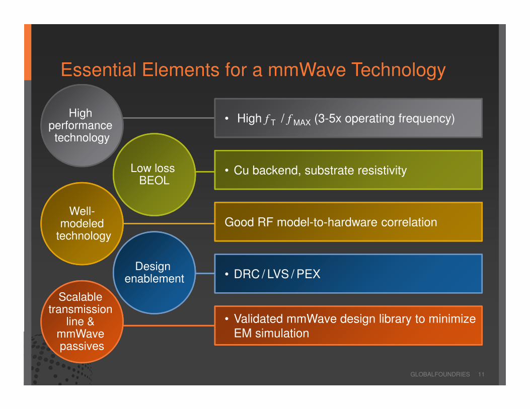
Essential Elements for a mmWave Technology
GLOBALFOUNDRIES 11
• High f T / f MAX (3-5x operating frequency)
• Cu backend, substrate resistivity
Good RF model-to-hardware correlation
• DRC / LVS / PEX
High performance technology
Low loss BEOL
Well-modeled
technology
Design enablement
Scalable transmission
line & mmWave passives
• Validated mmWave design library to minimize EM simulation

High Performance Technology
• f T / f MAX should be 3 - 5x application frequency
• SiGe achieves both high f T
and f MAX
• CMOS f T continues to increase with scaling, but f MAX peaks at
65-40nm nodes due to Rg*Cgd product
• SOI seems to show most promise at advanced nodes in continuing to drive increased RF performance with reduced impact from Rg*Cgd**
GLOBALFOUNDRIES 12
**Based on published data from multiple sources; multiple foundries included, but the data is not exhaustive. CMOS metrics are layout dependent (finger width, standard vs relaxed pitch, single vs. double gate contacts, number of contacts, metal levels, etc.)

Low Loss BEOL
Thin film transmission line with topside ground plane
Ground plane in BEOL prevents fields from entering substrate
Wavelength at 60GHz in SiO2 = 2.4mm; at 30GHz = 4.8mm
• Long transmission lines not uncommon
• Minimizing loss in BEOL is important
Availability of thick Cu levels and distance to ground planes are key to minimizing losses in BEOL
• Distance to ground plane may be difficult to achieve in advanced nodes
mmWave modeling and scalable mmWave structures help reduce the design risk
GLOBALFOUNDRIES 13

Scalable Transmission Lines & mmWave Passives
• Microstrip and co-planar, single and coupled wires, with optional side shielding
• Full suite of microstripdiscontinuities (mmWave passives)
• Scalable model / pcell: geometries and metal options
• Both time and frequency domain simulations
GLOBALFOUNDRIES 14
C
L∞
∆L1
∆R1
∆Ln
∆Rn
Ro
Skin effect circuit to capture high frequency effects
T-Line
Model
Topology
bend tee step taper gap short open
radial stub
yjunction
Excellent
Model-to-E-M
Field Solver
Agreement

RF SOI for 5G
GLOBALFOUNDRIES 15

Why RF SOI?
Device stacking:• Overcomes silicon Johnson Limit• Improved efficiency vs. power
combining
Substrate benefits for RF:• Reduced parasitics → higher Q,
lower loss and better noise figure• Increased isolation / linearity
Logic and control integration:• Potential for SOC integration
Low cost:• Excellent balance between
performance and integration
Mainstream silicon manufacturing:• Readily available capacity
GLOBALFOUNDRIES 16
Source: FDSOI and RFSOI Forum – February 27, 2015

RF SOI for mmWave Applications
SOI has been extensively evaluated for mmWave building blocks:
• Measured peak f T is 264GHz for a 30 X 1007nmsingle-gate contact, relaxed-pitch transistor
• Best f MAX of 283GHz is achieved by a 58 X 513nmsingle-gate contact regular pitch transistor
GLOBALFOUNDRIES 17
Source: O. Inac, M. Uzunkol and G. Rebeiz, “45-nm CMOS SOI Technology Characterization for Millimeter-Wave Applications”

Published results (45nm SOI):
1. “Millimeter-Wave Power Amplifiers in 45nm CMOS SOI Technology”, Jing-Hwa Chen, Sultan R. Helmi and Saeed Mohammadi
2. “28GHz >250mW CMOS Power Amplifier Using Multigate-Cell Design, Jefy A. Jayamon, James F. Buckwalter and Peter M. Asbeck, CICS 2015
3. “A 34% PAE, 18.6dBm 42-45GHz Stacked Power Amplifier in 45nm SOI CMOS” Amir Agah, Hayg Dabag, Bassel Hanafi, Peter Asbeck, Lawrence Larson and James Buckwalter
4. “High-Efficiency Microwave and mm-Wave Stacked Cell CMOS SOI Power Amplifiers”, Sutlan R. Helmi, Jing-Hwa Chen and Saeed Mohammadi, TMM 2015
Source: “A Broadband Stacked Power Amplifier in 45-nm CMOS SOI Technology”, Jing-Hwa Chen, Sultan R. Helmi, Reza Azedegan, Farshid Aryanfar and Saeed Mohammadi.
RF SOI mmWave Power Amplifier Design
SOI enables transistor stacking for superior RF PA:
• Stacked configuration has higher power-added efficiency & smaller chip area vs. bulk CMOS:
– Buried-oxide layer electrically isolates transistors, mitigating substrate leakage / breakdown
– Configuration has higher input and output impedances for matching networks with lower loss & higher bandwidth
• Parasitic capacitances to substrate are significantly reduced, minimizing phase & voltage swing imbalance
GLOBALFOUNDRIES 18
Source Frequency range PAE Saturated output power
1 27 to 39GHz 33% @ 32GHz 22.4 dBm
2 25 to 35GHz 29% @ 29GHz 24.5 dBm
3 42 to 45GHz 34% @ 42.5 GHz 19.4 dBm
4 42 to 54GHz 42% @ 46GHz 22.4 dBm

54dB @ 25GHz
PE42524 ISOLATIONPE42524 INSERTION LOSS
Breaking High-Frequency Barriers in RF SOI
GLOBALFOUNDRIES 19
Source: Peregrine supplied information
• Broadband frequency performance from 10MHz to 40GHz
• Highest linearity switch @ 40GHz
• Industry leading port-to-port isolation
• High reliability compared to GaAs & PIN alternatives (2KV HBM ESD)

RF SOI mmWave RF Switch Design
RF SOI enables transistor stacking for superior RF switch performance:
• Buried-oxide layer electrically isolates transistors, mitigating substrate leakage
• Junction capacitors are much smaller
• Linearity is enhanced
• Optimizing for insertion loss is simpler
• 3-4 stack 45nm RFSOI switches are sufficient to meet the 24dBm power level with 25dBm isolation
GLOBALFOUNDRIES 20
1. Source: M. Parlak, J.F. Buckwalter,“A 2.5-dB Insertion Loss, DC-60 GHz CMOS SPDT Switch in 45-nm SOI”CSICS 2011
Source: M. Parlak, J.F. Buckwalter,“A 2.5-dB Insertion Loss, DC-60 GHz CMOS SPDT Switch
in 45-nm SOI”CSICS 2011
Published results (45nm):
Source Frequency Insertion Loss Isolation IIP3
1 45GHz 1.7 dB >25 dB 18.2 dBm
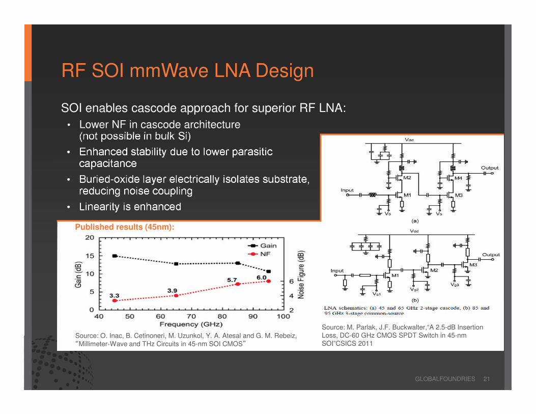
RF SOI mmWave LNA Design
SOI enables cascode approach for superior RF LNA:
• Lower NF in cascode architecture (not possible in bulk Si)
• Enhanced stability due to lower parasitic capacitance
• Buried-oxide layer electrically isolates substrate, reducing noise coupling
• Linearity is enhanced
GLOBALFOUNDRIES 21
Source: M. Parlak, J.F. Buckwalter,“A 2.5-dB Insertion
Loss, DC-60 GHz CMOS SPDT Switch in 45-nm
SOI”CSICS 2011Source: O. Inac, B. Cetinoneri, M. Uzunkol, Y. A. Atesal and G. M. Rebeiz,
“Millimeter-Wave and THz Circuits in 45-nm SOI CMOS”
Published results (45nm):

High Data Rate Sampling Converter Core in SOI
Dual channel high speed ADC for high data-rate communications & radar applications:
• 1024-bit CMOS output
• 42 to 68 GS/s conversion sampling rate
• 8-bit resolution
• Ultra-wide BW: 20GHz typical
• ± 0.8-bit differential nonlinearity
• ± 1.5-bit integral nonlinearity
• 5.8 bit ENOB to FS/4
• 0°C to +105°C Tj
• 2.3µ x 3.3µ core (32nm)
GLOBALFOUNDRIES 22
Source: Jariet datasheet, Rubicon-2 ADC macro

FD-SOI Body-Biasing Enables Power/Performance Trade-Off and Tuning of RF/Analog Parameters
GLOBALFOUNDRIES 23
� Forward BB (FBB) enables low voltage operation without speed loss
� Reverse BB (RBB) enables low leakage down to 1pA/micron
� Dynamic body biasing enables tuning RF/Analog characteristics: gM, gDS, self-gain, fT, fMAX
� Body biasing is an effective knob to tune RF performance characteristics

RF SOI and the Road to 300mm
GLOBALFOUNDRIES is 1st foundry to qualify and ramp a 300mm RF SOI technology into high-volume manufacturing:
• Long history of SOI manufacturing at 45nm and 32nm
• Development/ramp of customized RFSOI process (Peregrine UltraCMOS 11™)
300mm RF SOI substrates provide benefits:
• Improved starting substrate uniformity
• Availability of stressor materials for lower Ron
• Availability of low-K materials for improved Coff
300mm RF SOI manufacturing provides advantages:
• Increased wafer productivity: ~2.3x over 200mm
• Improved edge yield for larger die sizes; reduced periphery over 200mm
• Reduced assembly cost per die; 10-15% bump/CSP cost advantage per die compared to 200mm
Seamless transition to next generation RF processes:
• Creates learning on advanced tools which can be leveraged for next gen roadmaps
GLOBALFOUNDRIES 24
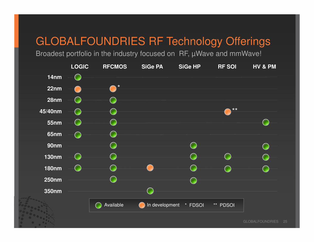
GLOBALFOUNDRIES RF Technology Offerings
GLOBALFOUNDRIES 25
Broadest portfolio in the industry focused on RF, µWave and mmWave!
LOGIC RFCMOS SiGe PA SiGe HP RF SOI HV & PM
14nm
22nm
28nm
45/40nm
55nm
65nm
90nm
130nm
180nm
250nm
350nm
Available In development * FDSOI ** PDSOI
*
**

GLOBALFOUNDRIES 26
GLOBALFOUNDRIES Worldwide Manufacturing and Support
East Fishkill,New York
East Fishkill,New York
Malta,New York
Malta,New York
Burlington,Vermont
Burlington,Vermont
SingaporeSingaporeDresden,GermanyDresden,Germany
5 manufacturing centers on 3 continents
Localized technical support

Partnering for Success
GLOBALFOUNDRIES 27
Engagement
• Business development
• Product marketing
• Field sales
Development
• Field applications
• Technical support
• Process development
• PDK / modeling
Design & Front-end
Services
• Foundational libraries & IP
• Third party design houses
• Alternative simulator support
• MPWs and prototyping
NPI & Manufacturing
• Customer engineering
• Reliability / failure analysis
• Skew lots and device “striping”
• Program management
Back-end Services
• Packaging: 2D / 2.5D / 3D
• Test

Summary
5G standards definition and requirements are continuing to evolve
Millimeter wave operation for 5G poses both opportunities and challenges from a technology and design perspective…
Significant R&D has been done in evaluating the application of SOI to 5G architectures, with very positive results
GLOBALFOUNDRIES is ready
GLOBALFOUNDRIES 28
Current thinking suggests millimeter
wave spectrum may be in play
Phased arrays and beamforming are
enabling technologies to deliver on 5G
promises
SOI holds great promise in delivering
on the key requirements of 5G systems
Long history of SOI development and
high-volume manufacturing, with a
technology roadmap and support
model aligned with the needs of the
market & our customers

Trademark Attribution
GLOBALFOUNDRIES®, the GLOBALFOUNDRIES logo and combinations thereof, and GLOBALFOUNDRIES’ other trademarks and service marks areowned by GLOBALFOUNDRIES Inc. in the United States and/or other jurisdictions. All other brand names, product names, or trademarks belong to their respective owners and are used herein solely to identify the products and/or services offered by those trademark owners.
© 2016 GLOBALFOUNDRIES Inc. All rights reserved.
Thank [email protected] +001.408.479.1143