rf & mmw in virtusnews.ntu.edu.sg/rc-virtus/documents/2015-prof boon chirn... · 2015. 8....
TRANSCRIPT

RFIC for Mobile Wireless Communication
RFIC for Vehicular Communication and Radar
RF & MMW in VIRTUS
Assoc. Professor Boon Chirn ChyeProgramme Director, RF & MM-wave, VIRTUS, NTUAssoc. Editor, IEEE Transaction of VLSI; EEE NTU Teaching Excellent Award 2012; Commendation Award for Teaching Excellence 2014.IEEE Electron Devices Letters Golden Reviewer.
Web: http://www.ntu.edu.sg/home/eccboon

Research Leadership
Funding Source Quantum ($) Role Grant Period
Huawei Tech. Co. Ltd-NTU Joint R&D:
10GiFi research & development of ultra-
wideband RF transceiver
S$927,840.00 PI 15th July 2014 to
14th July 2017
Tier 2: High Thermal Resolution Ultra-Low
Power Integrated Imager: Fund. Issues in
CMOS
S$885,352.00 PI July 2013 to June
2016
Project 17: Electronic Circuit Design,
Communications under SMART-IRG5: Low
Energy Electronic Systems (MIT-NTU)
S$836,400.00 for
year 2015 and
2016.
PI 1st April 2014 to
30th March 2016
Project 2: Electronic Circuit Design,
Communications under SMART-IRG5: Low
Energy Electronic Systems (MIT-NTU)
S$376,200.00 for
year 2014.
PI 1st April 2013 to
30th March 2014
Project 10: Electronic Circuit Design,
Communications under SMART-IRG5: Low
Energy Electronic Systems (MIT-NTU)
S$391,560.00 for
year 2013.
PI 1st April 2012 to
30th March 2013

Research Leadership
Funding Source Quantum ($) Role Grant Period
Project 10: Electronic Circuit Design,
Communications under SMART-IRG5: Low
Energy Electronic Systems (MIT-NTU)
S$391,560.00 for
year 2013.
PI 1st April 2012 to
30th March 2013
SMA (MIT-NTU) CMOS Front-end S$45,000.00 PI 5th August 2013
to 4th August
2017
SMA (MIT-NTU) High Speed CMOS S$45,000.00 PI 13th January
2014 to 12th
August 2018
ARC3/09: Batteryless Flexible Transceiver
for Biomedical Applications
S$1,186,270.00 PI May 2009 to July
2012
RG73/07: Ultra-low Power Fully Integrated
CMOS 24GHz Receiver
S$208,258.22 PI March 2008 to
October 2011.

Funding Source Quantum ($) Role Grant Period
NRF : An Ultra Low-Power RF Transceiver
Chip towards a New Paradigm of Life
Quality
S$250,000.00 Co-PI February 2009
to February
2010
University of Electronic Science and
Technology (UEST) of China-NTU Joint
R&D, jointly funded by UEST and NTU :
System-on-chip: Realization of Software
Radio
S$331,125.00 Co-PI 3 December
2008 to 2
December 2009
Agency for Science, Technology and
Research (A*STAR) : An Ultra Low-Power
RFIC Chip For Wireless and
Communication
S$1,210,020.00 Co-PI March 2006 to
February 2009
NRF : An Ultra Low-Power RF Transceiver
Chip towards a New Paradigm of Life
Quality
S$250,000.00 Co-PI February 2009
to February
2010
University of Electronic Science and
Technology (UEST) of China-NTU Joint
R&D, jointly funded by UEST and NTU :
System-on-chip: Realization of Software
Radio
S$331,125.00 Co-PI 3 December
2008 to 2
December 2009

World Fastest Consumer WiFi IEEE 802.11ax Integrated Circuit (IC) R&D

• D2D (Device-to-Device) communications using DSRC– to off-load the base stations in cellular networks– to improve response time
6
LEES: Motivation
* DSRC (Dedicated Short-Range Communication
*

LEES : Single Chip WiFi and D-2-D
AchievedNo. of patent
9 US Provisional Patents
1. P. Choi, C. C. Boon, L. S. Peh,“A High Efficiency WidebandCompact Power AmplifierModule”. STLO Ref: 15122S-LEES, June. 2015.
2. M. D. Mao, C. C. Boon, L. S.Peh, “A High EfficiencyWideband Compact PowerAmplifier Module”. STLO Ref:15122S-LEES, June. 2015.
New Invention Disclosures

8
LEES: Goal of 802.11p system: D2D
• Making use of an existing WiFi solution on a smartphone, combined with 802.11p front-end circuit
9
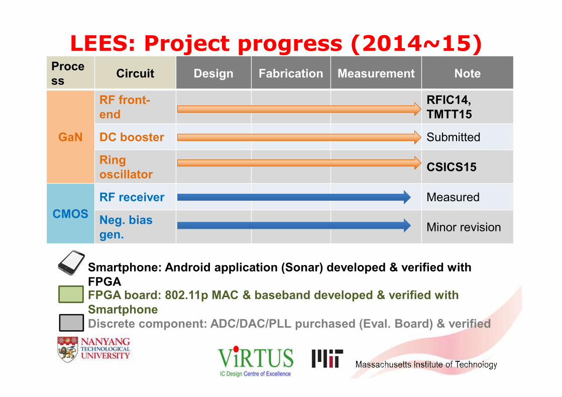
LEES: Project progress (2014~15)Process
Circuit Design Fabrication Measurement Note
GaN
RF front-end
RFIC14,TMTT15
DC booster Submitted
Ringoscillator
CSICS15
CMOS
RF receiver Measured
Neg. bias gen.
Minor revision
FPGA board: 802.11p MAC & baseband developed & verified with SmartphoneDiscrete component: ADC/DAC/PLL purchased (Eval. Board) & verified
Smartphone: Android application (Sonar) developed & verified with FPGA

10
LEES: CMOS bias gen. for D-GaN HEMT
(GF 0.18um CMOS)
• Fully integrated negative bias gen.
– 1.8V/3.3V input
– Negative voltage output
– Regulation to be revised
-1.68V @ 0.125MHz clock-2.70V @ 0.25MHz clock-5.17V @ 2MHz clock

11
LEES: High efficiency technique
Conventional Tx/Rx Switching Scheme
Proposed Tx/Rx Switching Scheme
� = ��� × 10� ��,���� ��⁄
���� = ����,�� − ��,����
� = ���
���� = ����,��
39.7% @ 794mW
(due to 1dB SPDT loss)
50% @ 1W
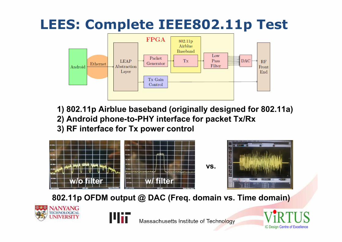
LEES: Complete IEEE802.11p Test
802.11p OFDM output @ DAC (Freq. domain vs. Time domain)
1) 802.11p Airblue baseband (originally designed for 802.11a)2) Android phone-to-PHY interface for packet Tx/Rx3) RF interface for Tx power control
w/o filter w/ filter
vs.

MMW High Gain Power Amplifier
IEEE 802.15.3c Power Amplifier
This work demonstrates an ILPA with largest injection locking bandwidth. The fabricated PA has achieved a injection locking range from 50 GHz to 59 GHz. Maximum output power of 11.39 dBm has been obtained while the highest PAE is 16.1 %. Moreover, the chip size is 260 μm x 400 μm excluding pads.

First 10+ Gb/s transmitter with fractional pre-emphasis (FPE) die photograph with ultra-compact active area
(a) First 10+ Gb/s transmitter with fractional pre-emphasis (FPE) die photograph with ultra-compact active area (0.0081 mm2).(b) Measured 12 Gb/s before channel pre-corrected using fractional pre-emphasis.(c) Measured 12 Gb/s after lossy channel showing excellent performance (4.05 ps RMS jitter, 24.89 ps Pk-to-Pk jitter and 87 mV vertical opening under 2^31-1 PRBS input).

Non-invasive Blood Glucose Detection
Continuous glucose monitoring systems (CGMS) is a necessary tool for the diabetics to monitor their glucose level and take preventive actions.
Patent filedNovel Comparable, Low cost, non-invasive methodology.
Ref. 0 Prototype:A total of 96 sample points indicate readings in Clarke grid A (26.66%) and B (73.34%) which is clinically acceptable.

Non-invasive Blood Glucose Detection
Compact Integrated Circuit Non-invasive Blood Glucose Detection (GF 65nm).
24hr blood glucose detection.
Android Apps instant report.Cloud connection for report and data transfer to hospital.
An Asynchronous 10-Bit 12.5% Redundant 200 Msps SAR ADC WITH BUILT IN ERROR CORRETION(0.7fF unit cap )
Solution for noisy environment.As it is difficult to build high resolution high speed ADC due to
imperfection (in components for example).

An Asynchronous 10-Bit 12.5% Redundant 200 Msps SAR ADC WITH BUILT IN ERROR CORRETION(0.7fF unit cap )
• 12.5% Redundancy• Error Correction- Can
correct up to 3 incorrect decisions in 1 conversion cycle
• Relaxes Reference Buffer Settling Time/Power Consumption
• Finishes 10bit Conversion in 9 cycles
• Bottom Plate Sampling• 0.7fF MOM Unit Capacitor

Thank you for your time and effort to understand my work. Web: http://www.ntu.edu.sg/home/eccboon