rf mems devices prof. dr. wajiha shah. outline use of rf mems devices in wireless and satellite...
TRANSCRIPT

RF MEMS devices
Prof. Dr. Wajiha Shah
OUTLINE
Use of RF MEMS devices in wireless and satellite communication system.
1. MEMS variable capacitor (tuning range : 280%)
2. MEMS tunable inductor
3. MEMS multiport switch (using range : > 20GHz)
Introduction (1)
The MEMS technology has the potential of replacing many RF components used in today’s mobile communication and satellite system.
Advantage of MEMS 1. can reduce the size, weight, power consumption
and component counts. 2. promise superior performance. 3. can be built with low cost, mass producibility and high reliability. 4. new functionality and system capability.
MEMS variable capacitors (1)
MEMS technology has the potential of realizing variable capacitors with a performance that is superior to varactor diodes in areas such as non-linearity and losses.
Over the past, variable capacitors was theoretical tuning range of 50% - 100%, in practice, the capacitor operate over a smaller tuning range away from the collapse voltage.
Proposed MEMS capacitor Fig. 1 illustrates a schematic diagram.
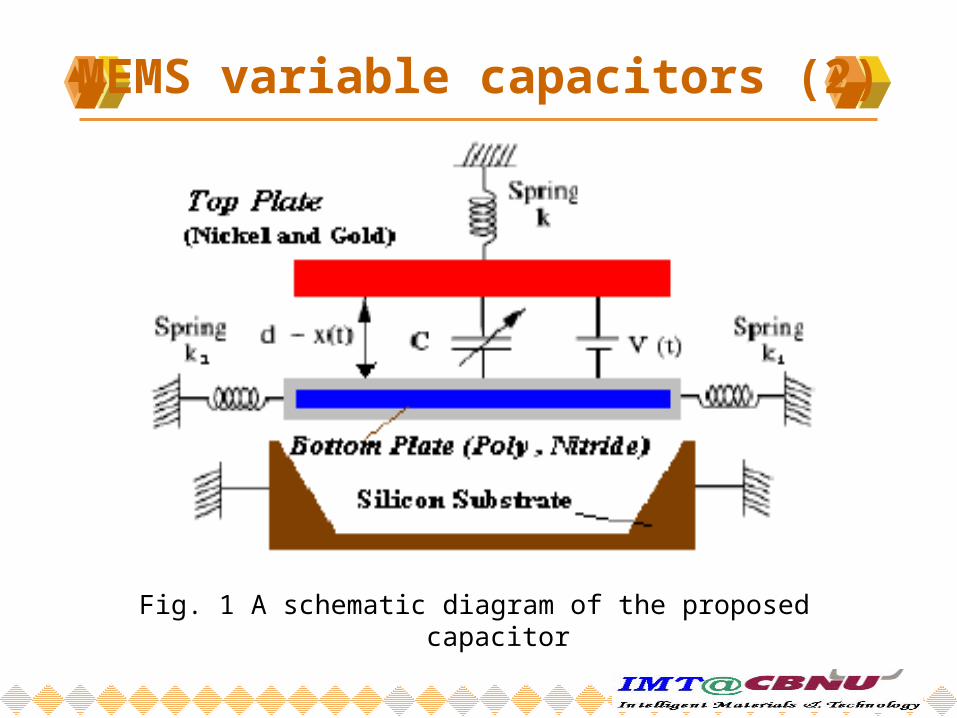
MEMS variable capacitors (2)
Fig. 1 A schematic diagram of the proposed capacitor
MEMS variable capacitors (3)
It consists of two movable plates with an insulation dielectric layer on top of the bottom plate.
With the two plates being flexible, makes it possible for the two plates to attract each other and decrease the maximum distance before the pull-in voltage occurs.
Construction of proposed capacitor Two structural layers, three sacrificial layers, and two insulating layers of Nitride.
MEMS variable capacitors (4)
The top plate is fabricated from nickel with a thickness of 24 ㎛ covered by a gold layer of thickness 2 ㎛ .
The bottom plate is made of polysilicon covered by a Nitride layer of a thickness of 0.35 ㎛ .
============================================
Making process Metal MUMPs (Multi-User MEMS Process) Simulation Coventor Ware
MEMS variable capacitors (5)
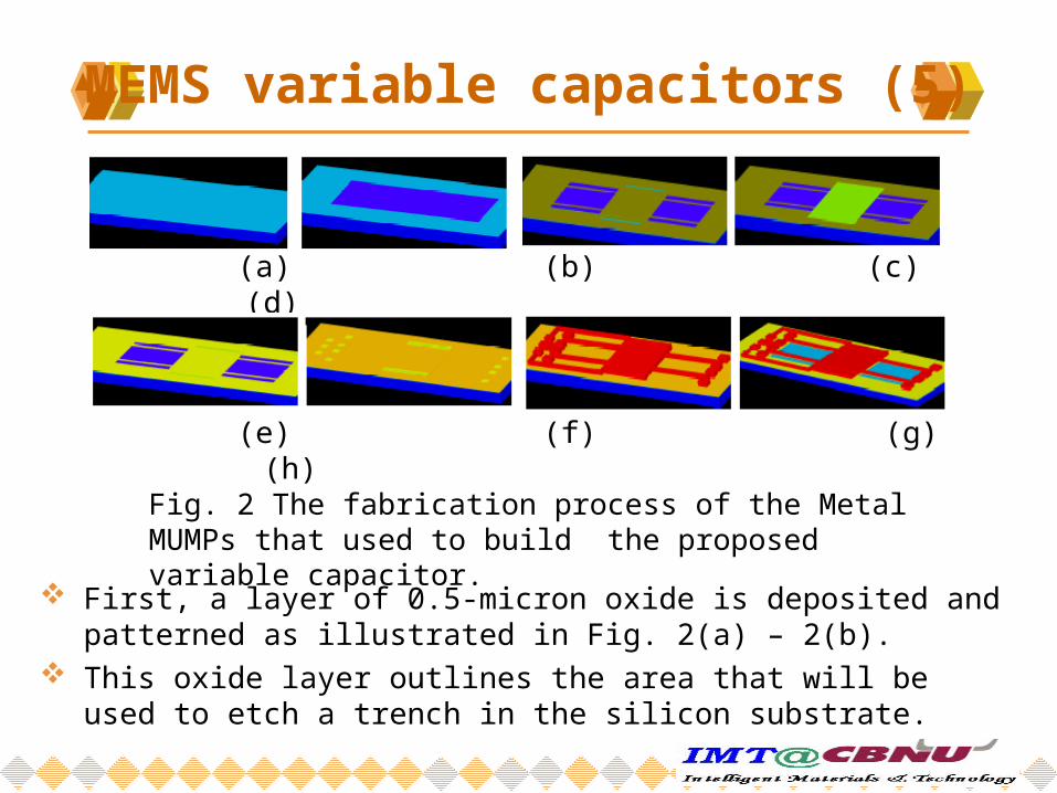
(a) (b) (c) (d)
(e) (f) (g) (h)
First, a layer of 0.5-micron oxide is deposited and patterned as illustrated in Fig. 2(a) – 2(b).
This oxide layer outlines the area that will be used to etch a trench in the silicon substrate.
Fig. 2 The fabrication process of the Metal MUMPs that used to build the proposed variable capacitor.
MEMS variable capacitors (6)
The first Nitride layer of 0.35-micron thickness is deposited and patterned as illustrated in Fig. 2(c).
This Nitride layer forms the bottom cover of the polysilicon layer and is used as a part of the capacitor’s bottom plate.
On top of the first Nitride layer, a 0.7-micron layer of polysilicon is deposited and patterned to form the bottom conductive plate of the variable capacitor. 2(d)
The last step in building the bottom plate of the variable capacitor is to deposit the second Nitride layer on top of the polysilicon layer to form the isolating area that prevents any electrical contact between the two plates.
MEMS variable capacitors (7)
A 1.1-micron layer of second oxide is then deposited as illustrated in Fig. (f). The second oxide layer is etched so that the metal layer is anchored on the Nitride and a physical contact between the bottom electrode (Poly-silicon) and the two outer pads is ensured.
The last layer is metal layer, which is formed of a 24 ㎛of Nickel with 2 ㎛ of gold on top of the Nickel layer.
The last step is to etch out the sacrificial layers as well as to etch a trench in the silicon substrate. The trench etch of the substrate is determined by the first oxide layer.
MEMS variable capacitors (8)
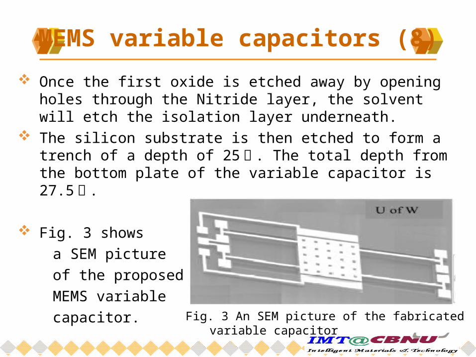
Once the first oxide is etched away by opening holes through the Nitride layer, the solvent will etch the isolation layer underneath.
The silicon substrate is then etched to form a trench of a depth of 25 ㎛ . The total depth from the bottom plate of the variable capacitor is 27.5 ㎛ .
Fig. 3 shows a SEM picture of the proposed MEMS variable capacitor. Fig. 3 An SEM picture of the fabricated variable capacitor
MEMS variable capacitors (9)
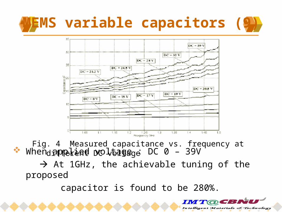
When applied voltage : DC 0 – 39V At 1GHz, the achievable tuning of the proposed capacitor is found to be 280%.
Fig. 4 Measured capacitance vs. frequency at different DC voltage
MEMS tunable inductors (1)
High-Q inductors find widespread use in RF transceivers circuits.
The availability of tunable inductor circuits to circumvent, construct filter for frequency
agile applications
Before variable inductors have been achieved by using drive coil coupled to the RF inductor.
use of mutual inductance and 100% tuning range However, this technique requires the use of an
additional drive circuit to change the phase of the current in the drive coil.
MEMS tunable inductors (2)
A λ/4 transmission line was used to construct the inverter. The inverter has a limited bandwidth and would relatively occupy a large area in low frequency applications.
MEMS tunable inductor is proposed using lumped element inverters.
advantage : wider bandwidth, more design flexibility
The circuit representing the tunable inductor consists of two inductors, two fixed capacitor and a shunt variable capacitor.
The fabricated variable inductor chip is given in Fig. 5.
MEMS tunable inductors (3)
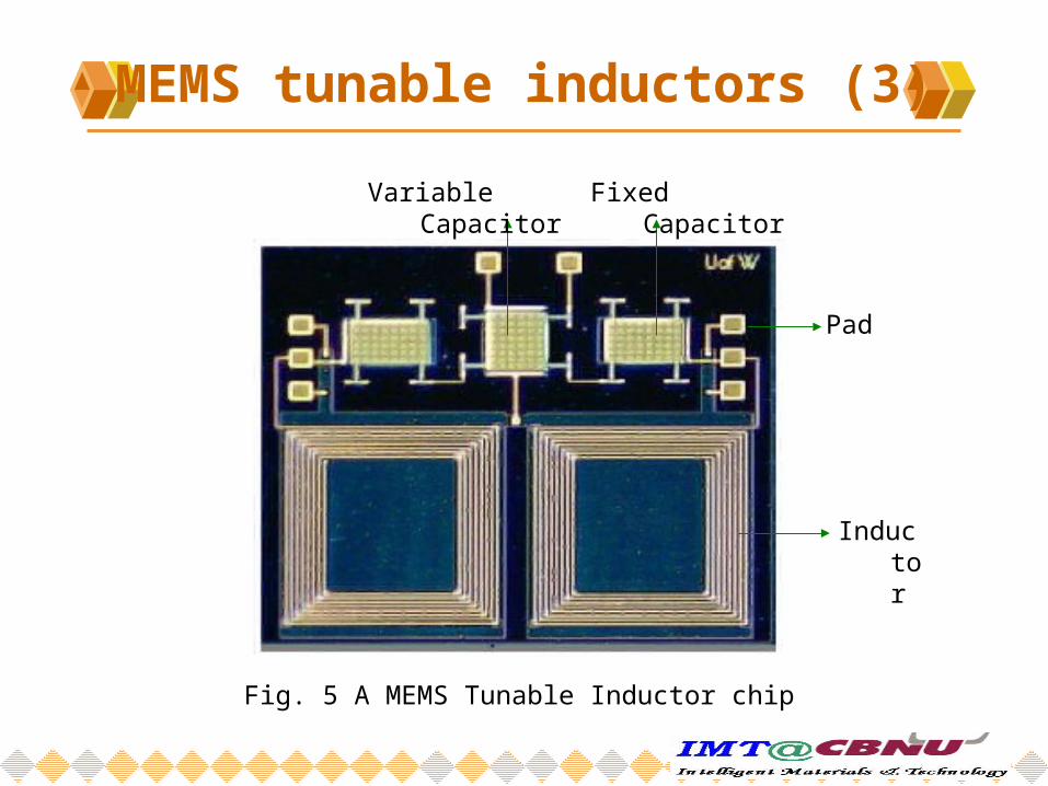
Fig. 5 A MEMS Tunable Inductor chip
Variable Capacitor Fixed Capacitor
Pad
Inductor
MEMS tunable inductors (4)
The MUMPs process includes three layers of polysilicon (poly0, poly1, poly2), two layers of oxide, one layer of gold.
The gold layer is deposited on the top polysilicon layer (poly2).
The poly0, first oxide, poly1, second oxide, poly2 and gold have thickness of 0.5, 2.0, 2.0, 0.75, 1.5 and 0.5 ㎛ respectively.
The two parallel plate variable capacitor 1. lower plate : poly1 air gap (0.75 ㎛ ) upper plate : poly2 2. C : 2.05pF, Area : 210*270 ㎛ 2
MEMS tunable inductors (5)
The fixed capacitors are constructed using the same concept except that no voltage source will be applied to the plates. (C : 1.76pF, Area : 200*280 ㎛2)
There are 8 pads used in this design : one for the DC voltage, one for ground and 6 pads for the coplanar RF input and output signals. (material : poly2, gold)
There pads have a significant low parasitic capacitance of 0.25pF. (Area : 86*86 ㎛ 2)
RF MEMS multiport switch (1)
Microwave switch 1. Mechanical-type (coaxial & waveguide) 2. Semiconductor-type (PIN diode & FET)
MEMS switches promise to combine the advantageous properties of both mechanical and semiconductor switches.
Most of the research effort reported in literature has been directed toward the development of Single-Pole-Single-Through (SPST) switches.
RF MEMS multiport switch (2)
An integrated SP3T MEMS switch. Three beams with narrow-width tips are integrated on top of a coplanar transmission line.
The junction where the three beams interact is inherently a wide band junction, which make it possible to design a wideband SP3T switch with 30dB isolation up to 20GHz.
The mechanical design of the switch is analyzed using Coventor-Ware.
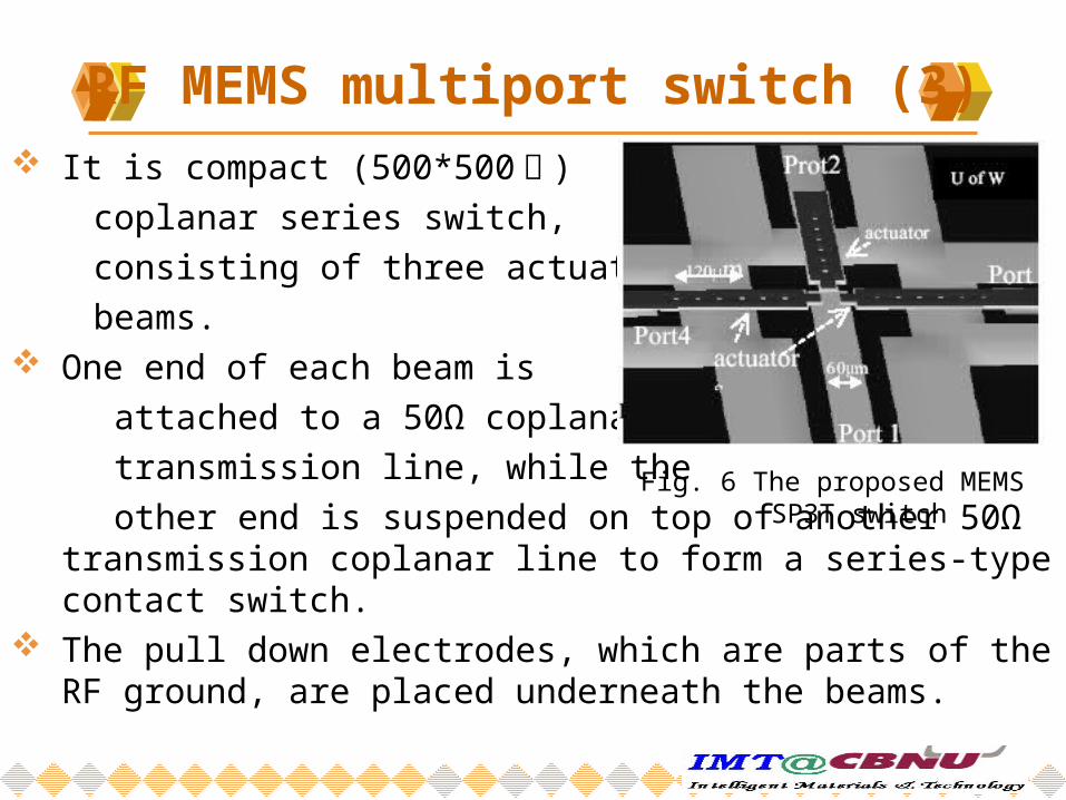
RF MEMS multiport switch (3) It is compact (500*500 ㎛ ) coplanar series switch, consisting of three actuating beams. One end of each beam is attached to a 50Ω coplanar transmission line, while the other end is suspended on top of another 50Ω
transmission coplanar line to form a series-type contact switch.
The pull down electrodes, which are parts of the RF ground, are placed underneath the beams.
Fig. 6 The proposed MEMS SP3T switch
RF MEMS multiport switch (4)
Alternatively, the SP3T switch can be implemented in a hybrid-form where the beams are micro-machined separately and then integrated on an Alumina substrate using flip-chip technology.
The beams are fabricated using the Multi-User MEMS Process surface micro machining.
Each beam is made of a Polyilicon layer of a thickness of 1.5 ㎛ coverd by a gold layer of 0.5 ㎛thick.
Release holes are accommodated for HF accessibility to the trapped oxide under the beams.
RF MEMS multiport switch (5)
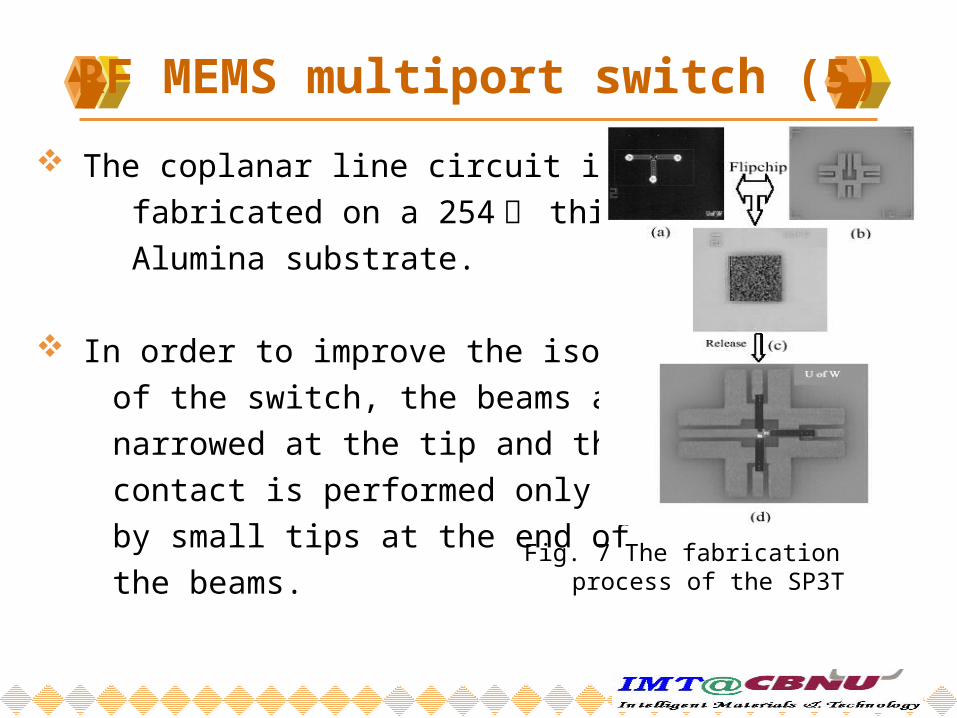
The coplanar line circuit is fabricated on a 254 ㎛ thick Alumina substrate.
In order to improve the isolation of the switch, the beams are narrowed at the tip and the contact is performed only by small tips at the end of the beams.
Fig. 7 The fabrication process of the SP3T
RF MEMS multiport switch (6)
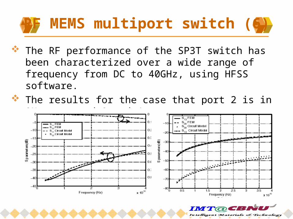
The RF performance of the SP3T switch has been characterized over a wide range of frequency from DC to 40GHz, using HFSS software.
The results for the case that port 2 is in ON state and 3 and 4 are in OFF state are shown in Fig. 8.

T h e e n d