rf & comm handbook - national...
TRANSCRIPT

RF & Communications Handbook

Copyright
© 2007 National Instruments Corporation. All rights reserved.
Under the copyright laws, this publication may not be reproduced or transmitted in any form, electronic or
mechanical, including photocopying, recording, storing in an information retrieval system, or translating, in whole
or in part, without the prior written consent of National Instruments Corporation.
National Instruments respects the intellectual property of others, and we ask our users to do the same. NI
software is protected by copyright and other intellectual property laws. Where NI software may be used to
reproduce software or other materials belonging to others, you may use NI software only to reproduce materials
that you may reproduce in accordance with the terms of any applicable license or other legal restriction.
Trademarks
National Instruments, NI, ni.com, and LabVIEW are trademarks of National Instruments Corporation. Refer to the
Terms of Use section on ni.com/legal for more information about National Instruments trademarks.
Other product and company names mentioned herein are trademarks or trade names of their respective
companies.
Members of the National Instruments Alliance Partner Program are business entities independent from National
Instruments and have no agency, partnership, or joint-venture relationship with National Instruments.
Patents
For patents covering National Instruments products, refer to the appropriate location: Help»Patents in your
software, the patents.txt file on your CD, or ni.com/legal/patents.
Worldwide Technical Support and Product Information
ni.com
National Instruments Corporate Headquarters
11500 North Mopac Expressway · Austin, Texas · 78759-3504 USA · Tel: (512) 683-0100
Worldwide Offices
Australia 1800 300 800, Austria 43 0 662 45 79 90 0, Belgium 32 0 2 757 00 20, Brazil 55 11 3262 3599,
Canada 800 433 3488, China 86 21 6555 7838, Czech Republic 420 224 235 774, Denmark 45 45 76 26 00,
Finland 385 0 9 725 725 11, France 33 0 1 48 14 24 24, Germany 49 0 89 741 31 30, India 91 80 41190000,
Israel 972 0 3 6393737, Italy 39 02 413091, Japan 81 3 5472 2970, Korea 82 02 3451 3400,
Lebanon 961 0 1 33 28 28, Malaysia 1800 887710, Mexico 01 800 010 0793, Netherlands 31 0 348 433 466,
New Zealand 0800 553 322, Norway 47 0 66 90 76 60, Poland 48 22 3390150, Portugal 351 210 311 210,
Russia 7 495 783 68 51, Singapore 1800 226 5886, Slovenia 386 3 425 42 00, South Africa 27 0 11 805 8197,
Spain 34 91 640 0085, Sweden 46 0 8 587 895 00, Switzerland 41 56 200 51 51, Taiwan 886 02 2377 2222,
Thailand 662 278 6777, United Kingdom 44 0 1635 523545

Contents
Communication Systems Overview .................................................................................................................... 5
RF Terms and Measurements ............................................................................................................................. 8
Spectral Analysis ........................................................................................................................................................ 8
Resolution Bandwidth and Dynamic Range .............................................................................................................. 8
Resolution Bandwidth (RBW) ............................................................................................................................... 8
Noise Floor ............................................................................................................................................................ 9
Dynamic Range ................................................................................................................................................... 10
Spectral Measurements .......................................................................................................................................... 10
Power in Band ..................................................................................................................................................... 10
Occupied Bandwidth ........................................................................................................................................... 11
Adjacent Channel Power ..................................................................................................................................... 11
Harmonic Distortion ........................................................................................................................................... 12
Calculating Harmonic Distortion ..................................................................................................................... 13
Testing for Harmonic Distortion ..................................................................................................................... 14
Modulation ....................................................................................................................................................... 15
Mathematical Representation of Modulation ........................................................................................................ 15
Digital vs. Analog Modulation ................................................................................................................................. 15
Visualization of a Modulated Signal ........................................................................................................................ 16
Analog Modulation .................................................................................................................................................. 16
Types of Analog Modulation ............................................................................................................................... 17
Amplitude Modulation (AM) .......................................................................................................................... 17
Frequency Modulation (FM) ........................................................................................................................... 26
Phase Modulation (PM) .................................................................................................................................. 34
Digital Modulation................................................................................................................................................... 36
Introduction to IQ Signals ................................................................................................................................... 36
Mathematical Background ............................................................................................................................. 36
In-phase and Quadrature-phase components ............................................................................................... 37
The IQ Representation and Modulation ......................................................................................................... 40
Advantages of using IQ ................................................................................................................................... 43
Mapping Bits to Symbols .................................................................................................................................... 44
Bits, Symbols, and Rate .................................................................................................................................. 46
Types of Digital Modulation ................................................................................................................................ 47
Amplitude Shift Keying (ASK) .......................................................................................................................... 47
Frequency Shift Keying (FSK) .......................................................................................................................... 49
Phase Shift Keying (PSK) ................................................................................................................................. 55
Quadrature Amplitude Modulation (QAM) .................................................................................................... 61
Hardware Labs .................................................................................................................................................. 67
Introduction to PXI Hardware ................................................................................................................................. 67
Overview and Background on PXI ....................................................................................................................... 67
PXI Features, Technologies and Benchmarks ..................................................................................................... 69
Introduction to the National Instruments RF and Communications Platform .................................................... 73

Overview of RF VSA, VSG, CW, Switching and Preamp Modules ........................................................................ 74
RF & Communications Test Development Software ........................................................................................... 75
Summary ............................................................................................................................................................. 76
Additional Resources .......................................................................................................................................... 76
Hardware Configuration .......................................................................................................................................... 77
Configuring the NI PXI-5660 ................................................................................................................................ 77
Index ................................................................................................................................................................ 84

National Instruments RF & Communications Handbook, Page 5 24/09/2007 00:59:52, Copyright © 2007 National Instruments Corporation
Communication Systems Overview
From the present-day internet to the old-fashioned radio and black & white television, communication
systems form the backbone of many commonly used applications. The requirements of a
communications system vary based on their application. Some constraints that can factor into the
design of a communication system include:
Cost
Power requirements
Reliability
Range of communication needed
Speed / Data Rate
Conformance with Standards
These and other factors mean that the elements of a communication system can differ greatly from one
system to another. For instance, a garage door opener or remote keyless entry on an automobile will
need transfer speeds that are barely a fraction of what is required by optical fibers that support the
internet infrastructure.
Communication systems can be broadly classified as analog or digital based on the nature of the
message being transmitted. Again, depending on the application, either an analog or digital system
might be the preferred way to communicate. Even within digital communication systems, for example,
the implementation of the transmitter and receiver can vary tremendously.

RF & Communications Handbook, Page 6 Copyright © 2007 National Instruments Corporation 00:59:52 24/09/2007,
Real
RealRealIQ
IQ Real RealBitsBitsBits
Bits Bits Bits
Up
co
nv
ers
ion
to
IF
Dig
ita
l to
An
alo
g
Co
nv
ers
ion
Up
co
nv
ers
ion
to
RF
De
mo
du
lati
on
Do
wn
co
nv
ers
ion
fro
m IF
An
alo
g t
o D
igit
al
Co
nv
ers
ion
Do
wn
co
nv
ers
ion
fro
m R
F
Ch
an
ne
l C
od
ing
Ch
an
ne
l
De
co
din
g
So
urc
e
De
co
din
gS
ou
rce
Co
din
g
Mo
du
lati
on
Receive Path
Transmit Path
Channel
Real
Figure 1, Elements that you might find in a digital communications system.
Figure 1 illustrates some components that are commonly found in a digital communication system. The
arrows depict the direction in which signals propagate. On the Transmit Path, the message generated at
the transmitter undergoes some processing - source coding through upconversion - before transmission
occurs. The transmitted signal then goes through a communication channel that may add noise or other
impairments. At the receiver, the signal again needs to be processed – downconversion through source
decoding - before the original message can be recovered.
The blocks on the Transmit Path, the top row of Figure 1, represent elements that you might find in a
digital transmitter. These elements include:
Source Coding: Bits that represent the message to transmit are input to this block, which applies
a source coding algorithm to create a more compact representation. It does so by exploiting
redundant information in the input bits. A typical example of a source-coding application is the
popular ‘zip’ file format commonly used to compress larger files, reducing size in order to reduce
storage space or transmission requirements.
Channel Coding: Encodes input bits to create a bit stream that is more robust to noise and
errors caused by the communication channel. The block systematically adds redundancy to
achieve this resulting in the output of this block generally being larger than the block input.
Modulation: Converts the bits to a sampled (discrete-time) signal – a format that is more
suitable for transmission over the communication channel. The signal samples output by the
Modulation block are often referred to as “baseband” signal samples. These samples are
complex-valued numbers that represent a discrete-time signal with frequency content centered
at zero.
Upconversion to IF: Converts the output of the modulation block to a higher, intermediate
frequency (IF) in preparation for transmission. More specifically, the block output is a sampled IF
signal represented by real-valued numbers.

RF & Communications Handbook, Page 7 Copyright © 2007 National Instruments Corporation 00:59:52 24/09/2007,
Digital to Analog Conversion (DAC): Converts the IF signal samples to an analog (continuous-
time) signal.
Upconversion to RF: Generates the signal to be transmitted by converting the output of the DAC
block to a radio frequency (RF) signal.
The blocks on the bottom row of Figure 1 represent elements that you might find in a digital receiver,
which is sometimes thought of as the mirror image of the transmitter. These include:
Downconversion from RF: Converts the received RF signal to a lower-frequency signal.
Specifically, the output of this block is an analog IF signal. There may be some additional
processing elements here to filter out noise or unwanted signal components from the IF signal.
Analog to Digital Conversion (ADC): Converts the analog IF signal to IF signal samples.
Downconversion from IF: Converts the IF signal samples to baseband signal samples.
Demodulation: Decodes the baseband signal samples to determine the bit pattern that was
modulated. In the absence of errors, the output should match the input to the modulation block
at the transmitter.
Channel Decoding: Decodes the input bits to detect and/or recover any bits that were received
in error due to noise or impairments. In the absence of errors, the output should match the
input to the channel encoding block at the transmitter.
Source Decoding: Decodes the output of the channel decoding block to recover the original
digital message.

RF & Communications Handbook, Page 8 Copyright © 2007 National Instruments Corporation 00:59:52 24/09/2007,
RF Terms and Measurements
Spectral Analysis
Spectral Analysis involves examining the frequency-domain content of a signal. In doing so, you consider
a signal as being composed of a sum of sinusoidal components. The basis for such analysis is the Fourier
theorem, which states that any waveform in the time domain (that is, one that you can see on an
oscilloscope) can be represented by the weighted sum of sines and cosines. The "sum" waveform in
Figure 2 is actually composed of individual sine and cosine waves of varying frequency. The same "sum"
waveform appears in the frequency domain as amplitude and phase values at each component
frequency (that is, f0, 2f0, 3f0).
Figure 2, Spectral analysis involves examination of the frequency components that make up a signal. The signal marked ‘sum’ is the sum of three frequency components, the f0, 2f0, 3f0 signals.
Resolution Bandwidth and Dynamic Range
Two parameters that are fundamental to spectral analysis are resolution bandwidth and dynamic range.
Resolution bandwidth helps to determine the frequency accuracy of a measurement. Dynamic range
helps to determine the amplitude accuracy of a spectral measurement.
Resolution Bandwidth (RBW)
Resolution Bandwidth (RBW) is the smallest frequency that can be resolved on a power spectrum. In a
traditional swept-tuned spectrum analyzer, the RBW is a physical filter in hardware through which the
RF signal is swept. This is the reason swept-tuned spectrum analyzers have discrete RBW filter settings
such as 1 MHz, 100 kHz, 10 kHz, 1 kHz, and 100 Hz. As we will see, RBW is also useful when considering
the operation of modern computer-based spectrum analyzers that typically apply a Fast Fourier
Transform (FFT) algorithm to examine the frequency spectrum of a signal.

RF & Communications Handbook, Page 9 Copyright © 2007 National Instruments Corporation 00:59:52 24/09/2007,
Figure 3, The effect of RBW settings on a spectrum for a signal with three distinct frequency components.
Figure 3 shows the effect of smaller RBW on a spectrum for a signal that contains three distinct
frequency components. RBW becomes smaller as we move from the leftmost to rightmost image in the
figure. Notice that smaller RBW values offers finer spectral resolution, allowing the tones to be
distinguished from each other. The smaller RBW on the right has much higher resolution and allows the
lower-level sidebands / spurs to be visible. Since frequency resolution of an FFT is based upon the time
duration of the data supplied to the FFT, a lower RBW requires a longer acquisition time. This leads to
the tradeoff for better frequency resolution. When acquisition time is a factor and the display needs to
be updated rapidly, or when the modulation bandwidth is fairly wide, a higher RBW can be used.
Also notice that as the RBW decreases, so does the noise floor. Every factor of 10 increase (decrease) in
RBW will raise (lower) the noise floor by 10 dB.
In FFT-based (digital) spectrum analyzers and vector signal analyzers (VSA), the resolution bandwidth is
inversely proportional to the number of samples acquired. By taking more samples in the time domain,
or making the acquisition time longer while keeping the sampling rate the same, the RBW will be
lowered. You will have more samples of the spectrum in the same span and thus improve frequency
resolution.
The FFT process is equivalent to passing a time-domain signal through a bank of bandpass filters, whose
center frequencies correspond to the frequencies of the FFT samples. For a traditional swept-tuned
(non-digital) spectrum analyzer, the resolution bandwidth is the bandwidth of the IF filter which
determines the selectivity. For wide sweeps a wide resolution bandwidth is required to shorten
acquisition times and for narrow sweeps a narrow filter is used to improve frequency resolution.
Noise Floor
The Noise Floor is the noise level below which signals cannot be detected under the same measurement
conditions. For example, in an audio system, the broadband noise level may be 5 µV. This means that
broadband signal levels cannot be detected below this level. However, if the noise is broadband random

RF & Communications Handbook, Page 10 Copyright © 2007 National Instruments Corporation 00:59:52 24/09/2007,
noise, instead of consisting of sinusoidal components, you can use a narrow band filter to "dig further
down" into the noise.
Noise floor is normally specified as one or more of the following:
Broadband noise (referenced to full scale deflection)
Spurious free dynamic range: The highest sinusoidal component referred to the full scale
deflection
The noise floor observed on a spectrum analyzer will depend on the noise floor of the input signal, the
design of the spectrum analyzer, and the settings of RBW and attenuation.
Dynamic Range
Dynamic Range is the ratio of the highest signal level a circuit can handle to the noise floor, normally
expressed in dB. Dynamic range sets the foundation for more specific terms including Signal to Noise
Ratio (SNR) and Spurious Free Dynamic Range (SFDR). SNR is the aforementioned difference (in dB) from
full-scale amplitude to the noise floor. SFDR is the dynamic range over which the frequency spectrum is
free from unwanted sinusoidal frequency components, called spurs.
The SFDR is always less than or equal to the SNR dynamic range.
Figure 4, Signal, Spurs and Noise
Spectral Measurements
Several common spectral measurements in RF and communications systems include: Power in Band,
Occupied Bandwidth, Peak Search, and Adjacent Channel Power. The following sections describe some
of the theory and applications related to each of these measurements.
Power in Band
Power in Band measures the total integrated power within any specified frequency range or band.

RF & Communications Handbook, Page 11 Copyright © 2007 National Instruments Corporation 00:59:52 24/09/2007,
Equation 1
where is the input power spectrum from a specified band. The low and high bounds of this band,
and , can be determined from the center frequency.
Occupied Bandwidth
Occupied Bandwidth is a measurement of the bandwidth of the frequency span that contains a specified
percentage of the total power of a signal.
For a specified percentage B, the upper and lower limits of the frequency band are the frequencies
above and below which of the total power is found. For example, if B is chosen to be 99, then
the occupied bandwidth would be the bandwidth that contains 99% of the total power of the signal.
Figure 5 shows an occupied bandwidth that has been calculated to be 15 MHz with B = 99.
Figure 5, The peak centered at about 25 MHz has an occupied bandwidth of 15 MHz for B = 99.
Adjacent Channel Power
Adjacent Channel Power (ACP) measures the way a particular channel and its two adjacent channels
distribute power. This measurement is performed by calculating the total power in the channel and also
the total power in the surrounding upper and lower adjacent channels. Figure 6 illustrates a typical ACP
measurement and the center frequency, bandwidth, and spacing that describe the channels.

RF & Communications Handbook, Page 12 Copyright © 2007 National Instruments Corporation 00:59:52 24/09/2007,
Figure 6, An Adjacent Channel Power measurement.
Many technologies allocate adjacent channels for information distribution from different providers, such
as cell phones, TV, radio, and cable. In these and other applications, it is important that transmission
artifacts from one channel do not cross over to an adjacent channel, which can noticeably degrade the
quality in the other channel.
Depending on the technology standard you are measuring, there are different criteria for adjacent-
channel power measurements. For example, the CDMA wireless standard requires transmissions to fit
within a 4.096-MHz bandwidth. Moreover, adjacent-channel power, measured at 5-MHz offsets, must
be at least 70 dB below the in-channel average power.
Harmonic Distortion
In an ideal system, the FFT of a sinusoid would result in a single peak at a specific frequency. However, in
real world systems, non-linearity, noise, and other factors result in imperfections. When a signal of a
particular frequency f1 passes through a nonlinear system, the output of the system consists of f1 and
its harmonics, signal components such as f2 and f3 that exist at multiples of the fundamental frequency.
Figure 7 demonstrates this relationship.

RF & Communications Handbook, Page 13 Copyright © 2007 National Instruments Corporation 00:59:52 24/09/2007,
Figure 7, Harmonic Distortion
Harmonic Distortion is a measure of the amount of power contained in the harmonics of a fundamental
signal. Harmonic distortion is inherent to devices and systems that possess nonlinear characteristics—
the more nonlinear the device, the greater its harmonic distortion.
Calculating Harmonic Distortion
Harmonic distortion can be expressed as a power ratio or as a percentage ratio. Use the following
formula to express it as a power ratio:
Equation 2
where is the power of the harmonic distortion in dBc, is the fundamental signal power in dB
or dBm, and is the power of the harmonic of interest in dB or dBm.
The following formula converts the powers to voltages to express harmonic distortion as a percentage
ratio:
Equation 3

RF & Communications Handbook, Page 14 Copyright © 2007 National Instruments Corporation 00:59:52 24/09/2007,
In some applications, the harmonic distortion is measured as a total percentage harmonic distortion
(THD). This measurement involves the power summation of some or all the harmonics in the spectrum
band, defined in the following equation:
Equation 4
Testing for Harmonic Distortion
A typical setup to perform a harmonic distortion measurement is shown in Figure 8. A lowpass or
bandpass filter passes the fundamental signal while suppressing its harmonics. This setup injects a very
clean sinusoidal signal into the Unit Under Test (UUT). Any harmonic content at the UUT output is
assumed to be generated by the UUT instead of the source.
Figure 8, Schematic test setup for harmonic distortion measurements
Harmonic distortion can be effectively reduced in a real world system through the use of lowpass or
bandpass filtering.

RF & Communications Handbook, Page 15 Copyright © 2007 National Instruments Corporation 00:59:52 24/09/2007,
Modulation
In the context of communication systems, Modulation refers to the process of impressing a message
signal on a carrier signal in order to make the message better suited for transmission over a physical
medium. The message is commonly known as the modulating signal while the result of the modulation
is called the modulated signal (or modulated carrier).
Often, the message is a baseband (low-frequency) signal while the carrier is a higher-frequency sinusoid
and modulation involves shifting the frequency spectrum of the message to a higher frequency. Some
factors that are affected by the choice of the carrier frequency include:
Signal bandwidth / data rates
Ability for sharing the spectrum between multiple users
Antenna size / geometry
Power requirements
Transmission medium
Signal quality
Range
Mathematical Representation of Modulation
Modulation is done by varying the amplitude, frequency or phase of the carrier signal based on the
message signal. Based on the parameter of the modulated signal which is being varied – amplitude,
frequency or phase – as a function of the message, the modulation is classified as amplitude, frequency
or phase modulation.
Given a carrier signal with amplitude , frequency , and phase offset ,
Equation 5
the modulated signal is generated by varying a parameter ( , , or ) in proportion to the message or
baseband signal. For example, in phase modulation, the amplitude and frequency are kept constant
while the phase of the modulated signal changes as a function of the message.
Digital vs. Analog Modulation
Modulation techniques can be broadly classified into analog and digital modulation. If the message
being sent is digital in nature, we call it digital modulation. If the message is analog, we call it analog
modulation. Digital and analog modulation systems share the same concepts but may have a very
different hardware implementation.
There is a general trend towards using digital communication systems and consequently digital
modulation because of the flexibility and other benefits related to digital systems. This is especially true
for communication systems that want to support high data rates. At the same time, analog modulation

RF & Communications Handbook, Page 16 Copyright © 2007 National Instruments Corporation 00:59:52 24/09/2007,
enjoys wide popularity. Television and radio stations are two examples of widely-used communication
systems that use analog modulation.
Visualization of a Modulated Signal
Figure 9 shows a visual depiction of modulation with a message signal (grey trace) and the resulting
modulated signal (blue traces) for three different modulation techniques. In amplitude modulation, the
message signal - in this case a sine wave - forms the ‘envelope’ of the high-frequency sinusoid. In
frequency modulation, the message signal - a square wave in this case – is encoded by changing the
frequency of the modulated signal. In phase modulation, the message signal – again a square wave in
this case – is encoded by changing the phase of the modulated output in proportion to changes in the
message. Note the abrupt phase change in the modulated signal when the message transitions between
the low and high states.
Figure 9, Amplitude modulation (top), frequency modulation (middle) and phase modulation (bottom) vary amplitude, phase and frequency, respectively; impart a message onto a carrier.
Analog Modulation
Analog modulation refers to the transmission of analog signals using a carrier signal. In this section, we
will discuss the three major types of analog modulation: Amplitude modulation (AM), frequency
modulation (FM), and phase modulation (PM).

RF & Communications Handbook, Page 17 Copyright © 2007 National Instruments Corporation 00:59:52 24/09/2007,
Types of Analog Modulation
Amplitude Modulation (AM)
As its name implies, Amplitude Modulation encodes a message as amplitude variations. AM is a
straightforward modulation scheme that can be implemented with simple hardware and is suitable for
low-cost applications. Examples of communication systems using AM include radio, television, and
broadcasting in general.
Background
Amplitude modulation is performed by varying amplitude in proportion to a message signal (data) and is
commonly used to transmit a message signal through a carrier signal. To better understand AM, let’s
look at the mathematical representation for AM modulated signals. We can represent a message signal
as a sinusoid that varies as a function of time with amplitude of and a frequency of as:
Equation 6
Given a time varying carrier signal defined by
Equation 7
we can represent an AM modulated signal as:
Carrier
Message Signal
Modulated Signal
Figure 10, Time-domain representation of AM modulation

RF & Communications Handbook, Page 18 Copyright © 2007 National Instruments Corporation 00:59:52 24/09/2007,
Equation 8
Equation 9
We now rewrite the equation to better understand the frequency-domain representation of the AM
modulated signal. To do this, we will use the trigonometric identity
Equation 10
Setting and , we have
Equation 11
As we can see, the AM modulated signal can be written as sinusoids of three frequencies: , ,
and . Let’s look at each of these. The first sinusoid is the original carrier signal and does not have
any component of the message signal. The second and third sinusoids differ by a frequency of but
have the exact same message component—the same message is transmitted on both the upper
sideband and lower sideband.
AM Modulation Index
The modulation index for an AM signal gives an indication of the amplitude variation of the modulated
signal around the unmodulated carrier. We define the AM Modulation Index as:
Equation 12
We observe from Equation 8 that if , the modulated signal’s amplitude is always positive. This
simplifies the demodulation process at the receiver and thus most AM implementations satisfy
by scaling the message signal if required.

RF & Communications Handbook, Page 19 Copyright © 2007 National Instruments Corporation 00:59:52 24/09/2007,
Types of AM Modulation
Figure 11 shows the frequency-domain representation of the modulated signal. Conventional Double
Sideband AM Modulation (AM/DSB) is the name given to this modulation scheme. We will now look at
two variants of AM where the modulated signal is generated by applying additional processing to the
signal .
Single Sideband AM Modulation (AM/SSB) is a variant of AM where one of the sidebands is removed
from the modulated signal to reduce power and bandwidth required for transmission. This can be done
by using a filter, e.g. a high-pass filter for removing the lower sideband. Note that the SSB signal has a
reduced signal power compared to the DSB since we have removed some of the redundant signal
component.
Another variant of AM eliminates the first term shown in Equation 11. This is the original carrier signal
and does not carry any data. When the carrier signal component is removed, all the energy is used to
transmit the data. This is known as Suppressed Carrier AM Modulation (AM/SC) and can be applied to
both DSB and SSB to give DSB-SC and SSB-SC respectively. For demodulation of suppressed carrier
signals, the receiver uses special circuits to extract the carrier signal information from the sideband.
Conclusion
AM is a straightforward modulation scheme making it feasible to build AM communication systems
using straightforward hardware implementations. The trade-off is that AM modulation can introduce
some operational inefficiencies in the hardware components and is susceptible to amplitude noise
caused by the channel. AM is one of the oldest modulation schemes and is still used for radio
transmission.
Carrier
Lower Sideband
Upper Sideband
Figure 11, Frequency Domain view of Double Sideband (DSB) AM

RF & Communications Handbook, Page 20 Copyright © 2007 National Instruments Corporation 00:59:52 24/09/2007,
Amplitude Modulation Tutorial
The following steps describe how to build a VI which generates an amplitude modulated signal and
allows you to specify the modulation index, message signal amplitude / frequency, and carrier amplitude
/ frequency. As you specify these parameters, you will be able to see the time and frequency domain
representation of the signals. The simulation will be based on the following AM equation, which we
have discussed previously.
Equation 13
1. Open the VI entitled AM Modulation –Exercise.vi and inspect the front panel and block diagram.
This VI contains a completed front panel (user interface) and you will work to complete the
graphical programming to implement a simulation. The graphs display the behavior of the
carrier and sideband signals as modulation parameters (amplitude and frequency) change.
Figure 12 shows the representative graphs that you will see when you complete this exercise.
Figure 12, The completed front panel for AM Modulation - Exercise.vi
2. The block diagram for the completed AM Modulation – Exercise.vi consists of a while loop which
contains various controls and graphs to display and control the AM signal component
information.

RF & Communications Handbook, Page 21 Copyright © 2007 National Instruments Corporation 00:59:52 24/09/2007,
Figure 13, AM modulation example block diagram (AM Modulation - Exercise.vi)
3. To create a carrier signal, place a “Simulate Signal” Express VI ( ) on the block
diagram. A dialog box will open to configure the function. Select the signal type to be a sine
wave, set the frequency to 10 Hz, and set the amplitude to 1 volt. Increase the samples per
second to be 100000. Deselect the option to automatically select the number of samples, and
set the value to also be 100000. Once you have finished, the dialog box should resemble the
image below. Select the “OK” button.
Figure 14, Final dialog box options for the Simulate Signal Express VI

RF & Communications Handbook, Page 22 Copyright © 2007 National Instruments Corporation 00:59:52 24/09/2007,
4. For the new Simulate Signal Express VI:
a. Wire the Carrier Signal Frequency (Hz) control icon to the Frequency input.
b. Wire the Sine output to the Carrier Signal graph icon.
5. To create a Message Signal to modulate, make a copy of the Simulate Signal Express VI by
selecting it on the block diagram and holding CTRL while dragging the cursor to an open area.
a. Wire the output of the Multiply VI ( ) into the Amplitude input of the new copy of
the Simulate Signal Express VI.
b. Wire the Modulated Signal Frequency (Hz) control icon to the Frequency input of the
new copy of the Simulate Signal Express VI.
6. Place a new “Multiply” VI ( ) on the block diagram to the right of the two Simulate Signal
Express VIs. Wire the Sine outputs of the two Simulate Signal Express VIs to the inputs of this
new Multiply function.

RF & Communications Handbook, Page 23 Copyright © 2007 National Instruments Corporation 00:59:52 24/09/2007,
7. Place an “Add” VI ( ) on the block diagram. Wire the Sine output of the Simulate Signal
Express VI (Carrier) and the output of the new Multiply to the inputs of the new Add function.

RF & Communications Handbook, Page 24 Copyright © 2007 National Instruments Corporation 00:59:52 24/09/2007,
8. Place a new “Spectral Measurements” Express VI ( ) on the block diagram. A dialog
box will open to configure the function. Set the Spectral Measurement control to Magnitude
(peak). Once you have finished, the dialog box should resemble Figure 15.
Figure 15, Final dialog box options for the Spectral Measurements Express VI
9. Select the OK button. Wire the output of the Add function to the Signals input. Wire the output
of the Add function to the AM Modulated Signal (Time Domain) graph icon. Finally wire the FFT
– (Peak) output of the Spectral Measurements Express VI to the AM Modulated Signal
(Frequency Domain) graph icon.

RF & Communications Handbook, Page 25 Copyright © 2007 National Instruments Corporation 00:59:52 24/09/2007,
10. Your VI block diagram is now complete and should resemble Figure 16. Click the run button to
execute your VI. Vary the values for the input controls to see the effect on the modulated
signal.
Figure 16, Completed AM modulation block diagram (AM Modulation - Solution.vi)

RF & Communications Handbook, Page 26 Copyright © 2007 National Instruments Corporation 00:59:52 24/09/2007,
Frequency Modulation (FM)
In Frequency Modulation, the message signal is encoded by varying the frequency of the carrier signal.
FM has a high tolerance for noise making it a good choice for high-fidelity radio and television
broadcast. Other communication systems that use FM include cordless phones, remote-controlled toys
and electronic gadgets.
Background
The basic principle in FM is that the frequency of the modulated signal changes based on the message
signal. Figure 17 shows an FM modulated output where the message is the sinusoid shown in white.
Clearly, the frequency of the modulated signal is directly proportional to the amplitude of the message.
Figure 17, The basic principle behind FM modulation
Let’s look at the mathematical formulation of the modulated signal to better understand FM. Given a
carrier signal ,
Equation 14
the frequency and phase are collectively referred to as the angle. Thus, PM and FM are also
referred to as angle-modulation. We will now discuss how both FM and PM can be accomplished by
varying the phase parameter. We start with the mathematical representation of a general angle-
modulated signal,
Equation 15
where is the angle of the sinusoid with respect to the origin at time instant . Figure 18 illustrates
the concept of instantaneous angle of a sinusoid.

RF & Communications Handbook, Page 27 Copyright © 2007 National Instruments Corporation 00:59:52 24/09/2007,
The sinusoidal signal shown in Figure 18 has zero phase since the phase of a sinusoid represents the
location of the signal at . Suppose the signal rotates around the origin at some arbitrary rate. We
denote the instantaneous rotation rate, also known as angular frequency, as:
Equation 16
Knowing that a rotation of radians equals 1 cycle, the instantaneous frequency is given by:
Equation 17
We impress this signal on a carrier signal given by Equation 14, causing the frequency spectrum of the
original signal to be centered around the carrier frequency ( ). Thus, the new instantaneous frequency
is given by:
Equation 18
Figure 18, The time-domain representation of a sinusoid (top) and its instantaneous angle at three different time instants.

RF & Communications Handbook, Page 28 Copyright © 2007 National Instruments Corporation 00:59:52 24/09/2007,
Rewriting Equation 18, we can express the ‘shift‘ in frequency as:
Equation 19
This is called the frequency deviation of an FM system and varies in response to the message signal
( ) as:
Equation 20
The proportionality constant, , is known as frequency deviation constant and has units of Hz per unit
of . For example, if is measured in volts, has units of Hz/volts. Combining Equation 19 and
Equation 20, we rewrite the phase as a function of the message signal as:
Equation 21
Finally, the FM modulated output can be represented as
Equation 22
Thus, FM modulation can be viewed a two step process. First, the phase is calculated by computing an
integral over the message signal with respect to time. This phase is then applied to the carrier signal to
generate the modulated signal. Figure 19 shows a block-diagram illustration of FM modulation.
Figure 19, A block diagram description of a FM transmitter

RF & Communications Handbook, Page 29 Copyright © 2007 National Instruments Corporation 00:59:52 24/09/2007,
The demodulation of FM signals is done by finding the frequency of the received signal and calculating
the frequency shift relative to the carrier signal. The simplicity of this demodulation method makes FM
receivers easy to implement and robust to noise.
FM Modulation Index
An FM Modulation Index is defined as the ratio of the maximum frequency deviation ( ) to the
signal bandwidth ( ). Formally,
Equation 23
From Equation 20, the message signal takes on the maximum absolute value when the frequency
deviation is maximum. Thus,
Equation 24

RF & Communications Handbook, Page 30 Copyright © 2007 National Instruments Corporation 00:59:52 24/09/2007,
Let’s look at the effect of modulation index on the modulated signal. Figure 20 shows an FM modulated
signal with a carrier frequency of 500 kHz and the maximum frequency deviation set at 425 kHz. Figure
21 shows the same system with the maximum frequency deviation set at 200 kHz. Since the message
signal is fixed, the modulation index changes in proportion to the maximum frequency deviation. Note
how the frequency of the modulated signal varies significantly more in Figure 20. This is evident by
observing the modulated signal at the minimum amplitude of the message signal (shown in white).
Figure 20, FM signal with max frequency deviation of 425 kHz.
Figure 21, FM signal with max frequency deviation of 200 kHz.
Conclusion
FM is widely used in practical communication systems. The simple receiver design and high noise
tolerance of FM systems makes it a good choice for many applications including high-fidelity radio and
television broadcast.

RF & Communications Handbook, Page 31 Copyright © 2007 National Instruments Corporation 00:59:52 24/09/2007,
Frequency Modulation Tutorial
This step-by-step tutorial introduces some of the practical aspects of FM and examines the relationship
between the carrier frequency, FM deviation and the FM modulated signal.
1. Open and run the example VI FM Modulation Tutorial.VI. Examine the front panel for the VI and
note horizontal slider controls for the parameters that we will adjust:
a. Baseband Frequency (Hz) adjusts the frequency of the message signal that we desire to
modulate.
b. Carrier Frequency (Hz) is the frequency which we will utilize to carry our message signal.
Notice that the simulation automatically updates the minimum value that you can set
for the Carrier Frequency (Hz) control to the frequency that you select for the Baseband
frequency (Hz).
c. FM Deviation (Hz) determines the frequency difference between the largest
instantaneous frequency of the modulated signal and the carrier frequency. The
maximum value that you can specify for the FM Deviation (Hz) control is automatically
adjusted so that it is never greater than the value that you choose for the Carrier
Frequency (Hz).
2. We will now adjust the Baseband Frequency (Hz) control and observe the affect on the graph
indicator FM Modulated Wave. This graph shows the time-domain view of message signal
(white, dashed trace) overlaid on the FM modulated signal (red).
a. Set the controls to approximately the following values:
Baseband Frequency (Hz): 10k
Carrier Frequency (Hz): 200k
FM Deviation (Hz): 100k
Notice that with this set of selections, you can clearly distinguish (Figure 22) high and
low-frequency sections of the FM Modulated waveform. The higher frequency
components correspond to sections of the message waveform with positive level. Lower
frequency components correspond to sections of the message waveform with more
negative level.
Figure 22, The FM Modulated Wave graph indicator shows the baseband message signal (white, dashed trace) overlaid on the FM modulated waveform (red).

RF & Communications Handbook, Page 32 Copyright © 2007 National Instruments Corporation 00:59:52 24/09/2007,
3. Let’s now consider the effect that the carrier frequency has on the FM modulated signal. Below,
we show a scenario where the carrier frequency is equal to the frequency of the baseband.
Set the controls to approximately the following values:
Baseband Frequency (Hz): 50k
Carrier Frequency (Hz): 50k
FM Deviation (Hz): 10k
Notice that with this set of selections (Figure 23), the message signal and the modulated
waveform are very similar with little, if any distinction between the high and low-frequency
sections of the FM Modulated waveform. As the image illustrates, the baseband signal cannot
be well represented in this scenario. Ideally, the carrier frequency should be substantially
greater than the frequency of the baseband signal.
Figure 23, Baseband Signal Frequency is Equal to Carrier Signal Frequency
4. Finally, we will observe the affect of the modulation index on the FM signal. To do this, adjust
the Carrier Frequency (Hz) and FM Deviation (Hz) controls to 1 MHz and set the Baseband
Frequency (Hz) control to approximately 20k. As you can see in Figure 24, the frequency of the
resulting time domain signal shows substantial variation. In fact, as the graph illustrates, the
minimum level of the baseband signal is represented by 0 Hz.
Figure 24, Baseband Signal and Modulated Carrier with Maximum FM Deviation
RF & Communications Handbook, Page 33 Copyright © 2007 National Instruments Corporation 00:59:52 24/09/2007,
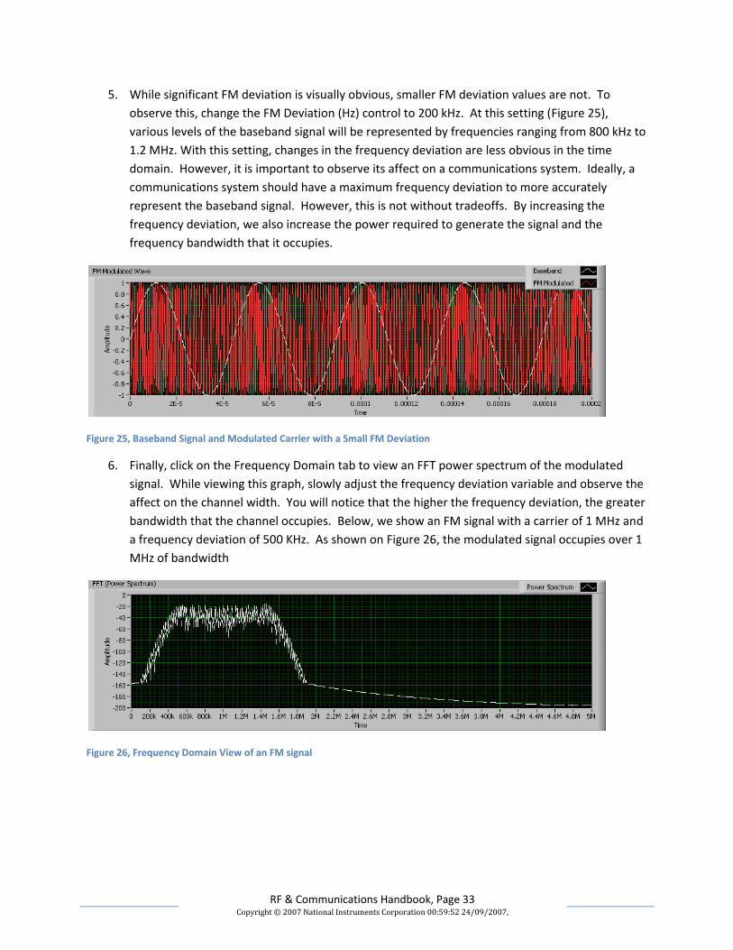
5. While significant FM deviation is visually obvious, smaller FM deviation values are not. To
observe this, change the FM Deviation (Hz) control to 200 kHz. At this setting (Figure 25),
various levels of the baseband signal will be represented by frequencies ranging from 800 kHz to
1.2 MHz. With this setting, changes in the frequency deviation are less obvious in the time
domain. However, it is important to observe its affect on a communications system. Ideally, a
communications system should have a maximum frequency deviation to more accurately
represent the baseband signal. However, this is not without tradeoffs. By increasing the
frequency deviation, we also increase the power required to generate the signal and the
frequency bandwidth that it occupies.
Figure 25, Baseband Signal and Modulated Carrier with a Small FM Deviation
6. Finally, click on the Frequency Domain tab to view an FFT power spectrum of the modulated
signal. While viewing this graph, slowly adjust the frequency deviation variable and observe the
affect on the channel width. You will notice that the higher the frequency deviation, the greater
bandwidth that the channel occupies. Below, we show an FM signal with a carrier of 1 MHz and
a frequency deviation of 500 KHz. As shown on Figure 26, the modulated signal occupies over 1
MHz of bandwidth
Figure 26, Frequency Domain View of an FM signal

RF & Communications Handbook, Page 34 Copyright © 2007 National Instruments Corporation 00:59:52 24/09/2007,
Phase Modulation (PM)
Phase Modulation encodes message signals as phase variations of the carrier signal. Phase modulation
and frequency modulation are closely related to each other. Although PM isn’t widely used for
transmission of analog signals, the concept of phase modulation is applicable to many popular digital
modulation schemes.
Background
In PM, the phase of the carrier signal is varied in proportion to the message signal. As we have seen in
the FM section, PM and FM are collectively referred to as Angle Modulation.
Given the carrier signal,
Equation 25
PM systems generate the modulated signal by varying the phase as,
Equation 26
where is the message signal and is the proportionality constant, known as phase deviation
constant.
PM is related to FM in that frequency is the rate of change of phase. As such, referring back to Figure 19,
we note that calculating an integral over the message signal with respect to time and then performing
PM modulation is equivalent to doing FM modulation on the original signal. Conversely, since frequency
is the rate of change of phase, and
Equation 27
we can implement PM by differentiating the message with respect to time and feeding this to the FM
modulator block.
PM demodulation involves finding the phase of the received signal. PM receiver design is more complex
compared to other analog modulation schemes (AM, FM) and consequently PM is not widely used.
PM Modulation Index
A PM Modulation Index can be defined as the maximum phase deviation of the modulated signal. More
formally,
Equation 28

RF & Communications Handbook, Page 35 Copyright © 2007 National Instruments Corporation 00:59:52 24/09/2007,
From Equation 26, the maximum phase deviation occurs when the message signal takes on the
maximum absolute value. Hence,
Equation 29
Conclusion
Phase Modulation (PM) encodes the message signal by varying the phase of the carrier signal and is
closely related to frequency modulation (FM). Even though phase modulation is not widely used for
transmitting analog signals, the concept is applicable to many popular digital modulation schemes.

RF & Communications Handbook, Page 36 Copyright © 2007 National Instruments Corporation 00:59:52 24/09/2007,
Digital Modulation
Digital modulation is a key concept that is fundamental to understanding modern communication
systems and their practical implementations. Wi-Fi, Bluetooth, CDMA, HDTV, XM radio are some
examples of communication systems that use digital modulation. With the commercial successes of
digital cameras, streaming-video applications, PDAs, laptops, computers and other computing devices, a
greater portion of data that we care about is digital. Digital data lends itself naturally to digital
modulation.
The term Digital Modulation is used when the data being modulated on the carrier is digital in nature.
Consequently, the modulation signal is limited to a finite (discrete) number of states. Contrast this with
analog modulation, where the data is analog and the modulation signal can take on an infinite number
of values. In both digital and analog modulation, the carrier is an analog signal.
Relative to analog modulation, digital modulation enables communication systems with:
More reliable communication
Higher data rates
Flexible hardware implementation
Integration of complex signal processing algorithms
This section discusses the theoretical background and some practical considerations related to digital
modulation techniques. We start with an introduction to the IQ representation of signals, and a
discussion of constellation symbols, which are key concepts in understanding digital modulation. Next,
we present the different digital modulation techniques prevalent in real-world systems and associated
step-by-step tutorials using National Instruments LabVIEW.
Introduction to IQ Signals
The in-phase (I) and quadrature-phase (Q) representation of signals is widely used in the context of
communication systems. As we will see in this section, this representation has a solid theoretical
foundation, but it is also practically useful in that it simplifies visualization and other common tasks
related to modulated signals.
Mathematical Background
Let’s look at how the IQ signal representation relates to the more traditional approach of representing
signals. The traditional approach represents the sine wave with the mathematical equation:
Equation 30

RF & Communications Handbook, Page 37 Copyright © 2007 National Instruments Corporation 00:59:52 24/09/2007,
In communication systems, the information to be transmitted is encoded by varying the parameters of a
carrier signal, typically a sine wave. As shown in Equation 30, the amplitude ( ), frequency ( ) and
phase ( ) are the three parameters that can be varied for modulating information on the carrier. In the
analog modulation section, we have seen some techniques for encoding information using these
parameters.
A visual representation of the sine wave using polar coordinate system is shown in Figure 27. Here, the
vector represents the instantaneous value of the sine wave. The magnitude of the vector (distance from
the origin) corresponds to the amplitude of the sine wave ( ) and the angle of the vector with respect
to the horizontal axis corresponds to the phase ( ) of the sine wave.
Figure 27, Polar representation of a sine wave
So far, we have seen how we can represent the instantaneous value of the sine wave with a vector. We
now take a look at how the frequency of the sine wave is related to this vector. Imagine the vector
rotating around the origin with a fixed magnitude. Because frequency is the rate of change of phase of
the signal, the speed at which the vector rotates about the origin gives us the frequency of the signal.
For example, a sine wave with a frequency of 1 Hz (2π radians/sec) will rotate counter-clockwise around
the origin at a rate of one revolution per second.
In-phase and Quadrature-phase components
Now that we understand the vector representation of a sine wave in the polar co-ordinate system,
understanding the IQ representation is straightforward. We simply consider the rectangular coordinates
of the instantaneous vector by switching from a polar coordinate system to a Cartesian (X,Y) coordinate
system. Figure 28 shows how the I and Q values relate to the magnitude and phase. The I and Q
components are projections of the vector on the horizontal (I-axis) and vertical (Q-axis) axes
respectively.

RF & Communications Handbook, Page 38 Copyright © 2007 National Instruments Corporation 00:59:52 24/09/2007,
Figure 28, Connecting I and Q with polar form representation of instantaneous state of sine wave
As we will see, digital modulation maps digital data to a set of points on the I-Q plane, or equivalently,
on the magnitude-phase plane. Switching from one point to another would change the phase,
magnitude, or both. Designing a flexible phase modulator in hardware is complex and so is building a
modulator that supports simultaneous magnitude and phase changes. This is where IQ representation
comes to the rescue. By changing only the amplitudes of the in-phase and quadrature-phase
components, we can effectively change the magnitude and phase of the carrier signal.
Let us now go back and express the traditional sine wave equation in terms of the in-phase and
quadrature-phase components. To do this, we will use the trigonometric identity
Equation 31
Setting and , it follows that
Equation 32
We denote the instantaneous amplitude of the carrier wave by . Multiplying the above equation
throughout by , we get
Equation 33
Plugging in the values for the IQ components, namely and
, we can rewrite the above equation as
Equation 34
This equation relates the IQ components to the traditional magnitude-angle representation. The left-
hand side (LHS) shows the modulated carrier signal with the message being encoded in the variations of

RF & Communications Handbook, Page 39 Copyright © 2007 National Instruments Corporation 00:59:52 24/09/2007,
the parameters ( ). The equivalent representation using IQ shows two sinusoidal signals of the
same frequency ( ) that differ by a phase of radians, the phase difference between and
. Signals with a phase difference of radians are said to be in-quadrature, and are
orthogonal. From a practical standpoint, this means that the I and Q components do not interfere with
each other and can be processed independently.
The IQ representation reduces the process of modulation to a few simple operations, namely,
manipulating the amplitudes of the I and Q components, multiplication with the carrier, and subtraction.
The simplicity of these operations greatly simplifies the hardware design, as we will see later in the
Advantages of using IQ section.

RF & Communications Handbook, Page 40 Copyright © 2007 National Instruments Corporation 00:59:52 24/09/2007,
The IQ Representation and Modulation
Let us leverage modulation concepts we learned in the analog modulation section to see how to
visualize modulation using the IQ representation of signals.
Figure 29, Time-domain representation of AM, FM, and PM Signals
Figure 29 shows various analog modulation techniques being applied to a carrier signal. In the AM case,
the message signal is the sine wave that forms the 'envelope' of the higher frequency carrier sine wave.
In the FM case, the message data is the dashed square wave. As the figure illustrates the resulting
carrier signal changes between two distinct frequency states. Each of these represents the high and low
state of the message signal. If the message signal were a sine wave in this case, there would be a more
gradual change in frequency much more difficult to see with the naked eye. In the PM case, notice the
abrupt phase change at the edges of the dashed square wave message signal.

RF & Communications Handbook, Page 41 Copyright © 2007 National Instruments Corporation 00:59:52 24/09/2007,
Let‘s consider what this looks like on the IQ plane. If only the amplitude of the carrier sine wave changes
with time and the phase and frequency stay constant (AM), we should see a vector with fixed phase
whose distance from the origin varies. In the IQ plane, only the I data will change with time. This is
evidenced by the following image (Figure 30):
Figure 30, Visualization of AM: Time-domain waveform for the sinusoidal message signal and IQ representation of the modulated signal, captured at 3 different time instants. The IQ representation shows a vector with one end fixed at the origin, the length of the vector representing the I value.
The amplitude of the in-phase component tracks changes in the sinusoid message signal. At T=t0, the
sinusoid is at its maximum amplitude and so is the I-component. Then the sinusoid amplitude starts
decreasing causing a decrease in the I-signal also. At T=t1, when the message signal amplitude reaches
its minimum value, the I-component also takes on the minimum value. Finally, the third snapshot with
T=t2 shows the zero-crossing point of the sinusoid. As expected, the I-component amplitude is also mid-
way between its minimum and maximum values.
T=t0 T=t1 T = t2

RF & Communications Handbook, Page 42 Copyright © 2007 National Instruments Corporation 00:59:52 24/09/2007,
Now considering PM modulation, the carrier phase changes with time and the amplitude and frequency
stay constant. Therefore, we expect to see changes in the IQ plane only with respect to the angle of the
modulated signal with respect to the origin. This is evidenced by Figure 31:
Figure 31, Visualization of PM: Time-domain waveform for the sinusoidal message signal and IQ representation of the modulated signal, captured at 3 different time instants. The IQ representation shows a vector with one end fixed at the origin. The projection of the vector on I and Q axis represents the I and Q values respectively.
In PM, the phase of the modulated signal tracks changes in the message signal. Here, the phase takes on
values between and radians. At T=t0, when the sinusoid is at its peak amplitude, the phase
of the vector is maximum ( ). Here I=0 and Q takes on its maximum value (Q=1). Then the
sinusoid amplitude decreases causing the vector to rotate clock-wise (i.e. phase or angle with respect to
the origin decreases). At T=t1, the phase reaches ( ) with the message signal taking on its
minimum amplitude. Note that I=0 again and Q takes on its minimum value (Q=-1). Next, the message
signal amplitude increases causing the vector to rotate counter-clockwise (i.e. phase increases). The
snapshot at T=t3 shows the zero-crossing point of the message. As expected, the phase is mid-way
between its minimum and maximum values (i.e. ). Note that Q=0 and the I-component is at its
maximum value (I=1). Finally, the signal returns to its peak amplitude and radians again. The
periodic nature of the message signal results in this pattern of rotation being repeated. Finally, we note
that at points between the three states shown (T=t1, T=t2, T=t3), both the I and Q components will be
non-zero.
T=t0 T=t1 T = t2

RF & Communications Handbook, Page 43 Copyright © 2007 National Instruments Corporation 00:59:52 24/09/2007,
FM is a little more difficult to visualize using instantaneous vector representation. Recall that in FM, the
frequency of the modulated signal changes in proportion to the message signal. Therefore, just like the
PM modulation case, we expect to see a vector with constant magnitude rotating about the origin.
However, the rotation rate will now vary based on the frequency that is selected. Figure 32 shows the
vector rotating in a circle with the dotted line representing the modulated signal amplitude. We expect
the rate of rotation (frequency) of the modulated signal to track the changes in the message signal.
Figure 32, The vector representation of a modulated signal. For an FM modulated signal, the vector of fixed amplitude rotates about the origin with the rate of rotation tracking changes in the message signal.
Advantages of using IQ
Using in-phase and quadrature-phase components to represent signals greatly simplifies the analog
circuitry used in RF communication systems. An analog hardware implementation of a signal modulator
that directly manipulates the magnitude and phase of a carrier sine wave can be expensive and difficult
to build. Precisely varying the phase of a high frequency carrier sine wave based on an input message
signal, also called direct phase manipulation, is difficult and complex to achieve in an analog circuit.
By using the IQ representation, we can build simple circuits for modulation and avoid having to
manipulate the phase of an RF carrier directly. Recall that the modulated carrier signal can be written in
terms of its IQ components as:
Equation 35
I
Q
Amplitude

RF & Communications Handbook, Page 44 Copyright © 2007 National Instruments Corporation 00:59:52 24/09/2007,
Hence, we can control the amplitude and phase of the RF carrier sine wave by simply manipulating only
the amplitudes of the I and Q signals! This eliminates the need for a direct phase modulator and greatly
simplifies the task of simultaneous amplitude and phase modulation. The hardware components
required for implementing modulation are reduced to a local oscillator, a constant phase shifter, two
mixers and an adder circuit. Figure 33 gives the block diagram for implementing modulation using IQ
signals. The block is sometimes referred to as an IQ modulator.
Figure 33, Upconversion of baseband IQ data to RF using an IQ Modulator
Let’s now consider how practical systems implement modulation using the IQ representation. The block
diagram of a transmitter that uses IQ signals is shown in Figure 33. It shows the technique of quadrature
upconversion, a method widely used in practical communication systems.
The system takes the baseband data represented by IQ components as input and produces the RF
modulated carrier. Because the I and Q components are orthogonal, they can be processed
independently. The local oscillator generates the carrier signal with a frequency . The phase shifter
generates a 90 degrees phase-shifted version of the carrier. The I and Q data are multiplied with their
respective carrier signals using the two mixers. Finally, the RF output signal is generated by subtracting
the quadrature-phase carrier signal from the in-phase carrier signal.
The quadrature modulator shown in Figure 33 can be used for any modulation scheme. This is because
the IQ modulator is merely reacting to changes in I and Q waveform amplitudes, and I and Q data can be
used to represent any changes in magnitude and phase of a message signal. The flexibility and simplicity
of this design is the fundamental reason for its widespread use and popularity.
We conclude our discussion with a summary of some of the benefits of using the IQ representation in
communication systems:
Eliminates direct phase manipulation circuitry
Flexible hardware - one circuitry supports all modulation schemes
Mapping Bits to Symbols
In digital modulation, the number of bits sent per second is called Bit Rate - the higher the bit rate, the
faster the communication speed. One way for digital communication systems to support a higher bit
rate is to encode multiple bits of information in the variations of the carrier signal.

RF & Communications Handbook, Page 45 Copyright © 2007 National Instruments Corporation 00:59:52 24/09/2007,
The simplest digital modulation, binary amplitude shift keying (binary ASK), encodes information in the
amplitude variations of the signal. At any given moment, the amplitude can be set to one of two states,
corresponding to a digit ‘0’ or digit ‘1’. Other binary modulation schemes such as binary phase shift
keying and binary frequency shift keying, also represent bits directly.
In M-ary modulation, there are M possible states the modulating signal can take. The states are
commonly referred to as symbols, with each symbol representing bits of information. Thus,
binary modulation schemes (M=2) use two symbols to transmit data, each representing a single bit,
while Quad-ary schemes (M=4) use four symbols with each symbol representing two bits. Figure 34
illustrates one way 4-ASK modulation can represent bits.
Figure 34, Amplitude shift keying with M=4. There are 4 states the modulated signal amplitude can take.
As mentioned previously, the IQ representation of signals helps in the implementation and visualization
of modulation. Consequently, symbols are typically expressed using the IQ representation. The
relationship between the symbols and their corresponding IQ values is depicted using a “symbol map“.
Figure 35 below shows a symbol map for 4-ASK modulation and quadrature phase shift keying
modulation with M=4 (4-PSK). Each symbol corresponds to a unique point on the IQ plane. Note that
the ASK modulated signal always has zero for the quadrature-component since the phase of the
modulated signal never changes. For 4-PSK, differences between unique symbols will correspond to
both I and Q data changes. Also note that the 4-PSK symbols are equidistant from the origin implying a
fixed amplitude for the modulated signal.
Figure 35, Symbol maps for 4-ASK modulation (left) and 4-PSK modulation (right)
00 01
A = 0 A = 1
11 10
Amplitude (A)
I 00 01 11 10
Q
I
Q
00
01 11
10

RF & Communications Handbook, Page 46 Copyright © 2007 National Instruments Corporation 00:59:52 24/09/2007,
Bits, Symbols, and Rate
It is useful to note the relationship between bit rate and the rate for symbol transmission, the Symbol
Rate. For binary (M=2) modulation schemes, the symbol rate equals the bit rate. Both 4-ASK and 4-PSK
transmit bits of information per channel use (i.e. per transmission). For M=16, the modulated
signal will have 16 possible states and would transmit 4 bits of information per channel use.
For a given symbol rate with an M-ary modulation scheme, the corresponding bit rate would be
times the symbol rate. This relationship means that for a fixed symbol rate, using a modulation scheme
with an increased M-ary (e.g. starting with 2-ASK and moving to 4-ASK) shows the potential of increasing
the bit rate. However, increasing M corresponds to a decreasing distance between symbols making it
harder at the receiver to distinguish between adjacent symbols. Consequently, most practical systems
today limit themselves to M=2, ..., 64.
As we have discussed, any modulation scheme can be implemented using an IQ modulator. With an IQ
modulator, the process would involve:
1. Mapping groups of bits to symbols (i.e. to a unique IQ value) based on the digital modulation
technique chosen.
2. Using an IQ modulator to generate the modulated signal based on the IQ value.
The IQ modulator samples (reads) the IQ values periodically. The time duration between two
consecutive reads is called the symbol clock period and the inverse of the symbol clock period is the
symbol rate.

RF & Communications Handbook, Page 47 Copyright © 2007 National Instruments Corporation 00:59:52 24/09/2007,
Types of Digital Modulation
Amplitude Shift Keying (ASK)
Amplitude Shift Keying is a form of digital modulation that encodes the data by changing the amplitude
of the carrier signal. Each ASK symbol maps to a unique amplitude level. Common applications for ASK
include low-cost communication systems such as remote controls, toys, remote keyless entry systems
for automobiles, and wireless .sensors and other applications where cost and/or hardware complexity
are of concern.
Figure 36, Time domain representation of 2-ASK modulated signal and the bit-pattern being transmitted. Digit ‘0’ is mapped to a signal amplitude of zero.
Background
ASK is the digital version of the analog AM (amplitude modulation) scheme. In contrast to AM, ASK uses
a finite (discrete) number of amplitude levels. For instance, in 2-ASK the carrier amplitude ( ) can take
on one of two possible values. Figure 36 shows an example time-domain waveform of a 2-ASK
modulated output. Since the receiver relies on signal amplitude for reliably decoding the data, ASK is
sensitive to amplitude changes caused by the communication channel and can be prone to errors.
ASK modulated signals do not have a constant envelope, i.e. the amplitude of the modulated carrier
wave varies. Although this characteristic can simplify the design of an ASK receiver, it typically reduces
the power efficiency of the transmitter.
ASK Symbol Mapping
The number of amplitude levels dictates the number of bits per symbol. On-off keying (OOK), for
example, is a 2-level (binary) ASK modulation scheme - digit ‘0’ corresponds to an amplitude level of
zero (off) for a specific duration, and a ‘1’ corresponds to the maximum amplitude for that duration.
Figure 37 shows symbol maps for the OOK and 4-ASK.

RF & Communications Handbook, Page 48 Copyright © 2007 National Instruments Corporation 00:59:52 24/09/2007,
Figure 37, Several constellations for amplitude shift keying - 2-ASK or OOK (left), 4-ASK (right)
In 4-ASK, one of four amplitude levels is selected for the carrier signal based on the data to be
modulated. We note that an ASK modulated signal always has zero for the quadrature-component.
Conclusion
Amplitude Shift Keying is a simple digital modulation scheme amenable to low-cost implementation
using simple hardware. ASK finds widespread use in commercial applications like X10, RFID, remote
keyless entry, and telemetry applications.

RF & Communications Handbook, Page 49 Copyright © 2007 National Instruments Corporation 00:59:52 24/09/2007,
Frequency Shift Keying (FSK)
Frequency Shift Keying encodes digital data by varying the frequency of the carrier signal.
Communication systems that use FSK include RFID, cordless phones, remote controls and the GSM
mobile phone standard.
Figure 38, Time domain signal of 2-FSK transmission. The data being transmitting is 1-1-1-0-1-0, starting at time t=9E-7 (i.e. the first half of the transmitted signal for the first bit is not shown here).
Background
Frequency Shift Keying is the digital counterpart of frequency modulation (FM). In FSK the frequency
modulated signal transitions between a set of discrete frequencies based on the data to be transmitted.
Figure 38 shows a 2-FSK modulated signal. We note that the same signal would be generated if an
analog pulse signal was transmitted using FM.
In FSK, the spacing between the frequencies that the carrier can take is an important system parameter.
It is desirable to minimize this spacing in order to increase the bandwidth efficiency of the system. To
avoid interference between the different frequencies, a minimum spacing of half the carrier period is
required between the frequency values.
FSK Symbol Mapping
Depending on the constellation size, each symbol can represent 1, 2, 4, or more bits. In an FSK
transmission with 1 bit per symbol, two frequencies are used – one frequency representing a digit ‘0’,
the other frequency a digit ‘1’. This is called 2-FSK. 4-FSK uses 4 different frequency values with 2 bits
per symbol. The frequency of a signal is not easily viewed on I/Q plots. Instead, we illustrate FSK
modulation using the frequency-domain representation of the modulated signal. Figure 39 below shows
the frequency-domain representation for 2-FSK and 4-FSK.

RF & Communications Handbook, Page 50 Copyright © 2007 National Instruments Corporation 00:59:52 24/09/2007,
Figure 39, Frequency domain signal of a 2-FSK transmission (left) and 4-FSK (right)
Variations of FSK
A variation of FSK with a higher spectral efficiency is Minimum Shift Keying (MSK). In MSK, two
frequencies are used (2-FSK) where the separation between the two frequencies is half the bit rate. This
results in the waveforms representing digit ‘0‘ and digital ‘1’ to differ by exactly one-half of the carrier
period. This is the minimum spacing needed to avoid any interference between the signals, and thus the
name Minimum Shift Keying. The high spectral efficiency makes MSK an attractive modulation scheme
for practical implementations.
Conclusion
Frequency Shift Keying is a straightforward, important digital modulation scheme and is used in a variety
of applications ranging from RFIDs, GSM mobile phone standard, to cordless phones and tire pressure
sensors.
Frequency Shift Keying Tutorial
In this FSK tutorial, we will build a VI to perform M-ary FSK modulation and study the effect of symbol
rate, constellation size, and frequency spacing on the modulated signal.
1. Open FSK_Transceiver(template).vi and switch to the block diagram (Figure 40). Several
controls, constants, and indicators have already been created and organized for ease of
programming. There is also a while loop allowing the FSK simulation to run continuously until
the user hits the Stop button. All the code for this example will be inside the loop.
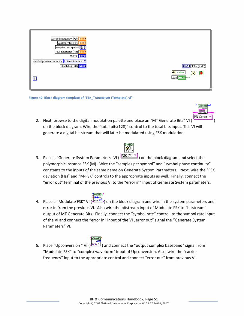
RF & Communications Handbook, Page 51 Copyright © 2007 National Instruments Corporation 00:59:52 24/09/2007,
Figure 40, Block diagram template of “FSK_Transceiver (Template).vi”
2. Next, browse to the digital modulation palette and place an “MT Generate Bits” VI ( )
on the block diagram. Wire the “total bits(128)” control to the total bits input. This VI will
generate a digital bit stream that will later be modulated using FSK modulation.
3. Place a “Generate System Parameters” VI ( ) on the block diagram and select the
polymorphic instance FSK (M). Wire the “samples per symbol” and “symbol phase continuity”
constants to the inputs of the same name on Generate System Parameters. Next, wire the “FSK
deviation (Hz)” and “M-FSK” controls to the appropriate inputs as well. Finally, connect the
“error out” terminal of the previous VI to the “error in” input of Generate System parameters.
4. Place a “Modulate FSK” VI ( ) on the block diagram and wire in the system parameters and
error in from the previous VI. Also wire the bitstream input of Modulate FSK to “bitstream”
output of MT Generate Bits. Finally, connect the “symbol rate“ control to the symbol rate input
of the VI and connect the “error in“ input of the VI „error out“ signal the “Generate System
Parameters“ VI.
5. Place “Upconversion ” VI ( ) and connect the “output complex baseband“ signal from
“Modulate FSK“ to “complex waveform“ input of Upconversion. Also, wire the “carrier
frequency” input to the appropriate control and connect “error out“ from previous VI.
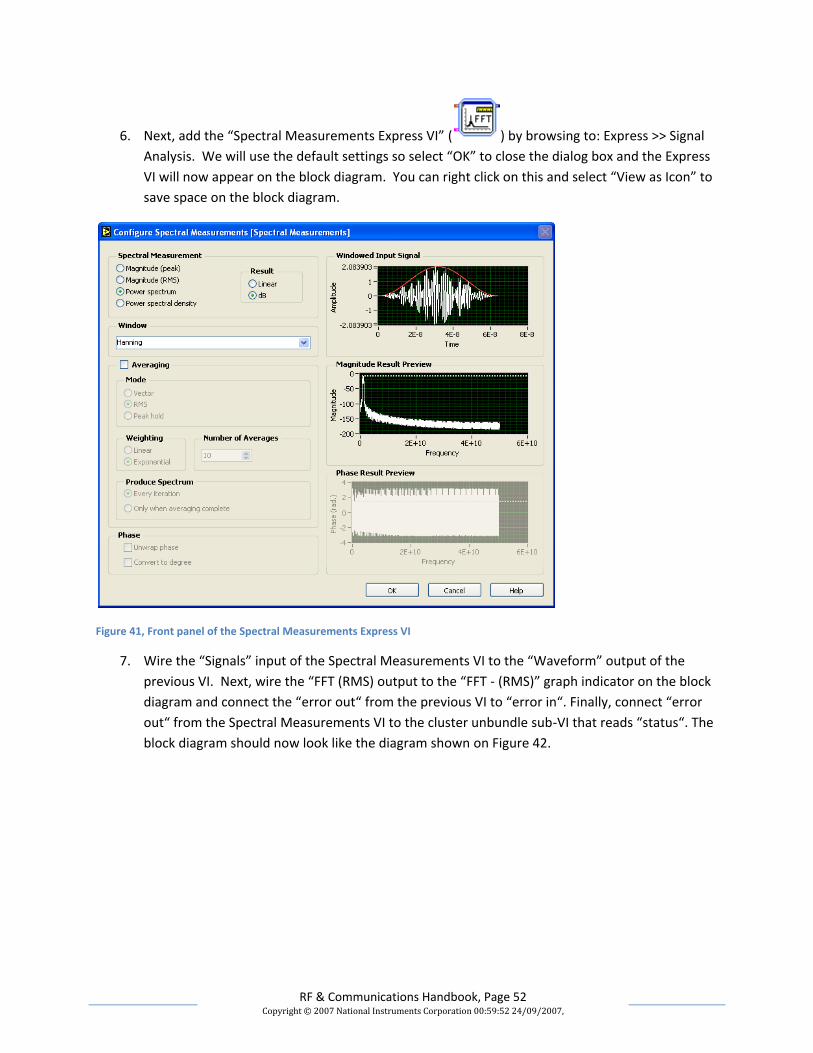
RF & Communications Handbook, Page 52 Copyright © 2007 National Instruments Corporation 00:59:52 24/09/2007,
6. Next, add the “Spectral Measurements Express VI” ( ) by browsing to: Express >> Signal
Analysis. We will use the default settings so select “OK” to close the dialog box and the Express
VI will now appear on the block diagram. You can right click on this and select “View as Icon” to
save space on the block diagram.
Figure 41, Front panel of the Spectral Measurements Express VI
7. Wire the “Signals” input of the Spectral Measurements VI to the “Waveform” output of the
previous VI. Next, wire the “FFT (RMS) output to the “FFT - (RMS)” graph indicator on the block
diagram and connect the “error out“ from the previous VI to “error in“. Finally, connect “error
out“ from the Spectral Measurements VI to the cluster unbundle sub-VI that reads “status“. The
block diagram should now look like the diagram shown on Figure 42.

RF & Communications Handbook, Page 53 Copyright © 2007 National Instruments Corporation 00:59:52 24/09/2007,
Figure 42, Block diagram of FSK_Transceiver(Completed).vi
FSK Demonstration
Next, we will examine various parameters of an FSK transmitter and observe their effects on the
spectrum of the modulated signal. Most notably, we will change characteristics such as: M-ary, deviation
frequency, and symbol rate to observe the effects upon the frequency domain of the signal.
First, click on the LabVIEW run button to begin executing the program just created. Note in the FFT-
(RMS) graph that the signal power is centered at 5 MHz, the carrier frequency. In addition, four peaks
are visible and they are spaced by approximately 650 MHz. The location of these peaks corresponds to
the four frequencies being used in transition. Note that “4” has been selected in the “M-FSK” control.
This is referred to as the M-ary of the modulation scheme and indicates that data is transmitted by
adjusting the frequency so that it is one of 4 values.
Figure 43, A 4-FSK transmission

RF & Communications Handbook, Page 54 Copyright © 2007 National Instruments Corporation 00:59:52 24/09/2007,
Next, we will explore the affect of M-ary on the frequency domain. Adjust the M-FSK control to all
possible values (2, 4, 8) and observe the affect in the frequency domain. As you can see, the number of
peaks corresponds to the number of frequencies chosen for the M-ary. You will notice that when M-FSK
= 8, that that each of the peaks interfere with one another making it difficult to distinguish between
them. This occurs because the frequencies are not appropriately spaced. This issue is addressed in the
next step.
Figure 44, Differences in the spectrum of a 2-FSK (left) and 4-FSK (right)
FSK deviation determines the spacing of each of these peaks. More specifically, it signifies the
difference, in frequency, between the carrier frequency and the outermost frequency band. So far, we
have used 1 MHz for this value. However, when 8-MSK is chosen, the bandwidth of each channel is too
wide for all the channels to fit in the selected frequency deviation. We can change the FSK deviation (Hz)
control to accommodate more channels. Experiment with this value and observe the results in the
frequency domain. Below, we show the frequency spectrum with frequency deviations of 1.25 MHz and
3 MHz.
Figure 45, 8-FSk with 1.25MHz frequency deviation (left) and 3MHz frequency deviation (right)

RF & Communications Handbook, Page 55 Copyright © 2007 National Instruments Corporation 00:59:52 24/09/2007,
Phase Shift Keying (PSK)
Phase Shift Keying encodes data by changing the phase of the carrier signal. A unique phase shift is
selected for each symbol. Offset PSK (OPSK) and differential PSK (DSPK) are two widely used variants of
PSK. Communication systems that leverage PSK include Wi-Fi, Zigbee, RFID, and deep space telemetry.
Background
PSK encodes symbols as discrete phase variations ( ) of the carrier signal. For example, 2-level PSK, also
called binary phase shift keying (BPSK), maps a digit ’0‘ to 0 phase and digit ‘1‘to a phase of 180 . In
contrast to amplitude-shift keying (ASK), PSK signals have a constant envelope, i.e. the carrier amplitude
( ) is the same for all symbols making PSK less susceptible than ASK to amplitude variations.
PSK Symbol Mapping
Figure 46 shows the symbol maps for PSK modulation with constellation sizes of 2, 4 and 8. Binary Phase
Shift Keying (BPSK) transmits one bit per symbol and is one of the simplest digital modulation
techniques. 4-PSK, popularly known as quadrature phase shift keying (QPSK), transmits 2 bits per symbol
while 8-PSK transmits 3 bits per symbol. As we have discussed earlier, larger constellations support
higher data rates but the trade-off is the increase in the probability of incorrect detection at the
receiver.
Figure 46, PSK Implementations: M=2, BPSK (left), M =4, QPSK (middle), M=8, 8-PSK (right)
PSK Variations
Differential PSK (DPSK) and Offset Quadrature PSK (OQPSK) are two interesting variants of PSK which
can simplify system implementation.
DPSK encodes the data in the relative phase shift between consecutive symbols. For instance, in
differential BPSK, a digit ’0’ results in the carrier phase unchanged and a digit ‘1‘ corresponds to a phase
shift of 180 with respect to the previous value of carrier phase. Demodulation occurs by comparing the
phase of the received signal with that of the previous symbol. As a self-referencing scheme, DPSK
eliminates the need for a reference signal in the demodulator.
In OQPSK, the quadrature component of the signal is delayed by half a cycle. This causes the In-phase
component (I) and quadrature-phase component (Q) to never transition at the same time. Figure 47
shows the phase trajectories of non-Offset QPSK and Offset QPSK. The biggest benefit of OQPSK is that
the IQ data never transitions through the origin, which represents zero amplitude and would require an
amplifier to switch-off and back on again which can inject a lot of noise into the transmitted signal.
Linear amplifiers, typically the amplifier of choice for RF systems, are only linear over a finite range of

RF & Communications Handbook, Page 56 Copyright © 2007 National Instruments Corporation 00:59:52 24/09/2007,
amplitudes and if it’s possible to decrease the fluctuation of the signal, we can better suit the amplifier
to our application, which can also take less power, making it ideally suited for low power applications
like Zigbee and RFID.
Figure 47, Difference between non-Offset QPSK and offset QPSK. Offset QPSK never transitions through the origin, where non-Offset QPSK does.
Conclusion
Phase Shift Keying is an important digital modulation scheme because of its simplicity and widespread
use in commercial applications. Example applications that use PSK modulation include Wi-Fi, Zigbee,
RFID, deep space telemetry and cell phones.
Non-offset PSK Offset PSK

RF & Communications Handbook, Page 57 Copyright © 2007 National Instruments Corporation 00:59:52 24/09/2007,
Phase Shift Keying Tutorial
In this PSK tutorial, we will construct a LabVIEW VI that transmits and receives a digital bit stream in
software using PSK modulation.
Background
Figure 48 shows a constellation plot that shows the symbol map for 8-PSK. Here each of the 8 symbols
or constellation points represents 3-bits of digital data. Here the raw IQ data is shown as the red
‘yarnball‘ and the white dots represent the IQ data at the instants when they are sampled (read) by the
symbol clock. Notice that all of the symbols are at the same amplitude (equidistant from the origin), and
it is the phase that differentiates them. Also notice that the each symbol is equally spaced in phase
across the unit circle.
Figure 48, Constellation plot for 8-PSK modulation
Programming
1. Open “PSK_Transceiver(Template)” VI and inspect the front panel that has already been
constructed (Figure 49). When this VI is completed, it will allow the user to choose the number
of symbols that will be used (M-ary PSK) and study the effect of noise on the modulation.
000
001
100
101 111
110
010
011

RF & Communications Handbook, Page 58 Copyright © 2007 National Instruments Corporation 00:59:52 24/09/2007,
Figure 49, Front panel of PSK_Transceiver(Template).vi
2. Examine the block diagram for the VI. It consists of a while loop that will iterate once every 100
milliseconds. Inside this loop, we will generate, modulate, demodulate and display digital data.
Figure 50, Block diagram template of PSK_Transceiver(Template).vi
3. Place a “Generate System Parameters” VI ( ) on the block diagram and select the
polymorphic instance PSK (M). Connect the wire coming from the M-PSK control to the
corresponding input terminal on this VI. This VI will create a PSK symbol map based on the M-
ary value selected on the front panel.
4. Place an “MT Bit Generation” VI ( ) on the block diagram and wire the output of the
multiplication function to the total bits input. This VI will generate a digital bit stream that will

RF & Communications Handbook, Page 59 Copyright © 2007 National Instruments Corporation 00:59:52 24/09/2007,
later be modulated using PSK. The default for this VI is to generate pseudo-random bit sequence
of the specified number of bits.
5. Place a “Generate Filter Coefficients” VI ( ) on the block diagram. Right click on the
modulation type terminal and create a constant, then select PSK. Wire the pulse shaping filter
control into the appropriate input. This VI will generate filter coefficients that will be used
during modulation to reduce the bandwidth of the modulated signal.
6. Place a “Modulate PSK” VI ( ) on the block diagram and wire in the system parameters, bit
stream, and pulse shaping coefficients from the three previous VIs. Also wire the Boolean value
from the first call function into the reset? input. This VI will perform PSK modulation on the
input bit stream using the system parameters and filter coefficients specified.
7. Place an “Add AWGN” VI ( ) on the block diagram and wire the Noise Impairments control
to the Eb/N0 input. Also wire the Boolean value from the first call function into the reset? input.
This VI will subject the IQ waveform to Additive White Gaussian Noise based on the “Eb/N0”
control on the front panel and enables the user to test the robustness of the system against a
noisy channel. A value of Eb/N0 = 0 means noise power equals signal power. As “Eb/N0”
increases, the ratio of signal power to noise power increases exponentially and we can expect
the system performance to improve significantly.
8. Place a “Demodulate PSK” VI ( ) on the block diagram and wire the system parameters,
filter coefficients and input complex waveform form previous VIs. Also wire the Boolean value
from the first call function into the reset? input. This VI will demodulate the input signal and
return the recovered bit stream.
9. Place a “Format Constellation Graph” VI ( ) and connect the waveform input to the
corresponding output from the “Demodulate PSK” VI. Connect the constellation reference input
to the reference named XYGraph. This VI prepares the signal for visualization as a constellation
diagram.
10. Finally, wire the error out of each VI to the error in of the next to handle any errors that occur
and enforce dataflow between the VIs. Connect the loop tunnel for error out to the Error

RF & Communications Handbook, Page 60 Copyright © 2007 National Instruments Corporation 00:59:52 24/09/2007,
Handler outside the loop. Switch to the front panel and run the VI to see PSK modulation in
action. Experiment with the constellation size (M), and Eb/N0. Using a very large amount of
simulated noise will cause the demodulation quality to degrade, eventually leading to extremely
poor receiver performance.
Figure 51, Block diagram of PSK_Transceiver(Completed).vi
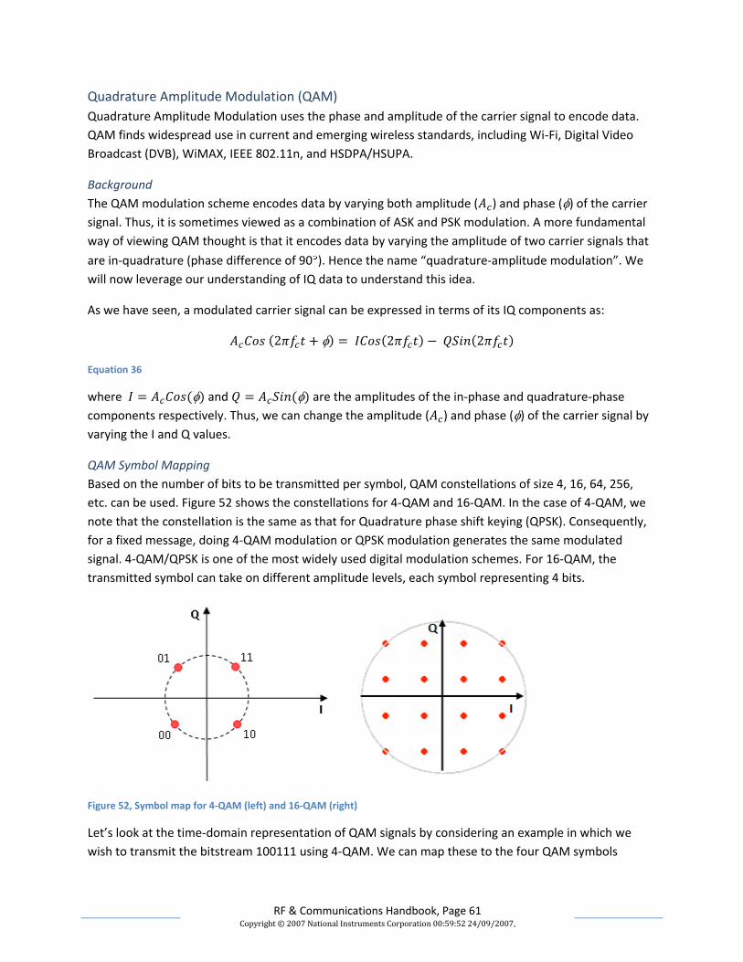
RF & Communications Handbook, Page 61 Copyright © 2007 National Instruments Corporation 00:59:52 24/09/2007,
Quadrature Amplitude Modulation (QAM)
Quadrature Amplitude Modulation uses the phase and amplitude of the carrier signal to encode data.
QAM finds widespread use in current and emerging wireless standards, including Wi-Fi, Digital Video
Broadcast (DVB), WiMAX, IEEE 802.11n, and HSDPA/HSUPA.
Background
The QAM modulation scheme encodes data by varying both amplitude ( ) and phase ( ) of the carrier
signal. Thus, it is sometimes viewed as a combination of ASK and PSK modulation. A more fundamental
way of viewing QAM thought is that it encodes data by varying the amplitude of two carrier signals that
are in-quadrature (phase difference of 90 ). Hence the name “quadrature-amplitude modulation”. We
will now leverage our understanding of IQ data to understand this idea.
As we have seen, a modulated carrier signal can be expressed in terms of its IQ components as:
Equation 36
where and are the amplitudes of the in-phase and quadrature-phase
components respectively. Thus, we can change the amplitude ( ) and phase ( ) of the carrier signal by
varying the I and Q values.
QAM Symbol Mapping
Based on the number of bits to be transmitted per symbol, QAM constellations of size 4, 16, 64, 256,
etc. can be used. Figure 52 shows the constellations for 4-QAM and 16-QAM. In the case of 4-QAM, we
note that the constellation is the same as that for Quadrature phase shift keying (QPSK). Consequently,
for a fixed message, doing 4-QAM modulation or QPSK modulation generates the same modulated
signal. 4-QAM/QPSK is one of the most widely used digital modulation schemes. For 16-QAM, the
transmitted symbol can take on different amplitude levels, each symbol representing 4 bits.
Figure 52, Symbol map for 4-QAM (left) and 16-QAM (right)
Let’s look at the time-domain representation of QAM signals by considering an example in which we
wish to transmit the bitstream 100111 using 4-QAM. We can map these to the four QAM symbols

RF & Communications Handbook, Page 62 Copyright © 2007 National Instruments Corporation 00:59:52 24/09/2007,
representing 10, 01, 11. Figure 53 shows the time-domain waveform that results for this bitstream. Each
symbol is represented by one period of the sine wave and has a unique phase shift. In this respect, 4-
QAM might be considered a special case of QAM where the amplitude is the same for all symbols.
Figure 53, Time domain representation of a 4-QAM modulation. From left to right, the signals represent the bit patterns 10, 01, and 11
The constellation plot in Figure 54 shows the phase and amplitude transitions of the carrier signal. The
raw IQ data is represented by the red trance with the white dots representing those samples of IQ data
that occur on symbol clock periods and that are mapped back to digital bit patterns based on the 4-QAM
symbol map. We note that the transitions go through the origin. This causes abrupt amplitude variations
between consecutive symbols and causes noise to be injected in the transmitted symbol due to the
amplifier turning off and back on abruptly. This problem can be fixed by using offset-QAM. Refer to the
offset-PSK modulation scheme discussed earlier for more details.
Figure 54, Constellation plot of a 4-QAM (identical to QPSK) modulation
Conclusion
Quadrature Amplitude Modulation is an important modulation scheme with many practical applications,
including current and future wireless technologies. Some examples of communication systems that use
QAM are Wi-Fi, cable modems, Digital Video Broadcast (DVB), and WiMAX.
A

RF & Communications Handbook, Page 63 Copyright © 2007 National Instruments Corporation 00:59:52 24/09/2007,
Quadrature Amplitude Modulation (QAM) Tutorial
This tutorial examines QAM modulation, demonstrating the relationship between digital message bit
patterns, symbols, QAM constellation points, I/Q values and time-domain signals.
1. Open the VI entitled QAMSymbolMapTutorial.vi, and click on the run button in LabVIEW to
begin execution.
2. Examine the top of the VI front panel (Figure 55). It consists of a row of green digital buttons the
user can click on to toggle between values of 0 and 1. This bit sequence represents the digital bit
pattern to be QAM modulated. Because we are using 16-QAM modulation, this bit stream is
grouped into 4 bit chunks, or symbols, where each one of the 16-QAM constellation points
represents one of the possible sixteen bit patterns that can be represented by four binary digits
( ).
Figure 55, Custom bitstream in QAMSymbolMapTutorial.vi
3. Look directly below the bit stream portion of the front panel (Figure 56) to find the images
showing a 16-QAM constellation plot. There are three separate images because the twelve
digital bits are grouped into three separate symbols, and each one of these constellation plots
graphs one of these symbols as a solid red dot. For example, the first symbol 1111 maps to the
point -0.236 + 0.707i in the IQ plane, which again is simply the Cartesian representation of a
particular magnitude / phase combination. The I axis is the horizontal axis and the Q axis is the
vertical axis.
Figure 56, Representation of the symbols in polar representation
4. Spend some time manipulating the digital bit pattern and see the effects upon the particular
constellation points the bit pattern maps to. If two symbols represent the same four-bit pattern,
they will have the same I and Q coordinates (they will map to the same constellation point).

RF & Communications Handbook, Page 64 Copyright © 2007 National Instruments Corporation 00:59:52 24/09/2007,
5. Look near the bottom of the front panel to find three graphs of sine waves representing the IQ
coordinates (i.e. with the magnitude and phase described by the Cartesian IQ points). Notice
how symbols / constellation points farther from the origin will have larger amplitude.
6. We should also observe the relationship between the digital bit pattern and the actual carrier
waveform. Click on the initial bit pattern array to change the symbols that are being generated.
In this case, we have chosen a carrier frequency that is equal to the symbol rate. Thus, the
phase and amplitude of our carrier represents a new symbol at the rate of exactly one symbol
per period. In the graph indicator (Figure 57), we have labeled the first three periods of our
carrier signal to correspond with the first three symbols of the IQ waveform. Now, as we modify
our bitstream, we see the IQ waveform also change as well. We can see from the resulting
waveform below that each symbol produces a different phase and amplitude in the time domain
of the carrier signal.
Figure 57, Generated waveforms corresponding to symbols

RF & Communications Handbook, Page 65 Copyright © 2007 National Instruments Corporation 00:59:52 24/09/2007,
7. Next, let us evaluate how changes in the symbol map correspond to a different signal in the time
domain. To start with, choose the bit pattern: 001101100111. As we can see on the front panel
(Figure 58), this pattern is grouped into 0011, 0110, 0111. In addition, we can see on our polar
graph that each of the symbols being generated represent the maximum amplitude (1) of our
carrier waveform.
Figure 58, Example for a bit pattern and the corresponding polar representation (note that each of the symbols being generated represents the maximum amplitude of our carrier waveform)
8. Next, we will choose a bit pattern that produces a signal that is smaller in amplitude. To do this,
enter the bit pattern of: 100111001101. Again, this bitstream is broken into 4-bit groupings to
produce: 1001, 1100, 1101. Observe the new symbols on the polar graph, which are also shown
below:
Figure 59, polar representation of the bit pattern: 100111001101
9. As we can see from the polar representation above, the phase of the three new symbols has not
changed. However, the amplitude of the three new symbols is smaller than the original set.
Thus, we can see this effect in the resulting waveform, which has the same phase as the original.
To observe this affect, enter several different bitstreams to observe the changes in the phase

RF & Communications Handbook, Page 66 Copyright © 2007 National Instruments Corporation 00:59:52 24/09/2007,
and amplitude of the upconverted waveform. A key characteristic to observe is that each set of
four bits affect only the first symbol of the waveform.
Figure 60, Resulting waveform of the bit pattern: 100111001101

RF & Communications Handbook, Page 67 Copyright © 2007 National Instruments Corporation 00:59:52 24/09/2007,
Hardware Labs
Introduction to PXI Hardware
This section introduces the PXI platform and discusses how it relates to National Instruments RF
Hardware. The topics in this section include:
1. Overview and Background on PXI
2. PXI Features, Technologies and Benchmarks
3. Introduction to the National Instruments RF and Communications Platform
4. Overview of RF VSA, VSG, CW, Switching and Preamp
Figure 61, Instrumentation Timeline
To understand the history of instrumentation architectures, let us examine a timeline depicting the
introduction of several popular instrument architectures. In 1965, the General Purpose Interface Bus
(GPIB) was developed to interface with popular bench-top instruments. In 1987, VXI (which stands for
VME eXtensions for Instrumentation) was introduced, ushering in the era of modular-based
instruments. In the early 90’s, PC plug-in instruments were developed to take advantage of the popular
PCI bus found on standard desktop PC’s. Then, in 1995, CompactPCI built on PC technology by
introducing a rugged, modular architecture, thus paving the way for the introduction of PXI in 1997.
Overview and Background on PXI
PXI, the fastest growing instrumentation architecture over the last decade, was officially established in
1998 through an alliance of instrument, control and automation vendors. These member companies
formed the PXI Systems Alliance (PXISA) whose goals are to maintain and improve the PXI specification,
ensure device interoperability as well as to promote the PXI standard.
GPIB
1965
VXI
1987
CompactPCI
1995
PXI
1997

RF & Communications Handbook, Page 68 Copyright © 2007 National Instruments Corporation 00:59:52 24/09/2007,
Figure 62, PXI beginnings
Currently, there are over 68 members in the PXISA. Through these members and other organizations,
close to 1200 different devices have been released for PXI. For more information, visit the PXISA website
at http://www.pxisa.org for specifications, tutorials, applications notes, whitepapers, and to locate
member companies and products.
Figure 63, PXI background information
PXI stands for PCI eXtensions for Instrumentation. PXI, which also takes advantage of the performance
of the PCI bus, utilizes the same rugged Eurocard design as CompactPCI, is completely compatible with
CompactPCI modules, but adds an extra connector for advanced timing and triggering. This timing and
triggering bus, as we will later see, allows users to trigger and synchronize multiple instruments in the
same system; thus improving overall performance.
The PXI form factor is relatively small in size – about the same height as a standard PC plug in card.
Standard 3u modules (such as the modules shown here) have a height of 100 mm, or approximately 4
inches.
PXI = PCI eXtensions for Instrumentation
CompactPCI Eurocard design with added timing and triggering capabilities
cPCI PXI
PCI Bus
PCI Bus
Timing and
Triggering
Bus 100 mm
~4 inches
gfsdgsdfg
0
200
400
600
800
1000
1200
1998 2000 2002 2004
Number of Modules
PXI Systems Alliance
Founded in 1998
Goals
Maintain the PXI specification
Ensure interoperability
Promote the PXI standard
Currently 68+ members comprise PXISA
Visit the PXISA Website (www.pxisa.org) for
o Specifications
o Tutorials, Application Notes, and White Papers
o Locate member companies and products

RF & Communications Handbook, Page 69 Copyright © 2007 National Instruments Corporation 00:59:52 24/09/2007,
Figure 64, PXI system components
The chassis provides the rugged and modular packaging for the system. It regulates the cooling and
power distribution to each slot and chassis generally range in size from 4- to 18-slots, and also are
available with special features such as DC power supplies and integrated signal conditioning. The chassis
contains the high-performance PXI backplane, which includes the PCI bus and timing and triggering
buses. These timing and triggering buses enable users to develop systems for applications requiring
precise synchronization. For more information on the functionality of the PXI timing and triggering
buses, refer to the PXI Hardware Specification at www.pxisa.org/specs.htm.
As defined by the PXI Hardware Specification, all PXI chassis contain a system controller slot located in
the leftmost slot of the chassis (slot 1). Controller options include remote control from a standard
desktop PC or a high-performance embedded control with either a Microsoft operating system (such as
Windows 2000/XP/Vista) or a Real-Time operating system (such as LabVIEW Real-Time). Windows-based
controllers have same look and feel as Windows-based desktop PCs. These controllers are offered with
high performance processors (such as a Intel Core-Duo), and the entire controller resides embedded in a
slot of the PXI chassis. NI also offers a line of controllers that only operate with the RTOS and use
compactFlash drives. These controllers are designed for applications requiring deterministic and reliable
performance and are run under headless operation (i.e. no mouse, keyboard).
PXI Features, Technologies and Benchmarks
PXI is widely adopted with close to 1200 PXI modules offered to fulfill various measurement
applications. PXI also integrates easily with instrumentation system such as GPIB, Serial, and/or VXI. PXI
PXI Backplane
PCI bus synchronization
Peripheral Slots
PXI Controller
Embedded PC, real-time
controller or remote PC
interface
Runs standard software
Chassis
AC or DC
Power defined per slot
Cooling defined per slot
Bus Extension
GPIB, VXI, PXI extension,
Ethernet, serial, parallel, etc.

RF & Communications Handbook, Page 70 Copyright © 2007 National Instruments Corporation 00:59:52 24/09/2007,
offer seamless integration with these architectures. Then, as time progresses, PXI allows you to expand
your system to keep up with current technology and meet your evolving test and measurement needs.
Figure 65, Key PXI features
PXI is modular. This means that you, the user, “buy only what you need”. The instrument vendor
does not define the make-up of your system – you do!!
PXI is “a PC” in a ruggedized box. Thus, if you can operate a standard desktop PC, you already
know how to operate a PXI system.
PXI offers advanced timing and synchronization, as we will see in our demo in a few moments.
And, most importantly, PXI takes advantage of standard technology.
The major strength of PXI is that it uses proven, industry-standard technology. PXI is built on
CompactPCI, an industrial version of the PCI bus found in almost all desktop computers. PXI then adds
timing, triggering, and synchronization similar to the functionality delivered in VXI.
For easy integration, PXI uses OS, driver, and networking standards from the PC software market,
including plug and play drivers. Because PXI and CompactPCI offer complete interoperability, users can
use any core CompactPCI product in a PXI system and vice-versa.

RF & Communications Handbook, Page 71 Copyright © 2007 National Instruments Corporation 00:59:52 24/09/2007,
Figure 66, Integrating Multiple Platforms – Hybrid Systems
All of these existing instrumentation systems easily integrate into a PXI based system. PXI systems are
controlled with either an embedded controller or a MXI interface card interfaced to a desktop. The
image above has an embedded controller but it could be a MXI interface card as well. This is done
through Ethernet, or MXI-4 to integrate Desktop PCs. Also there are GPIB ports on many embedded
controllers, you can use MXI-2 to integrate with VXI architectures, and PXI is compatible with
CompactPCI cards.
With all of these interfaces to existing equipment, PXI as an instrumentation platform preserves your
existing investment.
In addition to offering an overall large number of PXI modules, PXI system providers also offer a wide
range of modules. Some of the alternatives include:
DAQ AND CONTROL:
Multifunction I/O
Reconfigurable I/O
Digital I/O
Analog Input / Output
Vision and Motion
Counter/Timers
Desktop PC
MXI-2
VXI GPIB/Serial
CompactPCI
Ethernet
(or MXI)
INSTRUMENTS:
Oscilloscopes
Digital Waveform
Generator/Analyzers
Digital Multimeters
Signal Generators
Switching
RF Signal Generation and
Analysis
INTERFACES:
GPIB
SCSI + Enet
Boundary Scan/JTAG
CAN + DeviceNET
RS-232/RS-485
VXI/VME

RF & Communications Handbook, Page 72 Copyright © 2007 National Instruments Corporation 00:59:52 24/09/2007,
Figure 67, Digitizer performance benchmarks
Many high-speed digitizers and oscilloscopes have common measurement functions such as voltage
amplitude, rise time, and overshoot built into the driver or firmware. PC-based digitizers can take
advantage of the latest PC processor technology to perform these measurements up to 300 times faster
than popular standalone oscilloscopes. Measurement speed will continue to increase as processor
technology advances, whereas it is not possible to upgrade the processor in traditional box
instrumentation. These benchmarks include the time for each device to perform the requested
measurement and return the single value to the host PC, configuration time is not included. In this case,
the GPIB bus is not the limiting factor, because we use the oscilloscope’s onboard processor to compute
the measurement and transfer only a single data point across the bus.
On the other hand, when you need to perform any unique analysis on the acquired waveform, the
speed of a PC based digitizer over a box oscilloscope becomes important. Unique analysis includes those
measurements that are not built into the driver such as frequency response, breakdown voltage, time of
fly, and others. The increased throughput performance is due to the fact that high-speed digitizers use
the 132 MB/s PCI bus to transfer data to the PC processor to perform your custom analysis routines,
whereas most GPIB instruments have transfer rates of only 1 MB/s.
0 50 100 150 200 250 300 350 400 450
Overshoot
Rise Time
Amplitude
Measurements per second
NI 5122 High-Speed Digitizer Traditional Oscilloscope #1 Traditional Oscilloscope #2

RF & Communications Handbook, Page 73 Copyright © 2007 National Instruments Corporation 00:59:52 24/09/2007,
Figure 68, Performance Benchmarks – NI PXI-5660 2.7-GHz RF Signal Analyzer
Let’s look at a benchmark that illustrates the throughput advantages of the entire RF signal analyzer as
compared to traditional instrumentation. This benchmark shows a comparison in making power-in-band
measurements at several different frequency spans. Here, we see the powerful combination of the real-
time bandwidth of the downconverter with the digitizer and the advantages of running the NI optimized
FFT algorithms on the latest commercial processors. When making measurements like power-in-band,
the RF signal analyzer delivers measurement throughput advantages of 30 to 200 times over traditional
instrumentation.
Introduction to the National Instruments RF and Communications Platform
One approach to keeping stride with RF and wireless advances in test is through software, where
engineers model new channel coding and modulation techniques or algorithms. The logical solution is
to take a software-defined approach to instrumentation by using coding and modulation software to
generate and measure signals through modular, general-purpose RF instruments. This software-defined
approach to test is then completely application-driven and user-defined.
Figure 69, The NI RF & Communications Platform uses a modular, software-defined approach to RF & microwave.
0 0.5 1 1.5 2 2.5 3 3.5 4 4.5
160 kHz
320 kHz
800 kHz
Fre
qu
ency
Sp
an
Measurements per second
Traditional Instrumentation NI RFSA

RF & Communications Handbook, Page 74 Copyright © 2007 National Instruments Corporation 00:59:52 24/09/2007,
Overview of RF VSA, VSG, CW, Switching and Preamp Modules
The National Instruments PXI-565x RF and microwave signal generator is continuous-wave with
modulation capability. In a single 3U PXI slot, the NI PXI-565x signal generator provides exceptional
phase noise and signal jitter. With the PXI-565x 6.6-GHz RF and microwave signal generator, you can
easily set up sophisticated stimulus response or tracking generator applications using the NI PXI-5660 RF
vector signal analyzer and the National Instruments LabVIEW graphical development environment.
Figure 70, RF Signal Generators & Analyzers
The National Instruments PXI-5671 module is a 3-slot RF vector signal generator that delivers signal
generation from 250 kHz to 2.7 GHz, 20 MHz of real-time bandwidth and up to 512 MB of memory. The
onboard quadrature digital upconverter significantly extends waveform playback time and reduces the
time required to compute and download waveform data by computing the waveform data using the
onboard field programmable gate array (FPGA). This functionality is ideal for engineers who require data
streaming with rapid response time for software-defined radio (SDR) or faster download times for
satellite radio applications. In addition, the NI PXI-5671 can generate custom and standard modulation
formats including AM, FM, PM, ASK, FSK, MSK, GMSK, PSK, QPSK, PAM, and QAM.
The National Instruments PXI-5660 is a modular 2.7-GHz RF vector signal analyzer optimized for
automated test. It provides high-throughput RF measurements in a compact, 3U PXI package. The NI
PXI-5660 features a wide real-time bandwidth, a highly stable timebase, and flexible software tools that
can handle measurement applications ranging from component characterization in R&D to the remote
monitoring of RF navigation systems deployed in the field.
The National Instruments RF switch modules are ideal for expanding the channel count or increasing the
flexibility of systems with signal bandwidths greater than 10 MHz. Available PXI and SCXI switch module
configurations include high-density multiplexers, dimensionally flexible sparse matrices, and general-
purpose relays. NI has optimized each of these modules for minimal insertion loss, reflection, and
crosstalk and maximum isolation between channels. Here is a short list of the different modules
available.
1) Multiplexer
a) PXI-2593 16x1 500 MHz
b) PXI-2592 4x1 2.5 GHz
c) PXI-2595 4x1 5 GHz

RF & Communications Handbook, Page 75 Copyright © 2007 National Instruments Corporation 00:59:52 24/09/2007,
d) PXI-2596 Dual 6x1 26.5 GHz
e) PXI-2597 6x1 Terminated 26.5 GHz
2) General-Purpose Relays
a) PXI-2598 Dual Transfer Switch 26.5 GHz
b) PXI-2599 Dual SPDT 26.5 GHz
3) Matrix
a) PXI-2593 18-terminal sparse matrix 500 MHz
Figure 71, PXI-based switch & preamplifier modules
The National Instruments RF (radio frequency) switch modules are ideal for expanding the channel
count or increasing the flexibility of systems with signal bandwidths greater than 10 MHz. Available PXI
and SCXI switch module configurations include high-density multiplexers, dimensionally flexible sparse
matrices, and general-purpose relays. NI has optimized each of these modules for minimal insertion loss,
reflection, and crosstalk and maximum isolation between channels.
RF & Communications Test Development Software
Sometimes too much flexibility can imply more development time. For example, if I wanted to develop
and test an RFID device or a wireless sensor and I needed to modulated and demodulate ASK and FSK, I
would not want to start writing code to modulate and demodulate these formats. Or if I was using an RF
signal analyzer to do spectral monitoring and I needed to demodulate many different modulation
formats, it could be a daunting task writing code for this application.

RF & Communications Handbook, Page 76 Copyright © 2007 National Instruments Corporation 00:59:52 24/09/2007,
Figure 72, Screen captures from displays generated in LabVIEW with the Modulation Toolkit and the Spectral Measurements Toolkit
National Instruments ships the Modulation Toolkit with every vector signal generator that allows all the
standard modulation formats to be generated, even custom formats. This way, the code is already
written for the standard formats – then you can build on top of these basic building blocks.
The National Instruments Modulation Toolkit extends the built-in analysis capability of LabVIEW with
functions and tools for signal generation, analysis, visualization, and processing of standard and custom
digital and analog modulation formats. With this toolkit, you can rapidly develop custom applications for
research, design, characterization, validation, and test of communications systems and components that
modulate or demodulate signals. Applications for the NI Modulation Toolkit are numerous; they include
digital modulation formats (AM, FM, PM, ASK, FSK, MSK, GMSK, PSK, QPSK, PAM, and QAM) that are the
foundation of many digital communication standards found in 802.11a/b/g/n, ZigBee (802.15.4), WiMAX
(802.16), RFID, satellite communications, and commercial broadcast among others.
For RF signals and spectrum analysis, National Instruments provides the Spectral Measurements Toolkit.
The Spectral Measurements Toolkit provides a set of flexible spectral measurements in LabVIEW and
LabWindows/CVI, including power spectrum, peak power and frequency, in-band power, adjacent-
channel power, and occupied bandwidth, as well as 3D spectrogram capabilities. In addition, the
Spectral Measurements Toolkit contains VIs and functions for performing modulation-domain
operations such as passband (IF) to baseband (I-Q) conversion, I-Q to IF conversion, and
generation/analysis of analog modulated signals. The combination of these optimized algorithms and
the GHz processing of your PC delivers unmatched measurement throughput.
Summary
PXI eases system integration with close to 1200 modules leveraging standard technology and integration
with existing GPIB, Serial and VIX systems. PXI is the most advanced test, measurement and automation
platform including advanced timing and synchronization with expandability to PXI Express. NI RF &
Communications platform uses a modular, software-defined approach to RF & microwave test to solve
multiple applications and communication standards.
Additional Resources
www.pxisa.org
www.ni.com/pxi

RF & Communications Handbook, Page 77 Copyright © 2007 National Instruments Corporation 00:59:52 24/09/2007,
Hardware Configuration
This section describes how to configure National Instruments RF hardware. The topics covered include:
A description of Measurement & Automation Explorer (MAX)
How to configure the NI PXI-5661 Vector Signal Analyzer
How to configure the NI PXI-567x Vector Signal Generator
How to use Test Panels to generate sine tones (567x) and acquire a spectrum (5661)
Figure 73, The NI PXI-5661 consists of two PXI modules, the NI PXI-5600 and the NI PXI-5142.
The NI PXI-5661 RF Vector Signal Analyzer consists of the two PXI hardware modules:
NI PXI-5600 – 2.7 GHz RF superheterodyne downconverter module with output frequencies
between 5 and 25 MHz.
NI PXI-5142 – 14 bit, 100 megasample-per-second (MS/s) digitizer module.
Configuring the NI PXI-5660
When using the NI PXI-5660 instead of the NI PXI-5661, there is a different procedure for device setup
because the NI PXI-5660 is built on the Traditional NI-DAQ hardware driver. These devices will appear
under the Traditional NI-DAQ (Legacy) Devices section of MAX. When running example programs from
LabVIEW, reference the downconverter device number and digitizer resource name in order to control
the NI PXI-5660 hardware.
PXI-5600 PXI-5142

RF & Communications Handbook, Page 78 Copyright © 2007 National Instruments Corporation 00:59:52 24/09/2007,
Figure 74, NI PXI-567x consists of two PXI modules, the NI PXI-5610 and either a NI PXI-5421 or a NI PXI-5441.
The NI PXI-567x RF Vector Signal Analyzer consists of the following two PXI hardware modules:
NI PXI-5610 – 2.7 GHz RF superheterodyne upconverter module with input frequencies between
15 and 35 MHz.
One of the following arbitrary waveform generator (AWG) modules:
o NI PXI-5421 – 16 bit, 100 megasample-per-second (MS/s) AWG module
o NI PXI-5441 – 16 bit, 100 megasample-per-second (MS/s) AWG module with digital
upconversion (DUC) capability
PXI-5610 PXI-54xx

RF & Communications Handbook, Page 79 Copyright © 2007 National Instruments Corporation 00:59:52 24/09/2007,
Figure 75, Measurement & Automation Explorer (MAX)
The Windows Configuration Manager keeps track of all the hardware installed in your computer,
including National Instruments RF devices. If you have a Plug & Play (PnP) device, the Windows
Configuration Manager automatically detects and configures the device. All National Instruments RF
devices are Plug & Play (PnP).
You can verify the Windows Configuration by accessing the Device Manager, available by selecting
Start»Settings»Control Panel»System»Device Manager. You can see Data Acquisition Devices, which lists
all RF devices installed in your computer. Double-click a RF device to display a dialog box with tabbed
pages. The General tab displays overall information regarding the device. The Resources tab specifies
the system resources to the device such as interrupt levels, DMA, and base address for software-
configurable devices. The NI-DAQ Information tab specifies the bus type of the RF device. The Driver tab
specifies the driver version and location for the RF device.
Configuration using Measurement & Automation Explorer
NI-RFSG and NI-RFSA install Measurement & Automation Explorer (MAX), a software utility that
establishes all device and channel configuration parameters. After installing an RF device in your
computer, you must run this configuration utility. MAX reads the information the Device Manager
records in the Windows Registry and assigns a logical device number to each RF device. Use the device
number to refer to the device in LabVIEW.
5661 567x

RF & Communications Handbook, Page 80 Copyright © 2007 National Instruments Corporation 00:59:52 24/09/2007,
You can access MAX either by
Double-clicking its icon on the desktop or
Selecting Tools»Measurement & Automation Explorer in LabVIEW.
Figure 76, You can right-click on a module name in MAX and select Rename to rename a module.
MAX allows you to rename any DAQmx hardware module. The MAX name is used in software
(LabVIEW, LabWindows/CVI, C) to operate the module’s hardware resources. You do not have to
change the modules names from the default, but doing so can make programming easier.
To rename a PXI module, right-click the device in MAX and select Rename from the shortcut menu.
Enter the new name that you would like to associate with the module. Click OK.
Figure 77, MAX: Configuration of PXI-5661
The NI PXI-5661 RF Vector Signal Analyzer consists of the following two PXI hardware modules:

RF & Communications Handbook, Page 81 Copyright © 2007 National Instruments Corporation 00:59:52 24/09/2007,
NI PXI-5600 – 2.7 GHz RF superheterodyne downconverter module with output frequencies
between 5 and 25 MHz.
NI PXI-5142 – 14 bit, 100 megasample-per-second (MS/s) digitizer module
You must create a MAX association between the NI 5600 downconverter module and the NI 5142
digitizer module to control both hardware modules as a single RF signal analyzer. Right-click on the NI
PXI-5600 and select Properties from the pull-down menu. In the Device Properties dialog box select the
NI 5142 Digitizer that is connected to the NI 5600. Once this is done select OK and the devices are now
configured as an NI PXI-5661 Vector Signal Analyzer.
Figure 78, MAX: Configuration of PXI-567x
The NI PXI-567x RF Vector Signal Analyzer consists of the following two PXI hardware modules:
NI PXI-5610 – 2.7 GHz RF superheterodyne upconverter module with input frequencies between
15 and 35 MHz.
And one of the following arbitrary waveform generator (AWG) modules:
o NI PXI-5421 – 16 bit, 100 megasample-per-second (MS/s) AWG module
o NI PXI-5441 – 16 bit, 100 megasample-per-second (MS/s) AWG module with digital
upconversion (DUC) capability
You must create a MAX association between the NI 5610 upconverter module and the NI 54xx AWG
module to control both hardware modules as a single RF signal generator. Right-click on the NI PXI-5600
and select Properties from the pull-down menu. In the Device Properties dialog box select the NI 54xx
AWG module that is connected to the NI 5600. Once this is done select OK and the devices are now
configured as an NI PXI-567x Vector Signal Generator.
Note: The NI PXI-565x RF Signal Generator and NI PXI-5690 Preamplifier are single-slot PXI modules and
do not need any configuration in MAX. As long as they show up under NI-DAQmx Devices in MAX they
will operate correctly.

RF & Communications Handbook, Page 82 Copyright © 2007 National Instruments Corporation 00:59:52 24/09/2007,
Figure 79, Test-Panels: Acquisition with the PXI-5661
To verify the device configuration, use the NI-RFSA test panel in MAX to acquire a spectrum using the RF
signal analyzer hardware. The NI-RFSA test panel tests both NI 5661 hardware modules as a single
instrument. To access the test panel, right-click the NI PXI-5600 downconverter module and select Test
Panels. In the NI PXI-5661 tab of the Test Panels dialog box, specify a center frequency, reference level,
span, and resolution bandwidth (RBW). Click Start to begin signal acquisition and view the acquired data
in the Power Spectrum plot.
Figure 80, Test-Panels: Generation with the PXI-567x
To verify the device configuration, use the NI-RFSG test panel in MAX to generate a simple signal using
the RF signal generator hardware. The NI-RFSG test panel tests both NI 567x hardware modules as a
single instrument. To access the test panel, right-click the NI PXI-5610 upconverter module and select
Test Panels. In the NI PXI-567x tab of the Test Panels dialog box, specify a frequency and a power level

RF & Communications Handbook, Page 83 Copyright © 2007 National Instruments Corporation 00:59:52 24/09/2007,
for signal generation. Click Start to begin signal generation. During signal generation the ACTIVE LEDs
on both NI 567x hardware modules are activated.
The test panel for the NI PXI-565x RF Signal Generator can be accessed using the same steps listed above
and looks almost identical to the test panel for the PXI-567x.

RF & Communications Handbook, Page 84 Copyright © 2007 National Instruments Corporation 00:59:52 24/09/2007,
Index
Adjacent Channel Power (ACP), 11
Amplitude Modulation (AM), 17
Amplitude Shift Keying (ASK), 47
Angle Modulation, 34
Binary Phase Shift Keying (BPSK), 55
Bit Rate, 44
Differential PSK (DPSK), 55
Digital Modulation, 36
Double Sideband AM Modulation, 19
Dynamic Range, 10
Fast Fourier Transform (FFT), 8
Frequency Modulation (FM), 26
Frequency Shift Keying (FSK), 49
Harmonic Distortion, 13
Minimum Shift Keying (MSK), 50
Modulation, 15
Modulation Index (AM), 18
Modulation Index (FM), 29
Modulation Index (PM), 34
Noise Floor, 9
Occupied Bandwidth, 11
Offset Quadrature PSK (OQPSK), 55
Phase Modulation (PM), 34
Phase Shift Keying (PSK), 55
Power in Band, 10
Quadrature Amplitude Modulation (QAM), 61
Resolution Bandwidth (RBW), 8
Signal to Noise Ratio (SNR), 10
Single Sideband AM Modulation, 19
Spurious Free Dynamic Range (SFDR), 10
Suppressed Carrier AM Modulation, 19
Symbol Rate, 46