rf basics i and ii - arxiv · rf basics i and ii frank gerigk cern, geneva, switzerland abstract...
TRANSCRIPT

RF Basics I and II
Frank GerigkCERN, Geneva, Switzerland
AbstractMaxwell’s equations are introduced in their general form, together with a basicset of mathematical operations needed to work with them. After simplifyingand adapting the equations for application to radio frequency problems, wederive the most important formulae and characteristic quantities for cavitiesand waveguides. Several practical examples are given to demonstrate the useof the derived equations and to explain the importance of the most commonfigures of merit.
1 Introduction to Maxwell’s equations1.1 Maxwell’s equationsMaxwell’s equations were published in their earliest form in 1861–1862 in a paper entitled “On physi-cal lines of force” by the Scottish physicist and mathematician James Clerk Maxwell. They represent auniquely complete set of equations that covers all areas of electrostatic and magnetostatic problems, aswell as electrodynamic problems, of which radio frequency (RF) engineering is only a subset. Surpris-ingly, they include the effects of relativity even though they were conceived much earlier than Einstein’stheories.
In differential form, Maxwell’s equations can be written as
∇×H = J+∂D∂ t
, (1)
∇×E =−∂B∂ t
, Maxwell’s equations (2)
∇ ·D = qv , (3)
∇ ·B = 0 , (4)
where the field components and constants are defined as follows:
E , electric field (V/m)
D = ε0εrE , dielectric displacement (A s/m2) (5)
B , magnetic induction, magnetic flux density (T)
H =1
µ0µrB , magnetic field strength or field intensity (A/m) (6)
J = κE , electric current density (A/m2) (7)ddt
D , displacement current (A/m2)
ε0 = 8.854 ·10−12 , electric field constant (F/m) (8)
εr , relative dielectric constant
µ0 = 4π ·10−7 , magnetic field constant (H/m) (9)
µr , relative permeability constantκ . electrical conductivity (S/m)
arX
iv:1
302.
5264
v1 [
phys
ics.
acc-
ph]
21
Feb
2013
In the following sections, we shall see that most of the important RF formulae can be derived in afew lines from Maxwell’s equations.
1.2 Basic vector analysis and its application to Maxwell’s equationsIn order to make efficient use of Maxwell’s equations, some basic vector analysis is needed, which isintroduced in this section. More detailed introductions can be found in a number of textbooks, such asfor instance the excellent Feynman Lectures on Physics [1].
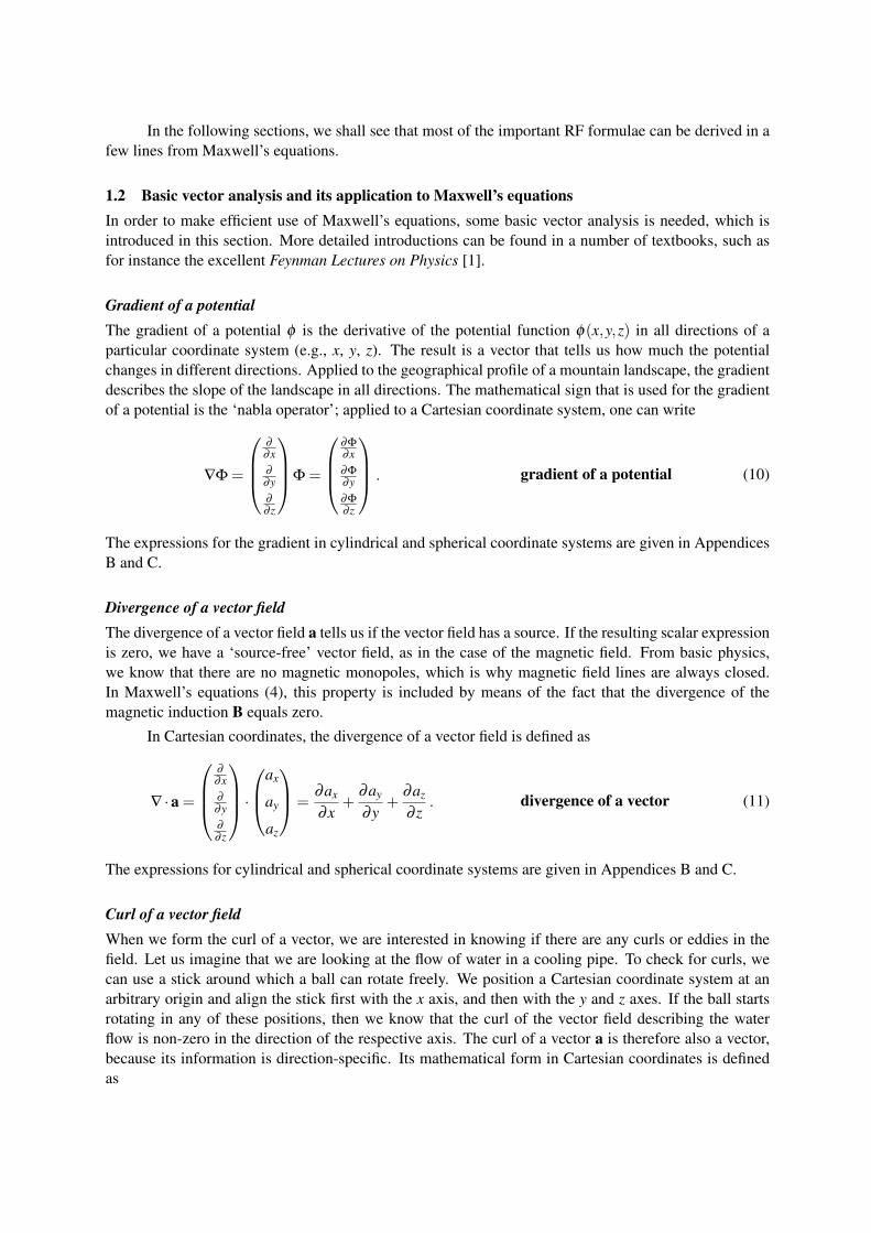
Gradient of a potentialThe gradient of a potential φ is the derivative of the potential function φ(x,y,z) in all directions of aparticular coordinate system (e.g., x, y, z). The result is a vector that tells us how much the potentialchanges in different directions. Applied to the geographical profile of a mountain landscape, the gradientdescribes the slope of the landscape in all directions. The mathematical sign that is used for the gradientof a potential is the ‘nabla operator’; applied to a Cartesian coordinate system, one can write
∇Φ =
∂
∂x∂
∂y∂
∂ z
Φ =
∂Φ
∂x∂Φ
∂y∂Φ
∂ z
. gradient of a potential (10)
The expressions for the gradient in cylindrical and spherical coordinate systems are given in AppendicesB and C.
Divergence of a vector fieldThe divergence of a vector field a tells us if the vector field has a source. If the resulting scalar expressionis zero, we have a ‘source-free’ vector field, as in the case of the magnetic field. From basic physics,we know that there are no magnetic monopoles, which is why magnetic field lines are always closed.In Maxwell’s equations (4), this property is included by means of the fact that the divergence of themagnetic induction B equals zero.
In Cartesian coordinates, the divergence of a vector field is defined as
∇ ·a =
∂
∂x∂
∂y∂
∂ z
·ax
ay
az
=∂ax
∂x+
∂ay
∂y+
∂az
∂ z. divergence of a vector (11)
The expressions for cylindrical and spherical coordinate systems are given in Appendices B and C.
Curl of a vector fieldWhen we form the curl of a vector, we are interested in knowing if there are any curls or eddies in thefield. Let us imagine that we are looking at the flow of water in a cooling pipe. To check for curls, wecan use a stick around which a ball can rotate freely. We position a Cartesian coordinate system at anarbitrary origin and align the stick first with the x axis, and then with the y and z axes. If the ball startsrotating in any of these positions, then we know that the curl of the vector field describing the waterflow is non-zero in the direction of the respective axis. The curl of a vector a is therefore also a vector,because its information is direction-specific. Its mathematical form in Cartesian coordinates is definedas

∇×a =
∂
∂x∂
∂y∂
∂ z
×ax
ay
az
= det
ux uy uz
∂
∂x∂
∂y∂
∂ z
ax ay az
=
∂az∂y −
∂ay∂ z
∂ax∂ z −
∂az∂x
∂ay∂x −
∂ax∂y
.
curl of a vector (12)
The unit vectors un have no physical meaning and simply point in the x, y, and z directions. They havea constant length of 1. The expressions for cylindrical and spherical coordinate systems can be found inAppendices B and C.
Second derivativesIn some instances, we have to make use of second derivatives. One of the expressions that is usedregularly in electrodynamics is the Laplace operator ∆ = ∇2, which—since the operator itself is scalar—can be applied to both scalar fields and vector fields:
∆φ = ∇ · (∇φ) = ∇2φ =
∂ 2φ
∂x2 +∂ 2φ
∂y2 +∂ 2φ
∂ z2 . Laplace operator (13)
The expressions for cylindrical and spherical coordinate systems can be found in Appendices B and C.
We also introduce two interesting identities:
∇× (∇φ) = 0 , (14)
∇ · (∇×a) = 0 . (15)
Equation (14) tells us that if the curl of a vector equals zero, then this vector can be written as thegradient of a potential. This feature can save us a lot of writing when we are dealing with complicatedthree-dimensional expressions for electric and magnetic fields, and we shall use this principle later onto define non-physical potential functions that can describe (via derivatives) complete three-dimensionalvector functions.
In the same way, Eq. (15) can (and will) be used to describe divergence-free fields with simple‘vector potentials’.
1.3 Useful theorems by Gauss and StokesThe theorems of Gauss and Stokes are some of the most commonly used transformations in this chapter,and therefore we shall take a moment to explain the concepts of them.
Gauss’s theoremGauss’s theorem not only saves us a lot of mathematics but also has a very useful physical interpretationwhen applied to Maxwell’s equations. Mathematically speaking, we transform a volume integral overthe divergence of a vector into a surface integral over the vector itself:∫
V
∇ ·a︸︷︷︸‘sources’
dV =
C∮S
a ·dS . Gauss’s theorem (16)

The surface on the right-hand side of the theorem is the one that surrounds the volume on the left-handside. If we remember that the divergence of a vector field is equal to its sources, Gauss’s theorem tellsus that:
– The vector flux through a closed surface equals the sources of flux within the enclosed volume.– If there are no sources, the amounts of flux entering and leaving the volume must be equal.
These statements can be applied directly to Maxwell’s equations. Using Eq. (3) and applyingGauss’s theorem, we obtain ∫
V
∇ ·EdV =∮S
E ·dS =Qε
(17)
(Fig. 1), which means that one can calculate the amount of charge in a volume simply by integrating theelectric flux lines over any closed surface that surrounds the charge, or vice versa.
Fig. 1: Example of electric flux lines emanating from electric charge in the centre of a sphere
The same trick can be applied to the source-free magnetic field. Here, we use Eq. (4) and obtain∫V
∇ ·BdV =∮S
B ·dS = 0 . (18)
Equation (18) gives us the proof of what was already stated earlier: magnetic field lines have no sources(∇ ·B = 0), and therefore the magnetic flux lines are always closed and have neither sources nor sinks.If magnetic flux lines enter a volume, then they also have to leave that volume (Fig. 2).
Fig. 2: Example of magnetic flux lines penetrating a sphere
Stokes’s theoremWhereas Gauss’s theorem is useful for equations involving the divergence of a vector, Stokes’s theoremoffers a similar simplification for equations that contain the curl of a vector. With Stokes’s theorem, wecan transform surface integrals over the curl of a vector into closed line integrals over the vector itself:∫
A
(∇×a) ·dA =
C∮C
a ·dl . Stokes’s theorem (19)
One can interpret Stokes’s theorem with the help of Fig. 3 as follows:

– the area integral over the curl of a vector field can be calculated from a line integral along its closedborders, or
– the field lines of a vector field with non-zero curl must be closed contours.
Fig. 3: Illustration of Stokes’s theorem
The meaning of these statements becomes immediately clear when we apply Stokes’s theorem toMaxwell’s equation (1): ∫
A
(∇×H) ·dA =∮C
H ·dl =∫A
(J+
dDdt
)·dA . (20)
In the electrostatic case, the time derivative disappears and the area integral over the current density may,for instance, be the current flowing in an electric wire as shown in Fig. 4. This means that with a one-linemanipulation of Maxwell’s equations, we have derived Ampère’s law, which tells us that every currentinduces a circular magnetic field around itself, whose strength can be be calculated from a simple closedline integral along a circular path with the current at its centre.
H
I
Fig. 4: Illustration of Ampère’s law
C∮C
H ·dl = I Ampère’s law (21)
With similar ease, we can derive Faraday’s induction law, which is the basis of every electric motorand generator. All we have to do is apply Stokes’s theorem to Maxwell’s equation (2):∫
A
(∇×E) ·dA =∮c
E ·dl︸ ︷︷ ︸Vi
=− ddt
∫A
B ·dA
︸ ︷︷ ︸dψm
dt
, (22)
and again, after one line, we obtain one of the fundamental laws of electrical engineering.
Faraday’s law tells us that an electric voltage is induced in a loop if the magnetic flux ψ penetratingthe loop changes over time, as shown in Fig. 5. Alternatively, one can change the flux by moving theloop in or out of a static magnetic field.
I hope that these examples have convinced you that Maxwell’s equations are indeed very power-ful, and that with a bit of vector analysis we really can derive everything we need for RF engineering(although maybe not always in one line . . . ).
1.4 Displacement currentAlthough most people have an idea of what electric and magnetic fields are, the displacement currentdD/dt is often not so well understood. Since it is vital for the propagation of electromagnetic waves,

xxxxxxx
xxxxxxx
xxxxxxx
xxxxxxx
xxxxxxx
xxxxxxx
xxxxxxx
Vi
Fig. 5: Illustration of Faraday’s inductionlaw
Vi =−dψm
dtFaraday’s induction law (23)
we shall spend a few lines studying this quantity. We start by deriving and interpreting the continuityequation, and then look at a simple practical example.
We apply the divergence to Maxwell’s equation (1):
∇ · (∇×H)︸ ︷︷ ︸≡ 0
= ∇ ·J+∇ · dDdt︸ ︷︷ ︸
ddt
ρv
. (24)
Using Maxwell’s equation (3), we have made an association between the ‘sources of the displacementcurrent’ ∇ · (dD/dt) and the ‘rate of change of electric charge’ (d/dt)ρv. Using the identity (15), weobtain the continuity equation
∇ ·J =− ddt
ρv , continuity equation (25)
to which we apply a volume integral and Gauss’s theorem (16):
∫V
∇ ·JdV =∮S
J ·dS = ∑ In =−ddt
∫V
ρv dV . continuity equation (26)
In this form, the interpretation is very straightforward, and we can state that:
– if the amount of electric charge in a volume is changing over time, a current needs to flow; or,more poignantly, electric charges cannot be destroyed.
Now, it is good to know that electric charges cannot be destroyed, but that does not yet help usto understand the displacement current. For this purpose, we go back to Eq. (24) and this time we donot replace the expression for the displacement current. Instead, we apply a volume integral and Gauss’stheorem and obtain ∮
S
J ·dS = ∑ In =−ddt
∮S
DdS =− ddt
∫V
ρv dV , (27)
which we can apply to the simple geometry of a capacitor shown in Fig. 6, which is charged by a staticcurrent I.
If we assume a small volume with a surface S around one of the capacitor plates, then we candirectly interpret Eq. (27): the current I, which enters the volume V on the left, equals the flux integralof the displacement current −(d/dt)D, which leaves the volume V on the right. This means that thedisplacement current can be understood as a ‘current without charge transport’, which in this case canonly exist because of the rate of change of the electric charge (−(d/dt)
∫V
ρv dV ) on the left capacitor
plate.

I
V
S
dDdt
Fig. 6: Example of a displacement current: charging of a capacitor
1.5 Boundary conditionsBefore we try to calculate electromagnetic fields in accelerating cavities, we need to understand howthese fields behave close to material boundaries, for example the electrically conducting walls of a cavity.Using Stokes’s and Gauss’s theorems, we can quickly derive these boundary conditions.
Field components parallel to a material boundaryWe start with the field components (E‖, H‖) parallel to a surface between two materials, as depictedin Fig. 7. We define a small surface ∆A, which is perpendicular to the boundary and encloses a smallcross-section of the boundary area. Then we integrate Maxwell’s equations (1) and (2) over this area andapply Stokes’s theorem: ∫
A
∇×H ·dA =∮C
H ·dl =∫A
J ·dA
︸ ︷︷ ︸=i′∆l
+ddt
∫A
D ·dA ,
︸ ︷︷ ︸→0 for A→0
(28)
∫A
∇×E ·dE =∮C
E ·dl =− ddt
∫A
B ·dA .
︸ ︷︷ ︸→0 for A→0
(29)
∆l1
∆l2
H‖1, E‖1H‖2, E‖2
d→ 0
∆A→ 0
Material 1
Material 2
Fig. 7: Boundary conditions parallel to a material boundary
Using Stokes’s theorem, the area integrals over A are transformed into line integrals around thecontour C of the area. If the width d of the area (see Fig. 7) is now reduced to zero, the calculation of thecontour integral simplifies to a multiplication of the field components E‖ and H‖ by the path elements∆l. The area integrals over D and B vanish and the area integral over the current density J is replacedby a surface current, which may flow in the boundary plane between the two materials, times the path
element ∆l. This results in the following boundary conditions:
H‖1−H‖2 = i′ ,
E‖1 = E‖2 .
conditions for magnetic andelectric fields parallel to amaterial boundary
(30)
In the case of a waveguide or an accelerator cavity, we generally assume one of the materials (e.g.,material 2) to be an ideal electrical conductor, and in that case the electric and magnetic field componentsin this material vanish, so that we obtain
H‖1 = i′ ,
E‖1 = 0 .
conditions for magnetic andelectric fields parallel to idealelectric surfaces
(31)
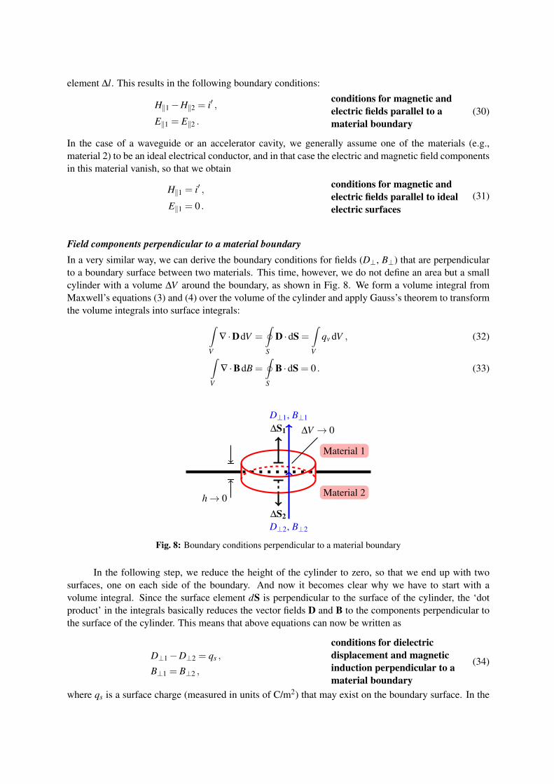
Field components perpendicular to a material boundaryIn a very similar way, we can derive the boundary conditions for fields (D⊥, B⊥) that are perpendicularto a boundary surface between two materials. This time, however, we do not define an area but a smallcylinder with a volume ∆V around the boundary, as shown in Fig. 8. We form a volume integral fromMaxwell’s equations (3) and (4) over the volume of the cylinder and apply Gauss’s theorem to transformthe volume integrals into surface integrals:∫
V
∇ ·DdV =∮S
D ·dS =∫V
qv dV , (32)
∫V
∇ ·BdB =∮S
B ·dS = 0 . (33)
∆S2
∆S1
D⊥1, B⊥1
D⊥2, B⊥2
h→ 0
∆V → 0
Material 1
Material 2
Fig. 8: Boundary conditions perpendicular to a material boundary
In the following step, we reduce the height of the cylinder to zero, so that we end up with twosurfaces, one on each side of the boundary. And now it becomes clear why we have to start with avolume integral. Since the surface element dS is perpendicular to the surface of the cylinder, the ‘dotproduct’ in the integrals basically reduces the vector fields D and B to the components perpendicular tothe surface of the cylinder. This means that above equations can now be written as
D⊥1−D⊥2 = qs ,
B⊥1 = B⊥2 ,
conditions for dielectricdisplacement and magneticinduction perpendicular to amaterial boundary
(34)
where qs is a surface charge (measured in units of C/m2) that may exist on the boundary surface. In the
case where material 2 is an ideal conductor, we obtain
D⊥1 = qs ,
B⊥1 = 0 .
conditions for dielectricdisplacement and magneticinduction perpendicular toideal electric surface
(35)
We note that when the fields are parallel to a boundary surface, the electric and magnetic fields areused in the boundary conditions, whereas when they are perpendicular to the boundary surface, we havea condition for the dielectric displacement and the magnetic induction. This means that, for instance, thetangential electric field E‖ may be smooth across a boundary but there will be a jump in the dielectricdisplacement D‖ if there are different relative dielectric constants εr in the two materials. Similarly,the component of the magnetic induction B⊥ perpendicular to a surface may be smooth, whereas themagnetic field H⊥ will jump if the two materials have different relative magnetic field constants µr.
2 Electromagnetic wavesIn this section, we shall derive the general form of the wave equation and then restrict ourselves tophenomena that are harmonic in time. Since RF systems mostly deal with sinusoidal waves, we shallbe able to explain and understand most of the relevant phenomena with this approach. This includes the‘skin effect’, the propagation of energy, RF losses, and acceleration via travelling waves.
2.1 The wave equationWe start with the simplification of looking only at homogeneous, isotropic media, meaning we assumethat the electromagnetic fields ‘see’ the same material constants (µ , ε , κ) in all directions. With thisassumption, Maxwell’s equations can be conveniently expressed in terms of only E and H:
∇×H = κE+ ε∂E∂ t
, (36)
∇×E =−µ∂H∂ t
, Maxwell’s equations (37)
∇ ·E =qv
ε, (38)
∇ ·H = 0 . (39)
The curl of Eq. (37) together with Eq. (36), and the curl of Eq. (36) together with Eqs. (37) and (38)result in the general wave equations for a homogeneous medium
∇2E−∇(∇ ·E) = µκ
ddt
E+µεd2
dt2 E ,
∇2H = µκ
ddt
H+µεd2
dt2 H .
wave equations in ahomogeneous medium (40)
In the case of waveguides and cavities, we can simplify these equations even further by considering onlythe fields inside the waveguide or cavity, which exist in a non-conducting medium (κ = 0) and a charge-free volume (∇ ·E = 0):
∇2E = µε
d2
dt2 E ,
∇2H = µε
d2
dt2 H .
wave equations in anon-conducting, charge-freehomogeneous medium
(41)
2.2 Complex notation for time-harmonic fieldsThe already compact wave equations in Eq. (41) can be simplified even further by taking into accountthe fact that in RF engineering one usually deals with time-harmonic signals, which are sometimesmodulated in phase or amplitude. We can therefore introduce the complex notation for electric andmagnetic fields. We start by assuming a time-harmonic electric field with amplitude E0 and phase ϕ ,
E(t) = E0 cos(ωt +ϕ) , (42)
which we can interpret as the real part of a complex expression,
E(t) = ℜ
E0eiϕeiωt= ℜE0 cos(ωt +ϕ)+ iE0 sin(ωt +ϕ) . (43)
In this form, we can easily separate the harmonic time dependence ωt from the phase information ϕ .The phase information can be merged into the amplitude by defining a ‘complex amplitude’ or ‘phasor’
E = E0eiϕ . (44)
We keep in mind that the real physical fields are obtained as the real part of the complex amplitude timeseiωt :
E0 cos(ωt +ϕ) = ℜ
Eeiωt . (45)
To simplify our writing, we skip the part with the harmonic time dependence and omit the tilde,which means that from now on all field quantities are written as complex amplitudes. In order to convinceyou that this really is a simplification, let us consider what happens to time derivatives when complexnotation is used:
ddt
Eeiωt = iωEeiωt . (46)
This means that all time derivatives in Maxwell’s equations and also in the wave equations cansimply be replaced by a multiplication by iω , and we are able to do this because the time dependence isalways harmonic. Only when we have to deal with transient events, such as the switching on of an RFamplifier or the sudden arrival of a beam in a cavity, do we have to go back the non-harmonic generalequations.
As our first application of the complex notation, we rewrite Maxwell’s equations as follows:
∇×H = iωεE , (47)
∇×E =−iωµH , Maxwell’s equations in (48)
∇ ·E =ρV
ε, complex notation (49)
∇ ·H = 0 , (50)
where the complex dielectric constant ε is defined as
ε = ε′− iε ′′ = ε
(1− i
κ
ωε
). complex dielectric constant (51)
We note that ε is complex only in a conducting medium. We can now proceed to write the general waveequations in complex form:
∇2E−∇(∇ ·E) =−k2E , general complex (52)
∇2H =−k2H . wave equations (53)

Here also, we note that the complex wavenumber k becomes real in the case of a non-conducting medium:
k2 = ω2µε = ω
2µε
(1− i
κ
ωε
). complex wavenumber (54)
Finally, we simplify the wave equations again for the case of a non-conducting, charge-free medium andobtain
∇2E =−k2E , complex wave equations in a non-
(55)
∇2H =−k2H , conducting, charge-free medium
(56)
with
k2 = ω2µε =
ω2
c2 . free-space wavenumber (57)
On the way, we have also introduced a simple definition for the speed of light, c = 1/√
µε , inEq. (57).
2.3 Plane wavesAs an introduction to the theory of electromagnetic waves, we look at a very simple case, that of so-calledplane waves. We assume again that we are in a homogeneous, isotropic, linear medium and that there areno charges or currents, which means that Eqs. (52) and (53) apply. Furthermore—for a plane wave—weassume that the field components depend only on one coordinate (e.g., z). The solution of the harmonicwave equations (52) and (53) can then be written as a superposition of two waves
Ex(z) =C1e−γz +C2e+γz ,
Hy(z) =1Z
(C1e−γz +C2e+γz) , (58)
one of which propagates in the positive and one in the negative z direction. The complex propagationconstant γ has a real component α , which describes the damping in a lossy material, and a complexcomponent iβ , which describes the propagation of the wave. The relation between the propagationconstant γ and the wavenumber k is
γ = α + iβ = ik = iω√
µε . propagation constant (59)
We already know that time-harmonic electric and magnetic fields are linked via Maxwell’s equa-tions, which means that their amplitudes have a certain fixed ratio to each other. This ratio has beenintroduced in Eq. (58) as the wave impedance Z, the ratio between the electric and magnetic field ampli-tudes
Z =Ey
Hz=
õ
ε, complex wave impedance (60)
which becomes real in the absence of lossy material. The wave impedance of free space is given by
Z0 =
õ0
ε0≈ 377Ω . free-space wave impedance (61)

2.4 Skin depthWhen electromagnetic waves encounter a conducting (lossy) material, we have to evaluate the bound-ary conditions (see Section 1.5), and we find that the wave amplitudes are attenuated suddenly by anattenuation constant α . In the RF case we can assume that
κ
ωε 1 , (62)
which means that the complex wavenumber (54) and, obviously, also the complex dielectric constant(51) are dominated by their imaginary parts, so that we can write
ε ≈−iε ′′ =−iκ
ωor k2 =−iωµκ , (63)
which is actually equivalent to neglecting the displacement current. Using Eq. (59), we can then writethe propagation constant as
γ = α + iβ = ik = iω
√−iµκ
ω= (1+ i)
√κµω
2, (64)
which defines the attenuation constant α . The ‘skin depth’ is then defined as the distance after which thewave amplitudes have been attenuated by a factor 1/e≈ 36.8%:
δs =1α
=
√2
ωµκ. skin depth (65)
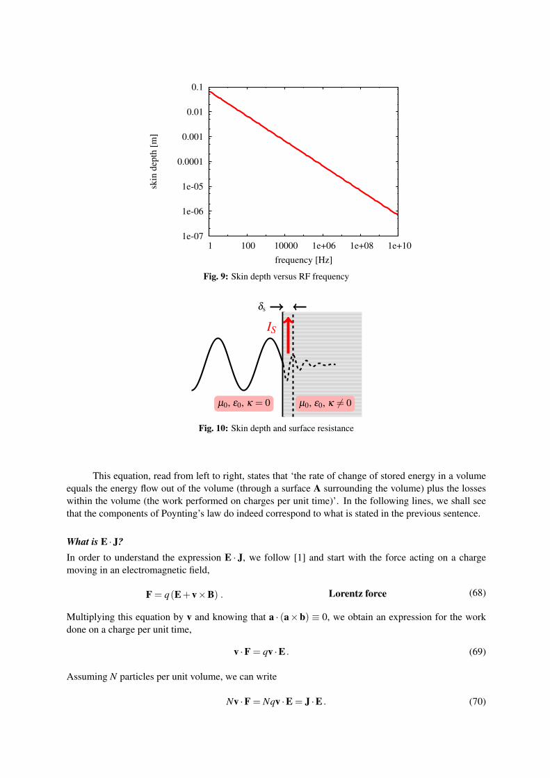
Knowing the value of the skin depth is crucial for the design of RF equipment. Let us assume thatwe want to build an accelerating cavity that resonates at 500 MHz. Since high-quality copper is quiteexpensive, we consider the possibility of constructing the cavity out of steel and then copper-plating theinterior in order to obtain a good quality factor and reduce the losses in the surface. From Eq. (65), wecalculate that the skin depth in copper is approximately 3 µm. Depending on how well the copper platingis done by the plating company, we can now define the thickness of the copper layer that is needed onthe inside of the cavity. Typically, around 10–20 times the skin depth is chosen as the plating thickness.Figure 9 shows the dependence of the skin depth on the RF frequency.
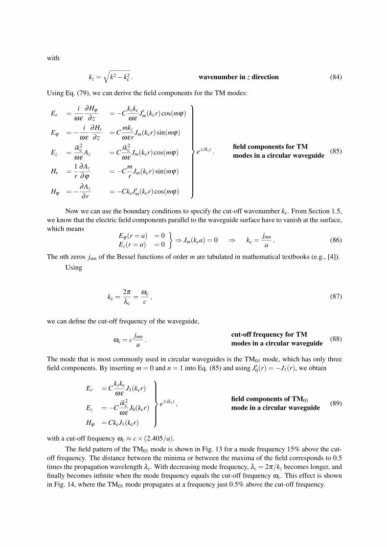
Furthermore, the skin depth allows us to calculate the losses in the surface easily. For a wavetravelling parallel to a conducting surface, one can define a surface resistance by assuming a constantcurrent density in a layer of the surface material equivalent to the skin depth, as shown in Fig. 10:
Rsurf =1
κδs[Ω] . surface resistance (66)
This value has to be multiplied by l/w to obtain the full RF resistance, where l is the length of theconducting wall and w is its width.
2.5 Energy and transport of energyWe start this section by presenting Poynting’s law, and then explain its components. Poynting’s law statesnothing more than the conservation of electromagnetic energy:
− ddt
∫V
wdV =∫A
S ·dA+∫V
E ·JdV . Poynting’s law (67)
1e-07
1e-06
1e-05
0.0001
0.001
0.01
0.1
1 100 10000 1e+06 1e+08 1e+10
skin
dep
th [
m]
frequency [Hz]
Fig. 9: Skin depth versus RF frequency
δs
IS
µ0, ε0, κ 6= 0µ0, ε0, κ = 0
Fig. 10: Skin depth and surface resistance
This equation, read from left to right, states that ‘the rate of change of stored energy in a volumeequals the energy flow out of the volume (through a surface A surrounding the volume) plus the losseswithin the volume (the work performed on charges per unit time)’. In the following lines, we shall seethat the components of Poynting’s law do indeed correspond to what is stated in the previous sentence.
What is E ·J?In order to understand the expression E · J, we follow [1] and start with the force acting on a chargemoving in an electromagnetic field,
F = q(E+v×B) . Lorentz force (68)
Multiplying this equation by v and knowing that a · (a×b) ≡ 0, we obtain an expression for the workdone on a charge per unit time,
v ·F = qv ·E . (69)
Assuming N particles per unit volume, we can write
Nv ·F = Nqv ·E = J ·E . (70)

Therefore the expression J ·E must be equal to the work done on charges per unit time and unit volume,or, in other words, the loss of electromagnetic energy per unit volume.
The Poynting vector S and the energy density w
These quantities can be understood by manipulating Maxwell’s equations (compare, e.g., [2]). We mul-tiply Eq. (1) by E:
E ·J = E · (∇×H)−E · ∂D∂ t
. (71)
Using Eq. (D.1), this can be rewritten as
E ·J = H · (∇×E)−∇ · (E×H)−E · ∂D∂ t
. (72)
Using the second of Maxwell’s equations (2) and assuming time-invariant µ and ε , we can write
E ·J =−∇ · (E×H)− ∂
∂ t
(12
E ·D+12
H ·B). (73)
Applying a volume integral together with Gauss’s theorem (16) and rearranging the elements ofthe equation, we end up with
− ∂
∂ t
∫V
(12
E ·D+12
H ·B)
dV
=∫
A(E×H) ·dA+
∫V
E ·JdV ,
Poynting’s law (74)
which can be compared directly with Eq. (67). On the left-hand side we have the definition of the energydensity,
w = wel +wmag =12
E ·D+12
B ·H ,electric and magnetic energydensity (75)
and from the right-hand side we obtain the definition of the energy flux density, or the Poynting vector S,
S = E×H . Poynting vector (76)
The Poynting vector gives us the direction in which an electromagnetic wave transports energy,and from the cross product we understand that this direction is always perpendicular to the electric andmagnetic field components. This is consistent with Section 2.3, where we found that the field components(Ex, Hy) of a plane wave (see Eq. (58)) are perpendicular to the direction of propagation (z).
In the above derivation, we have used Maxwell’s equations in their general form, meaning withtime derivatives. In the case of the complex notation, the definitions of the energy density and Poyntingvector have to be modified as follows (for a proof, see [2] or [3]):
w = wel +wmag =14
E ·D∗+ 14
B ·H∗ ,electric and magnetic energydensity in complex notation (77)
S =12(E×H∗) . complex Poynting vector (78)

3 Electromagnetic waves in waveguidesIn this section, we derive the field components of electromagnetic waves that propagate in waveguides.The same principle can then be used to calculate the standing-wave pattern in an accelerating cavity,which is nothing more than a superposition of two waves travelling in opposite directions.
3.1 Classification of modes in waveguides and cavitiesBefore we start to solve the wave equation, we need to introduce a classification of the field patterns thatcan be found in waveguides and cavities.
TMmnp modes, or Emnp modesThese modes have no magnetic field in the direction of propagation (z) and are therefore often calledtransverse magnetic, or TM, modes. On the other hand, they have an electric field component that isparallel to z, hence the equivalent name E modes.
The indices m, n, p indicate the number of zeros or variations in the three directions of a coordinatesystem. In the case of a waveguide, only the first two indices are used, whereas in the case of a cavity,owing to the standing-wave pattern along z, all three are needed for a complete description. In the caseof a circular waveguide or cavity, the indices indicate the following:
m, number of full-period variations of the field components in the azimuthal direction. For circularlysymmetric geometries, E, B ∝ cos(mϕ), sin(mϕ).
n, number of zeros (xmn) of the axial field component in the radial direction. For circularly symmetricgeometries, Ez, Bz ∝ Jm(xmnr/Rc).
p, number of half-period variations of the field components in the longitudinal direction, with E,B ∝ cos(pπz/l), sin(pπz/l).
The functions Jm introduced above are Bessel functions of the first kind and of mth order, and can befound in mathematical textbooks. The first three orders are shown in Fig. 11.
Fig. 11: Bessel functions of the first kind up to order 2

TEmnp modes, or Hmnp modesHere, there is no electric field in the direction of propagation z, hence the name transverse electric, orTE, modes. In analogy to the E modes, H modes have a magnetic field component parallel to z. Theindices have the same meaning as above.
TEM modesThis class of modes has neither an electric nor a magnetic field component in the direction of propagation.They can exist between two isolated conductors, for example in a coaxial line. The advantage of TEMmodes is that waves of any frequency can propagate, whereas TE and TM modes always have a cut-offfrequency, below which they are damped exponentially (more on this later). However, the disadvantageof coaxial lines is that the losses in the two conductors are generally higher than in rectangular or circularwaveguides.
3.2 Solution of the wave equation in a cylindrical waveguideInstead of trying to find solutions for all six vector components of the electric and magnetic fields, onecan simplify the problem by using a vector potential A (without any physical meaning) that has only onecomponent. One can then quickly derive all six field components from this vector potential.
It can be shown that only two types of modes can exist in waveguides: TM and TE modes, asintroduced above. For each mode type, we introduce a vector potential A as follows. Since H and E aredivergence-free, and since ∇ · (∇×a)≡ 0, we can write
HTM = ∇×ATM with ETM =− iωε
∇× (∇×ATM) , vector potential for TM waves (79)
ETE = ∇×ATE with HTE =i
ωµ∇× (∇×ATE) . vector potential for TE waves (80)
In both cases the vector potential obeys the wave equation
∇2A =−k2A with k2 = ω
2µε , (81)
which can then be solved for various coordinate systems and has only one vector component, in thedirection of propagation:
A = Azez . (82)
a
z
Fig. 12: Geometry of a circular waveguide
Circular waveguidesIn a circular waveguide, as shown in Fig. 12, the vector potentials for the TE and TM modes are identical:
ATM/TEz =CJm(kcr)cos(mϕ)e±ikzz , vector potential for circular waveguide (83)
with
kz =√
k2− k2c . wavenumber in z direction (84)
Using Eq. (79), we can derive the field components for the TM modes:
Er =i
ωε
∂Hϕ
∂ z=−C
kzkc
ωεJ′m(kcr)cos(mϕ)
Eϕ =− iωε
∂Hr
∂ z=C
mkz
ωεrJm(kcr)sin(mϕ)
Ez =ik2
c
ωεAz =C
ik2c
ωεJm(kcr)cos(mϕ)
Hr =1r
∂Az
∂ϕ=−C
mr
Jm(kcr)sin(mϕ)
Hϕ =−∂Az
∂ r=−CkcJ′m(kcr)cos(mϕ)
e±ikzz .field components for TMmodes in a circular waveguide (85)
Now we can use the boundary conditions to specify the cut-off wavenumber kc. From Section 1.5,we know that the electric field components parallel to the waveguide surface have to vanish at the surface,which means
Eϕ(r = a) = 0Ez(r = a) = 0
⇒ Jm(kca) = 0 ⇒ kc =
jmn
a. (86)
The nth zeros jmn of the Bessel functions of order m are tabulated in mathematical textbooks (e.g., [4]).
Using
kc =2π
λc=
ωc
c, (87)
we can define the cut-off frequency of the waveguide,
ωc = cjmn
a.
cut-off frequency for TMmodes in a circular waveguide (88)
The mode that is most commonly used in circular waveguides is the TM01 mode, which has only threefield components. By inserting m = 0 and n = 1 into Eq. (85) and using J′0(r) =−J1(r), we obtain
Er =Ckzkc
ωεJ1(kcr)
Ez =−Cik2
c
ωεJ0(kcr)
Hϕ =CkcJ1(kcr)
e±ikzz ,
field components of TM01mode in a circular waveguide (89)
with a cut-off frequency ωc ≈ c× (2.405/a).
The field pattern of the TM01 mode is shown in Fig. 13 for a mode frequency 15% above the cut-off frequency. The distance between the minima or between the maxima of the field corresponds to 0.5times the propagation wavelength λz. With decreasing mode frequency, λz = 2π/kz becomes longer, andfinally becomes infinite when the mode frequency equals the cut-off frequency ωc. This effect is shownin Fig. 14, where the TM01 mode propagates at a frequency just 0.5% above the cut-off frequency.

λz/2TM01
Fig. 13: Field lines of a TM01 mode in a circular waveguide with ω = 1.15ωc. Solid lines, electricfield lines; dashed lines, magnetic field lines. The brightness of the background is proportional tothe norm of the field vector: light areas indicate high-field regions of the magnetic field in the leftplot and of the electric field in the right plot.
TM01Fig. 14: Field lines of a TM01 mode in a circular waveguide with ω = 1.005ωc. Solid lines, electricfield lines; dashed lines, magnetic field lines. The brightness of the background is proportional tothe norm of the field vector: light areas indicate high-field regions of the magnetic field in the leftplot and of the electric field in the right plot.
Rectangular waveguidesThe derivation of the fields in a rectangular waveguide follows the same principle as that used in theprevious section for circular waveguides. In a rectangular waveguide, as shown in Fig. 15, two differentvector potentials are needed to describe the TE and TM modes:
a
b z
x
y
Fig. 15: Geometry of a rectangular waveguide with transverse dimensions a and b
ATMz =C sin(kxx)sin(kyy)e±ikzz ,
vector potential for TM wavesin a rectangular waveguide (90)

ATEz =C cos(kxx)cos(kyy)e±ikzz ,
vector potential for TE wavesin a rectangular waveguide (91)
where
kz =√
k2− k2c , with k2
c = k2x + k2
y . wavenumber in z direction (92)
We note that the position of the origin of the coordinate system is linked to the sine and cosine terms inEqs. (90) and (91). The fields derived from the vector potentials have to fulfil the boundary conditionson the waveguide walls. So if, for instance, we were to choose the origin in the centre of the waveguide,then the sine and cosine expressions would have to be exchanged to account for the changed symmetrieswith respect to the coordinate axes. Using Eq. (79) again, we derive the field components for the TMmodes:
Ex =i
ωε
∂Hy
∂ z=±C
kz
ωεcos(kxx)sin(kyy)
Ey =− iωε
∂Hx
∂ z=±C
kz
ωεsin(kxx)cos(kyy)
Ez =i(k2
z − k2)
ωεATM
z =Ci(k2
z − k2)
ωεsin(kxx)sin(kyy)
Hx =∂ATM
z
∂y=Cky sin(kxx)cos(kyy)
Hy =−∂ATM
z
∂x=−Ckx cos(kxx)sin(kyy)
e±ikzz .
field components forTM modes in arectangular waveguide
(93)
Using the boundary conditions, we can specify the wavenumbers kx and ky:
Ey(x = a) = 0Ez(x = a) = 0
⇒ kx =
mπ
aand m = 0,1,2, . . . , (94)
Ex(y = b) = 0Ez(y = b) = 0
⇒ ky =
nπ
band n = 0,1,2, . . . , (95)
and the cut-off frequency for a rectangular waveguide is
ωc = ckc = c√
k2x + k2
y = cπ
√(ma
)2+(n
b
)2.
cut-off frequency for TMmodes in a rectangularwaveguide
(96)
The usual convention is to have a > b, and in this case the TE10 mode is the mode with the lowestcut-off frequency. It is also the only mode that propagates in a relatively large frequency band, fromf TE,10c to 2 f TE,10
c , which is why it is the mode most commonly used in rectangular waveguides. Thefields of the TE modes can be derived from the TE vector potential using the same procedure.
3.3 Wave propagation and dispersion relationIn Figs. 13 and 14, we have seen that the propagation wavelength λz of a waveguide mode is determinedby its frequency and by how far the mode frequency is above the cut-off frequency of the waveguide. Ifthe propagation wavelength depends on the mode frequency, we can assume that the phase velocity of aparticular mode also depends on the mode frequency. This relationship is called the dispersion relationand, using the definition of the wavenumber in Eq. (84), we can write

k2z = k2− k2
c =ω2−ω2
c
c2 =ω2
v2ph, dispersion relation (97)
from which we can immediately see that:
– kz can be real only if the mode frequency ω is above the cut-off frequency ωc;– for ω < ωc, the mode cannot propagate and the fields are exponentially damped.
We also have a definition of the phase velocity, which is the speed at which the maxima and minima ofthe field patterns move along the waveguide:
vph =ω
kz= c2 ω2
ω2−ω2c. phase velocity (98)
This is not to be confused with the speed with which the wave actually propagates in the waveguide. Thedispersion relation is usually plotted in the form of a ‘Brillouin diagram’, as shown in Fig. 16.
kz0
ω
vph > c
ωc
vph = c
vph =ω
kz
Fig. 16: Dispersion relation in a waveguide. The dotted line shows the case vph = c.
The slope of the dispersion relation is the group velocity
vgr =dω
dkz, group velocity (99)
which gives the velocity with which a signal or energy is transported along the waveguide. From Fig. 16,we can conclude that:
– Each frequency has a certain phase velocity and group velocity, which means that signals with afrequency bandwidth will become deformed while travelling along a waveguide. With the help ofthe dispersion relation, we can easily quantify how much deformation will occur.
– The phase velocity vph is always larger than the velocity of light c, and at cut-off (ω = ωc) it evenbecomes infinite (kz = 0 and vph→ ∞).
– For acceleration, one needs synchronism between the phase velocity (the speed of the field pattern)and the velocity of the particles, which implies that acceleration in waveguides is impossible.
– Information and therefore energy travel at the group velocity, which is always slower than thespeed of light.
3.4 Attenuation of waves (power loss method)Up to this point, we have assumed perfect electrical conductors as the boundaries of our waveguides. Realwaveguides and cavities have a certain resistance, and the fields therefore penetrate into the conductors,which significantly complicates the solution of the wave equation. However, we have seen in Section2.4 that the skin depth in metals is very much smaller than the RF wavelength. This means that wecan reasonably assume that the field patterns in a waveguide with ideal boundaries and in a waveguidewith resistive metal boundaries will be practically identical (of course, only for good conductors such ascopper or aluminium). In order to calculate the attenuation of waves, we can therefore use the fields ofa waveguide with ideal electrical boundaries. From the magnetic field, we calculate the induced currentin the waveguide walls, and then apply the resistance of the real material to calculate the losses and thenthe damping of the wave. This principle is called the power loss method and is a simplified method forcalculating RF losses on the surfaces of good conductors.
We start by defining the power that is lost per unit length along the longitudinal axis of the wave-guide,
P′ =−dPdz
. (100)
From
E,H ∝ e−αz ⇒ P ∝ e−2αz , (101)
we immediately obtain
P′ =−dPdz
= 2αP (102)
and thus the definition of the attenuation constant
α =P′
2P. attenuation constant (103)
In the next steps, we need to derive expressions for the power P transported through the waveguide,and the power loss per unit length P′. Using the field components of the TM01 mode given in Eq. (89)and the definition of the complex Poynting vector in Eq. (78), we obtain
P =12
∫A
(E×H∗) ·dA =12
a∫0
2π∫0
ErH∗ϕr dr dϕ =C2kzk2
cπa2J21 (kca)
ωε, (104)
where we have used
a∫0
J21 (kcr)r dr =
a2
2J2
1 (kca) . (105)
In order to calculate the losses on the waveguide surface, we first need to know the surface currentsthat flow within the skin depth. For this purpose, we make use of Ampère’s law, as shown in Fig. 17:
∮c
H ·dl = I =∮c
J · (δs dl) . Ampère’s law (106)

Hϕ = 0 a∆ϕHϕ
δs
κ = κAl
κ = 0
Fig. 17: Ampère’s law applied to calculate the surface currents in a circular waveguide
Since the magnetic field has only an azimuthal component, we obtain
Hϕ(r = a,z) =CkcJ1(kca)e−ikzz = Jz(z)δs . (107)
The power density (in W/m3) in the waveguide wall is given by
pv =12
E ·J∗ = 12κ
JzJ∗z =∂ 3P
(∂ r)(r ∂ϕ)(∂ z), power density (108)
from which we can write an expression for the power loss per unit length. Together with Eq. (107), weobtain
P′ =∂P∂ z
=
a+δs∫a
2π∫0
pvr dr dϕ =πaC2k2
cJ21 (kca)
κδs, power loss per unit length (109)
where we have used the fact that δs a to simplify the evaluation of the integral. Now we insertEqs. (104) and (109) into Eq. (103) and obtain an expression for the attenuation of a TM01 mode in acircular waveguide,
α =P′
2P=
Rsurf
Z0a√
1− ( fc/ f )2.
attenuation of TM01 mode incircular waveguide (110)
In the expression above, we have used the definition of the surface resistance given in Eq. (66) and thedefinition of the free-space wave impedance Z0 given in Eq. (61).
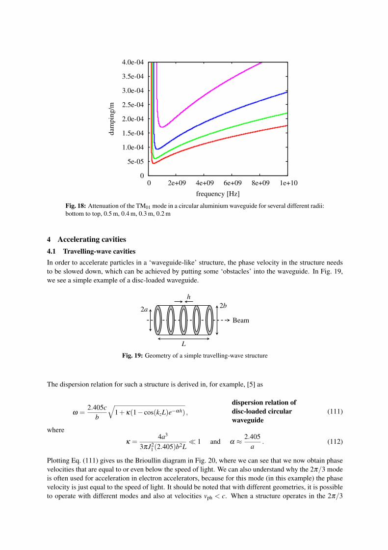
As an example, we have plotted the attenuation constant for an aluminium waveguide in Fig. 18,where we can see that for this type of waveguide:
– Large-diameter waveguides result in smaller losses, which means that a cost optimum has to befound between the cost of the waveguide, its space requirements, and the losses.
– The minimum losses occur when the operating frequency of the TM01 mode is a factor of√
3above the cut-off frequency (try to prove this!).
0
5e-05
1.0e-04
1.5e-04
2.0e-04
2.5e-04
3.0e-04
3.5e-04
4.0e-04
0 2e+09 4e+09 6e+09 8e+09 1e+10
dam
pin
g/m
frequency [Hz]
Fig. 18: Attenuation of the TM01 mode in a circular aluminium waveguide for several different radii:bottom to top, 0.5 m, 0.4 m, 0.3 m, 0.2 m
4 Accelerating cavities4.1 Travelling-wave cavitiesIn order to accelerate particles in a ‘waveguide-like’ structure, the phase velocity in the structure needsto be slowed down, which can be achieved by putting some ‘obstacles’ into the waveguide. In Fig. 19,we see a simple example of a disc-loaded waveguide.
Beam
L
2a 2bh
Fig. 19: Geometry of a simple travelling-wave structure
The dispersion relation for such a structure is derived in, for example, [5] as
ω =2.405c
b
√1+κ(1− cos(kzL)e−αh) ,
dispersion relation ofdisc-loaded circularwaveguide
(111)
where
κ =4a3
3πJ21 (2.405)b2L
1 and α ≈ 2.405a
. (112)
Plotting Eq. (111) gives us the Brioullin diagram in Fig. 20, where we can see that we now obtain phasevelocities that are equal to or even below the speed of light. We can also understand why the 2π/3 modeis often used for acceleration in electron accelerators, because for this mode (in this example) the phasevelocity is just equal to the speed of light. It should be noted that with different geometries, it is possibleto operate with different modes and also at velocities vph < c. When a structure operates in the 2π/3

mode, this means that the RF phase shifts by 2π/3 per cell, or, in other words, one RF period extendsover three cells.
kz0
ω
2π
3L
Reflected wave
vph = c
−2π
L2π
L−π
Lπ
L
ωc
ωπ
Fig. 20: Dispersion diagram for a disc-loaded travelling-wave structure. Here, the chosen operatingpoint is vph = c and kz = 2π/3L.
By attaching an input and an output coupler to the outermost cells of the structure, we obtain ausable accelerating structure. Since the particles gain energy in every cell, the electromagnetic wavebecomes increasingly damped along the structure. It is then extracted via the output coupler and dumpedin an RF load. If one is interested in obtaining the maximum possible accelerating gradient in each cell,then one can counteract the decreasing fields by changing the bore radius from cell to cell. The idea isto slow down the group velocity from cell to cell and obtain a ‘constant-gradient’ structure, rather than a‘constant-impedance’ structure where the bore radius is kept constant. Other optimizations, for examplefor maximum efficiency, are also possible.
4.2 Standing-wave cavitiesOne obtains a cylindrical standing-wave structure by simply closing both ends of a circular waveguidewith electric walls. This yields multiple reflections on the end walls until a standing-wave pattern is es-tablished. Owing to the additional boundary conditions in the longitudinal direction, we obtain another‘restriction’ on the existence of electromagnetic modes in the structure. Whereas a longitudinally opentravelling-wave structure allows all frequencies and all cell-to-cell phase variations on the dispersioncurve, now only certain ‘loss-free’ modes (still assuming perfectly conducting walls) with discrete fre-quencies and discrete phase changes can exist in a cavity. If RF power is fed in at a different frequency,then the fields excited are damped exponentially, similarly to the modes below the cut-off frequency of awaveguide.
The corresponding dispersion relation for a standing-wave cavity can again be found in textbooks(see [5] and also [6]). However, it is necessary to pay attention to whether the structure under consider-ation has magnetic or electric cell-to-cell coupling and what kind of end cell is assumed in the analysis.The most common form of the dispersion relation is derived from a coupled-circuit model with N + 1cells. Usually the model has half-cell terminations on both ends of the chain, representing the behaviourof an infinite chain of electrically coupled resonators (compare the original paper by Nagle et al. [7]):
ωn =ω0√
1+ k cos(nπ/N), n = 0,1, . . . ,N.
dispersion relation forhalf-cell-terminatedstanding-wave structure
(113)
Assuming an odd number of cells, ω0 is the frequency of the π/2 mode and of an uncoupled single cell;k is the cell-to-cell coupling constant, and nπ/N is the phase shift from cell to cell. For k 1, which isusually fulfilled, the coupling constant is given by

k =ωπ mode−ω0 mode
ω0. coupling constant (114)
Two characteristics of the dispersion curve are worth noting:
– The total width of the frequency band of the mode, ωπ mode−ω0 mode, is independent of the numberof cells, which means that we can determine the cell-to-cell coupling constant by measuring thecomplete structure (but this is only true if all coupling constants are equal).
– For electric coupling, the 0 mode has the lowest frequency and the π mode has the highest. Inthe case of magnetic coupling, this behaviour is reversed, and one can find the correspondingdispersion curve by changing the sign before the coupling constant in Eq. (113).
In Fig. 21, we plot the dispersion curve for a seven-cell (half-cell-terminated) magnetically coupledstructure according to Eq. (113).
0 ππ/2
ω0√1− k
ω0√1+ k
Fig. 21: Dispersion diagram for a standing-wave structure with seven magnetically coupled cells
In practice, one usually has cavities with full-cell termination, and in this case one has to detunethe frequences of the end cells to obtain a flat field distribution in the cavity [8]. In this case it is possibleto have a flat field distribution for either the 0 mode or the π mode but not for both at the same time,because the end cells have to be detuned by different amounts in the two cases [9].
4.3 Standing wave versus travelling waveThe principal difference between the two types of cavity is in how and how fast the cavities are filled withRF power. Travelling-wave structures are filled ‘in space’, which means that, basically, cell after cell isfilled with power. For the following estimations, we assume a frequency in the range of hundreds ofmegahertz. The filling of a travelling-wave structure typically takes place with a speed of approximately1–3% of the speed of light and results in total filling times in the submicrosecond range. Standing-wavestructures, on the other hand, are filled ‘in time’: the electromagnetic waves are reflected at the endwalls of the cavity and slowly build up a standing-wave pattern of the desired amplitude. For normal-conducting cavities, the time required for this process is typically in the range of tens of microseconds.For superconducting cavities, the filling time can easily go into the millisecond range (depending on therequired field level, the accelerated current, and the cavity parameters). This means that for applicationsthat require very short beam pulses (< 1 µs), travelling-wave structures are much more power-efficient.For longer pulses (> n×10 µs), both types of structures can be optimized to achieve similar efficienciesand costs.
Since one can have extremely short RF pulses in a travelling-wave structure, one can obtain muchhigher peak fields than in a standing-wave structure. This is demonstrated by the accelerating structuresfor CLIC [10], which have reached values of approximately 100 MV/m (limited by electrical break-down), whereas the design gradient for the superconducting (standing-wave) cavities for the ILC [11] isjust slightly above 30 MV/m (this value is generally limited by field emission and by quenches causedby the peak magnetic field).
Travelling-wave structures can, theoretically, be designed for non-relativistic particles. In existingaccelerators, however, they are mostly used for relativistic particles. Low-beta acceleration is typicallyperformed with standing-wave cavities.
Because of the lack of an obvious criterion (other than the pulse length or the particle velocity),an optimization and costing exercise has to be performed for each specific application in order to decidewhich structure is more efficient. Two excellent papers [12, 13] in which this exercise is performed canbe used as references.
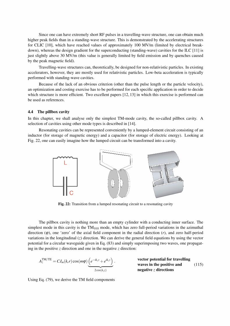
4.4 The pillbox cavityIn this chapter, we shall analyse only the simplest TM-mode cavity, the so-called pillbox cavity. Aselection of cavities using other mode types is described in [14].
Resonating cavities can be represented conveniently by a lumped-element circuit consisting of aninductor (for storage of magnetic energy) and a capacitor (for storage of electric energy). Looking atFig. 22, one can easily imagine how the lumped circuit can be transformed into a cavity.
Fig. 22: Transition from a lumped resonating circuit to a resonating cavity
The pillbox cavity is nothing more than an empty cylinder with a conducting inner surface. Thesimplest mode in this cavity is the TM010 mode, which has zero full-period variations in the azimuthaldirection (ϕ), one ‘zero’ of the axial field component in the radial direction (r), and zero half-periodvariations in the longitudinal (z) direction. We can derive the general field equations by using the vectorpotential for a circular waveguide given in Eq. (83) and simply superimposing two waves, one propagat-ing in the positive z direction and one in the negative z direction:
ATM/TEz =CJm(krr)cos(mϕ)
(e−ikzz + eikzz
)︸ ︷︷ ︸
2cos(kzz)
. vector potential for travellingwaves in the positive andnegative z directions
(115)
Using Eq. (79), we derive the TM field components
Er =i
ωε
∂Hϕ
∂ z= i2C
kzkr
ωεJ′m(krr)cos(mϕ)sin(kzz) ,
Eϕ =− iωε
∂Hr
∂ z=−i2C
mkz
ωεrJm(krr)sin(mϕ)sin(kzz) ,
Ez =ik2
r
ωεAz = i2C
k2r
ωεJm(krr)cos(mϕ)cos(kzz) ,
Hr =1r
∂Az
∂ϕ=−2C
mr
Jm(krr)sin(mϕ)cos(kzz) ,
Hϕ =−∂Az
∂ r=−2CkrJ′m(krr)cos(mϕ)cos(kzz) .
TM modes in a pillbox cavity (116)
In the case of standing-wave cavities, the term ‘cut-off’ frequency does not really make sense,so we have replaced the symbol kc by kr, indicating that we have a radial dependence of the axial fieldcomponent, which can also be interpreted as a radial wavenumber.
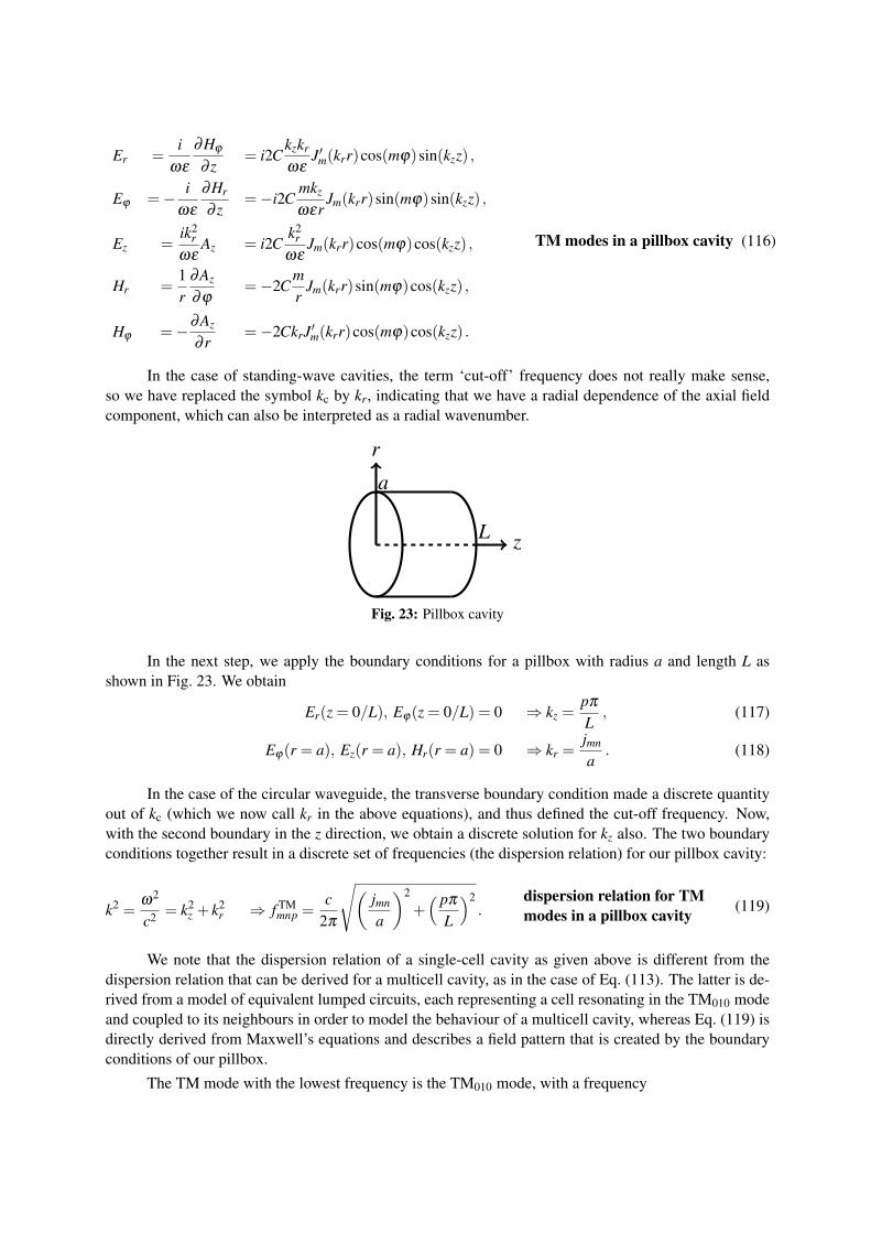
r
a
L z
Fig. 23: Pillbox cavity
In the next step, we apply the boundary conditions for a pillbox with radius a and length L asshown in Fig. 23. We obtain
Er(z = 0/L), Eϕ(z = 0/L) = 0 ⇒ kz =pπ
L, (117)
Eϕ(r = a), Ez(r = a), Hr(r = a) = 0 ⇒ kr =jmn
a. (118)
In the case of the circular waveguide, the transverse boundary condition made a discrete quantityout of kc (which we now call kr in the above equations), and thus defined the cut-off frequency. Now,with the second boundary in the z direction, we obtain a discrete solution for kz also. The two boundaryconditions together result in a discrete set of frequencies (the dispersion relation) for our pillbox cavity:
k2 =ω2
c2 = k2z + k2
r ⇒ f TMmnp =
c2π
√(jmn
a
)2
+( pπ
L
)2.
dispersion relation for TMmodes in a pillbox cavity (119)
We note that the dispersion relation of a single-cell cavity as given above is different from thedispersion relation that can be derived for a multicell cavity, as in the case of Eq. (113). The latter is de-rived from a model of equivalent lumped circuits, each representing a cell resonating in the TM010 modeand coupled to its neighbours in order to model the behaviour of a multicell cavity, whereas Eq. (119) isdirectly derived from Maxwell’s equations and describes a field pattern that is created by the boundaryconditions of our pillbox.
The TM mode with the lowest frequency is the TM010 mode, with a frequency

f TM010 =
2.405c2πa
,frequency of the TM010pillbox mode (120)
and its field components are
Ez =−i2Cj201
a2ωεJ0
(j01
ar)
= E0J0
(j01
ar),
Hϕ = 2Cj01
aJ1
(j01
ar)
=E0
Z0J1
(j01
ar).
field components of the TM010pillbox mode (121)
Figure 24 shows the field pattern of the TM010 mode, simulated by Superfish©.
Fig. 24: Field pattern of the TM010 mode in a pillbox cavity
4.5 Basic cavity parametersIn order to characterize and optimize cavities, we need some commonly used figures of merit, whichwe shall define here in general terms and then apply to our simple pillbox cavity. In the following, weassume that we are dealing with an axially symmetric cavity resonating in the TM010 mode.
4.5.1 Energy gain in a cavityFor particles traversing a cavity on axis, the electric field generally has the following form:
Ez(r = 0,z, t) = E(0,z)cos(ωt +ϕ) , (122)
which we can use to calculate the energy gain of a particle when it traverses the cavity,
∆W = q
L/2∫−L/2
E(0,z)cos(ωt +ϕ)
= qV0T cosϕ = qE0T Lcosϕ ,
energy gain in a cavity(Panofsky equation) (123)
where the cavity voltage is given by
V0 =
L/2∫−L/2
E(0,z)dz = E0 , cavity voltage (124)
and the ‘difficult mathematics’ has been lumped into the so-called transit time factor
T =
L/2∫−L/2
E(0,z)cos(ωt(z))dz
L/2∫−L/2
E(0,z)dz
− tanφ
L/2∫−L/2
E(0,z)sin(ωt(z))dz
L/2∫−L/2
E(0,z)dz︸ ︷︷ ︸=0 if E(0,z) is symmetric about z=0
.transit time factor (125)
This takes into account the fact that the RF electric field changes during the passage of the particles. Itgives the ratio between the energy gained in an RF field and in a DC field and is therefore always lessthan 1. We note that the Panofsky equation takes account of the changing velocity of the particles whenthey cross the accelerating gap. This makes the integrals in the above equations difficult to evaluate.Assuming that the velocity change of the beam particles during their passage is small, however, one cansay that
ωt ≈ ωzv=
2πzβλ
, (126)
which changes the expression for the transit time factor to (assuming that E(0,z) is symmetric aboutz = 0)
T =
L/2∫−L/2
E(0,z)cos(2πz/βλ )dz
L/2∫−L/2
E(0,z)dz
.transit time factor for smallvelocity changes (127)
The accelerating voltage Vacc is the voltage that the particle ‘sees’ when crossing the cavity andshould not be confused with the cavity voltage V0. We thus define
Vacc =V0T = E0LT . accelerating voltage (128)
4.5.2 Shunt impedanceThe shunt impedance tells us how much voltage a cavity will provide when a certain amount of poweris dissipated in the cavity walls. This is one of the parameters to be maximized in cavity design, since alarge shunt impedance reduces the power consumption of an RF cavity. The general definition is
Rs =V 2
0Pd
.shunt impedance (linacdefinition) (129)
The benefit of a high shunt impedance can easily be diminished by having a small transit time factor, be-cause in this case the cavity voltage cannot be used efficiently to transfer energy to the beam. Thereforeone usually tries to optimize both the shunt impedance and the transit time factor, which explains the
definition of the effective shunt impedance
R =(V0T )2
Pd. effective shunt impedance (130)
When comparing multicell structures operating at different frequencies, one is interested less inthe efficiency per cell (because the cell size depends on, for instance, the frequency chosen) than in theefficiency per unit length of the accelerating structure. For this reason, we define
Z =Rs
L=
E20
Pd/Lshunt impedance per unitlength (131)
and
ZT 2 =RL=
(E0T )2
Pd/L.
effective shunt impedance perunit length (132)
4.5.3 ‘Linac’ and ‘circuit’ definitions of shunt impedanceIt turns out that different communities of accelerator experts use different definitions of the shunt impedan-ce. Linac experts usually use the definitions presented above, whereas the people who deal with circularmachines generally use a definition that is derived from the lumped-circuit definition of a resonator (seeSection 4.7). In that definition, all shunt impedances are exactly half as large, following
Rcs =
V 20
2Pd.
shunt impedance (circuitdefinition) (133)
So, before you discuss shunt impedances with anyone, make sure that you are using the same definition.In order to mark the difference clearly, we use Rc
s in this text to identify when the circuit definition isbeing used.
4.5.4 3 dB bandwidth and quality factorThe quality factor Q describes the bandwidth of a resonator and is defined as the ratio of the reactivepower (stored energy) to the real power that is lost in the cavity walls:
Q =ω
∆ω=
ωWPd
. quality factor (134)
If a resonator were built with ideal electrical walls (zero electrical resistance), the resonance curvewould be a delta function at the resonance frequency. So, the bandwidth ∆ω would be zero and the qualityfactor would be infinite. In reality, even superconducting cavities have a certain surface resistance,which is why all our cavities have a certain bandwidth and a finite quality factor. Figure 25 shows atypical resonance curve measured with a network analyser. In a measurement of this kind, two antennaspenetrate the cavity. The first antenna sends an RF signal with a frequency sweep, and the second picksup the field level in the cavity. As a result, we obtain a plot of the field level versus frequency. Thebandwidth is defined as the frequency width of the resonance curve, measured as the distance betweenthe points where the field level has dropped by 50% (or −3 dB), as shown in Fig. 25.
Together with the shunt impedance, one can define another figure of merit, (R/Q), which is usedto maximize the energy gain in a cavity for a given stored energy:
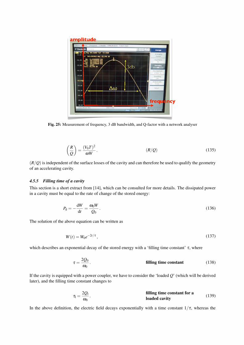
Fig. 25: Measurement of frequency, 3 dB bandwidth, and Q-factor with a network analyser
(RQ
)=
(V0T )2
ωW. (R/Q) (135)
(R/Q) is independent of the surface losses of the cavity and can therefore be used to qualify the geometryof an accelerating cavity.
4.5.5 Filling time of a cavityThis section is a short extract from [14], which can be consulted for more details. The dissipated powerin a cavity must be equal to the rate of change of the stored energy:
Pd =−dWdt
=ω0WQ0
. (136)
The solution of the above equation can be written as
W (t) =W0e−2t/τ , (137)
which describes an exponential decay of the stored energy with a ‘filling time constant’ τ , where
τ =2Q0
ω0. filling time constant (138)
If the cavity is equipped with a power coupler, we have to consider the ‘loaded Q’ (which will be derivedlater), and the filling time constant changes to
τl =2Ql
ω0.
filling time constant for aloaded cavity (139)
In the above definition, the electric field decays exponentially with a time constant 1/τ , whereas the
stored energy decays with a time constant 2/τ . Be aware that you can often find textbook definitions ofthe filling time constant where the stored energy decays with a time constant 1/τ .
4.6 Basic cavity parameters for a pillbox cavityAs a small exercise, in this section we calculate the cavity parameters that were defined in the previoussection for a pillbox cavity of length L and radius a. Since the TM010 mode has no z dependence, we cansimplify the expression for the transit time factor (127) to
T =
L/2∫−L/2
E(0,z)cos(2πz/βλ )dz
L/2∫−L/2
E(0,z)dz
=sin(πL/βλ )
πL/βλ.
transit time factor of a pillboxfor small velocity changes (140)
In the case of relativistic particles (β ≈ 1) and a cavity length L = λ/2, which is often chosen becausethe cavity can then be cascaded into a multicell structure, we obtain
T =2π= 0.64 .
transit time factor of a pillboxfor relativistic particles (141)
With real cavities, one usually tries to increase the transit time factor by shortening the accelerating gap.This can be done by introducing nose cones on the cavity walls, as shown in Fig. 22.
We use the power loss method again to calculate the quality factor of our pillbox cavity. To evaluateEq. (134), we need the stored energy and the power lost in the cavity walls. For the stored energy, weobtain
W =Wel +Wmag = 2Wel = 2∫V
14
E ·D∗ dV . (142)
With
Ez = E0J0
(j01ra
), (143)
we obtain
W =ε0
2
a∫0
2π∫0
L/2∫−L/2
E20 J2
0
(j01ra
)r dr dϕ dz =
12
E20 ε0πLa2J2
1 ( j01) . (144)
To calculate the dissipated power, we integrate Eq. (108) over a volume that consists of the inner surfaceof the pillbox times the skin depth:
Pd =δs
2κ
L/2∫−L/2
JzJ∗z︸︷︷︸(1/δs)2H2
ϕ (r=a,z)
2πadz+δs
κ
a∫0
JrJ∗r︸︷︷︸(1/δs)2
H2ϕ(r,z = 0)2πr dr (145)
=E2
0 πRsurfaZ2
0J2
1 ( j01)(a+L) , (146)
where we have made use of
Hϕ =E0
Z0J1
(j01ra
). (147)
Putting everything together, we obtain
Q0 =ωWPd
=Z2
0ω
2Rsurf
LaL+a
=1δs
LaL+a
∝√
ω . (148)

As we can see, the quality factor is a function of the material constants κ and µ (which are containedin ρs), the frequency, and the geometry of the cavity. We also note that for the same cavity shape, thequality factor increases with the frequency in proportion to
√ω .
The accelerating voltage in a pillbox cavity is given by
Vacc =V0T = E0LT = E0Lsin(πL/βλ )
πL/βλ, accelerating voltage in pillbox (149)
and is obviously a strong function of the transit time factor. It therefore depends on the gap length L andthe speed of the particles β . Owing to their high development costs, superconducting cavities are oftenused over large velocity ranges without changing their cell length, and this results in a velocity-dependentacceleration efficiency. Figure 26 shows (R/Q) ∝ (V0T )2 as a function of particle velocity for a five-cellsuperconducting cavity whose geometric cell length corresponds to a particle speed of β = 0.65.
Fig. 26: Dependence of (R/Q) on particle velocity for a five-cell superconducting cavity with ageometric β of 0.65 and a frequency of 704.4 MHz. Upper curve, π mode (see also [15]).
If the cavity is used over too large a velocity range, one may find areas where the passband modethat is closest to the π mode (here, the 4/5π mode) has a higher acceleration efficiency than the acceler-ating mode. These areas are highlighted in Fig. 26, and should be avoided when one is designing a linac.One should also be aware that the (R/Q) of the HOMs is highly dependent on the particle velocity.
Using the expressions for the accelerating voltage V0T (Eq. (149)) and the dissipated power Pd(Eq. (146)), we also obtain an analytical expression for the effective shunt impedance,
R =(V0T )2
Pd=
Z0
πRsurfJ21 ( j01)
sin(πL/βλ )
πL/βλ
L2
a(a+L).
effective shunt impedance of apillbox (150)
Finally, we calculate the frequency and (R/Q) using Eqs. (120), (150), and (148):
f TM010 =
2.405c2πa
, pillbox frequency (151)
(RQ
)=
2cωπJ2
1 ( j01)
sin(πL/βλ )
πL/βλ
La2 . pillbox (R/Q) (152)
As stated before, (R/Q) is indeed independent of any material parameters. However, it does depend onthe geometry of the cavity and the transit time factor.
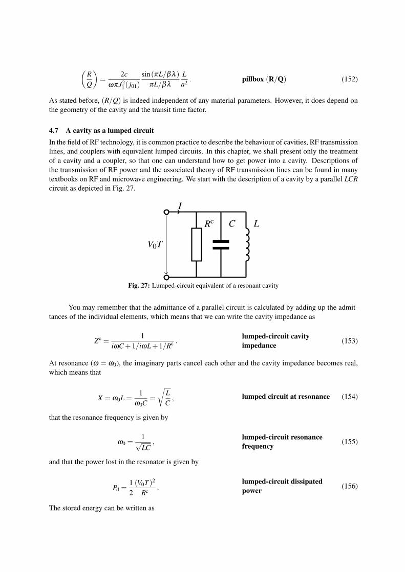
4.7 A cavity as a lumped circuitIn the field of RF technology, it is common practice to describe the behaviour of cavities, RF transmissionlines, and couplers with equivalent lumped circuits. In this chapter, we shall present only the treatmentof a cavity and a coupler, so that one can understand how to get power into a cavity. Descriptions ofthe transmission of RF power and the associated theory of RF transmission lines can be found in manytextbooks on RF and microwave engineering. We start with the description of a cavity by a parallel LCRcircuit as depicted in Fig. 27.
I
V0T
Rc C L
Fig. 27: Lumped-circuit equivalent of a resonant cavity
You may remember that the admittance of a parallel circuit is calculated by adding up the admit-tances of the individual elements, which means that we can write the cavity impedance as
Zc =1
iωC+1/iωL+1/Rc .lumped-circuit cavityimpedance (153)
At resonance (ω = ω0), the imaginary parts cancel each other and the cavity impedance becomes real,which means that
X = ω0L =1
ω0C=
√LC, lumped circuit at resonance (154)
that the resonance frequency is given by
ω0 =1√LC
,lumped-circuit resonancefrequency (155)
and that the power lost in the resonator is given by
Pd =12(V0T )2
Rc .lumped-circuit dissipatedpower (156)
The stored energy can be written as

W =12
C(V0T )2 =12(V0T )2
ω20 L
, lumped-circuit stored energy (157)
and from this we obtain an expression for the quality factor,
Q0 = ω0WPd
= ω0CRc =Rc
ω0L. lumped-circuit quality factor (158)
Our goal is to relate the lumped elements to the cavity characteristics, and for this purpose wemultiply Eq. (157) by ω and, together with Eq. (154), we obtain
1ω0C
=
√LC
=(V0T )2
2ω0W=
(Rc
Q
)=
12
(RQ
). (159)
From this, we can understand the difference between the ‘circuit ohm’ and the ‘linac ohm’, and it alsoprovides a lumped-circuit description of a cavity, as summarized in Table 1. As we can see, three quan-tities are sufficient to describe a resonator. Instead of using R, L, and C, one can also use the parametersω0, Q0, and (R/Q) to completely characterize an RF cavity, as in Table 2.
Table 1: Lumped-circuit elements of a cavity
Lumped circuit Field description
Rc 12
R
C2
ω0(R/Q)
L1
2ω0
(RQ
)
Table 2: Three characteristic quantities of a cavity
Lumped circuit Field description
ω0 =1√LC
2.405ca
(pillbox)
Q0 = ω0CRc =Rc
ω0LQ0 =
ω0WPd(
Rc
Q
)=
√LC
=12
(RQ
) (RQ
)=
(V0T )2
ω0W
4.8 Getting power into a cavity: couplersIn this section, we shall extend the circuit model to include the power coupler and also extend our basicequations to describe the process of coupling power into a cavity. There are two basic types of couplers

that are used in standing-wave cavities:
– Antenna/loop couplers: here, the coupler is usually some kind of coaxial line, with the outerconductor connected to the cavity wall and the inner conductor either penetrating into the cavityvolume or connected in a loop to the inner surface of the cavity (Fig. 28).
– Iris couplers: here, the fields in a waveguide are coupled to the cavity fields via an opening thatconnects the waveguide to the cavity.
Fig. 28: Example of an antenna-type coupler (left) and a loop-type coupler (right)
When designing a coupler, one has to keep in mind the principle of reciprocity: the coupler has toproduce a field pattern in the area of the coupling port that is very similar to the field pattern of the modethat will be excited in the cavity. Looking at Fig. 28, one can imagine that an antenna-type coupler wouldbe very effective on the end walls of our pillbox, where it would couple electrically to the axial electricfield lines. On the cylindrical surface of the pillbox, a loop coupler would be a better choice, with theloop oriented such that the azimuthal magnetic field penetrates the loop.
Figure 29 shows an example of a ‘tuner-adjustable (waveguide) coupler’ (TaCo) [16], as used forthe Linac4 [17] cavities at CERN. In this case a short-circuited rectangular waveguide is coupled to astanding-wave cavity via a racetrack-shaped coupling iris. The coupling factor (more on this later) hereis a function of the position of the short circuit (left side), the height of the racetrack-shaped couplingchannel between the cavity and the waveguide (on the top), the size of the coupling slot, and the positionof a stub tuner, which is used to fine-tune the coupling.
Fig. 29: Waveguide coupler connected to a Linac4 cavity
In the ideal case, the power coupler is matched to the (beam-)loaded cavity, which means thatthere is no reflected power returning from the cavity towards the RF power source. Here, ‘matched’means that the coupler acts like an ideal transformer that transforms the impedance Zc of the cavity intothe impedance Z0 of the attached waveguide. To keep things simple, let us assume that the RF generatoris also matched to Z0 so that we can establish a lumped-element circuit as shown in Fig. 30.
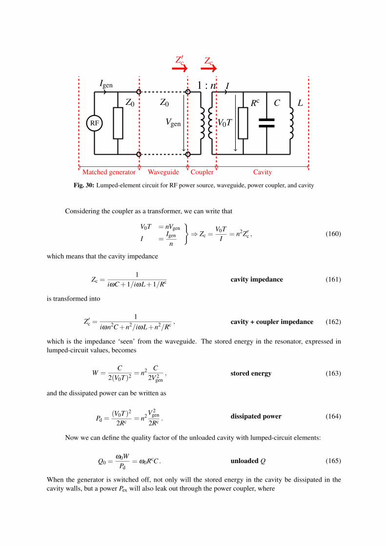
I
V0T
1 : n
Vgen
Igen
RF
Rc C LZ0 Z0
Matched generator Waveguide Coupler Cavity
Z′c Zc
Fig. 30: Lumped-element circuit for RF power source, waveguide, power coupler, and cavity
Considering the coupler as a transformer, we can write that
V0T = nVgen
I =Igen
n
⇒ Zc =
V0TI
= n2Z′c , (160)
which means that the cavity impedance
Zc =1
iωC+1/iωL+1/Rc cavity impedance (161)
is transformed into
Z′c =1
iωn2C+n2/iωL+n2/Rc , cavity + coupler impedance (162)
which is the impedance ‘seen’ from the waveguide. The stored energy in the resonator, expressed inlumped-circuit values, becomes
W =C
2(V0T )2 = n2 C2V 2
gen, stored energy (163)
and the dissipated power can be written as
Pd =(V0T )2
2Rc = n2V 2gen
2Rc .dissipated power (164)
Now we can define the quality factor of the unloaded cavity with lumped-circuit elements:
Q0 =ω0W
Pd= ω0RcC . unloaded Q (165)
When the generator is switched off, not only will the stored energy in the cavity be dissipated in thecavity walls, but a power Pex will also leak out through the power coupler, where

Pex =V 2
gen
2Z0. (166)
Using Pex, one can define the quality factor of the external load. The external Q is thus defined as
Qex =ω0WPex
= n2ω0Z0C . external Q (167)
4.8.1 Undriven cavityIn order to understand the power balance and matching for a driven cavity with beam, we start with asimple case, assuming that the RF is switched off and that there is no beam in the cavity. The powerbalance is then
Ptot = Pd +Pex ,power balance of undrivencavity (168)
with which we can define the so-called ‘loaded Q’ of the ensemble of cavity and coupler by
1Ql
=1
Qex+
1Q0
. loaded Q (169)
The coupling between the cavity and the waveguide is described by the coupling factor β , where
β =Pex
Pd=
Q0
Qex=
Rc
n2Z0. coupling factor (170)
Optimum power transfer between the cavity (+ coupler) and the waveguide takes place when the impedanceat the coupler input equals the waveguide impedance at the resonance frequency of the cavity. We knowthat the cavity impedance becomes real at resonance, which means that
Zc = Rc = n2Z′c!= n2Z0 ⇒ β = 1 . (171)
It is important to keep in mind that the ‘matching condition’ β = 1 is only valid for a cavity withoutbeam.
4.8.2 RF on, beam onOnce we take the beam loading into account, the power needed in the cavity increases and will yield adifferent value for the coupling factor β at the point of optimum power transfer. A simple way to intro-duce the beam is to treat it as an additional loss in the cavity, which can be added to the power dissipatedin the cavity walls:
Pdb = Pd +Pb .dissipated power + beampower (172)
As in the case without beam, maximum power transfer to the cavity is achieved when the input impedanceof the coupler equals the impedance of the waveguide. This condition yields zero reflection and alsoimplies that the power needed in the cavity, Pbd (for losses and beam), has to be equal to Pex as definedin Eq. (166). This means that
Pex
Pdb= 1 =
Q0b
Qex⇒ Pex
Pd= 1+
Pb
Pd, (173)

where we have introduced a quality factor Q0b for the cavity plus beam. For the matched condition, wetherefore obtain a coupling factor of
β = 1+Pb
Pd,
matched coupling factor withbeam
(174)
and the following quality factors:
Qex = Q0b =ω0W
Pb +Pd=
Q0
1+Pb/Pd=
Q0
β, external Q with beam (175)
Ql =Q0
1+β=
Q0
2+Pb/Pd. loaded Q with beam (176)
In the case of a superconducting cavity, one can generally assume that Pb Pd, which means that thecoupling factor for the matched condition can be written as
β = 1+Pb
Pd≈ Pb
Pd.
matched coupling factor forSC cavity + beam (177)
Using
Pb = IbeamV0T cosφs , (178)
we can write a simple expression for calculating the loaded and external Q values for a superconductingcavity as follows:
Ql ≈ Qex ≈Q0
Pbeam/Pd=
V0T(R/Q)Ibeam cosφs
. Ql/ex for SC cavity (179)
The results in this paragraph are summarized in Table 3.
Table 3: Definitions of Q values and coupling factors for driven and undriven cavities
Undriven cavity Driven cavity1Ql
=1
Qex+
1Q0
General β =Pex
Pd=
Q0
Qex
Ql =Q0
1+β
Pex
Pd=
Q0
Qex= 1⇒ β = 1
Pex
Pdb=
Q0b
Qex= 1⇒ β = 1+
Pb
Pd
Matched case Qex = Q0 =ω0W
PdQex = Q0b =
ω0WPd +Pb
Ql =Q0
2Ql =
Q0
2+Pb/Pd

4.9 ‘Matching’ a cavityIn the last section, it was claimed that part of an electromagnetic wave is reflected when it ‘sees’ a changein impedance during its propagation. In fact, the whole purpose of the power coupler was to transformthe impedance of the waveguide into the impedance of the cavity. In this last section, we shall see whythis is so. For this purpose, we look at a transmission line as shown in Fig. 31.
Z0
V+, V−
I+
I−
Fig. 31: Voltages and currents along a transmission line
This transmission line is representative of a waveguide, a coaxial line, or any other kind of trans-port geometry used to guide electromagnetic waves. Since waves can travel in the positive and negative zdirections, a sign convention is introduced for the associated voltages and currents, as shown in Fig. 31,where the voltage vectors of the forward and reflected waves have the same direction and the currentvectors have opposite directions.
Using the same time and location dependence as for the electric and magnetic fields in a wave-guide, we can write
V =V0ei(kz−ωt)+ΓV0ei(−kz−ωt) , (180)
I =V0
Z0ei(kz−ωt)−Γ
V0
Z0ei(−kz−ωt) , (181)
where we have introduced a reflection coefficient Γ. If we connect a cavity to an impedance Z′c at z = 0,the expressions above simplify to
V =V0e−iωt(1+Γ) , (182)
I =V0
Z0e−iωt(1−Γ) , (183)
and the cavity impedance can be expressed in terms of the transmission line impedance Z0 and thereflection coefficient Γ:
Z′c =VI= Z0
1+Γ
1−Γ. (184)
We can then rearrange the equation for the reflection coefficient and obtain
Γ =Z′c−Z0
Z′c +Z0=
1−β
1+β. (185)
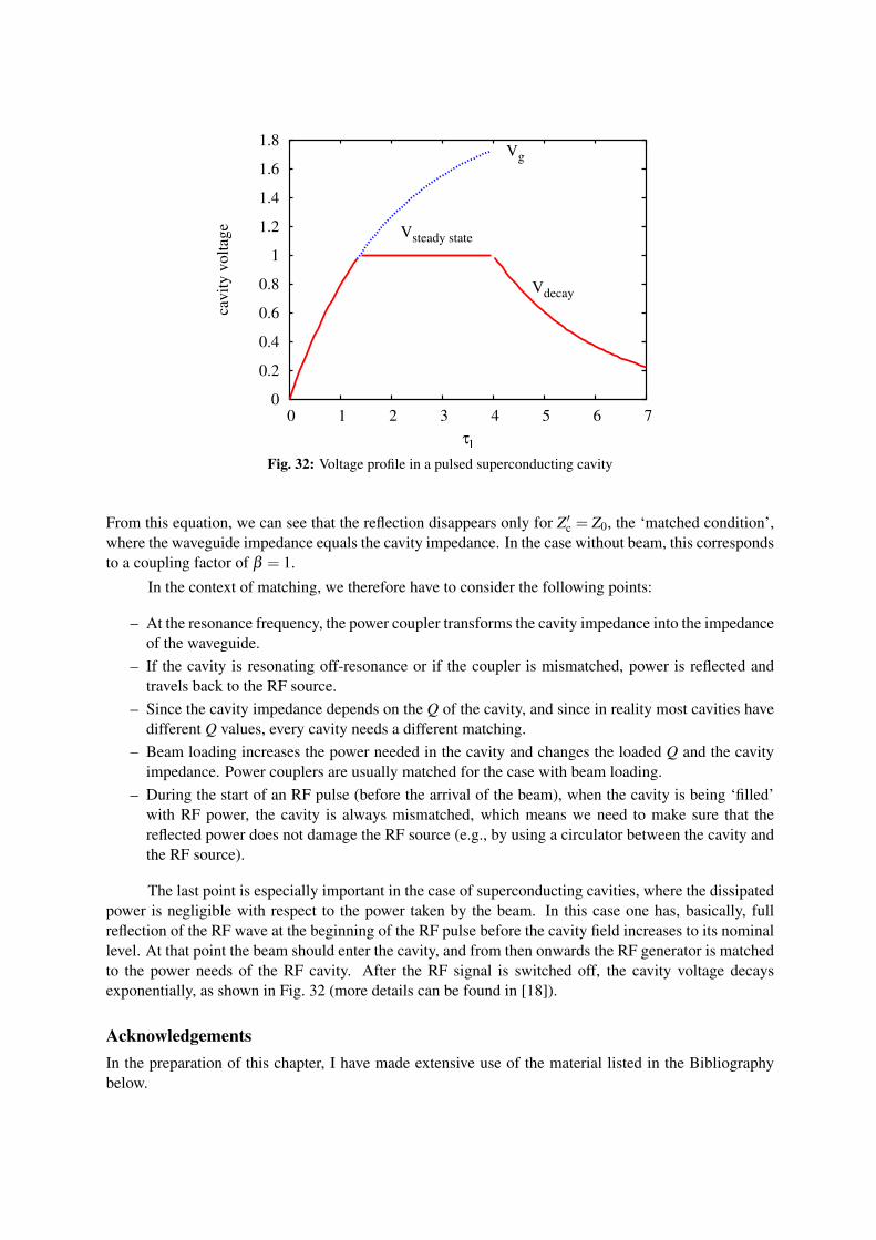
0
0.2
0.4
0.6
0.8
1
1.2
1.4
1.6
1.8
0 1 2 3 4 5 6 7
cavit
y v
olt
age
τl
Vg
Vsteady state
Vdecay
Fig. 32: Voltage profile in a pulsed superconducting cavity
From this equation, we can see that the reflection disappears only for Z′c = Z0, the ‘matched condition’,where the waveguide impedance equals the cavity impedance. In the case without beam, this correspondsto a coupling factor of β = 1.
In the context of matching, we therefore have to consider the following points:
– At the resonance frequency, the power coupler transforms the cavity impedance into the impedanceof the waveguide.
– If the cavity is resonating off-resonance or if the coupler is mismatched, power is reflected andtravels back to the RF source.
– Since the cavity impedance depends on the Q of the cavity, and since in reality most cavities havedifferent Q values, every cavity needs a different matching.
– Beam loading increases the power needed in the cavity and changes the loaded Q and the cavityimpedance. Power couplers are usually matched for the case with beam loading.
– During the start of an RF pulse (before the arrival of the beam), when the cavity is being ‘filled’with RF power, the cavity is always mismatched, which means we need to make sure that thereflected power does not damage the RF source (e.g., by using a circulator between the cavity andthe RF source).
The last point is especially important in the case of superconducting cavities, where the dissipatedpower is negligible with respect to the power taken by the beam. In this case one has, basically, fullreflection of the RF wave at the beginning of the RF pulse before the cavity field increases to its nominallevel. At that point the beam should enter the cavity, and from then onwards the RF generator is matchedto the power needs of the RF cavity. After the RF signal is switched off, the cavity voltage decaysexponentially, as shown in Fig. 32 (more details can be found in [18]).
AcknowledgementsIn the preparation of this chapter, I have made extensive use of the material listed in the Bibliographybelow.
References[1] R.P. Feynman, R.B. Leighton, and M. Sands, The Feynman Lectures on Physics, Vol. II, Mainly
Electromagnetism and Matter (California Institute of Technology, 1963).[2] H. Henke, Theoretische Elektrotechnik, German script of lectures on electrodynamics at the Tech-
nical University of Berlin (1992).[3] T. Weiland, M. Krasilnikov, R. Schuhmann, A. Skarlatos, and M. Wilke, Review of theory (I, II,
III), CAS RF Engineering, Seeheim, Germany (2005).[4] M. Abramowitz and I.A. Stegun, Handbook of Mathematical Functions (Dover Publications, New
York, 1965).[5] T. Wangler, Principles of RF Linear Accelerators (Wiley-VCH, Weinheim, 2004).[6] M. Vretenar, Low-beta structures, CAS RF School, Ebeltoft, Denmark (2010).[7] D.E. Nagle, E.A. Knapp, and B.C. Knapp, Rev. Sci. Instrum. 38 (1967) 1583.[8] S. Schriber, Characteristics of full-cell terminated RF structures: results of analogue studies,
CERN/PS/2001-067 (PP) (2001).[9] S. Schriber, Phys. Rev. ST Accel. Beams 4 (2001) 122001.
[10] The Compact Linear Collider Study, http://www.cern.ch/clic-study.[11] International Linear Collider, http://www.linearcollider.org.[12] R.H. Miller, Comparison of standing wave and travelling wave structures, LINAC86 (1986).[13] V.A. Moiseev, V.V. Paramonov, and K. Floettmann, Comparison of standing and travelling wave
operations for positron pre-accelerator in the TESLA Linear Collider, EPAC (2000).[14] F. Gerigk, Cavity types, CAS RF School, Ebeltoft, Denmark, arXiv:1111.4897v1 (2010).[15] M. Schuh, F. Gerigk, J. Tuckmantel, and C.P. Welsch, Influence of higher order modes on the beam
stability in the high power superconducting proton linac, Phys. Rev. ST Accel. Beams 14 (2011)051001.
[16] F. Gerigk, J.M. Giguet, E. Montesinos, B. Riffaud, P. Ugena Tirado, and R. Wegner, The Linac4power coupler, IPAC 2011, San Sebastian, Spain, CERN-ATS-2011-040 (2011).
[17] M. Vretenar et al., The LINAC4 project at CERN, IPAC 2011, San Sebastian, Spain, CERN-ATS-2011-041 (2011).
[18] F. Gerigk, Formulae to calculate the power consumption of the SPL SC cavities, CERN-AB-Note-2006-011-RF (2006).
Bibliography– T. Weiland, M. Krasilnikov, R. Schuhmann, A. Skarlatos, and M. Wilke, Review of theory (I, II,
III), CAS RF Engineering, Seeheim, Germany (2005).– T. Wangler, Principles of RF Linear Accelerators (Wiley-VCH, Weinheim, 2004).– A. Wolski, Theory of electromagnetic fields, CAS RF Engineering, Ebeltoft, Denmark (2010).– H. Henke, Theoretische Elektrotechnik, German script of lectures on electrodynamics at the Tech-
nical University of Berlin (1992)– H. Henke, Basic concepts I and II, CAS RF Engineering, Seeheim, Germany (2005).– K. Simonyi, Foundations of Electrical Engineering, Vol. 3 (Pergamon Press, New York, 1963).
[Hungarian edition, ElmÃl’leti villamossagtan Tankonyvkiado (Budapest, 1973); German edition,Theoretische Elektrotechnik (VEB Deutscher Verlag der Wissenschaften, 1973).]
– H. Padamsee, J. Knobloch, and T. Hays, RF Superconductivity for Accelerators (Wiley, New York,2008).

AppendicesA Cartesian coordinates (x, y, z)A.1 Differential elements
dl =
dx
dy
dz
, path element (A.1)
dV = dxdydz . volume element (A.2)
A.2 Differential operators
∇φ =
∂φ
∂x∂φ
∂y∂φ
∂ z
, gradient (A.3)
∇ ·a =∂ax
∂x+
∂ay
∂y+
∂az
∂ z, divergence (A.4)
∇×a =
∂az
∂y−
∂ay
∂ z∂ax
∂ z− ∂az
∂x∂ay
∂x− ∂ax
∂y
, curl (A.5)
∆φ =∂ 2φ
∂x2 +∂ 2φ
∂y2 +∂ 2φ
∂ z2 . Laplace (A.6)
B Cylindrical coordinates (r, φ , z)B.1 Transformations
x = r cosϕ ,
y = r sinϕ ,
z = z ,
(B.1)
with 0≤ r ≤ ∞, 0≤ ϕ ≤ 2π .
B.2 Differential elements
dl =
dr
r dϕ
dz
, path element (B.2)
dV = r dr dϕ dz . volume element (B.3)
B.3 Differential operators
∇φ =
∂φ
∂ r1r
∂φ
∂ϕ
∂φ
∂ z
, gradient (B.4)
∇ ·a =1r
∂ (rar)
∂ r+
1r
∂aϕ
∂ϕ+
∂az
∂ z, divergence (B.5)
∇×a =
1r
∂az
∂ϕ−
∂aϕ
∂ z∂ar
∂ z− ∂az
∂ r1r
(∂ (raϕ)
∂ r− ∂ar
∂ϕ
)
, curl (B.6)
∆φ =∂ 2φ
∂ r2 +1r
∂φ
∂ r+
1r2
∂ 2φ
∂ϕ2 +∂ 2φ
∂ z2 . Laplace (B.7)
C Spherical coordinates (r, ϑ , ϕ)C.1 Transformations
x = r sinϑ cosϕ ,
y = r sinϑ sinϕ ,
z = r cosϑ ,
(C.1)
with 0≤ r ≤ ∞, 0≤ ϑ ≤ π , 0≤ ϕ ≤ 2π .

C.2 Differential elements
dl =
dr
r dϑ
r sinϑ dϕ
, path element (C.2)
dV = r2 sinϑ dr dϑ dϕ . volume element (C.3)
C.3 Differential operators
∇φ =
∂φ
∂ r1r
∂φ
∂ϑ
1r sinϑ
∂φ
∂ϕ
, gradient (C.4)
∇ ·a =1r2
∂ (r2ar)
∂ r+
1r sinϑ
∂ (aϑ sinϑ)
∂ϑ+
1r sinϑ
∂aϕ
∂ϕ, divergence (C.5)
∇×a =
1r sinϑ
(∂ (aϕ sinϑ)
∂ϑ− ∂aϑ
∂ϕ
)1r
(1
sinϑ
∂ar
∂ϕ−
∂ (raϕ)
∂ r
)1r
(∂ (raϑ )
∂ r− ∂ar
∂ϑ
)
, curl (C.6)
∆φ =∂ 2φ
∂ r2 +2r
∂φ
∂ r+
1r2 sinϑ
∂
∂ϑ
(sinϑ
∂φ
∂ϑ
)+
1r2 sin2
ϑ
∂ 2φ
∂ϕ2 .
Laplace (C.7)
D Useful relationships
∇ · (a×b) = b · (∇×a)−a · (∇×b) , (D.1)
∇ · (∇×a) = 0 . (D.2)