rev 2.0 — may 2018 application note - nxp.com · select the antenna type, for example, monopole,...
TRANSCRIPT

BLE Antenna Design Guide Rev 2.0 — May 2018 Application note
Document information Info Content Keywords Micro-Strip Antenna, Metal plate antenna, Chip antenna, test procedure
Abstract This document is served as a basic antenna selection guide for the customer.

NXP Semiconductors BLE Antenna Design Guide
Please be aware that important notices concerning this document and the product(s) described herein, have been included in the section 'Legal information'.
© NXP Semiconductors N.V. 2018. All rights reserved. For more information, visit: http://www.nxp.com
Date of release: May 2018 Document identifier: UM10992
Revision history Rev Date Description
0.1 20130607 Initial release 0.2 20130709 Grammatical corrections made some text added 1.0 20150324 Reviewed and migrated to NXP template 2.0 20180509 Removed the security watermark

NXP Semiconductors BLE Antenna Design Guide
UM10992 All information provided in this document is subject to legal disclaimers. © NXP Semiconductors N.V. 2018. All rights reserved.
Application note Rev. 2.0 – May 2018 3 of 43
Contact information For more information, please visit: http://www.nxp.com
Contents Contents............................................................................ 3 1. Overview .............................................................. 4 2. Typical BLE antennas comparing ..................... 4 3. Micro-Strip Antenna ........................................... 5 3.1 Overview ...................................................................... 5 3.1 Design steps ...................................................... 6 3.2 Some examples of micro-strip antenna ............. 6 3.2.1 Micro-strip “L” antenna ...................................... 6 3.2.2 Micro-strip bow-shaped antenna ....................... 9 3.2.3 Micro-strip circularly polarized antenna ............12 3.2.4 Micro-strip inverted-F antenna ..........................15 4. Metal plate antenna ...........................................21 4.1 Overview ..........................................................21 4.2 Some examples of this antenna .......................22 4.2.1 Metal plate antenna applied in NEURON project22 4.2.2 Metal plate antenna used in iCoin project .........27 5. Chip antenna ......................................................31 5.1 List of chip antenna suppliers ...........................31 5.2 Some of typical products by these suppliers ....32 5.3 Placement of chip antenna on PCB ..................35 6. Test Procedure for antenna ..............................36 6.1 Network analyzer calibration ............................37 6.2 Measurement of antenna Return Loss, Impedance and Bandwidth 37 6.3 Description of the measurement result .............38 6.4 How to design matching net for antenna ..........39 7. Legal information ...............................................41 7.1 Definitions .........................................................41 7.2 Disclaimers .......................................................41 7.3 Trademarks ......................................................41 8. List of figures .....................................................42 9. List of tables ......................................................43

NXP Semiconductors BLE Antenna Design Guide
UM10992 All information provided in this document is subject to legal disclaimers. © NXP Semiconductors N.V. 2018. All rights reserved.
Application note Rev. 2.0 — May 2018 4 of 43
1. Overview The following document serves as a basic antenna selection guide for the
customer. Various antennas are showcased and insight on their dimension,
design process, radio frequency performance, PCB layout, etc. is provided. This
is to allow the customer to select an appropriate antenna for their application.
Detailed design questions or concerns should be communicated to the FAE at
NXP.
A small description with regards to Antenna test procedure is also presented.
Some of the Antenna’s discussed in this note may require more detailed
simulation depending on the actual application. From the types of Antenna’s
discussed, chip antenna’s have the smallest footprint but are low on efficiency,
similarly microstrip antenna’s are cheap but are tedious in design and the metal
antenna’s have high efficiency. In order to guide the customer a few Antenna
suppliers are mentioned, so that customers can also have option of directly
buying from them.
For the Antenna’s described in this note, 50 Ohm input impedance has been
considered along with Omni-directional radiation pattern with a center frequency
of 2.45GHz.
2. Typical BLE antennas comparing The Following table shows the three antenna types that will be briefly discussed
in this app note. A very basic comparison of key parameters has been shown as
well. This chart helps the customer to qualify a specific antenna type for their
application.
Table 1 Typical BLE antennas comparing
Micro-strip antenna
Metal plate antenna Chip antenna
Efficiency Moderate High Low

NXP Semiconductors BLE Antenna Design Guide
UM10992 All information provided in this document is subject to legal disclaimers. © NXP Semiconductors N.V. 2018. All rights reserved.
Application note Rev. 2.0 — May 2018 5 of 43
Cost Low High Moderate
Bandwidth High Low Moderate
Average Gain Moderate High Low
Dimension Moderate High Low
Typical Applications
Sports, fitness, healthcare, medical, remote control
Sports, fitness, healthcare, medical, remote control
Sports, fitness, healthcare, medical, remote control
Polarization Linear linear Linear
Power Handling Low high Medium
Typical Impedance 50ohm 50ohm 50ohm
3. Micro-Strip Antenna
3.1 Overview The Micro-Strip antenna is one of the most popular antennas, because of its low
cost and ease of production. With the help of advanced simulation tools such as
HFSS, Microwave Office and ADS, it has become easier to design and develop
such antennas. The micro-strip antenna can also be seen as a simple fracture
antenna due to its flexible appearance. The micro-strip antenna RF performance
is highly depended on the size of the reference ground. Therefore, changing the
default reference ground size, the antenna RF characteristic including the
resonance frequency, port input impedance, etc, will change as well.
The micro-strip antenna can be designed as a circular polarized antenna. One
example will be illustrated in this document, such a design may occupy more
PCB area compared to other typical micro-strip antennas.

NXP Semiconductors BLE Antenna Design Guide
UM10992 All information provided in this document is subject to legal disclaimers. © NXP Semiconductors N.V. 2018. All rights reserved.
Application note Rev. 2.0 — May 2018 6 of 43
Micro-strip antennas can be designed into antenna arrays to get high antenna
gain, which is not used widely in the consumer electronics products due to the
increased PCB size.
3.1 Design steps Following are some basic steps required to bring up the design.
◆Select the antenna type, for example, monopole, dipole or IFA antenna;
◆Roughly calculate the antenna dimension using the experience formula;
◆Set up the simulation module using simulation tools, such as, HFSS, ADS;
◆Simulate and adjust the antenna dimension till the simulation result meets
the requirement;
The third step is the most critical. If the antenna model is not correct or has
significant error, caused by incorrect parameters or module structure, the
simulation result may be incorrect. S11, bandwidth, input impedance, gain, cross
polarization and axial ratio are the determining parameters for the antenna
performance.
3.2 Some examples of micro-strip antenna 3.2.1 Micro-strip “L” antenna
As a micro-strip antenna, the L shaped antenna is the simplest solution. Its
resonance frequency is related with the antenna line width “w”, the antenna
length “L”, the dimension and the dielectric constant of the substrate. Shown
below is an example of such a design. The dielectric constant for the FR4
substrate is 4.4, the thickness is 0.5mm. Following figure shows the dimension
and layout of the antenna.
Figure 1 “L” antenna dimension
NXP Semiconductors BLE Antenna Design Guide
UM10992 All information provided in this document is subject to legal disclaimers. © NXP Semiconductors N.V. 2018. All rights reserved.
Application note Rev. 2.0 — May 2018 7 of 43
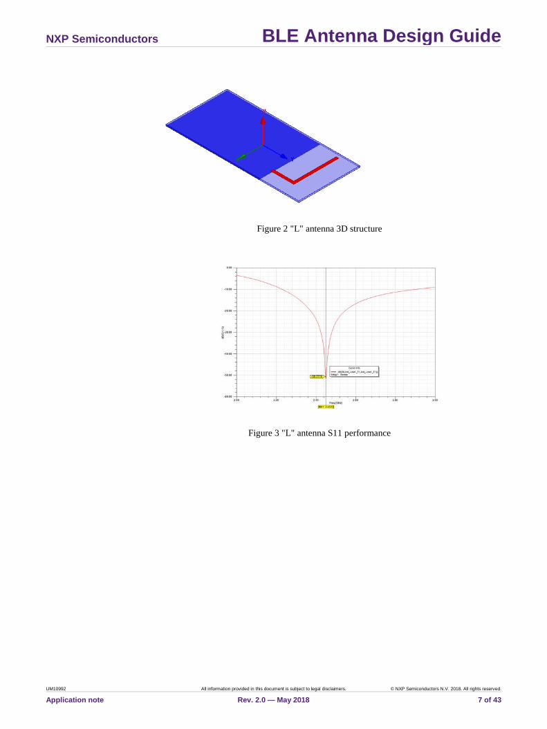
Figure 2 "L" antenna 3D structure
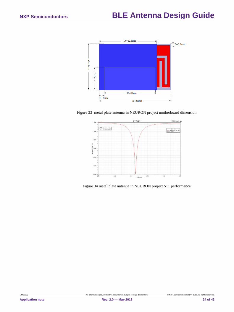
Figure 3 "L" antenna S11 performance

NXP Semiconductors BLE Antenna Design Guide
UM10992 All information provided in this document is subject to legal disclaimers. © NXP Semiconductors N.V. 2018. All rights reserved.
Application note Rev. 2.0 — May 2018 8 of 43
Figure 4 "L"antenna Smith chart
Figure 5 "L" antenna EH plane gain characteristic
Figure 6 "L" antenna 3D radiation pattern

NXP Semiconductors BLE Antenna Design Guide
UM10992 All information provided in this document is subject to legal disclaimers. © NXP Semiconductors N.V. 2018. All rights reserved.
Application note Rev. 2.0 — May 2018 9 of 43
Table 2 Effect on performance when critical dimensions are altered
Antenna Dimension
Change Parameter Effect
w Increase
Resonance frequency Increase
Bandwidth Becomes wide
Decrease Resonance frequency Decrease
Bandwidth Becomes narrow
L Increase
Resonance frequency Decrease
Bandwidth Becomes narrow
Decrease Resonance frequency Increase
Bandwidth Becomes wide
E Increase
Resonance frequency Decrease
Bandwidth Becomes wide
Decrease Resonance frequency Increase
Bandwidth Becomes narrow
3.2.2 Micro-strip bow-shaped antenna This is another widely used monopole antenna. Its resonance frequency is in
correspondence with the antenna line width “w”, the line gap “D”, the line length
“L”, and dielectric constant of the substrate. FR4 with a dielectric constant of
about 4.4 is used in the following illustration. In order to get better radiation
efficiency it is advised that the area without the reference ground copper be
enlarged.
Figure 7 Bow shaped antenna dimension

NXP Semiconductors BLE Antenna Design Guide
UM10992 All information provided in this document is subject to legal disclaimers. © NXP Semiconductors N.V. 2018. All rights reserved.
Application note Rev. 2.0 — May 2018 10 of 43
Figure 8 Bow shaped antenna3D structure
Figure 9 Bow shaped antenna S11 performance
Figure 10 Bow shaped antenna Smith chart

NXP Semiconductors BLE Antenna Design Guide
UM10992 All information provided in this document is subject to legal disclaimers. © NXP Semiconductors N.V. 2018. All rights reserved.
Application note Rev. 2.0 — May 2018 11 of 43
Figure 11 Bow shaped antenna EH plane gain characteristic
Figure 12 Bow shaped antenna 3D radiation pattern
Table 3 Effect on performance when critical dimensions are altered
Antenna Dimension
Change Parameter Effect
w Increase
Resonance frequency Increase
Bandwidth Becomes wide
Decrease Resonance frequency Decrease
Bandwidth Becomes narrow
L Increase Resonance frequency Decrease
Bandwidth Becomes narrow

NXP Semiconductors BLE Antenna Design Guide
UM10992 All information provided in this document is subject to legal disclaimers. © NXP Semiconductors N.V. 2018. All rights reserved.
Application note Rev. 2.0 — May 2018 12 of 43
Decrease Resonance frequency Increase
Bandwidth Becomes wide
D Increase
Resonance frequency Decrease
Bandwidth Becomes narrow
Decrease Resonance frequency Increase
Bandwidth Becomes wide
E Increase
Resonance frequency Decrease
Bandwidth Becomes wide
Decrease Resonance frequency Increase
Bandwidth Becomes narrow
3.2.3 Micro-strip circularly polarized antenna One of the popular micro-strip antennas is the circularly polarized configuration.
The PCB area required to implement such an antenna is comparatively larger
than linear polarized antenna, but the antenna receive performance is better.
The theory of realizing circular polarization requires two linear polarization
electric field vectors simultaneously; both of the vectors must be orthotropic and
have 90º phase difference between them. One important parameter for this
antenna is the axial ratio, which is required to be lower than 3dB. There are
many ways to realize circular polarization micro-strip antenna. The following is
one example.
Figure 13 circularly polarized antenna structure

NXP Semiconductors BLE Antenna Design Guide
UM10992 All information provided in this document is subject to legal disclaimers. © NXP Semiconductors N.V. 2018. All rights reserved.
Application note Rev. 2.0 — May 2018 13 of 43
Figure 14 circularly polarized antenna dimension
Figure 15 circularly polarized antenna 3D structure
Figure 16 circularly polarized antenna S11 performance

NXP Semiconductors BLE Antenna Design Guide
UM10992 All information provided in this document is subject to legal disclaimers. © NXP Semiconductors N.V. 2018. All rights reserved.
Application note Rev. 2.0 — May 2018 14 of 43
Figure 17 circularly polarized antenna Smith chart
Figure 18 circularly polarized antenna axial ratio characteristic (1)
Figure 19 circularly polarized antenna axial ratio characteristic (2)

NXP Semiconductors BLE Antenna Design Guide
UM10992 All information provided in this document is subject to legal disclaimers. © NXP Semiconductors N.V. 2018. All rights reserved.
Application note Rev. 2.0 — May 2018 15 of 43
3.2.4 Micro-strip inverted-F antenna The inverted-F antenna is easy to design, and quiet popularly used in various
BLE applications, such as USB dongles, Proximity, heart rate monitor (HRM),
human interface device (HID) etc. The IFA antenna is used widely due to its
excellent performance and small size, therefore it has been described in detail.
Following figure illustrates the structure of a simple inverted-F antenna. The
expected resonance frequency of this antenna is 2.44G.
Figure 20 IFA antenna dimension
Figure 21 IFA antenna 3D structure
While laying out the IFA PCB attention to some key features is required:

NXP Semiconductors BLE Antenna Design Guide
UM10992 All information provided in this document is subject to legal disclaimers. © NXP Semiconductors N.V. 2018. All rights reserved.
Application note Rev. 2.0 — May 2018 16 of 43
1. The feed arm should be fed with a 50ohm CPWG transmission line. The length of the
transmission line should be as short as possible. The transmission line can be
covered by mask.
2. The short arm should be connected to the reference ground plane with at least 2 vias.
3. The ground plane under the antenna should be removed.
4. The solder-mask plane on and under the antenna should be added.
5. The ground plane on the different layers should be connected together by vias along
the ground plane edge.
6. The dimension of the ground plane is as important as the antenna dimension itself.
7. The layout of the matching net should not alter the impedance of transmission line.
8. One “T” or pie matching net is generally enough for all kinds of antennas. The
matching net should be as simple as possible.
If there is a change in the dimensions of the substrate, the antenna dimension
should also be changed. Any change to the dimension marked in Figure above
may change the antenna RF performance including resonance frequency and
input impedance. The changes should be based on the simulation result. It is
recommended to use simulation tool to design and debug the antenna. The
antenna position dimension is also very important for the antenna design. As
shown in Figure above, the position dimension is “T”.
Figure 22 IFA antenna PCB layout
We usually use CPWG (Coplanar waveguide) as the feed line for the antenna.
The characteristic impedance of the CPWG should equal the input impedance of
the antenna; in order to improve the return loss at the antenna input port 50ohm
input impedance is used as a standard. It is not recommended to use the micro-
strip line as the feed line because it will change the antenna’s effective electric

NXP Semiconductors BLE Antenna Design Guide
UM10992 All information provided in this document is subject to legal disclaimers. © NXP Semiconductors N.V. 2018. All rights reserved.
Application note Rev. 2.0 — May 2018 17 of 43
length. Around the ground plane small vias connected to ground should be
placed, such that their diameter is between 8 to 10 mils.
The matching net should not be removed even if the impedance match between
the feed line and antenna is optimum. In order to avoid errors due to
unpredictable issues, such as manufacturing error, dielectric constant error, etc.,
the matching net should always be present between the feed line and the
antenna. Generally, one T or π matching net is enough for most of antenna
applications. The component pad size of the matching net should be suitable for
the feed line dimension. The matching net design in Figure 2 can be seen as a
reference design.
The inverted-F antenna metal should be open to air, with nothing covering it. If
not, it will restrain the surface wave generation. In addition, the substrate on the
inverted-F antenna area should not have any mask.
The inverted-F antenna performance can be affected by many factors, like the
PCB board size, the substrate dielectric constant, the antenna size, and the
antenna position on PCB board. The following section shows how these
parameters affect the antenna performance.

NXP Semiconductors BLE Antenna Design Guide
UM10992 All information provided in this document is subject to legal disclaimers. © NXP Semiconductors N.V. 2018. All rights reserved.
Application note Rev. 2.0 — May 2018 18 of 43
Figure 23 IFA antenna S11 performance
Figure 24 IFA antenna Smith chart

NXP Semiconductors BLE Antenna Design Guide
UM10992 All information provided in this document is subject to legal disclaimers. © NXP Semiconductors N.V. 2018. All rights reserved.
Application note Rev. 2.0 — May 2018 19 of 43
Figure 25 IFA antenna EH plane gain characteristic
Figure 26 IFA antenna 3D radiation pattern
Figure 27 IFA antenna axial ratio performance

NXP Semiconductors BLE Antenna Design Guide
UM10992 All information provided in this document is subject to legal disclaimers. © NXP Semiconductors N.V. 2018. All rights reserved.
Application note Rev. 2.0 — May 2018 20 of 43
Figure 28 IFA antenna current amplitude distribution
Table 4 Effect on performance when critical parameters are altered
Antenna dimension
change parameter effect
e Increase Resonance frequency Decrease
Bandwidth Becomes wide
Decrease Resonance frequency Increase
Bandwidth Becomes narrow
f Increase Resonance frequency Decrease
Bandwidth Becomes narrow
Decrease Resonance frequency Increase
Bandwidth Becomes wide
g Increase Resonance frequency Increase
Bandwidth Becomes wide
Decrease Resonance frequency Decrease
Bandwidth Becomes narrow
b Increase Resonance frequency Decrease
Bandwidth Becomes wide
Decrease Resonance frequency Increase
Bandwidth Becomes narrow
Sub_H Increase Resonance frequency Decrease
Bandwidth Becomes narrow

NXP Semiconductors BLE Antenna Design Guide
UM10992 All information provided in this document is subject to legal disclaimers. © NXP Semiconductors N.V. 2018. All rights reserved.
Application note Rev. 2.0 — May 2018 21 of 43
4. Metal plate antenna
4.1 Overview The metal plate antenna is a high efficiency, high power handling antenna
solution used widely for various 2.4GHz application solutions such as fitness,
healthcare, medical, remote control, etc. It can be designed to monopole, dipole
and IFA antennas, but is usually designed as IFA to reduce the antenna size. In
addition, its performance including bandwidth characteristic is much depended
on the dimension of the PCB board. Larger
Decrease Resonance frequency Increase
Bandwidth Becomes wide
T Increase Resonance frequency Increase
Bandwidth Becomes wide
Decrease Resonance frequency Decrease
Bandwidth Becomes narrow
h Increase Resonance frequency Decrease
Bandwidth Becomes narrow
Decrease Resonance frequency Increase
Bandwidth Becomes wide
a Increase Resonance frequency Decrease
Bandwidth Becomes narrow
Decrease Resonance frequency Increase
Bandwidth Becomes wide
w Increase Resonance frequency Decrease
Bandwidth Becomes wide
Decrease Resonance frequency Increase
Bandwidth Becomes narrow
ε(dielectric
constant of
the
substrate)
Increase Resonance frequency Decrease
Bandwidth Becomes narrow
Decrease Resonance frequency Increase
Bandwidth Becomes wide

NXP Semiconductors BLE Antenna Design Guide
UM10992 All information provided in this document is subject to legal disclaimers. © NXP Semiconductors N.V. 2018. All rights reserved.
Application note Rev. 2.0 — May 2018 22 of 43
PCB board means a wider antenna bandwidth. Following is an example of the
metal plate antenna.
Figure 29 Metal plate antenna 3D structure
In this figure, the red part is the metal plate antenna, and it is an IFA antenna.
The gray area is the clearance space of the PCB board. The antenna is usually
made of stainless steel and its default thickness is about 0.15 millimeters. The
design steps are similar to that of the micro-strip antenna.
4.2 Some examples of this antenna In section provides some antenna examples, most of the designs have been
verified by end customers and have been incorporated in their solutions.
4.2.1 Metal plate antenna applied in NEURON project This metal plate antenna is also made of stainless steel and its default thickness
is about 0.15mm, the substrate is made of FR4 and its dielectric constant is
about 4.4. The following is the 3D structure of the antenna.
Figure 30 metal plate antenna in NEURON project 3D structure
In this figure, the red part is the metal plate antenna and the gray area is the
cleared space on the PCB. The PCB board structure module is completely

NXP Semiconductors BLE Antenna Design Guide
UM10992 All information provided in this document is subject to legal disclaimers. © NXP Semiconductors N.V. 2018. All rights reserved.
Application note Rev. 2.0 — May 2018 23 of 43
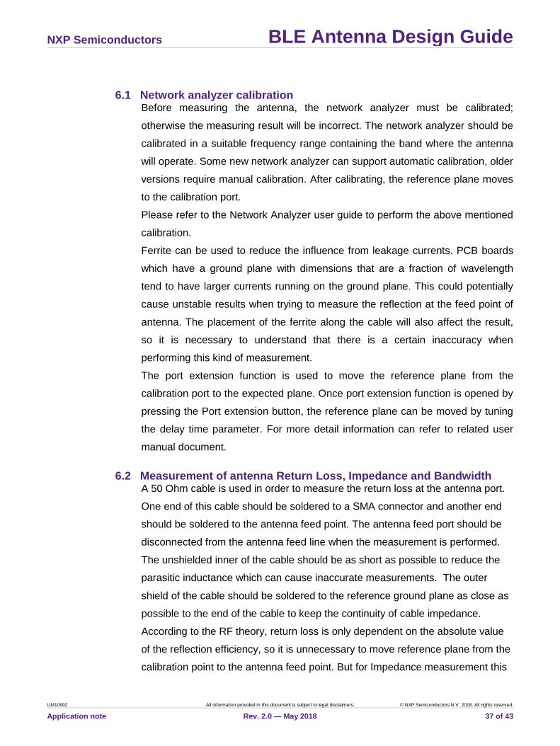
compatible with the real PCB board. The dimension of this antenna is illustrated
in the following figure. The position of the antenna on the PCB board marked “E”
in the following figure is also very important and its value can affect the antenna
resonance frequency.
Figure 31 metal plate antenna in NEURON project dimension(1)
Figure 32 metal plate antenna in NEURON project dimension (2)
The dimension of the PCB board is illustrated in the following figure.
NXP Semiconductors BLE Antenna Design Guide
UM10992 All information provided in this document is subject to legal disclaimers. © NXP Semiconductors N.V. 2018. All rights reserved.
Application note Rev. 2.0 — May 2018 24 of 43
Figure 33 metal plate antenna in NEURON project motherboard dimension
Figure 34 metal plate antenna in NEURON project S11 performance

NXP Semiconductors BLE Antenna Design Guide
UM10992 All information provided in this document is subject to legal disclaimers. © NXP Semiconductors N.V. 2018. All rights reserved.
Application note Rev. 2.0 — May 2018 25 of 43
Figure 35 metal plate antenna in NEURON project Smith chart
Figure 36 metal plate antenna in NEURON project input impedance characteristic
Figure 37 metal plate antenna in NEURON project EH plane gain characteristic

NXP Semiconductors BLE Antenna Design Guide
UM10992 All information provided in this document is subject to legal disclaimers. © NXP Semiconductors N.V. 2018. All rights reserved.
Application note Rev. 2.0 — May 2018 26 of 43
Figure 38 metal plate antenna in NEURON project 3D radiation pattern
Table 5 Effect on performance when critical parameters are altered
Antenna dimension
Change parameter effect
a Increase Resonance frequency Decrease
Bandwidth Becomes narrow
Decrease Resonance frequency Increase
Bandwidth Becomes wide
b Increase Resonance frequency Increase
Bandwidth Becomes wide
Decrease Resonance frequency Decrease
Bandwidth Becomes narrow
c Increase Resonance frequency Decrease
Bandwidth Becomes narrow
Decrease Resonance frequency Increase
Bandwidth Becomes wide
e Increase Resonance frequency Decrease
Bandwidth Becomes narrow
Decrease Resonance frequency Increase
Bandwidth Becomes wide
k Increase Resonance frequency Increase
Bandwidth Becomes wide
Decrease Resonance frequency Decrease

NXP Semiconductors BLE Antenna Design Guide
UM10992 All information provided in this document is subject to legal disclaimers. © NXP Semiconductors N.V. 2018. All rights reserved.
Application note Rev. 2.0 — May 2018 27 of 43
Bandwidth Becomes narrow
E Increase Resonance frequency Increase
Bandwidth Becomes wide
Decrease Resonance frequency Decrease
Bandwidth Becomes narrow
4.2.2 Metal plate antenna used in iCoin project The antenna was used in the iCoin project, which is also made of stainless steel
and the default thickness is about 0.15mm. This antenna shows better radiation
performance during field test compared with the micro-strip antenna and chip
antenna in the same conditions. The following figure illustrates the antenna’s 3D
structure. The red part is the metal plate antenna and the pea green area is the
clearance area on the PCB.
Figure 39 metal plate in iCoin project 3D structure
This antenna is also a kind of IFA .Its resonance frequency and radiation
performance is not only dependant on its dimension but also that of the PCB. As
mentioned in the previous part of this document, the clearance area is critical to
the design. It is strongly recommended that a significant clearance space is used
in the design. The following figure shows the dimensions of the antenna.

NXP Semiconductors BLE Antenna Design Guide
UM10992 All information provided in this document is subject to legal disclaimers. © NXP Semiconductors N.V. 2018. All rights reserved.
Application note Rev. 2.0 — May 2018 28 of 43
Figure 40 metal plate in iCoin project dimension (1)
Figure 41 metal plate in iCoin project dimension (2)
Figure 42 metal plate in iCoin project motherboard dimension
In this figure, the antenna is shown to be transparent in order to mark the
cleaning space area dimension conveniently.

NXP Semiconductors BLE Antenna Design Guide
UM10992 All information provided in this document is subject to legal disclaimers. © NXP Semiconductors N.V. 2018. All rights reserved.
Application note Rev. 2.0 — May 2018 29 of 43
Figure 43 metal plate in iCoin project S11 performance
Figure 44 metal plate in iCoin project Smith chart
Figure 45 metal plate in iCoin project EH plane gain characteristic

NXP Semiconductors BLE Antenna Design Guide
UM10992 All information provided in this document is subject to legal disclaimers. © NXP Semiconductors N.V. 2018. All rights reserved.
Application note Rev. 2.0 — May 2018 30 of 43
Figure 46 metal plate in iCoin project 3D radiation pattern
Table 6 Effect on performance when critical parameters are altered
Antenna dimension
change parameter effect
a Increase Resonance frequency Decrease
Bandwidth Becomes narrow
Decrease Resonance frequency Increase
Bandwidth Becomes wide
b Increase Resonance frequency Unchanged
Bandwidth Becomes narrow
Decrease Resonance frequency Unchanged
Bandwidth Becomes wide
c Increase Resonance frequency Increase
Bandwidth Becomes narrow
Decrease Resonance frequency Decrease
Bandwidth Becomes wide
d Increase Resonance frequency Decrease
Bandwidth Becomes narrow
Decrease Resonance frequency Increase
Bandwidth Becomes wide
s Increase Resonance frequency Unchanged
Bandwidth Becomes wide
Decrease Resonance frequency Unchanged

NXP Semiconductors BLE Antenna Design Guide
UM10992 All information provided in this document is subject to legal disclaimers. © NXP Semiconductors N.V. 2018. All rights reserved.
Application note Rev. 2.0 — May 2018 31 of 43
Bandwidth Becomes narrow
r Increase Resonance frequency Decrease
Bandwidth Becomes wide
Decrease Resonance frequency Increase
Bandwidth Becomes narrow
θ Increase Resonance frequency Increase
Bandwidth Becomes wide
Decrease Resonance frequency Decrease
Bandwidth Becomes narrow
5. Chip antenna Chip antenna is usually supplied by professional manufacturer and is applied
very conveniently by the users. With some key features such as very small size,
lower cost and ease of use, chip antenna is widely used in various wireless
applications, such as, WIFI, Bluetooth, etc. In the application process, the user is
required to design good feed line, matching net and PCB structure to meet chip
antenna performance requirement. The manufacturer often supplies chip
antenna application note document as a reference for the user. In this section,
some antenna vendors along with their product part numbers are presented for
easy reference.
5.1 List of chip antenna suppliers
Table 7 chip antenna supplier list
Supplier Test Main 2.4G chip antenna products
Y AN3216, AN2051, AN6520, AN0835, AN9520
Y RFANT5220110AT,RFANT3216120AT,RFECA3216060A1T,RGANT8010100A0T,RFGFRA9937380A3T,RGFRA1903041A1T
Y BTCA5020,BTCA4020,BTCA1206,BTCA0805
N KTDA72-2R470G-S1, KTDA31-2R470G-S1, KTDA22-2R470G-S1, KTDA21-2R470G-S1,

NXP Semiconductors BLE Antenna Design Guide
UM10992 All information provided in this document is subject to legal disclaimers. © NXP Semiconductors N.V. 2018. All rights reserved.
Application note Rev. 2.0 — May 2018 32 of 43
Y 2450AT18B100,2450AT18A100,2450AT18D0100,2450AT18E0100,2450AT43D100,2450AT43H0100,2450AT45A100
Y A10192,A5839,A5645,A6111,A6150,A10381
N W3001,W3008,W3008C,W3108
N FR05-S1-N-0-001,FR05-S1-N-0-104,FR05-S1-N-0-102,FR05-S1-N-0-110
5.2 Some of typical products by these suppliers
Table 8 RAINSUN chip antenna product list
Part number
AN3216 AN2051 AN6520 AN0835 AN9520
Size 3.2mm (L)x 1.6mm(W) x 1.04mm(H)
5.05mm (L)x 2.0mm(W) x 1.07mm(H)
6.5mm (L)x 2.2mm(W) x 1.0mm(H)
8.0mm (L)x 3.5mm(W) x 1.0mm(H)
9.5mm (L)x 2.1mm(W) x 1.0mm(H)
Center frequency
2.45GHz 2.45GHz 2.45GHz 2.45GHz 2.45GHz
Peak gain 0.5dBi(typ.) 0.5dBi(typ.) 0.5dBi(typ.) 1dBi(typ.) 1.5dBi(typ.)
Operation temperature
-40~+85℃ -40~+85℃ -40~+85℃ -40~+85℃ -40~+85℃
Storage temperature
-40~+85℃ -40~+85℃ -40~+85℃ -40~+85℃ -40~+85℃
VSWR 2.5(max) 2.5(max) 2.5(max) 2(max) 2(max)
Input impedance
50Ω 50Ω 50Ω 50Ω 50Ω
Power handling
1W 2W 1W 3W 3W
Bandwidth 110MHz(typ.) 110MHz(typ.) 110MHz(typ.) 180MHz(typ.) 200MHz(typ.)
Azimuth beam width
Omni-directional
Omni-directional
Omni-directional
Omni-directional
Omni-directional
polarization linear linear linear linear linear

NXP Semiconductors BLE Antenna Design Guide
UM10992 All information provided in this document is subject to legal disclaimers. © NXP Semiconductors N.V. 2018. All rights reserved.
Application note Rev. 2.0 — May 2018 33 of 43
Table 9 PSA chip antenna product list
Part number
RFANT5220110AT
RFECA3216060A1T
RGANT8010100A0T
RFGFRA9937380A3T
Size 5.2mm(L) x 2.0mm(W) x 1.1mm(H)
3.2mm(L) x 1.6mm(W) x 0.6mm(H)
8.0mm(L) x 1.0mm(W) x 1.0mm(H)
9.9mm(L) x 3.7mm(W) x 3.8mm(H)
Frequency range
2.4~2.5GHz 2.4G~2.835GHz 2.4~2.5GHz 2.4~2.5GHz
gain 2dBi(typ.) 2dBi(typ.) 2dBi(typ.) 2dBi(typ.)
VSWR 2(max) 2(max) 2(max) 2(max)
polarization
linear linear linear linear
Azimuth beam width
Omni-directional
Omni-directional Omni-directional Omni-directional
Input impedance
50Ω 50Ω 50Ω 50Ω
Rated Power
3W 2W 1W
Maximum input power
5W for 5 minutes
5W for 5 minutes 5W for 5 minutes
Table 10 CHENGDIAN electronic chip antenna product list
Part number
BTCA5020 BTCA4020 BTCA1206 BTCA0805
Size 5.0mm(L) x 2.0mm(W) x 0.5mm (H)
4.0mm(L) x 2.0mm(W) x 1.2mm (H)
3.0mm(L) x 1.5mm(W) x 0.9mm (H)
2.0mm(L) x 1.2mm(W) x 0.85mm (H)
Center frequency
2.45GHz 2.45GHz 2.45GHz 2.45GHz
Peak gain 2dBi(typ.) 2dBi(typ.) 2dBi(typ.) 1dBi(typ.)
VSWR 2 2 2 2
Input impedance
50Ω 50Ω 50Ω 50Ω
Azimuth beam width
Omni-directional
Omni-directional
Omni-directional
Omni-directional
polarization linear linear linear linear

NXP Semiconductors BLE Antenna Design Guide
UM10992 All information provided in this document is subject to legal disclaimers. © NXP Semiconductors N.V. 2018. All rights reserved.
Application note Rev. 2.0 — May 2018 34 of 43
Table 11 JOHANSON chip antenna product list
Part number
2450AT18B100
2450AT18A100
2450AT18D0100
2450AT18E0100
2450AT43D100
Size 3.2mm (L)x 1.6mm(W) x 1.3mm(H)
3.2mm (L)x 1.6mm(W) x 1.3mm(H)
3.2mm (L)x 1.6mm(W) x 1.2mm(H)
3.2mm (L)x 1.6mm(W) x 1.2mm(H)
6.0mm (L)x 2.5mm(W) x 2.0mm(H)
Center frequency
2.45GHz 2.45GHz 2.45GHz 2.45GHz 2.45GHz
Peak gain 0.5dBi(typ.) 0.5dBi(typ.) 1.5dBi(typ.)
1.0dBi(typ.) -0.5dBi(typ.)
Average gain
-0.5dBi(typ.) -0.5dBi(typ.) -1.0dBi(typ.)
-3.0dBi(typ.) -3.6dBi(typ.)
Operation temperature
-40~+85℃ -40~+85℃ -40~+85℃
-40~+85℃ -40~+85℃
Storage temperature
-40~+85℃ -40~+85℃ -40~+85℃
-40~+85℃ -40~+85℃
Return Loss
9.5dB(min) 9.5dB (min) 6dB(min) 4.4dB (min) 9.5dB (min)
Input impedance
50Ω 50Ω 50Ω 50Ω 50Ω
Power handling
3W(max) 3W(max) 2W(max) 2W max 3W max
Bandwidth
100MHz(typ.) 100MHz(typ.) 100MHz(typ.)
100MHz(typ.)
100MHz(typ.)
polarization
linear linear linear linear linear
Table 12 ANTENOVA chip antenna product list
Part number
A10192 A5839 A5645 A6111 A6150
Size 4.0mm(L) x 3.0mm(W) x 1.1mm(H)
12.8mm(L) x 3.9mm(W) x 1.1mm(H)
20.5mm(L) x 3.6mm(W) x 3.3mm(H)
12.8mm(L) x 3.6mm(W) x 3.3mm(H)
6.1mm(L) x 3.9mm(W) x 1.1mm(H)
Frequency range
2.4~2.5GHz 2.4~2.5GHz 2.4~2.5GHz 2.4~2.5GHz 2.4~2.5GHz
efficiency 65% 75% 65% 45% 65%
Peak gain 0.8dBi 2.1dBi - - -
Average gain
-1.9dBi -1.2dBi - - -

NXP Semiconductors BLE Antenna Design Guide
UM10992 All information provided in this document is subject to legal disclaimers. © NXP Semiconductors N.V. 2018. All rights reserved.
Application note Rev. 2.0 — May 2018 35 of 43
Radiation pattern
Omni-directional
Omni-directional
Omni-directional
Omni-directional
Omni-directional
VSWR 2(max) 1.8(max) 1.8(max) 2.3(max) 1.9(max)
Input impedance
50Ω 50Ω 50Ω 50Ω 50Ω
polarization linear linear linear linear linear
5.3 Placement of chip antenna on PCB How to layout the chip antenna on the PCB is a very important. The antenna
position on PCB board, the size of cleaning space area and the distance
between the antenna and reference ground plane will affect the antenna
resonance frequency and impedance. In this part, some typical solutions will be
described.

NXP Semiconductors BLE Antenna Design Guide
UM10992 All information provided in this document is subject to legal disclaimers. © NXP Semiconductors N.V. 2018. All rights reserved.
Application note Rev. 2.0 — May 2018 36 of 43
Figure 47 excellent cases for chip antenna placement
Figure 48 good and acceptable cases for chip antenna placement
Figure 49 not-recommended cases for chip antenna placement
6. Test Procedure for antenna In this section, the 2.4GHz antenna test procedure will be introduced. Antenna
test procedure including network analyzer calibration, RL(return loss)
measurement, input impedance measurement, and bandwidth measurement.
NXP Semiconductors BLE Antenna Design Guide
UM10992 All information provided in this document is subject to legal disclaimers. © NXP Semiconductors N.V. 2018. All rights reserved.
Application note Rev. 2.0 — May 2018 37 of 43
6.1 Network analyzer calibration Before measuring the antenna, the network analyzer must be calibrated;
otherwise the measuring result will be incorrect. The network analyzer should be
calibrated in a suitable frequency range containing the band where the antenna
will operate. Some new network analyzer can support automatic calibration, older
versions require manual calibration. After calibrating, the reference plane moves
to the calibration port.
Please refer to the Network Analyzer user guide to perform the above mentioned
calibration.
Ferrite can be used to reduce the influence from leakage currents. PCB boards
which have a ground plane with dimensions that are a fraction of wavelength
tend to have larger currents running on the ground plane. This could potentially
cause unstable results when trying to measure the reflection at the feed point of
antenna. The placement of the ferrite along the cable will also affect the result,
so it is necessary to understand that there is a certain inaccuracy when
performing this kind of measurement.
The port extension function is used to move the reference plane from the
calibration port to the expected plane. Once port extension function is opened by
pressing the Port extension button, the reference plane can be moved by tuning
the delay time parameter. For more detail information can refer to related user
manual document.
6.2 Measurement of antenna Return Loss, Impedance and Bandwidth A 50 Ohm cable is used in order to measure the return loss at the antenna port.
One end of this cable should be soldered to a SMA connector and another end
should be soldered to the antenna feed point. The antenna feed port should be
disconnected from the antenna feed line when the measurement is performed.
The unshielded inner of the cable should be as short as possible to reduce the
parasitic inductance which can cause inaccurate measurements. The outer
shield of the cable should be soldered to the reference ground plane as close as
possible to the end of the cable to keep the continuity of cable impedance.
According to the RF theory, return loss is only dependent on the absolute value
of the reflection efficiency, so it is unnecessary to move reference plane from the
calibration point to the antenna feed point. But for Impedance measurement this

NXP Semiconductors BLE Antenna Design Guide
UM10992 All information provided in this document is subject to legal disclaimers. © NXP Semiconductors N.V. 2018. All rights reserved.
Application note Rev. 2.0 — May 2018 38 of 43
is not true and therefore the reference plane should be moved to the antenna
feed point, thus avoiding any errors in the measurement. The manner of antenna placement will affect the measurement result. So, the
antenna should be kept in the same manner as it is going to be used in the
application. To get higher accuracy of the measurement, the real performance
should be placed inside a final casing where the antenna will be used. If the
antenna is used by one handheld device, the device should be positioned in a
hand to measure the performance. Even if the antenna is designed to be used in
a special environment, it may be necessary to measure the antenna in free
space. To show how much the body, the plastic shell will affect the antenna
performance, additional measurement could be needed. During the
measurement, the antenna should not be placed close to other objects,
especially close to radiator. The network analyzer metal front-plate could also
affect the measuring result because it can be seemed to be one reflective
surface, and it will affect the directional characteristics and radiation pattern of
antenna, so the antenna should be situated as far away as possible to the metal
front-plate.
6.3 Description of the measurement result The antenna is often seemed as a 1-port component during measurement. So,
one port of the network analyzer is enough for measuring the return loss (S11),
impedance and VSWR. In some cases like measuring S21, 2 ports are needed.
As an example, the following figure illustrates the result of S11 measurement.

NXP Semiconductors BLE Antenna Design Guide
UM10992 All information provided in this document is subject to legal disclaimers. © NXP Semiconductors N.V. 2018. All rights reserved.
Application note Rev. 2.0 — May 2018 39 of 43
Figure 50 antenna S11 performance measured by network analyzer
In the total operating frequency range, S11 is required to be less than -10dB. In
above figure, the antenna S11 is lower than -31dB at the resonance frequency
point 2.45 GHz and the 10dB bandwidth is about 190MHz. The impedance can
be illustrated by the Smith Chart, which is showed in the following figure.
Figure 51 antenna Smith chart measured by network analyzer
Generally, the impedance can be measured to see what kind of matching net is
needed to achieve better performance for antenna. In the above figure, return
loss curve, with the frequency range of 2.368GHz to 2.556GHz, is in the VSWR
circle, which the radius is lower than 2. So, it is unnecessary to add matching net
to this antenna to improve its performance.
6.4 How to design matching net for antenna In order to achieve better performance, it is standard practice to add pads for a
Pi, T or L impedance matching network. Alternately, micro-strip matching
structures can also be designed on the board. In this section, only lumped

NXP Semiconductors BLE Antenna Design Guide
UM10992 All information provided in this document is subject to legal disclaimers. © NXP Semiconductors N.V. 2018. All rights reserved.
Application note Rev. 2.0 — May 2018 40 of 43
element matching net is described. Matching net is used in case S11 at
resonance frequency point does not meet the requirement, though the antenna
resonates at the correct frequency.
There are several factors that can affect the antenna resonance frequency, such
as, the dimension of antenna itself, the size of reference ground, the distance
between antenna and ground, the position of the feed point. If varying these
factors can not improve the performance enough, a matching network should be
added between the PCB and the antenna. Inductor and capacitor in series or
parallel can be used to construct the matching net to improve antenna S11
parameter. A Smith Chart can be used to determine the approximate values of
the matching network components.
Figure 52 typical lump component characteristic in Smith chart
Various RF CAD tools can be used to design the matching network, in order to ease the design process.

NXP Semiconductors BLE Antenna Design Guide
UM10992 All information provided in this document is subject to legal disclaimers. © NXP Semiconductors N.V. 2018. All rights reserved.
Application note Rev. 2.0 — May 2018 41 of 43
7. Legal information
7.1 Definitions Draft — The document is a draft version only. The content is still under internal review and subject to formal approval, which may result in modifications or additions. NXP Semiconductors does not give any representations or warranties as to the accuracy or completeness of information included herein and shall have no liability for the consequences of use of such information.
7.2 Disclaimers Limited warranty and liability — Information in this document is believed to be accurate and reliable. However, NXP Semiconductors does not give any representations or warranties, expressed or implied, as to the accuracy or completeness of such information and shall have no liability for the consequences of use of such information. NXP Semiconductors takes no responsibility for the content in this document if provided by an information source outside of NXP Semiconductors.
In no event shall NXP Semiconductors be liable for any indirect, incidental, punitive, special or consequential damages (including - without limitation - lost profits, lost savings, business interruption, costs related to the removal or replacement of any products or rework charges) whether or not such damages are based on tort (including negligence), warranty, breach of contract or any other legal theory.
Notwithstanding any damages that customer might incur for any reason whatsoever, NXP Semiconductors’ aggregate and cumulative liability towards customer for the products described herein shall be limited in accordance with the Terms and conditions of commercial sale of NXP Semiconductors.
Right to make changes — NXP Semiconductors reserves the right to make changes to information published in this document, including without limitation specifications and product descriptions, at any time and without notice. This document supersedes and replaces all information supplied prior to the publication hereof.
Suitability for use — NXP Semiconductors products are not designed, authorized or warranted to be suitable for use in life support, life-critical or safety-critical systems or equipment, nor in applications where failure or malfunction of an NXP Semiconductors product can reasonably be expected to result in personal injury, death or severe property or environmental damage. NXP Semiconductors and its suppliers accept no liability for inclusion and/or use of NXP Semiconductors products in such equipment or applications and therefore such inclusion and/or use is at the customer’s own risk.
Applications — Applications that are described herein for any of these products are for illustrative purposes only. NXP Semiconductors makes no representation or warranty that such applications will be suitable for the specified use without further testing or modification.
Customers are responsible for the design and operation of their applications and products using NXP Semiconductors products, and NXP Semiconductors accepts no liability for any assistance with applications or customer product design. It is customer’s sole responsibility to determine
whether the NXP Semiconductors product is suitable and fit for the customer’s applications and products planned, as well as for the planned application and use of customer’s third party customer(s). Customers should provide appropriate design and operating safeguards to minimize the risks associated with their applications and products.
NXP Semiconductors does not accept any liability related to any default, damage, costs or problem which is based on any weakness or default in the customer’s applications or products, or the application or use by customer’s third party customer(s). Customer is responsible for doing all necessary testing for the customer’s applications and products using NXP Semiconductors products in order to avoid a default of the applications and the products or of the application or use by customer’s third party customer(s). NXP does not accept any liability in this respect.
Export control — This document as well as the item(s) described herein may be subject to export control regulations. Export might require a prior authorization from competent authorities.
Translations — A non-English (translated) version of a document is for reference only. The English version shall prevail in case of any discrepancy between the translated and English versions.
Evaluation products — This product is provided on an “as is” and “with all faults” basis for evaluation purposes only. NXP Semiconductors, its affiliates and their suppliers expressly disclaim all warranties, whether express, implied or statutory, including but not limited to the implied warranties of non-infringement, merchantability and fitness for a particular purpose. The entire risk as to the quality, or arising out of the use or performance, of this product remains with customer.
In no event shall NXP Semiconductors, its affiliates or their suppliers be liable to customer for any special, indirect, consequential, punitive or incidental damages (including without limitation damages for loss of business, business interruption, loss of use, loss of data or information, and the like) arising out the use of or inability to use the product, whether or not based on tort (including negligence), strict liability, breach of contract, breach of warranty or any other theory, even if advised of the possibility of such damages.
Notwithstanding any damages that customer might incur for any reason whatsoever (including without limitation, all damages referenced above and all direct or general damages), the entire liability of NXP Semiconductors, its affiliates and their suppliers and customer’s exclusive remedy for all of the foregoing shall be limited to actual damages incurred by customer based on reasonable reliance up to the greater of the amount actually paid by customer for the product or five dollars (US$5.00). The foregoing limitations, exclusions and disclaimers shall apply to the maximum extent permitted by applicable law, even if any remedy fails of its essential purpose.
7.3 Trademarks Notice: All referenced brands, product names, service names and trademarks are property of their respective owners.
<Name> — is a trademark of NXP Semiconductors N.V.

NXP Semiconductors BLE Antenna Design Guide
UM10992 All information provided in this document is subject to legal disclaimers. © NXP Semiconductors N.V. 2018. All rights reserved.
Application note Rev. 2.0 — May 2018 42 of 43
8. List of figures
No table of figures entries found.
Figure 1 “L” antenna dimension .......................................... 6 Figure 2 "L" antenna 3D structure ....................................... 7 Figure 3 "L" antenna S11 performance ............................... 7 Figure 4 "L"antenna Smith chart ......................................... 8 Figure 5 "L" antenna EH plane gain characteristic .............. 8 Figure 6 "L" antenna 3D radiation pattern ........................... 8 Figure 7 Bow shaped antenna dimension ........................... 9 Figure 8 Bow shaped antenna3D structure...................... 10 Figure 9 Bow shaped antenna S11 performance .............. 10 Figure 10 Bow shaped antenna Smith chart ..................... 10 Figure 11 Bow shaped antenna EH plane gain
characteristic ................................................... 11 Figure 12 Bow shaped antenna 3D radiation pattern ........ 11 Figure 13 circularly polarized antenna structure ............... 12 Figure 14 circularly polarized antenna dimension ............. 13 Figure 15 circularly polarized antenna 3D structure .......... 13 Figure 16 circularly polarized antenna S11 performance .. 13 Figure 17 circularly polarized antenna Smith chart ........... 14 Figure 18 circularly polarized antenna axial ratio
characteristic (1) ............................................. 14 Figure 19 circularly polarized antenna axial ratio
characteristic (2) ............................................. 14 Figure 20 IFA antenna dimension ..................................... 15 Figure 21 IFA antenna 3D structure .................................. 15 Figure 22 IFA antenna PCB layout ................................... 16 Figure 23 IFA antenna S11 performance .......................... 18 Figure 24 IFA antenna Smith chart ................................... 18 Figure 25 IFA antenna EH plane gain characteristic ........ 19 Figure 26 IFA antenna 3D radiation pattern ...................... 19 Figure 27 IFA antenna axial ratio performance ................. 19 Figure 28 IFA antenna current amplitude distribution ....... 20 Figure 29 Metal plate antenna 3D structure ...................... 22 Figure 30 metal plate antenna in NEURON project 3D
structure .......................................................... 22 Figure 31 metal plate antenna in NEURON project
dimension(1) ................................................... 23 Figure 32 metal plate antenna in NEURON project
dimension (2) .................................................. 23 Figure 33 metal plate antenna in NEURON project
motherboard dimension .................................. 24 Figure 34 metal plate antenna in NEURON project S11
performance .................................................... 24 Figure 35 metal plate antenna in NEURON project Smith
chart ................................................................ 25
Figure 36 metal plate antenna in NEURON project input impedance characteristic................................. 25
Figure 37 metal plate antenna in NEURON project EH plane gain characteristic.................................. 25
Figure 38 metal plate antenna in NEURON project 3D radiation pattern .............................................. 26
Figure 39 metal plate in iCoin project 3D structure ........... 27 Figure 40 metal plate in iCoin project dimension (1) ......... 28 Figure 41 metal plate in iCoin project dimension (2) ......... 28 Figure 42 metal plate in iCoin project motherboard
dimension ........................................................ 28 Figure 43 metal plate in iCoin project S11 performance ... 29 Figure 44 metal plate in iCoin project Smith chart ............. 29 Figure 45 metal plate in iCoin project EH plane gain
characteristic ................................................... 29 Figure 46 metal plate in iCoin project 3D radiation pattern30 Figure 47 excellent cases for chip antenna placement ..... 36 Figure 48 good and acceptable cases for chip antenna
placement ........................................................ 36 Figure 49 not-recommended cases for chip antenna
placement ........................................................ 36 Figure 50 antenna S11 performance measured by network
analyzer........................................................... 39 Figure 51 antenna Smith chart measured by network
analyzer........................................................... 39 Figure 52 typical lump component characteristic in Smith
chart ................................................................ 40

NXP Semiconductors BLE Antenna Design Guide
UM10992 All information provided in this document is subject to legal disclaimers. © NXP Semiconductors N.V. 2018. All rights reserved.
Application note Rev. 2.0 — May 2018 43 of 43
9. List of tables
Table 1 Typical BLE antennas comparing ......................... 4 Table 2 Effect on performance when critical dimensions are
altered ............................................................... 9 Table 3 Effect on performance when critical dimensions are
altered ............................................................. 11 Table 4 Effect on performance when critical parameters are
altered ............................................................. 20 Table 5 Effect on performance when critical parameters are
altered ............................................................. 26 Table 6 Effect on performance when critical parameters are
altered ............................................................. 30 Table 7 chip antenna supplier list ..................................... 31 Table 8 RAINSUN chip antenna product list ..................... 32 Table 9 PSA chip antenna product list .............................. 33 Table 10 CHENGDIAN electronic chip antenna product list
........................................................................ 33 Table 11 JOHANSON chip antenna product list ............... 34 Table 12 ANTENOVA chip antenna product list ............... 34