rev. 1.00 / january 2012 zspm4012 -...
TRANSCRIPT
Component Distributors Inc. (CDI) Toll-Free: 1-800-777-7334 E-Mail: [email protected]
Web: www.cdiweb.com/PortalMain.aspx?pid=704
Distributing Tomorrow’s Technologies For Today’s DesignsToll-Free: 1-800-777-7334
Since 1970http://www.cdiweb.com/PortalMain.aspx?pid=704
Data Sheet Rev. 1.00 / January 2012
ZSPM4012 High Efficiency 2A Synchronous Buck Converter
Power and Precision …

Component Distributors Inc. (CDI) Toll-Free: 1-800-777-7334 E-Mail: [email protected]
Web: www.cdiweb.com/PortalMain.aspx?pid=704
Distributing Tomorrow’s Technologies For Today’s DesignsToll-Free: 1-800-777-7334
Since 1970http://www.cdiweb.com/PortalMain.aspx?pid=704
ZSPM4012 High Efficiency 2A Synchronous Buck Converter
© 2012 Zentrum Mikroelektronik Dresden AG — Rev. 1.00
All rights reserved. The material contained herein may not be reproduced, adapted, merged, translated, stored, or used without the prior written consent of the copyright owner. The information furnished in this publication is subject to changes without notice.
Brief Description
The ZSPM4012 is a DC/DC synchronous switching
regulator with fully integrated power switches,
internal compensation, and full fault protection. The
switching frequency of 1MHz enables the use of
small filter components, resulting in reduced board
space and reduced BOM costs.
The ZSPM4012 utilizes current mode feedback in
normal regulation PWM mode. When the regulator
is disabled (EN is low), the device draws less than
10uA quiescent current.
The ZSPM4012 integrates a wide range of protection
circuitry, including: input supply under-voltage
lockout, output voltage soft start, current limit, and
thermal shutdown.
The ZSPM4012 includes supervisory reporting
through the PG (Power Good) open drain output to
interface other components in the system.
Features
Fixed output voltages: 1.5V, 1.8V, 2.5V, 3.3V,
and 5V with +/- 2% output tolerance
Adjustable version output voltage range: 0.9V to
5V with +/- 1.5% reference
Wide input voltage range:
6V to 24V (26.4V Abs Max)
1MHz +/- 10% fixed switching frequency
2A continuous output current:
High efficiency – up to 95%
Current mode PWM control with PFM mode for
improved light load efficiency
Voltage supervisor for VOUT reported at the PG
pin
Input supply under voltage lockout
Soft start for controlled startup with no overshoot
Full protection for over-current, over-temperature,
and VOUT over-voltage
Less than 10uA in shutdown mode
Low external component count
Benefits
Increased battery life
Minimal external component count
(3 capacitors, 1 inductor)
Inherent fault protection and reporting
Related ZMDI Smart Power Products
ZSPM4011/ZSPM4013: 1A/3A synchronous buck
converters, available with adjustable output from
0.9 to 5V or fixed output voltages at 1.5V, 1.8V,
2.5V, 3.3V, 5.0V (16 Lead 3x3 QFN)
ZSPM1000: >5A single-phase, single-rail, true
digital PWM controller (24-lead 4x4 QFN)
Available Support
Evaluation kit
Datasheets
Physical Characteristics
Junction operating temperature -40°C to 125°C
Packaged in a 16pin QFN (3x3)
ZSPM4012 Application Circuits
ZS
PM
4012
VOUT
Adjustable Output
PG
ND
VSW
VCC
FB
GN
D
BST
VCC
PG PG
RTOP
RBOT
10 kohm
(optional)
VCC or VOUT
ENEN
ZS
PM
4012
VOUT
Fixed Output
EN
PG
ND
VSW
VCC
FB
GN
D
VCC
EN
PG PG
10 kohm
(optional)
VCC or VOUT
BST
Component Distributors Inc. (CDI) Toll-Free: 1-800-777-7334 E-Mail: [email protected]
Web: www.cdiweb.com/PortalMain.aspx?pid=704
Distributing Tomorrow’s Technologies For Today’s DesignsToll-Free: 1-800-777-7334
Since 1970http://www.cdiweb.com/PortalMain.aspx?pid=704
ZSPM4012 High Efficiency 2A Synchronous Buck Converter
© 2012 Zentrum Mikroelektronik Dresden AG — Rev. 1.00
All rights reserved. The material contained herein may not be reproduced, adapted, merged, translated, stored, or used without the prior written consent of the copyright owner.
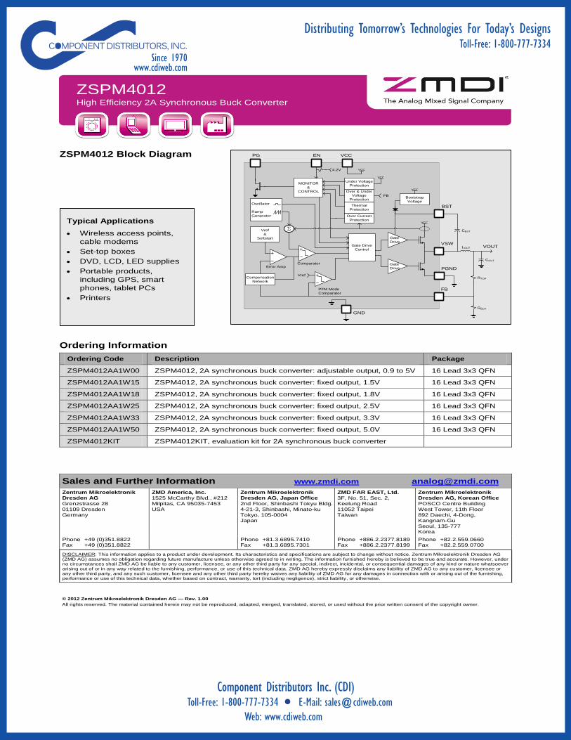
Typical Applications
Wireless access points,
cable modems
Set-top boxes
DVD, LCD, LED supplies
Portable products,
including GPS, smart
phones, tablet PCs
Printers
VCC
Over Current
Protection
Gate
Drive
Gate
Drive
Bootstrap
Voltage
VCC
Gate Drive
Control
FB
VSW
Vref
&
Softstart
Oscillator
Ramp
Generator
ComparatorError Amp
GND
Under Voltage
ProtectionMONITOR
&
CONTROL
Thermal
Protection
Over & Under
Voltage
Protection
VCC
FB
VCC
VCC
BST
VOUT
EN
PGND
PG
CBST
COUT
LOUT
RTOP
RBOT
PFM Mode
Comparator
Vref
4.2V
Compensation
Network
ZSPM4012 Block Diagram
Ordering Information
Ordering Code Description Package
ZSPM4012AA1W00 ZSPM4012, 2A synchronous buck converter: adjustable output, 0.9 to 5V 16 Lead 3x3 QFN
ZSPM4012AA1W15 ZSPM4012, 2A synchronous buck converter: fixed output, 1.5V 16 Lead 3x3 QFN
ZSPM4012AA1W18 ZSPM4012, 2A synchronous buck converter: fixed output, 1.8V 16 Lead 3x3 QFN
ZSPM4012AA1W25 ZSPM4012, 2A synchronous buck converter: fixed output, 2.5V 16 Lead 3x3 QFN
ZSPM4012AA1W33 ZSPM4012, 2A synchronous buck converter: fixed output, 3.3V 16 Lead 3x3 QFN
ZSPM4012AA1W50 ZSPM4012, 2A synchronous buck converter: fixed output, 5.0V 16 Lead 3x3 QFN
ZSPM4012KIT ZSPM4012KIT, evaluation kit for 2A synchronous buck converter
Sales and Further Information www.zmdi.com [email protected]
Zentrum Mikroelektronik Dresden AG
Grenzstrasse 28
01109 Dresden Germany
ZMD America, Inc.
1525 McCarthy Blvd., #212 Milpitas, CA 95035-7453
USA
Zentrum Mikroelektronik Dresden AG, Japan Office
2nd Floor, Shinbashi Tokyu Bldg.
4-21-3, Shinbashi, Minato-ku Tokyo, 105-0004 Japan
ZMD FAR EAST, Ltd.
3F, No. 51, Sec. 2, Keelung Road
11052 Taipei Taiwan
Zentrum Mikroelektronik Dresden AG, Korean Office
POSCO Centre Building
West Tower, 11th Floor 892 Daechi, 4-Dong, Kangnam-Gu Seoul, 135-777 Korea
Phone +49 (0)351.8822 Fax +49 (0)351.8822
Phone +81.3.6895.7410 Fax +81.3.6895.7301
Phone +886.2.2377.8189 Fax +886.2.2377.8199
Phone +82.2.559.0660 Fax +82.2.559.0700
DISCLAIMER: This information applies to a product under development. Its characteristics and specifications are subject to change without notice. Zentrum Mikroelektronik Dresden AG (ZMD AG) assumes no obligation regarding future manufacture unless otherwise agreed to in writing. The information furnished hereby is believed to be true and accurate. However, under no circumstances shall ZMD AG be liable to any customer, licensee, or any other third party for any special, indirect, incidental, or consequential damages of any kind or nature whatsoever arising out of or in any way related to the furnishing, performance, or use of this technical data. ZMD AG hereby expressly disclaims any liability of ZMD AG to any customer, licensee or any other third party, and any such customer, licensee and any other third party hereby waives any liability of ZMD AG for any damages in connection with or arising out of the furnishing, performance or use of this technical data, whether based on contract, warranty, tort (including negligence), strict liability, or otherwise.
Component Distributors Inc. (CDI) Toll-Free: 1-800-777-7334 E-Mail: [email protected]
Web: www.cdiweb.com/PortalMain.aspx?pid=704
Distributing Tomorrow’s Technologies For Today’s DesignsToll-Free: 1-800-777-7334
Since 1970http://www.cdiweb.com/PortalMain.aspx?pid=704
ZSPM4012 High Efficiency 2A Synchronous Buck Converter
Data Sheet
January 23, 2012
© 2012 Zentrum Mikroelektronik Dresden AG — Rev. 1.00
All rights reserved. The material contained herein may not be reproduced, adapted, merged, translated, stored, or used without the prior written consent of the copyright owner. The information furnished in this publication is subject to changes without notice.
4 of 19
Contents
1 ZSPM4012 Characteristics .................................................................................................................................. 6 1.1. Absolute Maximum Ratings .......................................................................................................................... 6 1.2. Thermal Characteristics ................................................................................................................................ 6 1.3. Recommended Operating Conditions .......................................................................................................... 6 1.4. Electrical Characteristics .............................................................................................................................. 7 1.5. Regulator Characteristics ............................................................................................................................. 8
2 Typical Performance Characteristics ................................................................................................................... 9 3 Description of Circuit ......................................................................................................................................... 12
3.1. Internal Protection Details........................................................................................................................... 13 3.1.1. Internal Current Limit ............................................................................................................................ 13 3.1.2. Thermal Shutdown ............................................................................................................................... 13 3.1.3. Reference Soft-Start ............................................................................................................................ 13 3.1.4. Output Over-Voltage ............................................................................................................................ 13 3.1.5. VCC Under-Voltage Lockout ................................................................................................................ 13
4 Application Circuits ............................................................................................................................................ 14 4.1. Selection of External Components ............................................................................................................. 14 4.2. Typical Application Circuits ......................................................................................................................... 14
5 Pin Configuration and Package ......................................................................................................................... 15 5.1. Marking Diagram & Pin-out......................................................................................................................... 16 5.2. Pin Description for 16 LEAD 3x3 QFN ....................................................................................................... 17 5.3. Detailed Pin Description ............................................................................................................................. 17
5.3.1. Unregulated Input, VCC (Pins # 2,3) ................................................................................................... 17 5.3.2. Bootstrap Control, BST (Pin #10) ........................................................................................................ 17 5.3.3. Sense Feedback, FB (Pin #5) .............................................................................................................. 17 5.3.4. Switching Output, VSW (Pins #12,13) ................................................................................................. 18 5.3.5. Ground, GND (Pin #4) .......................................................................................................................... 18 5.3.6. Power Ground, PGND (Pins #14,15) ................................................................................................... 18 5.3.7. Enable, High-Voltage, EN (Pin #9) ...................................................................................................... 18 5.3.8. PG Output, PG (Pin #8) ....................................................................................................................... 18
6 Ordering Information .......................................................................................................................................... 18 7 Related Documents ........................................................................................................................................... 19 8 Glossary ............................................................................................................................................................ 19 9 Document Revision History ............................................................................................................................... 19

Component Distributors Inc. (CDI) Toll-Free: 1-800-777-7334 E-Mail: [email protected]
Web: www.cdiweb.com/PortalMain.aspx?pid=704
Distributing Tomorrow’s Technologies For Today’s DesignsToll-Free: 1-800-777-7334
Since 1970http://www.cdiweb.com/PortalMain.aspx?pid=704
ZSPM4012 High Efficiency 2A Synchronous Buck Converter
Data Sheet
January 23, 2012
© 2012 Zentrum Mikroelektronik Dresden AG — Rev. 1.00
All rights reserved. The material contained herein may not be reproduced, adapted, merged, translated, stored, or used without the prior written consent of the copyright owner. The information furnished in this publication is subject to changes without notice.
5 of 19
List of Figures
Figure 2.1: Startup Response ..................................................................................................................................... 9 Figure 2.2: 100mA to 1A Load Step (Vcc= 12V, Vout =1,8V) .................................................................................... 9 Figure 2.3: 100mA to 2A Load (Vcc=12V, Vout = 1,8V) ............................................................................................. 9 Figure 2.4: 100mA t0 1A Load Step (Vcc=12V, Vout = 3,3V) .................................................................................... 9 Figure 2.5: 100mA to 2A Load Step (Vcc=12V, Vout = 3.3V) .................................................................................... 9 Figure 2.6: Line Transient Response (VCC=10V to 15V, Vout = 3.3V) ..................................................................... 9 Figure 2.7: Load Regulation ..................................................................................................................................... 10 Figure 2.8: Line Regulation (IOUT=1A) .................................................................................................................... 10 Figure 2.9: Efficiency vs. Output Current ( VOUT = 1.8V) ........................................................................................... 10 Figure 2.10: Efficiency vs. Output Current ( VOUT = 3.3V) ......................................................................................... 10 Figure 2.11: Efficiency vs. Output Current ( VOUT = 5V) ............................................................................................ 10 Figure 2.12: Efficiency vs. Input Voltage (VOUT = 3.3V) ............................................................................................ 10 Figure 2.13: Standby Current vs. Input Voltage ....................................................................................................... 11 Figure 2.14: Standby Current vs. Temperature ........................................................................................................ 11 Figure 2.15: Output Voltage vs. Temperature .......................................................................................................... 11 Figure 2.16: Oscillator Frequency vs. Temperature (Iout=300mA) .......................................................................... 11 Figure 2.17: Quiescent Current vs. Temperature (No load) ..................................................................................... 11 Figure 2.18: Input Current vs. Temperature (No load, No switching) ...................................................................... 11 Figure 3.1: ZSPM4012 Block Diagram................................................................................................................... 12 Figure 3.2: Monitor and Control Logic Functionality .............................................................................................. 13 Figure 4.1: Typical Application for Adjustable Output Voltage ............................................................................... 14 Figure 4.2: Typical Application for Fixed Output Voltage ....................................................................................... 14 Figure 5.1: ZSPM4012 Package Drawing .............................................................................................................. 15 Figure 5.2: 16 Lead 3x3 QFN (top view) .................................................................................................................. 16
List of Tables
Table 1.1: Absolute Maximum Ratings ....................................................................................................................... 6 Table 1.2: Thermal Characteristics ............................................................................................................................. 6 Table 1.3: Recommended Operating Conditions ....................................................................................................... 6 Table 1.4: Electrical Characteristics ........................................................................................................................... 7 Table 1.5: Regulator Characteristics .......................................................................................................................... 8 Table 5.1: Pin Description, 16 Lead, 3x3 QFN ......................................................................................................... 17

Component Distributors Inc. (CDI) Toll-Free: 1-800-777-7334 E-Mail: [email protected]
Web: www.cdiweb.com/PortalMain.aspx?pid=704
Distributing Tomorrow’s Technologies For Today’s DesignsToll-Free: 1-800-777-7334
Since 1970http://www.cdiweb.com/PortalMain.aspx?pid=704
ZSPM4012 High Efficiency 2A Synchronous Buck Converter
Data Sheet
January 23, 2012
© 2012 Zentrum Mikroelektronik Dresden AG — Rev. 1.00
All rights reserved. The material contained herein may not be reproduced, adapted, merged, translated, stored, or used without the prior written consent of the copyright owner. The information furnished in this publication is subject to changes without notice.
6 of 19
1 ZSPM4012 Characteristics
1.1. Absolute Maximum Ratings
Over operating free–air temperature range unless otherwise noted(1,2)
Table 1.1: Absolute Maximum Ratings
Parameter Value UNIT
VCC
-0.3 to 26.4 V
BST -0.3 to (VCC+6) V
VSW -1 to 26.4 V
EN, PG, FB -0.3 to 6 V
Continuous total power dissipation See Dissipation Rating Table
Electrostatic Discharge – Human Body Model +/-2k V
Electrostatic Discharge – Charge Device Model +/-500 V
Lead Temperature (soldering, 10 seconds) 260 C
(1) Stresses beyond those listed under “absolute maximum ratings” may cause permanent damage to the device. These are stress ratings
only and functional operation of the device at these or any other conditions beyond those indicated under “recommended operat ing
conditions” is not implied. Exposure to absolute–maximum–rated conditions for extended periods may affect device reliability.
(2) All voltage values are with respect to network ground terminal
1.2. Thermal Characteristics
Table 1.2: Thermal Characteristics
Symbol Parameter Value Unit
JA Thermal Resistance Junction to Air (Note 1) 38 °C/W
TSTG Storage Temperature Range -65 to 150 °C
TJ MAX Maximum Junction Temperature 150 °C
TJ Operating Junction Temperature Range -40 to 125 °C
Note 1: Assumes SOIC-8EP 1 in2 area of 2 oz copper and 25C ambient temperature.
1.3. Recommended Operating Conditions
Table 1.3: Recommended Operating Conditions
Symbol Parameter Min Typ Max Unit
VCC
Input Operating Voltage 6 12 24 V
CBST Bootstrap Capacitor 17.6 22 26.4 nF
LOUT Output Filter Inductor Typical Value (Note 1) 3.76 4.7 5.64 uH
COUT Output Filter Capacitor Typical Value (Note 2) 33 44 (2 x 22) uF
COUT-ESR Output Filter Capacitor ESR 2 100 m
CBYPASS Input Supply Bypass Capacitor Typical Value (Note 3) 8 10 uF
Note 1: For best performance, an inductor with a saturation current rating higher than the maximum VOUT load requirement plus the inductor current ripple.
Note 2: For best performance, a low ESR ceramic capacitor should be used. Note 3: For best performance, a low ESR ceramic capacitor should be used. If CBYPASS is not a low ESR ceramic capacitor, a 0.1uF ceramic
capacitor should be added in parallel to CBYPASS.

Component Distributors Inc. (CDI) Toll-Free: 1-800-777-7334 E-Mail: [email protected]
Web: www.cdiweb.com/PortalMain.aspx?pid=704
Distributing Tomorrow’s Technologies For Today’s DesignsToll-Free: 1-800-777-7334
Since 1970http://www.cdiweb.com/PortalMain.aspx?pid=704
ZSPM4012 High Efficiency 2A Synchronous Buck Converter
Data Sheet
January 23, 2012
© 2012 Zentrum Mikroelektronik Dresden AG — Rev. 1.00
All rights reserved. The material contained herein may not be reproduced, adapted, merged, translated, stored, or used without the prior written consent of the copyright owner. The information furnished in this publication is subject to changes without notice.
7 of 19
1.4. Electrical Characteristics
Electrical Characteristics, TJ = -40°C to 125°C, VCC = 12V (unless otherwise noted)
Table 1.4: Electrical Characteristics
Symbol Parameter Condition Min Typ Max Unit
VCC Supply Voltage
VCC Input Supply Voltage 6 24 V
ICC-NORM Quiescent current Normal Mode
VCC = 12V, ILOAD = 0A 5.2 mA
ICC-NOSWITCH Quiescent current Normal Mode – Non-switching
VCC=12V, ILOAD=0A, Non-switching
2.3 mA
ICC-STBY Quiescent current Standby Mode
VCC = 12V, EN = 0V 5 10 uA
VCC Under Voltage Lockout
VCC-UV Input Supply Under Voltage Threshold
VCC Increasing 5.5 6.0 V
VCC-
UV_HYST Input Supply Under Voltage Threshold Hysteresis
650 mV
OSC
FOSC Oscillator Frequency 0.9 1 1.1 MHz
PG Open Drain Output
TPG PG Release Timer 10 Ms IOH-PG High-Level Output Leakage VPG = 5V 0.5 uA
VOL-PG Low-Level Output Voltage IPG = -0.3mA 0.01 V
EN Input Voltage Thresholds
VIH-EN High Level Input Voltage 2.2 V
VIL-EN Low Level Input Voltage 0.8 V
VHYST-EN Input Hysteresis 480 mV
IIN-EN Input Leakage VEN=5V 3.5 uA
VEN=0V -1.5 uA
Thermal Shutdown
TSD Thermal Shutdown Junction Temperature
Note: not tested in production
150 170 °C
TSDHYST TSD Hysteresis 10 °C
Component Distributors Inc. (CDI) Toll-Free: 1-800-777-7334 E-Mail: [email protected]
Web: www.cdiweb.com/PortalMain.aspx?pid=704
Distributing Tomorrow’s Technologies For Today’s DesignsToll-Free: 1-800-777-7334
Since 1970http://www.cdiweb.com/PortalMain.aspx?pid=704
ZSPM4012 High Efficiency 2A Synchronous Buck Converter
Data Sheet
January 23, 2012
© 2012 Zentrum Mikroelektronik Dresden AG — Rev. 1.00
All rights reserved. The material contained herein may not be reproduced, adapted, merged, translated, stored, or used without the prior written consent of the copyright owner. The information furnished in this publication is subject to changes without notice.
8 of 19
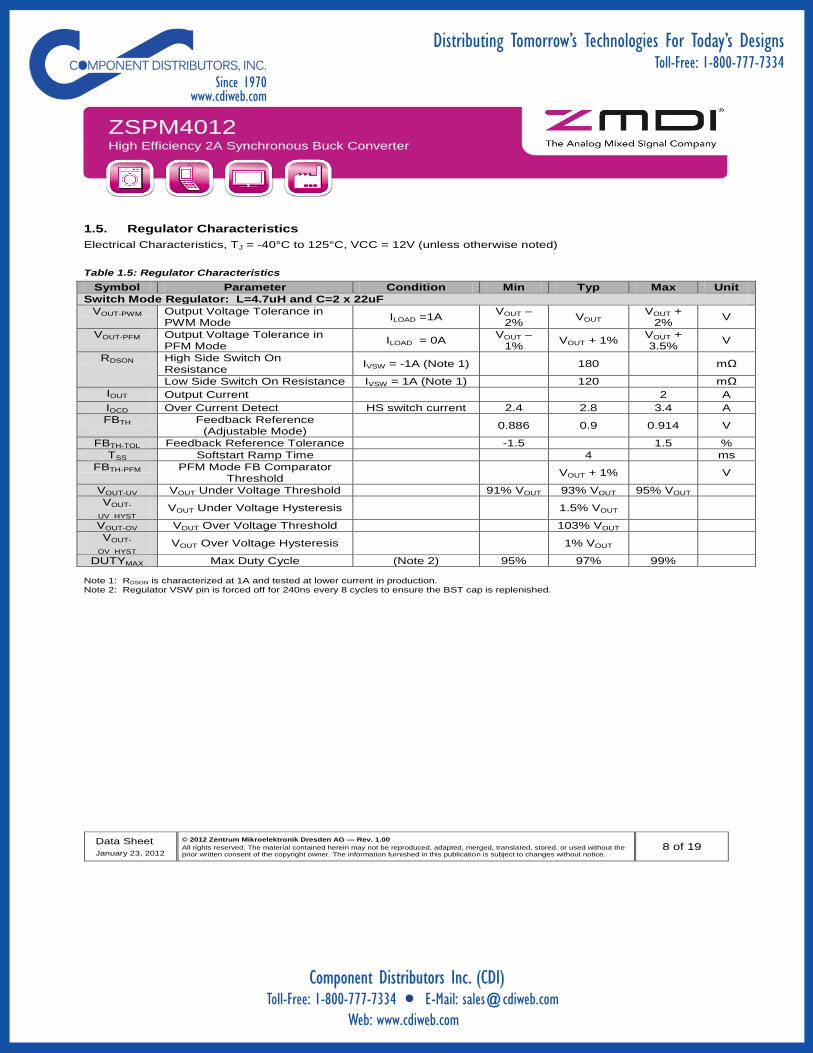
1.5. Regulator Characteristics
Electrical Characteristics, TJ = -40°C to 125°C, VCC = 12V (unless otherwise noted)
Table 1.5: Regulator Characteristics
Symbol Parameter Condition Min Typ Max Unit
Switch Mode Regulator: L=4.7uH and C=2 x 22uF
VOUT-PWM Output Voltage Tolerance in PWM Mode
ILOAD =1A VOUT –
2% VOUT
VOUT + 2%
V
VOUT-PFM Output Voltage Tolerance in PFM Mode
ILOAD = 0A VOUT –
1% VOUT + 1%
VOUT + 3.5%
V
RDSON High Side Switch On Resistance
IVSW = -1A (Note 1) 180 mΩ
Low Side Switch On Resistance IVSW = 1A (Note 1) 120 mΩ
IOUT Output Current 2 A
IOCD Over Current Detect HS switch current 2.4 2.8 3.4 A
FBTH Feedback Reference (Adjustable Mode)
0.886 0.9 0.914 V
FBTH-TOL Feedback Reference Tolerance -1.5 1.5 %
TSS Softstart Ramp Time 4 ms
FBTH-PFM PFM Mode FB Comparator Threshold
VOUT + 1% V
VOUT-UV VOUT Under Voltage Threshold 91% VOUT 93% VOUT 95% VOUT
VOUT-
UV_HYST VOUT Under Voltage Hysteresis 1.5% VOUT
VOUT-OV VOUT Over Voltage Threshold 103% VOUT
VOUT-
OV_HYST VOUT Over Voltage Hysteresis 1% VOUT
DUTYMAX Max Duty Cycle (Note 2) 95% 97% 99% Note 1: RDSON is characterized at 1A and tested at lower current in production. Note 2: Regulator VSW pin is forced off for 240ns every 8 cycles to ensure the BST cap is replenished.

Component Distributors Inc. (CDI) Toll-Free: 1-800-777-7334 E-Mail: [email protected]
Web: www.cdiweb.com/PortalMain.aspx?pid=704
Distributing Tomorrow’s Technologies For Today’s DesignsToll-Free: 1-800-777-7334
Since 1970http://www.cdiweb.com/PortalMain.aspx?pid=704
ZSPM4012 High Efficiency 2A Synchronous Buck Converter
Data Sheet
January 23, 2012
© 2012 Zentrum Mikroelektronik Dresden AG — Rev. 1.00
All rights reserved. The material contained herein may not be reproduced, adapted, merged, translated, stored, or used without the prior written consent of the copyright owner. The information furnished in this publication is subject to changes without notice.
9 of 19
2 Typical Performance Characteristics
TJ = -40°C to 125°C, VCC = 12V (unless otherwise noted)
Figure 2.1: Startup Response
Figure 2.2: 100mA to 1A Load Step (Vcc= 12V, Vout =1,8V)
Figure 2.3: 100mA to 2A Load (Vcc=12V, Vout = 1,8V)
Figure 2.4: 100mA t0 1A Load Step (Vcc=12V, Vout = 3,3V)
Figure 2.5: 100mA to 2A Load Step (Vcc=12V, Vout =
3.3V)
Figure 2.6: Line Transient Response (VCC=10V to 15V,
Vout = 3.3V)

Component Distributors Inc. (CDI) Toll-Free: 1-800-777-7334 E-Mail: [email protected]
Web: www.cdiweb.com/PortalMain.aspx?pid=704
Distributing Tomorrow’s Technologies For Today’s DesignsToll-Free: 1-800-777-7334
Since 1970http://www.cdiweb.com/PortalMain.aspx?pid=704
ZSPM4012 High Efficiency 2A Synchronous Buck Converter
Data Sheet
January 23, 2012
© 2012 Zentrum Mikroelektronik Dresden AG — Rev. 1.00
All rights reserved. The material contained herein may not be reproduced, adapted, merged, translated, stored, or used without the prior written consent of the copyright owner. The information furnished in this publication is subject to changes without notice.
10 of 19
Figure 2.7: Load Regulation
Figure 2.8: Line Regulation (IOUT=1A)
Figure 2.9: Efficiency vs. Output Current ( VOUT = 1.8V)
Figure 2.10: Efficiency vs. Output Current ( VOUT = 3.3V)
Figure 2.11: Efficiency vs. Output Current ( VOUT = 5V)
Figure 2.12: Efficiency vs. Input Voltage (VOUT = 3.3V)

Component Distributors Inc. (CDI) Toll-Free: 1-800-777-7334 E-Mail: [email protected]
Web: www.cdiweb.com/PortalMain.aspx?pid=704
Distributing Tomorrow’s Technologies For Today’s DesignsToll-Free: 1-800-777-7334
Since 1970http://www.cdiweb.com/PortalMain.aspx?pid=704
ZSPM4012 High Efficiency 2A Synchronous Buck Converter
Data Sheet
January 23, 2012
© 2012 Zentrum Mikroelektronik Dresden AG — Rev. 1.00
All rights reserved. The material contained herein may not be reproduced, adapted, merged, translated, stored, or used without the prior written consent of the copyright owner. The information furnished in this publication is subject to changes without notice.
11 of 19
Figure 2.13: Standby Current vs. Input Voltage
Figure 2.14: Standby Current vs. Temperature
Figure 2.15: Output Voltage vs. Temperature
Figure 2.16: Oscillator Frequency vs. Temperature
(Iout=300mA)
Figure 2.17: Quiescent Current vs. Temperature (No load)
Figure 2.18: Input Current vs. Temperature
(No load, No switching)

Component Distributors Inc. (CDI) Toll-Free: 1-800-777-7334 E-Mail: [email protected]
Web: www.cdiweb.com/PortalMain.aspx?pid=704
Distributing Tomorrow’s Technologies For Today’s DesignsToll-Free: 1-800-777-7334
Since 1970http://www.cdiweb.com/PortalMain.aspx?pid=704
ZSPM4012 High Efficiency 2A Synchronous Buck Converter
Data Sheet
January 23, 2012
© 2012 Zentrum Mikroelektronik Dresden AG — Rev. 1.00
All rights reserved. The material contained herein may not be reproduced, adapted, merged, translated, stored, or used without the prior written consent of the copyright owner. The information furnished in this publication is subject to changes without notice.
12 of 19
3 Description of Circuit
The ZSPM4012 current-mode synchronous step-down power supply product can be used in the commercial, industrial, and automotive market segments. It includes flexibility for a wide range of output voltages and is optimized for high efficiency power conversion with low RDSON integrated synchronous switches. A 1MHz internal switching frequency facilitates low cost LC filter combinations. Additionally, the fixed-output versions enable a minimum external component count to provide a complete regulation solution with only 4 external components: an input bypass capacitor, an inductor, an output capacitor, and the bootstrap capacitor. The regulator automatically transitions between PFM and PWM mode to maximize efficiency for the load demand.
Figure 3.1: ZSPM4012 Block Diagram
VCC
Over Current
Protection
Gate
Drive
Gate
Drive
Bootstrap
Voltage
VCC
Gate Drive
Control
FB
VSW
Vref
&
Softstart
Oscillator
Ramp
Generator
ComparatorError Amp
GND
Under Voltage
ProtectionMONITOR
&
CONTROL
Thermal
Protection
Over & Under
Voltage
Protection
VCC
FB
VCC
VCC
BST
VOUT
EN
PGND
PG
CBST
COUT
LOUT
RTOP
RBOT
PFM Mode
Comparator
Vref
4.2V
Compensation
Network

Component Distributors Inc. (CDI) Toll-Free: 1-800-777-7334 E-Mail: [email protected]
Web: www.cdiweb.com/PortalMain.aspx?pid=704
Distributing Tomorrow’s Technologies For Today’s DesignsToll-Free: 1-800-777-7334
Since 1970http://www.cdiweb.com/PortalMain.aspx?pid=704
ZSPM4012 High Efficiency 2A Synchronous Buck Converter
Data Sheet
January 23, 2012
© 2012 Zentrum Mikroelektronik Dresden AG — Rev. 1.00
All rights reserved. The material contained herein may not be reproduced, adapted, merged, translated, stored, or used without the prior written consent of the copyright owner. The information furnished in this publication is subject to changes without notice.
13 of 19
Figure 3.2: Monitor and Control Logic Functionality
TSD Filter
VCC-UV Filter
Internal
PORFilter
FilterEN
VOUT-UV Filter
PG
ENABLE
REGULATOR
VOUT-OV Filter
IOCD OCD_Filter
TRISTATE
VSW OUTPUT
3.1. Internal Protection Details
3.1.1. Internal Current Limit
The current through the high side FET is sensed on a cycle-by-cycle basis and if current limit is reached, it will abbreviate the cycle. In addition, the device senses the FB pin to identify hard short conditions and will direct the VSW output to skip 4 cycles if current limit occurs when FB is low. This allows current built up in the inductor during the minimum on time to decay sufficiently.
Current limit is always active when the regulator is enabled. Soft start ensures that current limit does not prevent regulator startup.
An additional feature of the over-current protection circuitry is that, under extended over current conditions, the device will automatically disable. A simple toggle of the Enable pin will return the device to normal operation.
3.1.2. Thermal Shutdown
If the temperature of the die exceeds 170°C (typical), the VSW outputs will tri-state to protect the device from damage. The PG and all other protection circuitry will stay active to inform the system of the failure mode. Once the device cools to 160°C (typical), the device will attempt to start up again, following the normal soft start sequence. If the device reaches 170°C, the shutdown/restart sequence will repeat.
3.1.3. Reference Soft-Start
The reference in this device is ramped at a rate of 4ms to prevent the output from overshoot during startup. This ramp restarts whenever there is a rising edge sensed on the Enable pin. This occurs in both the fixed and adjustable versions. During the soft start ramp, current limit is still active, and will still protect the device in case of a short on the output.
3.1.4. Output Over-Voltage
If the output of the regulator exceeds 103% of the regulation voltage, the VSW outputs will tri-state to protect the device from damage. This check occurs at the start of each switching cycle. If it occurs during the middle of a cycle, the switching for that cycle will complete, and the VSW outputs will tri-state at the beginning of the next cycle.
3.1.5. VCC Under-Voltage Lockout
The device is held in the off state until VCC reaches 5.75V (typical). There is a 500mV hysteresis on this input, which requires the input to fall below 5.25V (typical) before the device will disable.
Component Distributors Inc. (CDI) Toll-Free: 1-800-777-7334 E-Mail: [email protected]
Web: www.cdiweb.com/PortalMain.aspx?pid=704
Distributing Tomorrow’s Technologies For Today’s DesignsToll-Free: 1-800-777-7334
Since 1970http://www.cdiweb.com/PortalMain.aspx?pid=704
ZSPM4012 High Efficiency 2A Synchronous Buck Converter
Data Sheet
January 23, 2012
© 2012 Zentrum Mikroelektronik Dresden AG — Rev. 1.00
All rights reserved. The material contained herein may not be reproduced, adapted, merged, translated, stored, or used without the prior written consent of the copyright owner. The information furnished in this publication is subject to changes without notice.
14 of 19
4 Application Circuits
4.1. Selection of External Components
The internal compensation is optimized for a 44uF output capacitor and a 4.7uH inductor. The minimum allowable value for the output capacitor is 33uF. To keep the output ripple low, a low ESR (less than 35mOhm) ceramic is recommended. The inductor range is 4.7uH +/-20%. For optimal over-current protection, the inductor should be able to handle up to the regulator current limit without saturation.
4.2. Typical Application Circuits
Figure 4.1: Typical Application for Adjustable Output Voltage
ZS
PM
4012
VOUTP
GN
DVSW
VCC
FB
GN
DBST
VCC
PG PG
RTOP
RBOT
10 kohm
(optional)
VCC or VOUT
ENEN
Figure 4.2: Typical Application for Fixed Output Voltage
ZS
PM
4012
VOUT
EN
PG
ND
VSW
VCC
FB
GN
D
VCC
EN
PG PG
10 kohm
(optional)
VCC or VOUT
BST

Component Distributors Inc. (CDI) Toll-Free: 1-800-777-7334 E-Mail: [email protected]
Web: www.cdiweb.com/PortalMain.aspx?pid=704
Distributing Tomorrow’s Technologies For Today’s DesignsToll-Free: 1-800-777-7334
Since 1970http://www.cdiweb.com/PortalMain.aspx?pid=704
ZSPM4012 High Efficiency 2A Synchronous Buck Converter
Data Sheet
January 23, 2012
© 2012 Zentrum Mikroelektronik Dresden AG — Rev. 1.00
All rights reserved. The material contained herein may not be reproduced, adapted, merged, translated, stored, or used without the prior written consent of the copyright owner. The information furnished in this publication is subject to changes without notice.
15 of 19
5 Pin Configuration and Package
Figure 5.1: ZSPM4012 Package Drawing
Component Distributors Inc. (CDI) Toll-Free: 1-800-777-7334 E-Mail: [email protected]
Web: www.cdiweb.com/PortalMain.aspx?pid=704
Distributing Tomorrow’s Technologies For Today’s DesignsToll-Free: 1-800-777-7334
Since 1970http://www.cdiweb.com/PortalMain.aspx?pid=704
ZSPM4012 High Efficiency 2A Synchronous Buck Converter
Data Sheet
January 23, 2012
© 2012 Zentrum Mikroelektronik Dresden AG — Rev. 1.00
All rights reserved. The material contained herein may not be reproduced, adapted, merged, translated, stored, or used without the prior written consent of the copyright owner. The information furnished in this publication is subject to changes without notice.
16 of 19
5.1. Marking Diagram & Pin-out
Figure 5.2: 16 Lead 3x3 QFN (top view)
4012: Part Name A: Revision XXXXX: Lot number (last five digits) O: Pin 1 mark VL: Voltage level
15 = 1.5V
18 = 1.8V
25 = 2.5V
33 = 3.3V
50 = 5.0V
00 = 0.9V – 5.0V variable
MY: Date Code M = Month
1 = January
2 = February
3 = March
4 = April
5 = May
6 = June
7 = July
8 = August
9 = September
A = October
B = November
C = December Y = Year
A = 2011
B = 2012
C = 201
Etc.

Component Distributors Inc. (CDI) Toll-Free: 1-800-777-7334 E-Mail: [email protected]
Web: www.cdiweb.com/PortalMain.aspx?pid=704
Distributing Tomorrow’s Technologies For Today’s DesignsToll-Free: 1-800-777-7334
Since 1970http://www.cdiweb.com/PortalMain.aspx?pid=704
ZSPM4012 High Efficiency 2A Synchronous Buck Converter
Data Sheet
January 23, 2012
© 2012 Zentrum Mikroelektronik Dresden AG — Rev. 1.00
All rights reserved. The material contained herein may not be reproduced, adapted, merged, translated, stored, or used without the prior written consent of the copyright owner. The information furnished in this publication is subject to changes without notice.
17 of 19
5.2. Pin Description for 16 LEAD 3x3 QFN
Table 5.1: Pin Description, 16 Lead, 3x3 QFN
Name Pin # Function Description
VSW 1 Switching Voltage Node Connected to 4.7uH (typical) inductor
VCC 2 Input Voltage Input voltage
VCC 3 Input Voltage Input voltage
GND 4 GND Primary ground for the majority of the device except the
low-side power FET.
FB 5 Feedback Input Regulator FB Voltage. Connects to VOUT for fixed-mode
and the output resistor divider for adjustable mode.
NC 6 No Connect Not Connected
NC 7 No Connect Not Connected
PG 8 PG Output Open-drain output.
EN 9 Enable Input Above 2.2V the device is enabled. GND the pin to
disable the device. Includes internal pull-up.
BST 10 Bootstrap Capacitor Bootstrap capacitor for the high-side FET gate driver.
22nF ceramic capacitor from BST pin to VSW pin
VCC 11 Input Voltage Input Voltage
VSW 12 Switching Voltage Node Connected to 4.7uH (typical) inductor
VSW 13 Switching Voltage Node Connected to 4.7uH (typical) inductor
PGND 14 Power GND GND supply for internal low-side FET/integrated diode
PGND 15 Power GND GND supply for internal low-side FET/integrated diode
VSW 16 Switching Voltage Node Connected to 4.7uH (typical) inductor
5.3. Detailed Pin Description
5.3.1. Unregulated Input, VCC (Pins # 2,3)
This terminal is the unregulated input voltage source for the IC. It is recommended that a 10uF bypass capacitor be placed close to the device for best performance. Since this is the main supply for the IC, good layout practices need to be followed for this connection.
5.3.2. Bootstrap Control, BST (Pin #10)
This terminal will provide the bootstrap voltage required for the upper internal NMOS switch of the buck regulator. An external ceramic capacitor placed between the BST input terminal and the VSW pin will provide the necessary voltage for the upper switch. In normal operation the capacitor is re-charged on every low side synchronous switching action. In the case of where the switch mode approaches 100% duty cycle for the high side FET, the device will automatically reduce the duty cycle switch to a minimum off time on every 8
th cycle to allow this
capacitor to re-charge.
5.3.3. Sense Feedback, FB (Pin #5)
This is the input terminal for the output voltage feedback. For the fixed-mode versions, this should be connected directly to VOUT. The connection on the PCB should be kept as short as possible, and should be made as close as possible to the capacitor. The trace should not be shared with any other connection.
Component Distributors Inc. (CDI) Toll-Free: 1-800-777-7334 E-Mail: [email protected]
Web: www.cdiweb.com/PortalMain.aspx?pid=704
Distributing Tomorrow’s Technologies For Today’s DesignsToll-Free: 1-800-777-7334
Since 1970http://www.cdiweb.com/PortalMain.aspx?pid=704
ZSPM4012 High Efficiency 2A Synchronous Buck Converter
Data Sheet
January 23, 2012
© 2012 Zentrum Mikroelektronik Dresden AG — Rev. 1.00
All rights reserved. The material contained herein may not be reproduced, adapted, merged, translated, stored, or used without the prior written consent of the copyright owner. The information furnished in this publication is subject to changes without notice.
18 of 19
For adjustable-mode versions, this should be connected to the external resistor divider. To choose the resistors, use the following equation: VOUT = 0.9 (1 + RTOP/RBOT) The input to the FB pin is high impedance, and input current should be less than 100nA. As a result, good layout practices are required for the feedback resistors and feedback traces. When using the adjustable version, the feedback trace should be kept as short and narrow as possible to reduce stray capacitance and the injection of noise.
5.3.4. Switching Output, VSW (Pins #12,13)
This is the switching node of the regulator. It should be connected directly to the 4.7uH inductor with a wide, short trace and to one end of the Bootstrap capacitor. It is switching between VCC and PGND at the switching frequency.
5.3.5. Ground, GND (Pin #4)
This ground is used for the majority of the device including the analog reference, control loop, and other circuits.
5.3.6. Power Ground, PGND (Pins #14,15)
This is a separate ground connection used for the low-side synchronous switch to isolate switching noise from the rest of the device.
5.3.7. Enable, High-Voltage, EN (Pin #9)
This is the input terminal to activate the regulator. The input threshold is TTL/CMOS compatible. It also has an internal pull-up to ensure a stable state if the pin is disconnected.
5.3.8. PG Output, PG (Pin #8)
This is an open drain, active low output. The switched mode output voltage is monitored and the PG line will remain low until the output voltage reaches the VOUT-UV threshold. Once the internal comparator detects that the output voltage is above the desired threshold, an internal delay timer is activated and the PG line is de-asserted (to high) once this delay timer expires. In the event the output voltage decreases below VOUT-UV, the PG line will be asserted low and remain low until the output rises above VOUT-UV and the delay timer times out. See Figure 2 for the circuit schematic for the PG signal.
6 Ordering Information
Explanation of Ordering Codes: ZSPM2012AA1Wxx: “W” = 7” reel with 1000 ICs ZSPM2012AA1Rxx: “R” = 13” reel with 3300 ICs
Product Sales Code Description Package
ZSPM4012AA1W00 ZSPM4012, 2A synchronous buck converter: adjustable output, 0.9 to 5V 16 Lead 3x3 QFN
ZSPM4012AA1W15 ZSPM4012, 2A synchronous buck converter: fixed output, 1.5V 16 Lead 3x3 QFN
ZSPM2012AA1W18 ZSPM4012, 2A synchronous buck converter: fixed output, 1.8V 16 Lead 3x3 QFN
ZSPM4012AA1W25 ZSPM4012, 2A synchronous buck converter: fixed output, 2.5V 16 Lead 3x3 QFN
ZSPM4012AA1W33 ZSPM4012, 2A synchronous buck converter: fixed output, 3.3V 16 Lead 3x3 QFN
ZSPM4012AA1W50 ZSPM4012, 2A synchronous buck converter: fixed output, 5.0V 16 Lead 3x3 QFN
ZSPM4012KIT ZSPM4012KIT, evaluation kit for 2A synchronous buck converter
Component Distributors Inc. (CDI) Toll-Free: 1-800-777-7334 E-Mail: [email protected]
Web: www.cdiweb.com/PortalMain.aspx?pid=704
Distributing Tomorrow’s Technologies For Today’s DesignsToll-Free: 1-800-777-7334
Since 1970http://www.cdiweb.com/PortalMain.aspx?pid=704
ZSPM4012 High Efficiency 2A Synchronous Buck Converter
Data Sheet
January 23, 2012
© 2012 Zentrum Mikroelektronik Dresden AG — Rev. 1.00
All rights reserved. The material contained herein may not be reproduced, adapted, merged, translated, stored, or used without the prior written consent of the copyright owner. The information furnished in this publication is subject to changes without notice.
19 of 19
7 Related Documents
Document File Name
ZSPM4011 Datasheet High Efficiency 1A Synchronous Buck Converter
ZSPM4013 Datasheet High Efficiency 3A Synchronous Buck Converter
ZSPM1000, ZSPM9000 Datasheets Single-Phase, Single-Rail true digital PWM controller
Visit ZMDI’s website www.zmdi.com or contact your nearest sales office for the latest version of these documents.
8 Glossary
Term Description
Buck converter Step-down converter; converts a higher DC input voltage to a lower DC output voltage with high efficiency
Synchronous rectification
is a technique for improving the efficiency of rectification by replacing diodes with actively-controlled switches such as transistors
PWM Pulse Width Modulation (fixed frequency)
PFM Pulse Frequency Modulation (fixed pulse width)
ESR Equivalent Series Resistance
Bootstrap control
When using an N-Channel Power MOSFET transistor as a high-side switch for the converter switching output, a gate voltage higher than the supply voltage is necessary to turn the transistor fully on.
For this purpose, a charge pump circuit, called bootstrap control is implemented to provide this high supply voltage for the high-side power MOSFET driver block.
9 Document Revision History
Revision Date Description
1.00 23-Jan-2012 First release
Sales and Further Information www.zmdi.com [email protected]
Zentrum Mikroelektronik
Dresden AG
Grenzstrasse 28 01109 Dresden Germany
ZMD America, Inc.
1525 McCarthy Blvd., #212 Milpitas, CA 95035-7453 USA
Zentrum Mikroelektronik
Dresden AG, Japan Office
2nd Floor, Shinbashi Tokyu Bldg. 4-21-3, Shinbashi, Minato-ku Tokyo, 105-0004 Japan
ZMD FAR EAST, Ltd.
3F, No. 51, Sec. 2, Keelung Road 11052 Taipei Taiwan
Zentrum Mikroelektronik
Dresden AG, Korean Office
POSCO Centre Building West Tower, 11th Floor 892 Daechi, 4-Dong, Kangnam-Gu Seoul, 135-777 Korea
Phone +49 (0)351.8822 Fax +49 (0)351.8822
Phone +81.3.6895.7410 Fax +81.3.6895.7301
Phone +886.2.2377.8189 Fax +886.2.2377.8199
Phone +82.2.559.0660 Fax +82.2.559.0700
DISCLAIMER: This information applies to a product under development. Its characteristics and specifications are subject to change without notice. Zentrum Mikroelektronik Dresden AG (ZMD AG) assumes no obligation regarding future manufacture unless otherwise agreed to in writing. The information furnished hereby is believed to be true and accurate. However, under no circumstances shall ZMD AG be liable to any customer, licensee, or any other third party for any special, indirect, incidental, or consequential damages of any kind or nature whatsoever arising out of or in any way related to the furnishing, performance, or use of this technical data. ZMD AG hereby expressly disclaims any liability of ZMD AG to any customer, licensee or any other third party, and any such customer, licensee and any other third party hereby waives any liability of ZMD AG for any damages in connection with or arising out of the furnishing, performance or use of this technical data, whether based on contract, warranty, tort (including negligence), strict liability, or otherwise.