research review 2005 - eth zürich - homepage | eth zürich
TRANSCRIPT
Research Review 2005
Integrated Systems Laboratory
Microelectronics Design CenterEidgenössische Technische Hochschule Zürich
Swiss Federal Institute of Technology Zurich
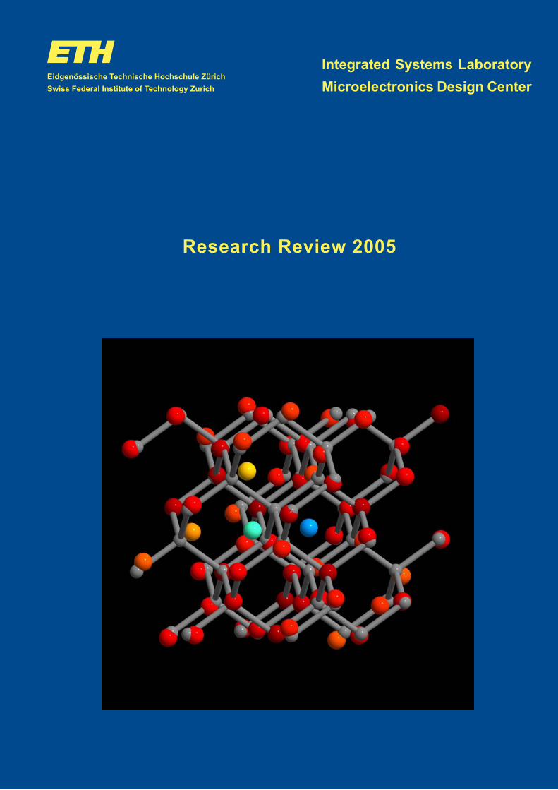
The picture on the cover is a freeze image of an ab initio molecular dynamics simulation of the self-inter-stitial defect in silicon. The silicon atoms are colored according to their distance to the closest lattice site of a reference lattice, shown in grey. The two atoms with the largest distance are part of the defect.
One of the consequences of the ongoing miniaturization in semiconductor technology is that standard process simu-standard process simu-lation tools based on continuum models cannot provide accurate and predictive results for such small geometries. Therefore, the understanding and physics-based simula-tion of the devices require a simulation paradigm change to the atomistic realm. Moreover, advanced and future technologies need to use new materials. These material systems have to be investigated by atomistic simulations
in order to improve insight view and performance of such technologies. The investigation of these new compounds by simulations on the atomistic level is a prerequisite for the optimization of the new technologies.
Ab initio simulations based on Density Functional Theory (DFT) allow for the examination of band structures, elec-trical and magnetic properties, as well as binding ener-gies and migration energy barriers of atomic processes. In addition, molecular dynamics DFT simulations are per-formed in order to evaluate diffusion mechanisms and dif-fusion constants for defects and dopants in a host mate-rial. Most of the atomistic parameters calculated this way are inaccessible to direct experimental measurements and therefore provide invaluable information for the un-derstanding and development of new technologies. The projects involved in atomistic simulations are focusing on the study of point defect diffusion and electrical do-nor deactivation in silicon. Also, the behavior of light alkali and alkaline earth metals in conjunction with n-type silicon doping is investigated. Further information can be found on pages 58 (right) and 59.
Post processing of first principles calculations: Evalua-tion of different silicon interstitial configurations by means of a Voronoi cell analysis in the diamond lattice.
Cover Image: Atomistic Simulations in Nanoelectronic Technologies
Address of the Laboratory:
ETH Zürich Integrated Systems Laboratory ETZ J81 and J96 Gloriastr. 35 8092 Zurich, Switzerland
Phone: +41 44 632 42 68 Fax: +41 44 632 11 94 e-mail: [email protected] www: http://www.iis.ee.ethz.ch Visitor information: → contacts → visitors
Electronic structure calculation: The two carbon impuri-ties in a CC
iC
s defect (white spheres) form a defect pair with(white spheres) form a defect pair with
two strongly localized donor levels (grey electron cloud and red band in the bandstructure plot). Moreover, the carbon pair can act as an electron acceptor (green line).
Simulation setup: A super cell containing 216 atoms for atomistic ab initio computer simulations. Red spheres repre-sent arsenic dopants, blue spheres are Si host atoms.
Calculation of energies: Formation energies of various dopant-codopant clusters as a function of the number of ar-senic atoms involved.
Eidgenössische Technische Hochschule Zürich
Swiss Federal Institute of Technology Zurich
Integrated Systems Laboratory
Microelectronics Design Center
Research Review 2005
Qiuting Huang Wolfgang Fichtner Bernd Witzigmann
Hubert Kaeslin Norbert Felber Dölf Aemmer
2
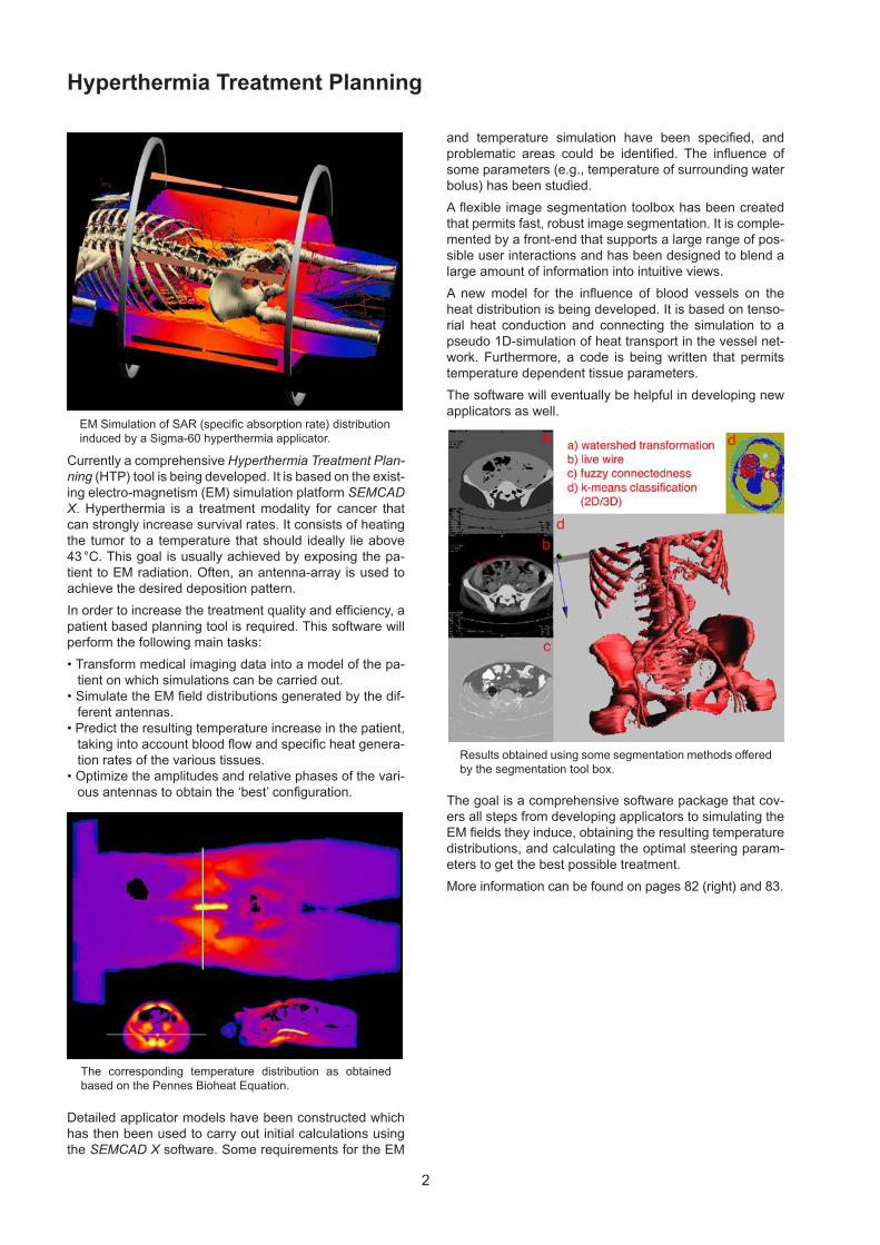
Currently a comprehensive Hyperthermia Treatment Plan-ning (HTP) tool is being developed. It is based on the exist-ing electro-magnetism (EM) simulation platform SEMCAD X. Hyperthermia is a treatment modality for cancer that can strongly increase survival rates. It consists of heating the tumor to a temperature that should ideally lie above 43 °C. This goal is usually achieved by exposing the pa-tient to EM radiation. Often, an antenna-array is used to achieve the desired deposition pattern.
In order to increase the treatment quality and efficiency, a patient based planning tool is required. This software will perform the following main tasks:
• Transform medical imaging data into a model of the pa-tient on which simulations can be carried out.
• Simulate the EM field distributions generated by the dif-ferent antennas.
• Predict the resulting temperature increase in the patient, taking into account blood flow and specific heat genera-tion rates of the various tissues.
• Optimize the amplitudes and relative phases of the vari-ous antennas to obtain the ‘best’ configuration.
Detailed applicator models have been constructed which has then been used to carry out initial calculations using the SEMCAD X software. Some requirements for the EM
and temperature simulation have been specified, and problematic areas could be identified. The influence of some parameters (e.g., temperature of surrounding water bolus) has been studied.
A flexible image segmentation toolbox has been created that permits fast, robust image segmentation. It is comple-mented by a front-end that supports a large range of pos-sible user interactions and has been designed to blend a large amount of information into intuitive views.
A new model for the influence of blood vessels on the heat distribution is being developed. It is based on tenso-rial heat conduction and connecting the simulation to a pseudo 1D-simulation of heat transport in the vessel net-work. Furthermore, a code is being written that permits temperature dependent tissue parameters.
The software will eventually be helpful in developing new applicators as well.
The goal is a comprehensive software package that cov-ers all steps from developing applicators to simulating the EM fields they induce, obtaining the resulting temperature distributions, and calculating the optimal steering param-eters to get the best possible treatment.
More information can be found on pages 82 (right) and 83.
Hyperthermia Treatment Planning
EM Simulation of SAR (specific absorption rate) distribution induced by a Sigma-60 hyperthermia applicator.
The corresponding temperature distribution as obtained based on the Pennes Bioheat Equation.
Results obtained using some segmentation methods offered by the segmentation tool box.
3
Contents
Preface 7
Organization 10
Representative Figures 11
Staff 14
Former PhD Students 16
Academic Guests 20
Partners and Funding Agencies 22
Awards 28
Patents 29
History of the Integrated Systems Laboratory (IIS) 30
Research Projects: IC and System Design and Test 34Circuits and Systems for Wireless Communications 35Real-Time MIMO-OFDM Testbed 35MIMO Detection and Channel Decoding 36Medium Access Control for MIMO-OFDM Testbed 36MIMO-OFDM Transceiver Chip 37MIMO-OFDM Transceiver Chip: Frontend 37MIMO-OFDM Transceiver Chip: OFDM Modulator 38MIMO-OFDM Transceiver Chip: MMSE-OSIC Detector 38Implementation Aspects of Pseudo-Linear MIMO Detectors 39VLSI Implementation of Reduced-Complexity Maximum-Likelihood Algorithms for MIMO Systems 39Sphere Decoding with Resource Constraints 40Baseband Processing on a Reconfigurable Processor 40MIMO-OFDM Frequency Offset Estimation 41GALS System Design 41Side-Channel-Attack Secure Crypto-Hardware 42Clock Oscillator with Variable Period 42Low-Power VLSI Implementation of Hearing Aid Algorithms 43Adaptive Directional Microphone for Hearing Aids 43Low-Power Speech Enhancement through Spectral Sharpening in Hearing Aids 44A New Low-Power Multiplier for Low-Frequency Applications 44
Research Projects: Analog and Mixed-Signal Design 45High-Speed Pipelined A/D Converters in Deep-Submicron DMOS Technology 46Folding and Interpolating A/D Converters in Deep Submicron Technology 46Frequency Synthesis for Ultra-Wideband Systems 47High Frequency Quadrature Oscillators 47Quadrature Modulator and Transitional Loop for GSM/DCS Mobile Transmitters 48Co-Integration of DC-DC Conterters for Systems on Chip 48Multi-Standard RF Front-Ends for Mobile Communications 49A/D Conversion for Multi-Standard Wireless Receivers 49Multi-Standard Low-Power Base-Band Digital Receiver 50Testbed for the Base-Band Signal Processing Part of a Digital Receiver 50A Low-Power, Multi-Mode, Transmit I/Q Modulator in 0.13 mm CMOS 51Frequency Synthesizer for a UMTS Transceiver 51
Research Projects: Technology CAD 52Modeling of Post-CMOS Devices 53New One-Particle Monte Carlo Method 53Full-Band Formalism in Quantum Transport Modeling 54Scattering in Nanoscale Devices 54Rigorous Treatment of Coupled Modes in the NEGF Formalism 55Atomistic Simulation of Quantum Wire Based Transistors 55Application of the sp3d5s* Tight-Binding Method for the Bandstructure of Bulk, Quantum Well, and Quantum Wire 56The Harmonic Balance Approach in the Simulation of Semiconductor Devices 56Physics-Based Characterization of RF Transistors by Means of Harmonic Balance Simulations 57Harmonic Distortion in Quantum Well Edge-Emitting Lasers 57Robust and Efficient Solving Strategies for the Nonlinear One-Tone Harmonic Balance Equation 58
4
Codoping in Heavily n-doped Silicon 58Electrical Behavior of Alkali and Alkaline Earth Metals in Silicon 59Improvement of Diffusion and Activation Models by Ab Initio Simulations 59Robust Iterative Solvers in Nanoelectronic Computational Science 60Performance Issues of Spectral Preconditioners in Semiconductor Device Simulation 60
Research Projects: Computational Optoelectronics 61Analysis of Optical Gain in InGaN/GaN Quantum Wells 62Optical Waveguide Analysis of an Edge Emitting Semiconductor Laser Working in the Visible Spectrum 62Explanation of Threshold Shift with Ambient Temperature for a 980nm Power Laser 63Microscopic Modeling of Gain and Amplified Spontaneous Emission in Superluminescent LEDs 63Static and Dynamic Calibration of VCSELs 64Full 3D VCSEL Simulation 64Optical Power Spectrum under Current Modulation 65Dynamic Properties of Long-Wavelength Vertical Cavity Surface Emitting Lasers 65Simulation of 1.3 mm VCSELs with Tunnel Junction 663D FEM Maxwell Solver for Photonic Crystal Light Emitters 663D Electrothermo-Optical Simulation of Three-Section DBR Laser 67TE/TM Polarized Semiconductor Optical Amplifier with Multi Quantum Well Active Region 67Simulation and Fabrication of Electrically Pumped Ultrafast VECSELs 68Microscopic Investigation of Optical Properties in Quantized Semiconductor Nanostructures 68
Research Projects: Physical Characterization 69Development of an Experimental Setup for the Measurement of the Hall Bulk Mobility up to 1000 K 70Measurement of Hole Impact Ionization in Silicon at High Temperature 70Electrothermal Simulation and Calibration of the Hole Impact Ionization in Silicon at High Temperature 71Extending the Extraction of the Bulk Mobility in Lightly Doped Silicon Towards High Temperatures 71Investigation of the Imaging and of the Quantitative Performance of the Scanning Spreading Resistance Microscopy 72Comparing Scanning Probe Techniques for the Characterization of Power Semiconductors 72Characterization of the Degradation of IGBT Devices for Traction Applications during Field Operation 73Performance and Limitations in Accurate Electrothermal Compact Modeling of Power Modules 733D Device Simulation of Thyristors as CMOS ESD Protection Elements 74Scanning Capacitance Characterization of Ultra High Boron Implanted High-Voltage Superjunction Transistors 742D Dopant Profiling of SiC MOSFET Devices by Scanning Capacitance and Secondary Electron Dopant Contrast 753D TCAD and Lithography Tools for Analysis and Modeling of a 65 nm Flared Gate MOS 75TCAD Simulation for Product-Performance Oriented Process Tuning 76Inverse Narrow Width Effect Study by Means of 3D TCAD Simulations on a 65 nm Technology 76Performance Driven TCAD Process Optimization for a Quarter Micron Low Power Product 77Three-Dimensional Simulation and Cross-Talk Effects in Flash Memory Cells 77Determining “Charged Device Model” ESD Robustness of ICs with Circuit Simulation 78Lifetime Prediction of Power Devices on the Base of Mission Profiles 78
Research Projects: Bio-Electromagnetics and Electromagnetic Compatibility 79SAR Assessment in Layered Body Tissue in the Near- and Far-Field of Wireless Body Worn Devices 80Numerical Characterization of Dosimetric Near-Field Probes for the Frequency Range of 5-6 GHz 80Development of Anatomical CAD Models of Two Adults and Two Children 81New Conformal FDTD Scheme with User-Defined Geometric Precision 81Conformal Alternating Direction Implicit (ADI) FDTD Solver 82Hyperthermia Treatment Planning – A Detailed Study of the Sigma-60 Applicator 82A Tool for Simulating EM Induced Heat Distributions in Living Tissue 83A Flexible Toolbox for 3D Segmentation of Medical Image Data 83Simulation of MTE Under Real World Test Conditions 84RF and Dosemtric Compliance Testing of Implanted Pacemakers 84Linux Numerical Solver IA32 and EMT64 (iSolve) Integration with aXware Hardware 85High Resolution Interpolation at Arbitrary Interfaces in FDTD 85Effective FDTD Modelling of Very Thin Conductive Sheets without Additional Field Equations 86A New High Speed Gridding Approach Processing Local 3D Data Optimized for Large Cell Size Ratios 86A Python Scripting Based Framework for Optimization in EM Simulations 87Active Optical Sensor for Field Measurement in Time and Frequency Domain 87Galvanical Coupling Through the Human Body in Clinical Trial 88Measurements and Numerical Simulation for Human Body Characterization 88In vivo Experiments: Dosimetric Requirements 89Study of UMTS Base Station Like Exposure in Well Being and Cognitive Performance 89Rodent Toxicity/Carcenogenicity Studies on Cell Phone Radio Frequency Radiation in Reverberation Chambers 90Final Dosimetry of the PERFORM A Project 90Assessment Methods for Demonstrating Compliance with Safety Limits for General Mobile Transmitters 91Assessment Techniques for the Cumulative Exposure of Mobile Phones in Real Networks 91Assessing the Relative Impact of Factors that Influence RF Exposure for Mobile Phones 92
5
Education Program: Student Projects 93EWA Splat Rasterizer ASIC 96EWA Splat Rasterizer Board 96VLSI Implementation of the FingerMouse Algorithm 97JPEG2000 Encoder VLSI Implementation 97FPGA Pre-Processing for Image Processing System 98ARC - Activity Recognition Chip 98ASIC for Railway Signal Monitoring 99ASIC for Digital Energy Metering 99AES-Based Strong-Authentication Module 100Side-Channel-Attack Resistant Strong-Authentication Module 100DPA Attack Board 101Concurrent Error Detection 101Acoustic MIMO Communication 102Implementation Issues of Hybrid Soft/-Hardware MACs 102Driver Development for a MIMO-OFDM Testbed 103MIMO Channel Emulator 103VAMP Board: SoC Development and Test Environment 104Network-on-Chip Integration 104Lowest-Latency Multi-Channel Audio Compression/Decompression Algorithm 105Sigma-Delta Modulator for a Class-D Audio Amplifier 105High-Efficiency High-End Audio Power Amplifier 106Process Synchronization Methods for Prototyping Platforms 106A Low-Power Analog-to-Digital Converter for Ultra-Wideband Applications 107A Complex DS Modulator for GSM/EDGE Applications 107Design of a Phase Locked Loop for Ultra-Wideband Frequency Synthesis 108LNAs for a Multi-Standard Wireless Receiver 108Multi-Standard and Broadband CMOS LNAs for Wireless Receivers 109Turbo En-/Decoder for UMTS 109Active-RC Filters for ADSL Communication Systems 110High-Speed, Low Power Chip Interconnects in 0.13 mm CMOS 110A 1.2V CMOS Analog Multiplier – Evaluation of Two Multiplier Designs 111A Classical View of Quantum Entanglement 111Impact Ionization Rate Calculations for Device Simulation 1123D Modelling and Simulation of VCSELs 112Measurements of Optical Gain with the Hakki-Paoli Technique 113Simulation and Measurement of the Optical Spectrum of VCSELs 113Dependence of the Power Control Statistics of Mobile Phones upon the Environment and Movement 114
PhD Theses – Abstracts 115
Master Theses – Overview 120
Student Projects – Overview 121
Education at IIS 123
Lectures 125
IC Design Projects – Overview 128
Research Projects – Overview 130
Microelectronics Design Center (DZ) 133
Joint Research Cooperation with the IT’IS Foundation 136
Publications 137
Presentations 144
Equipment for Electronic Test and Physical Characterization 150
EDA and TCAD Software 152
Computer Equipment 154

7
Introduction
This is a report on the academic and research activities of the Integrated Systems Laboratory (IIS) and the Micro-electronics Design Center (DZ) at the Department of Infor-mation Technology and Electrical Engineering (D-ITET) of the Swiss Federal Institute of Technology in Zurich (ETH Zurich) for the year 2005.
The IIS staff includes three professors, six research as-sociates, eleven post docs, forty five (45) PhD students, three computer system administrators, six persons in ad-ministration, and six technicians.
Research topics in digital, mixed, and analog integrated circuit (IC) design range from sensitive sensor interfaces to GHz RF circuits on the analog side, over analog-to-digital converters to the digital field covering projects from low-power design methodologies to complex systems-on-a-chip (SoC). Technology CAD (TCAD), technology and device development, computational optoelectronics, physical characterization, and bio-electromagnetics com-plement the research fields of IIS towards professional tools for modeling and optimizing nanoelectronic and op-toelectronic devices and technologies in the deep-submi-cron and nanometer range as well as bio-electromagnetic systems.
Microelectronics Design Center
The Microelectronics Design Center, headed by Dr. H. Kaeslin, with four staff members, is a service organization of the Department of Information Technology and Elec-trical Engineering. It is closely co-operating with IIS and other D-ITET and ETH Zurich laboratories in their design research and teaching activities for VLSI, analog, and sys-tem electronics (see page 133).
Research Projects and Funding
Following the trends of earlier years, our co-operation with national and international partners is at the center of our activities. In 2005, nine new research projects started in the fields of complex digital systems on chip, semicon-ductor process and device development and simulation, computational optoelectronics, and bio-electromagnetics.Two of them are European research projects (funded by the Commission of the Euopean Union), one KTI (Swiss Commission for Technology and Innovation), one re-search projects funded by ETH Zurich, four SNF (Swiss National Science Foundation), and one research project funded by SER (Swiss State Secretariate for Education and Research).
Overall, IIS was involved in a total of 27 research projects. Two of them were EU projects funded by SER and EU, eleven by KTI, three by ETH Zurich, five by SNF, two by TOP NANO 21, one by SER, and three by industrial part-ners in Switzerland, Europe, and Japan.
A total of 27 job positions at IIS was financed by third-party projects, which, in relation to the ETH positions, is a sign of the quality of research performed by our staff.
PhD Students
In 2005, nine PhD students finished their doctoral thesis successfully. IIS offers an excellent and highly stimulating research environment that permits PhD students to work on very attractive topics and, nevertheless, to finish their
thesis in a comparatively short time. However, it is still an ambitious challenge to find very qualified PhD students from all over the world. We try the best to overcome this situation by an appropriate salary policy and by focusing the student activities on scientific work in order to reduce the administrative and educational overhead.
Analog and Mixed Signal Group
For the Analog and Mixed Signal Integrated Circuit Design (AMIC) Group of Prof. Huang, the year 2005 has shown a continuation of work around the group’s focus in the field of RF and base-band circuit design for telecommunica-tions applications.
In 2005 the main outcome of the group´s research efforts has been the publication of a WCDMA frequency synthe-sizer at a well known conference. The circuit has been implemented in 0.13 mm CMOS technology, has very low phase noise and consumes only 9.5 mW of power.
In 2005 the AMIC group has been partner in several Swiss and international projects with research focus in advanced circuit design for wireless applications and implementa-tion in deep-submicron CMOS technologies at the 130 nm node and beyond. The group´s spin-off company ACP has participated 2005 in the EU-project “End-to-End Reconfig-urability”, a big European effort to make wireless telecom-munication equipment more versatile and hence saving development cost.
IC and System Design and Test Group
The research on multi-antenna (MIMO) communications systems in close collaboration with the Communication Theory Group of Prof. Helmut Bölcskei is the major activ-ity of the digital design group. The real-time MIMO-OFDM Testbed, known as “ETH Testbed”, has further been ex-tended, and at the same time it served for the design of one of the fastest WLAN ASIC realizations today, a 4 x 4 Antenna, 192 Mbits/s transceiver. The fruitful collabora-tion on MIMO enabled the participation on a EU project (MASCOT), starting in January 2006, with ETH as largest partner.
Beside manyfold building blocks for MIMO systems, fur-ther activities of the group led to a Crypto ASIC making use of Globally-Asynchronous Locally-Synchronous (GALS) techniques for Differential-Power-Attack resistivity. Signal processing for battery-powerd circuits could be enhanced towards even lower power consumption.
Technology CAD Group
Research in the Device Physics Group became even more directed to atomistic-type device modeling. To simulate two-dimensional ultra-thin body (UTB) and three-dimensional nanowire (NW) transistors with non-uniform confinement potential, the coupled mode space method in the non-equilibrium Green’s function formalism was revis-ited in collaboration with Prof. Mark Lundstrom from Pur-due University, USA. At the atomic scale, band structure effects play an essential role. Therefore, a new tool was developed for the calculation of Si, GaAs, Ge, and InAs UTB and NW band structures with and without strain in the sp3d5s* nearest neighbor tight-binding approach (joint project with Prof. Gerhard Klimeck from Purdue Univer-sity, USA). A full-band quantum transport code was imple-
Preface
8
mented for NWs, where interface roughness, alloy disor-der, and strain are included. It can be applied to different semiconductor materials and arbitrary growth directions.
Important applications of the theory of the moments of the inverse scattering operator (MISO) of the Boltzmann equation, published in the SIAM Journal of Applied Math-ematics, were studied. A method based on the MISO to compute exact energy relaxation times for low and high electric fields was developed. Also based on the MISO, a new one-particle Monte Carlo method which allows to take into account generation-recombination processes as well as quantum correction self-consistently, was implemented in the SimnIC device simulator. A method alternative to the “hierarchical noise simulation” was proposed to compute RF noise characteristics based on a constant number of noise sources independently of the transport model used. The device simulator SimnIC was extended to 3D devices, and a new algorithm was implemented to enhance the com-putation of distribution functions at high carrier energies.
The group strongly participated in the EU-IST project SINANO (Silicon-based Nanodevices) with quantum-bal-listic and Monte Carlo simulations of future transistor struc-tures.
Activities in ab initio process simulation included the evalu-ation of possible codopants for n-type silicon. The goal was to find a strategy for the manufacturing of highly doped ul-tra shallow junctions used for the next generation silicon devices. A profound analysis of various alkali and alkaline earth metals and their behavior in conjunction with arsenic doping was conducted. Moreover, a software environment for ab initio molecular dynamics simulations was developed that will be used for the evaluation of various dopant diffu-sion parameters.
The harmonic balance module of the mixed-mode device simulator has been extended to support thermodynamic, hydrodynamic, and density gradient transport descriptions, as well as optoelectronic transport. Furthermore, the ro-bustness and efficiency of the solution algorithm has been improved by using physically motivated preconditioners for the linear iterative solver and by parallelizing parts of the iteration process, respectively.
The parallel iterative linear solver used in the device simu-lator has been improved further. The focus has shifted from performance to accuracy and robustness issues. Spectral preconditioners have been investigated and implemented in the iterative solver. These preconditioners are based on spectral information of the iteration matrix and significantly improve the accuracy of the solution.
Computational Optoelectronics Group
The COE group has focused on the design and model de-velopment of semiconductor optoelectronic devices. In the domain of nanoscale light emitters, projects have started that aim to model the physical properties of optical cavities with high quality factors in connection with quantum dots/wires and wells. These emitters are envisioned to approach ultrahigh efficiencies. In the area of Gallium-Nitride based blue lasers, we could demonstrate, for the first time, a quantitative microscopic model for optical gain, and explain the characteristic features of the electro-optic mechanisms. The comprehensive, commercial simulator for surface emitting lasers (VCSELs) has been extended to simulate three-dimensional structures, and a novel model for the dy-namic lineshape has been derived. In a collaboration with several industrial partners, various VCSEL designs have been calibrated with static and dynamic data, which built
the cornerstone for dedicated design studies. The devices were characterized in our OptoLab, which enabled a com-prehensive and complete set of data for model calibration. Design modifications resulting in high single-mode optical power as well as modulation bandwidth were achieved.
Physical Characterization Group
The European project DEMAND aimed to measure fun-damental physical parameters in silicon at very high tem-perature has been concluded very successfully. In this framework, the bulk and surface mobility as well as the impact ionization coefficients have been measured and modeled up to 975 K, 675 K, and 870 K, respectively. These temperature limits have been never reached before. The quantitative assessment of scanning probe techniques for two-dimensional doping profiling (in particular Scanning Capacitance and Scanning Spreading Resistance) has been completed and extended to the characterization of silicon power devices. A novel and original technique based on the mapping of the surface potential by secondary elec-tron potential profiling has been proposed for silicon car-bide and has found a wide acceptance in the physical char-acterization community. Transient interferometry mapping has been used successfully to extract parameters and to validate transient thermo-electrical simulations of ESD pro-tections. Further activities are going on in conjunction with Synopsys Switzerland LLC in the field for the development of 3D TCAD tools for the analysis and compact modeling of deep sub-micrometer MOS and for the development of a suitable TCAD environment for accurate 3D simulation of non-volatile memories. Finally, a new European project has been started in co-operation with a major European lo-comotive manufacturer, which focuses on the deployment of reliability growth strategies for IGBT devices for railway traction.
Bio-Electromagnetics Group
IT’IS, the “Foundation for Research on Information Tech-nologies in Society” (headed by ETH adjunct Prof. Niels Kuster), a non-profit research institution supported by ETH Zurich, established its scientific and technical work in close collaboration with our laboratory. The research activities of IT’IS are in the domain of the interaction of electromagnetic radiation with biological organisms, in advanced measure-ment equipment for electromagnetic radiation, and health risk assessment. A growing number of research projects and PhD students at IIS is funded by the global wireless communications industry, several governmental agencies, and the Commission of the European Union. It turned out that this collaboration with IT’IS is very fruitful and a benefit for both institutions (see page 136).
Education
Next to research, teaching occupies a central role in our ac-tivities. Our staff is responsible for several core lectures in Information Technology and Electrical Engineering as well as in other departments (see page 125). The chapter on stu-dent projects (page 93) gives an overview on the manifold diploma theses and semester projects. Several outstanding student projects contribute to our research projects. Their descriptions can be found together with the research re-ports on pages 36 (right), 37 (right), 38, 39 (right), 40 (left),36 (right), 37 (right), 38, 39 (right), 40 (left), 41 (left), 43 (right), 44 (left), 47 (right), 64 (right), and 66, 47 (right), 64 (right), and 66 (left), and often lead to accepted presentations at interna-tional conferences (references [D6, T2, O1, O3, O4, O11]; pages 137ff) or to journal contributions ([D1]).
9
Partners and Funding Agencies
The activities of our laboratory were only possible through the support from the governing board of our university, and several national and international institutions and industri-al parties. Special thanks go to our school, to the comput-ing services of ETH Zurich, as well as to the Department of Information Technology and Electrical Engineering and its services and administration.
Finally, we would like to express our gratitude to the Swiss Commission for Technology and Innovation (KTI), the Swiss National Science Foundation (SNF), the Swiss State Secretariate for Education and Research (SER), the Swiss program TOP NANO 21, and the Commission of the European Union for their financial support. Just as much we would like to thank our partners ACP, Albis Optoelectronics, Alstom France, austriamicrosystems Austria, Avalon Photonics Switzerland, BeamExpress Switzerland, Bernafon Switzerland, Bookham Switzer-land, Bosch Germany, BridgeCo Switzerland, CEA/LETI France, CNM Italy, EPFL Switzerland, Exalos Switzerland, Fraunhofer-Gesellschaft Germany, Fujitsu Japan, IBM Research Switzerland, IMEC Belgium, IMM Italy, Infineon Germany, IT’IS Foundation Switzerland, Miromico Swit-zerland, Philips Semiconductors Zurich Switzerland, Philips Research Belgium, Siemens Germany, SIGMA-C Germany, SPEAG Switzerland, ST Microelectronics Italy and France, Sunrise Switzerland, Synopsys Switzerland LLC, Toshiba Japan, Toyota Japan, Technical University Wien Austria, University of Basel Switzerland, University of Bern Switzerland, University of Bologna Italy, Univer-sity of Cagliari Italy, University of California Santa Barbara USA, University of Canberra Australia, University of Graz Austria, University of Linz Austria, University of Padova Italy, University of Pisa Italy, University of Purdue USA, University of Stanford USA, University of Yerevan Arme-nia, Austria, WIAS Germany, and the ETH Zurich labora-tories IfA, IfE, IFH, IKT, IQE, ISI, IWR, and MATH for the fruitful cooperation in research projects as well as for their financial support.
10
Org
anizatio
n
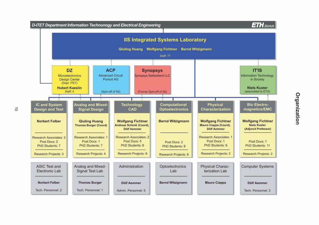
Administration
Dölf Aemmer
Admin. Personnel: 5
Computer Systems
Dölf Aemmer
Tech. Personnel: 3
ASIC Test andElectronic Lab
Norbert Felber
Tech. Personnel: 2
Analog and Mixed-Signal Test Lab
Thomas Burger
Tech. Personnel: 1
Optoelectronics Lab
Bernd Witzigmann
Physical Charac- terization Lab
Mauro Ciappa
DZMicroelectronicsDesign Center
(Dept. ITET)
Hubert KaeslinStaff: 4
IT'ISInformation Technology
in Society
Niels Kuster(associated to ETH)
IIS Integrated Systems LaboratoryQiuting Huang Wolfgang Fichtner Bernd Witzigmann
Staff: 77
SynopsysSynopsys Switzerland LLC
(Former Spin-off of IIS)
ACPAdvanced Circuit
Pursuit AG
(Spin-off of IIS)
ETH ZürichD-ITET Department Information Technonogy and Electrical Engineering
IC and SystemDesign and Test
Norbert Felber
Research Associates: 2Post Docs: 2
PhD Students: 7
Research Projects: 3
Analog and Mixed-Signal Design
Qiuting HuangThomas Burger (Coord)
Research Associates: 1Post Docs: 1
PhD Students: 7
Research Projects: 4
Technology CAD
Wolfgang FichtnerAndreas Schenk (Coord),
Dölf Aemmer
Research Associates: 2Post Docs: 5
PhD Students: 6
Research Projects: 9
Computational Optoelectronics
Bernd Witzigmann
Post Docs: 2PhD Students: 8
Research Projects: 8
Bio Electro-magnetics/EMC
Wolfgang FichtnerNiels Kuster
(Adjunct Professor)
Post Docs: 1PhD Students: 11
Research Projects: 2
Physical Characterization
Wolfgang FichtnerMauro Ciappa (Coord),
Dölf Aemmer
Research Associates: 1Post Docs: 1
PhD Students: 6
Research Projects: 2
11
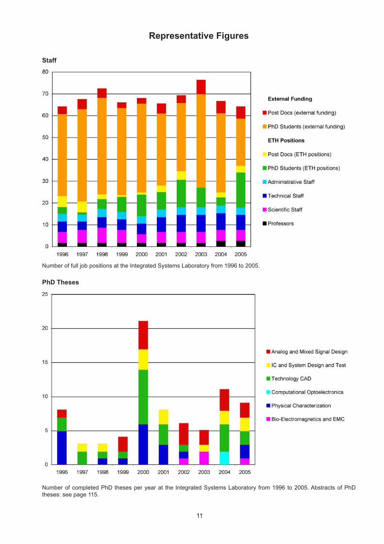
Representative Figures
Staff
Number of full job positions at the Integrated Systems Laboratory from 1996 to 2005.
PhD Theses
Number of completed PhD theses per year at the Integrated Systems Laboratory from 1996 to 2005. Abstracts of PhD theses: see page 115.
Journal and Book Publications
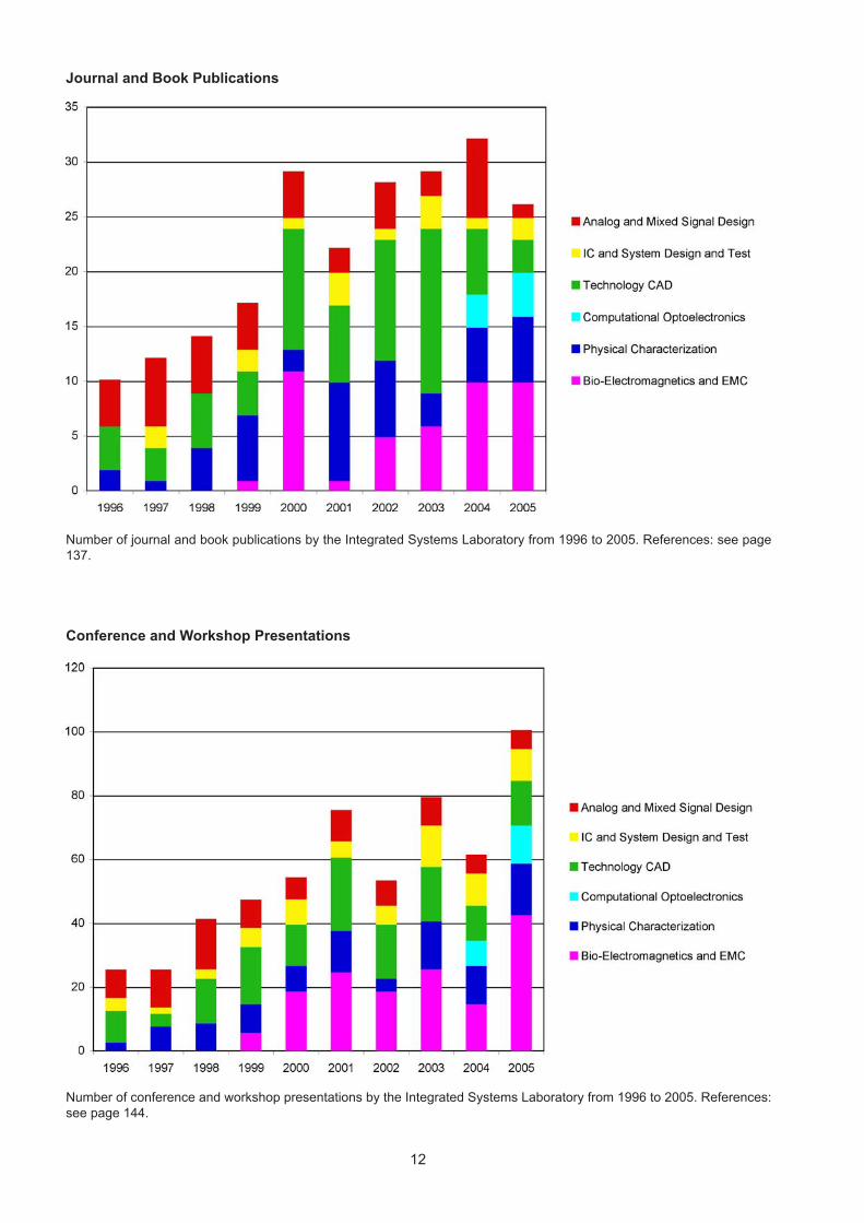
Number of journal and book publications by the Integrated Systems Laboratory from 1996 to 2005. References: see page 137.
Conference and Workshop Presentations
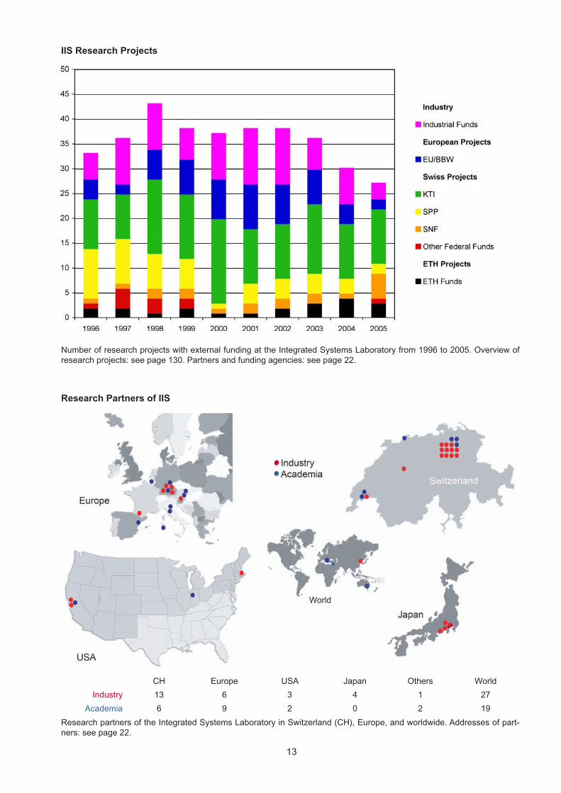
Number of conference and workshop presentations by the Integrated Systems Laboratory from 1996 to 2005. References: see page 144.
12
IIS Research Projects
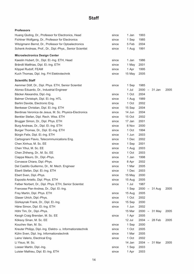
Number of research projects with external funding at the Integrated Systems Laboratory from 1996 to 2005. Overview of research projects: see page 130. Partners and funding agencies: see page 22.
Research Partners of IIS
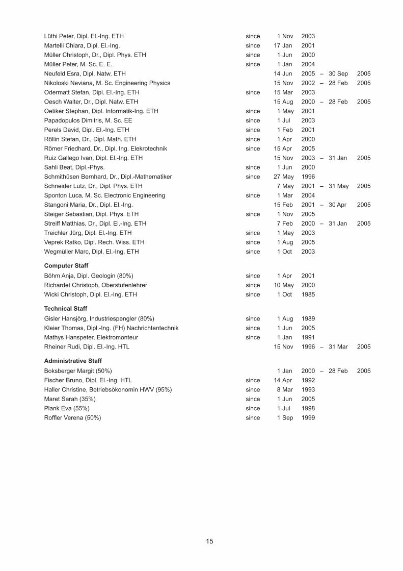
CH Europe USA Japan Others World
Industry 13 6 3 4 1 27
Academia 6 9 2 0 2 19
Research partners of the Integrated Systems Laboratory in Switzerland (CH), Europe, and worldwide. Addresses of part-ners: see page 22.
13
World
14
Professors
Huang Qiuting, Dr., Professor for Electronics, Head since 1 Jan 1993
Fichtner Wolfgang, Dr., Professor for Electronics since 1 Sep 1985
Witzigmann Bernd, Dr., Professor for Optoelectronics since 5 Feb 2004
Schenk Andreas, Prof., Dr., Dipl.-Phys., Senior Scientist since 1 Aug 1991
Microelectronics Design Center
Kaeslin Hubert, Dr., Dipl. El.-Ing. ETH, Head since 1 Jan 1986
Brändli Matthias, Dipl. El.-Ing. ETH since 1 May 2001
Köppel Rudolf, FEAM since 1 Apr 1995
Kuch Thomas, Dipl. Ing. FH Elektrotechnik since 15 May 2005
Scientific Staff
Aemmer Dölf, Dr., Dipl. Phys. ETH, Senior Scientist since 1 Sep 1985
Alonso Eduardo, Dr., Industrial Engineer 1 Jul 2000 – 31 Jan 2005
Bäcker Alexandra, Dipl.-Ing. since 1 Oct 2004
Balmer Christoph, Dipl. El.-Ing. HTL since 1 Aug 1989
Barlini Davide, Electronic Eng. since 1 Oct 2002
Benkeser Christian, Dipl. El.-Ing. ETH since 15 Sep 2004
Berdinas Veronica de Jesus, M. Sc. Physics-Electronics since 14 Jun 2004
Benkler Stefan, Dipl. Rech. Wiss. ETH since 15 Oct 2002
Brugger Simon, Dr., Dipl. Phys. ETH since 17 Jan 2001
Burg Andreas, Dr., Dipl. El.-Ing. ETH since 6 Nov 2000
Burger Thomas, Dr., Dipl. El.-Ing. ETH since 1 Oct 1994
Bürgin Felix, Dipl. El.-Ing. ETH since 1 Jun 2003
Carbognani Flavio, Telecommunications Eng. since 1 Dec 2002
Chen Xinhua, M. Sc. EE since 1 Sep 2001
Chen Yihui, M. Sc. EE since 1 Aug 2003
Chen Zhiheng, Dr., M. Sc. EE since 1 Oct 2003
Ciappa Mauro, Dr., Dipl.-Phys. since 1 Jan 1998
Corvasce Chiara, Dipl.-Phys. since 8 Apr 2002
Del Castillo Guillermo, Dr., M. Mech. Engineer since 1 Mar 2005
Eberli Stefan, Dipl. El.-Ing. ETH since 1 Dec 2003
Ebert Sven, Dipl.-Phys. since 15 May 2000
Esposito Aniello, Dipl. Phys. ETH since 15 Aug 2005
Felber Norbert, Dr., Dipl. Phys. ETH, Senior Scientist since 1 Jul 1987
Francese Pier-Andrea, Dr., Dipl. El.-Ing. 1 Sep 2000 – 31 Aug 2005
Frey Martin, Dipl. Phys. ETH since 15 Aug 2005
Glaser Ulrich, Dipl.-Phys. since 1 Oct 2002
Gürkaynak Frank, Dr., Dipl. El.-Ing. since 15 Sep 2000
Häne Simon, Dipl. El.-Ing. ETH since 1 Jun 2002
Höhr Tim, Dr., Dipl.-Phys. 15 Mar 2000 – 31 May 2005
Keogh Craig Brendan, M. Sc. EE since 1 Apr 2005
Köksoy Sinan, M. Sc. EE 12 Jul 2004 – 28 Feb 2005
Kouchev Ilian, M. Sc. since 1 Sep 2000
Kreuter Philipp, Dipl.-Ing. Elektro- u. Informationstechnik since 1 Oct 2005
Kühn Sven, Dipl. Ing. Informationstechnik since 1 Mar 2005
Laino Valerio, Electrical Eng. since 1 Oct 2002
Li Yisuo, M. Sc. 14 Jan 2004 – 31 Mar 2005
Loeser Martin, Dipl.-Ing. since 1 Sep 2003
Luisier Mathieu, Dipl. El.-Ing. ETH since 1 Apr 2003
Staff
15
Lüthi Peter, Dipl. El.-Ing. ETH since 1 Nov 2003
Martelli Chiara, Dipl. El.-Ing. since 17 Jan 2001
Müller Christoph, Dr., Dipl. Phys. ETH since 1 Jun 2000
Müller Peter, M. Sc. E. E. since 1 Jan 2004
Neufeld Esra, Dipl. Natw. ETH 14 Jun 2005 – 30 Sep 2005
Nikoloski Neviana, M. Sc. Engineering Physics 15 Nov 2002 – 28 Feb 2005
Odermatt Stefan, Dipl. El.-Ing. ETH since 15 Mar 2003
Oesch Walter, Dr., Dipl. Natw. ETH 15 Aug 2000 – 28 Feb 2005
Oetiker Stephan, Dipl. Informatik-Ing. ETH since 1 May 2001
Papadopulos Dimitris, M. Sc. EE since 1 Jul 2003
Perels David, Dipl. El.-Ing. ETH since 1 Feb 2001
Röllin Stefan, Dr., Dipl. Math. ETH since 1 Apr 2000
Römer Friedhard, Dr., Dipl. Ing. Elekrotechnik since 15 Apr 2005
Ruiz Gallego Ivan, Dipl. El.-Ing. ETH 15 Nov 2003 – 31 Jan 2005
Sahli Beat, Dipl.-Phys. since 1 Jun 2000
Schmithüsen Bernhard, Dr., Dipl.-Mathematiker since 27 May 1996
Schneider Lutz, Dr., Dipl. Phys. ETH 7 May 2001 – 31 May 2005
Sponton Luca, M. Sc. Electronic Engineering since 1 Mar 2004
Stangoni Maria, Dr., Dipl. El.-Ing. 15 Feb 2001 – 30 Apr 2005
Steiger Sebastian, Dipl. Phys. ETH since 1 Nov 2005
Streiff Matthias, Dr., Dipl. El.-Ing. ETH 7 Feb 2000 – 31 Jan 2005
Treichler Jürg, Dipl. El.-Ing. ETH since 1 May 2003
Veprek Ratko, Dipl. Rech. Wiss. ETH since 1 Aug 2005
Wegmüller Marc, Dipl. El.-Ing. ETH since 1 Oct 2003
Computer Staff
Böhm Anja, Dipl. Geologin (80%) since 1 Apr 2001
Richardet Christoph, Oberstufenlehrer since 10 May 2000
Wicki Christoph, Dipl. El.-Ing. ETH since 1 Oct 1985
Technical Staff
Gisler Hansjörg, Industriespengler (80%) since 1 Aug 1989
Kleier Thomas, Dipl.-Ing. (FH) Nachrichtentechnik since 1 Jun 2005
Mathys Hanspeter, Elektromonteur since 1 Jan 1991
Rheiner Rudi, Dipl. El.-Ing. HTL 15 Nov 1996 – 31 Mar 2005
Administrative Staff
Boksberger Margit (50%) 1 Jan 2000 – 28 Feb 2005
Fischer Bruno, Dipl. El.-Ing. HTL since 14 Apr 1992
Haller Christine, Betriebsökonomin HWV (95%) since 8 Mar 1993
Maret Sarah (35%) since 1 Jun 2005
Plank Eva (55%) since 1 Jul 1998
Roffler Verena (50%) since 1 Sep 1999
16
Name Year Now with
Bach Carlo 1993 Interstaatliche Hochschule für Technik (NTB) Werdenbergstrasse 4, CH-9471 Buchs, Switzerland
Balmelli Pio 2003 Silicon Laboratories 7000 West William Cannon Drive, Bldg. 1, Austin, TX 78735, USA
Basedau Philipp 1999 Philips Semiconductors AG Binzstrasse 44, CH-8045 Zürich, Switzerland
Bonnenberg Heinz 1993 Micronas GmbH Frankenthalerstrasse 2, D-81539 München, Germany
Bösch Thomas 2004 STMicroelectronics N.V. Via Cantonale 16 E, CH-6928 Manno, Switzerland
Brenna Gabriel 2004 Roswiesenstrasse 171, CH-8051 Zürich
Brugger Simon 2005 Integrated Systems Laboratory, ETH Zürich CH-8092 Zürich, Switzerland
Burg Andreas 2005 Integrated Systems Laboratory, ETH Zürich CH-8092 Zürich, Switzerland
Burger Thomas 2002 Integrated Systems Laboratory, ETH Zürich CH-8092 Zürich, Switzerland
Bürgler Josef 1990 Hochschule Technik+Architektur Luzern Technikumstrasse 21, CH-6048 Horw, Switzerland
Chavannes Nicolas 2002 IT’IS Foundation Zeughausstrasse 43, CH-8004 Zürich, Switzerland
Christ Andreas 2003 IT’IS Foundation Zeughausstrasse 43, CH-8004 Zürich, Switzerland
Ciampolini Lorenzo 2001 STMicroelectronics, Front-End Technology and Manufacturing 850, Rue Jean Monnet - BP16, F-38926 Crolles Cedex
Ciappa Mauro 2000 Integrated Systems Laboratory, ETH Zürich CH-8092 Zürich, Switzerland
Conti Paolo 1991 Glasmalergasse 2, CH-8004 Zürich, Switzerland
Curiger Andreas 1993 Omnisec AG Rietstrasse 14, CH-8108 Dällikon, Switzerland
Deiss Armin 2002 Microtune, Inc., 2201 10th Street, Plano, TX 75074, USA
Dettmer Hartmut 1994 Infineon Technologies AG Siemensstrasse 2, A-9500 Villach, Austria
Doswald Daniel 2000 ATI Technologies (Europe) GmbH Keltenring 13, D-82041 Oberhaching, Germany
Eicher Simon 1996 ABB Semiconductors AG R&D Lb2, Fabrikstrasse 3, CH-5600 Lenzburg, Switzerland
Esmark Kai 2001 Infineon Technologies DAT LIB TI-ESD/Latch-up, Postfach 80 17 09, D-81609 München, Germany
Etherton Melanie 2005 Freescale Semiconductor, Inc. 3501 Ed Bluestein Blvd. MD:K10, Austin, TX 78721, USA
Fillo Marco 1993 Quadrics Supercomputers World Ltd. Via Marcellina 11, I-00131 Roma, Italy
Francese Pier-Andrea 2005 National Semiconductor GmbH, Data Conversion Systems Group Livry-Gargan-Str. 10, D-82256 Fürstenfeldbruck, Germany
Gappisch Steffen 1996 Philips Semiconductors AG Binzstrasse 44, CH-8045 Zürich, Switzerland
Garreton Gilda 1998 Sun Microsystems Laboratories Asynchronous Group, 16 Network Circle, Menlo Park, CA 94025, USA
Geelhaar Frank 2004 Advanced Micro Devices, Inc. Sunnyvale, CA 94088-3453, USA.
Gull Ronald 1996 Synopsys Switzerland LLC Affolternstrasse 52, CH-8050 Zürich, Switzerland
Former PhD Students
17
Gürkaynak, Frank 2005 Integrated Systems Laboratory, ETH Zürich CH-8092 Zürich, Switzerland
Hager Christian 2000 McKinsey & Company Alpenstrasse 3, CH-8065 Zürich, Switzerland
Hammerschmied Clemens 2000 Maxim Integrated Products 120 San Gabriel Drive, Sunnyvale, CA 94086, USA
Heeb Hansruedi 1989 Im Tiergarten 9, CH-8055 Zürich, Switzerland
Heinz Frederik 2004 Intel Corp., Design & Technology Solutions RA3-254, 2501 NW 229th Ave., Hillsboro, OR 97124, USA
Heiser Gernot 1991 School of Computer Science & Engineering, University of New South Wales P.O. Box 1, Sydney, 2052 NSW, Australia
Herkersdorf Andreas 1991 TU München, Institute for Integrated Systems Arcisstr. 21, D-80290 München, Germany
Herrigel Alexander 1990 Bergstrasse 62, CH-8706 Meilen, Switzerland
Hertle Jürgen 2004 Photonfocus AG Bahnhofplatz 10, CH-8853 Lachen
Heusler Lucas 1990 IBM Zurich Research Division Zurich Research Laboratory, Säumerstrasse 4, CH-8803 Rüschlikon, Switzerland
Hitschfeld Nancy 1993 Departamento de Ciencias de la Computación, Universidad Católica de Chile Blanco Encalada 2120, Santiago, Chile
Höfler Alexander 1997 Freescale Semiconductor Inc. 6501 West William Cannon Drive, Mail Drop OE341, Austin, TX 78735, USA
Höhr Timm 2005 Infineon Technologies Dresden TC FL 3, Königsbrücker Strasse 180, D-01099 Dresden, Germany
Humbel Oliver 2000 Infineon Technologies Austria AG AI PL T PI 32 HV, Siemensstrasse 2, A-9500 Villach, Austria
Kells Kevin 1994 Synopsys, Inc. 700 East Middlefield Road, Mountain View, CA 94043, USA
Körner Thomas 1999 ABB Business Services Ltd. SLE-I Intellectual Property, Brown Boveri Strasse 6, CH-5400 Baden, Switzerland
Krause Jens 2001 Möllingstrasse 13, D-24103 Kiel, Germany
Krumbein Ulrich 1996 Infineon Technologies WS SD D Tr MOS, Postfach 80 09 49, D-81609 München, Germany
Kuratli Christoph 1999 Bernafon AG IC-Design, Morgenstrasse 131, CH-3018 Bern, Switzerland
Lamb Peter 1990 55 Gilbert ST, Hackett 2602, Canberra, Australia
Lendenmann Heinz 1994 ABB Corporate Research Dept. G, SE-721 78 Västerås, Sweden
Leonhardt Götz 2000 Synopsys, Inc. 700 East Middlefield Road, Mountain View, CA 94043, USA
Liegmann Arno 1995 Rüti 18, CH-8357 Guntershausen, Switzerland
Litsios James 1996 Actant AG Bahnhofstrasse 10, CH-6300 Zug, Switzerland
Menolfi Christian 2000 IBM Zurich Research Laboratory Säumerstrasse 4, CH-8803 Rüschlikon, Switzerland
Mergens Markus 2001 Infineon Technologies AIM AP D TD M1, P.O. Box 80 09 49, D-81609 München, Germany
Müller Christoph 2004 Integrated Systems Laboratory, ETH Zürich CH-8092 Zürich, Switzerland
Müller Stephan 1994 371 Maeve Court, San Jose, CA 95136, USA
Muttersbach Jens 2001 Philips Semiconductors AG Räffelstrasse 29, 8045 Zürich, Switzerland
Neeracher Matthias 1998 Apple Computer, Inc. MS 302-2LF, 1 Infinite Loop, Cupertino, CA 95014, USA
Nussbaum Miguel 1988 Departamento de Ciencias de la Computación, Universidad Católica de Chile Casilla 6177, Santiago, Chile
Oesch Walter 2005 Ammann Aufbereitung AG Eisenbahnstrasse 25, CH-4901 Langenthal, Switzerland

18
Oberle Michael 2002 IT’IS Zeughausstrasse 43, CH-8004 Zürich, Switzerland
Omura Ichiro 2001 Toshiba Corp. Semiconductor Comp. Discrete Semiconductor Division 1, Komukai Toshiba-cho, Saiwai-ku, Kawasaki 212-8583, Japan
Orsatti Paolo 2000 NemeriX SA Stabile Gerre 2000, Casella postale 425, CH-6928 Manno, Switzerland
Pfaff Dirk 2003 Diablo Technologies Inc. 290 Boulevard St-Joseph, Suite 200, Gatineau, Quebec, J8Y 3Y3, Canada
Pfäffli Paul 1999 Synopsys Switzerland LLC Affolternstrasse 52, CH-8050 Zürich, Switzerland
Pfeiffer Michael 2004 Synopsys Switzerland LLC Affolternstrasse 52, CH-8050 Zürich, Switzerland
Piazza Francesco 2000 NemeriX SA Stabile Gerre 2000, Casella postale 425, CH-6928 Manno, Switzerland
Pommerell Claude 1992 ABB (Switzerland) Ltd. CH-I Information Technology, Brown Boveri Strasse 6, CH-5400 Baden, Switzerland
Rogenmoser Robert 1996 Broadcom Corporation Broadband Processor Business Unit, 2451 Mission College Boulevard, Santa Clara, CA 95054, USA
Rogin Jürgen 2004 Advanced Circuit Pursuit AG Zwischenweg 2, CH-8702 Zollikon, Switzerland
Röllin Stefan 2004 Integrated Systems Laboratory, ETH Zürich CH-8092 Zürich, Switzerland
Roth Eric 2004 Esmertec AG Lagerstrasse 14, CH-8600 Dübendorf, Switzerland
Rothacher Fritz 1995 Infineon Technologies Communication Solutions, Am Campeon 1-12, D-85579 Neubiberg, Germany
Röwer Thomas 2000 1 Pilgrim Drive, Danbury, CT 06811, USA
Rühl Roland 1992 PDF Solutions, Inc. 333 West San Carlos Street, San Jose, CA 95110, USA
Ryter Roland 1996 Philips Semiconductors AG B137, Binzstrasse 44, CH-8045 Zürich, Switzerland
Schenk Olaf 2000 Department of Computer Science, University of Basel Klingelbergstrasse 50, CH-4056 Basel, Switzerland
Schenkel Michael 2002 Synopsys Switzerland LLC Affolternstrasse 52, CH-8050 Zürich, Switzerland
Schmithüsen Bernhard 2001 Integrated Systems Laboratory, ETH Zürich CH-8092 Zürich, Switzerland
Scholze Andreas 2000 Synopsys, Inc. 700 East Middlefield Road, Mountain View, CA 94043, USA
Schönbächler Edgar 1998 Bien-Air Dental SA Länggasse 60, Case Postale 6008, CH-2500 Bienne 6, Switzerland
Schuderer Jürgen 2003 ABB Corporate Research Applied Physics & Materials, Segelhof 1, CH-5405 Baden-Dättwil, Switzerland
Schuster Christian 2000 IBM T. J. Watson Research Center Rt. 134, P.O. Box 218, Yorktown Heights, NY 10598, USA
Seda Steven 1993 Zurich Financial Services Mythenquai 2, CH-8022 Zürich, Switzerland
Stadler Manfred 2000 BridgeCo AG Ringstrasse 14, CH-8600 Dübendorf, Switzerland
Stangoni Maria 2005 Spitalstrasse 15, 8902 Urdorf, Switzerland
Streiff Matthias 2004 Sensirion AG Laubisruetistrasse 50, CH-8712 Stäfa, Switzerland
Stricker Andreas 2000 IBM Microelectronics MS 972C, 1000 Riverstreet, Essex Junction, VT 05452, USA
Thalheim Jan 2003 CT-Concept Technologie AG J. Renfer-Strasse 15, CH-2504 Biel, Switzerland
Thalmann Markus 2000 BridgeCo AG Ringstrasse 14, CH-8600 Dübendorf, Switzerland

19
Tschopp David 2005 Integrated Systems Laboratory, ETH Zürich CH-8092 Zürich, Switzerland
Villablanca Luis 2000 Synopsys, Inc. 700 East Middlefield Road, Mountain View, CA 94043, USA
Villiger Thomas 2004 Philips Semiconductors AG Binzstrasse 44, CH-8045 Zürich, Switzerland
von Arx Christoph 1996 cva technical consulting ag Geissfluhweg 30, CH-4600 Olten, Switzerland
Wassner Jürgen 2001 Schmid Telecom AG Binzstrasse 35, CH-8045 Zürich, Switzerland
Westermann Marc 1995 Logismata AG Hardturmstrasse 76, CH-8005 Zürich, Switzerland
Wettstein Andreas 2000 Synopsys Switzerland LLC Affolternstrasse 52, CH-8050 Zürich, Switzerland
Wikström Tobias 2000 ABB Switzerland Ltd., Semiconductors Fabrikstrasse 3, CH-5600 Lenzburg, Switzerland
Witzig Andreas 2002 Hochschule für Technik Rapperswil Solartechnik Prüfung Forschung, Oberseestrasse 10, CH-8640 Rapperswil, Switzerland
Witzigmann Bernd 2000 Integrated Systems Laboratory, ETH Zürich CH-8092 Zürich, Switzerland
Yun Chan-Su 2000 Synopsys, Inc. 700 East Middlefield Road, Mountain View, CA 94043, USA
Zahir Rumi 1991 428 Glenwood Avenue, Menlo Park, CA 94025, USA
Zelenka Stefan 2001 Synopsys Switzerland LLC Affolternstrasse 52, CH-8050 Zürich, Switzerland
Zimmermann Reto 1997 Synopsys Switzerland LLC Affolternstrasse 52, CH-8050 Zürich, Switzerland
20
Prof. Jacob Katzenelson Technion, Israel Institute of Technology, Haifa, Israel 1 Jan – 31 Mar 2005
Prof. Giorgio Baccarani Universita degli Studi di Bologna, Bologna, Italy 12 Jan 2005
Prof. Massimo Rudan Universita degli Studi di Bologna, Bologna, Italy 12 Jan 2005
Elena Gnani Universita degli Studi di Bologna, Bologna, Italy 12 Jan 2005
Susanna Reggiani Universita degli Studi di Bologna, Bologna, Italy 12 Jan 2005
Dr. Matthias Stecher Infineon Technologies AG, Munich, Germany 12 Jan 2005
Marie Denison Infineon Technologies AG, Munich, Germany 12 Jan 2005
Michael Mayerhofer Infineon Technologies AG, Munich, Germany 12 Jan 2005
Prof. Gerhard Groos Bundeswehr Universität, Munich, Germany 12 Jan 2005
Sergey Bychikhin TU Wien, Vienna, Austria 12 Jan 2005
Dr. Dionyz Pogany TU Wien, Vienna, Austria 12 Jan 2005
Prof. Gaudenzio Meneghesso Universita degli Studi di Padova, Padova, Italy 12 Jan 2005
Dr. Axel Erlenbach Synopsys Switzerland LLC, Zurich, Switzerland 12 Jan 2005
Dr. Michael Schenkel Synopsys Inc., Mountain View, CA, USA 12 Jan 2005
Dr. Antonio Andreini ST Microelctronics Sr1, Cornaredo, Italy 21 Feb – 22 Feb 2005
Tilo Brodbeck Infineon Technologies, Munich, Germany 21 Feb – 22 Feb 2005
Sergey Bychikhin TU Wien, Vienna, Austria 21 Feb – 22 Feb 2005
Lorenzo Cerati STMicroelectronics Srl, Agrate Brianza, Italy 21 Feb – 22 Feb 2005
Melanie Etherton Robert Bosch GmbH, Reutlingen, Germany 21 Feb – 22 Feb 2005
Markus Frank XFAB, Erfurt, Germany 21 Feb – 22 Feb 2005
Dr. Horst Gieser Fraunhofer Institut für Festkörpertech. IFT, Munich, Germany 21 Feb – 22 Feb 2005
Michael Graf Atmel Germany GmbH, Heilbron, Germany 21 Feb – 22 Feb 2005
Manfred Klaussner Atmel Germany GmbH, Heilbron, Germany 21 Feb – 22 Feb 2005
Ulrich Liebold IMMS GmbH, Erfurt, Germany 21 Feb – 22 Feb 2005
Prof. Gaudenzio Meneghesso University of Padova, Padova, Italy 21 Feb – 22 Feb 2005
Dr. Dionyz Pogany TU Wien, Vienna, Austria 21 Feb – 22 Feb 2005
Dr. Michael Schenkel Synopsys Inc., Mountain View, CA, USA 21 Feb – 22 Feb 2005
Dr. Theo Smedes Philips Semiconductors, Nijmegen, The Nederlands 21 Feb – 22 Feb 2005
Prof. Winfried Soppa Fachhochschule Osnabrück, Osnabrück, Germany 21 Feb – 22 Feb 2005
Dr. Wolfgang Stadler Infineon Technologies, Munich, Germany 21 Feb – 22 Feb 2005
Hans van Zwol Philips Semiconductors, Nijmegen, The Nederlands 21 Feb – 22 Feb 2005
Dr. Wolfgang Wilkening Robert Bosch GmbH, Reutlingen, Germany 21 Feb – 22 Feb 2005
Heinrich Wolf Fraunhofer Institut für Festkörpertech. IFT, Munich, Germany 21 Feb – 22 Feb 2005
Dr. Vito Raineri Italian National Council for Research, (IMM), Catania, Italy 22 Apr 2005
Prof. Erich Gornik TU Wien, Vienna, Austria 24 Feb – 25 Feb 2005
Prof. Massimo Rudan Universita degli Studi di Bologna, Bologna, Italy 25 Feb 2005
Markus Korn European Commission, Bruxelles, Begique 25 Feb 2005
Elena Gnani Universita degli Studi di Bologna, Bologna, Italy 25 Feb 2005
Susanna Reggiani Universita degli Studi di Bologna, Bologna, Italy 25 Feb 2005
Dr. Matthias Stecher Infineon Technologies AG, Munich, Germany 25 Feb 2005
Marie Denison Infineon Technologies AG, Munich, Germany 25 Feb 2005
Michael Mayerhofer Infineon Technologies AG, Munich, Germany 25 Feb 2005
Prof. Gerhard Groos Bundeswehr Universität, Munich, Germany 25 Feb 2005
Sergey Bychikhin TU Wien, Vienna, Austria 25 Feb 2005
Dr. Dionyz Pogany TU Wien, Vienna, Austria 25 Feb 2005
Dr. Axel Erlenbach Synopsys Switzerland LLC, Zurich, Switzerland 25 Feb 2005
Dr. M. Schenkel Synopsys Inc., Mountain View, CA, USA 25 Feb 2005
Dr. Ulrich Schwarz Universität Regensburg, Regensburg, Germany 14 Mar – 15 Mar 2005
Dr. Wei-Choon Ng Synopsys Inc., Mountain View, CA, USA 10 Mar 2005
Dr. Lorenzo Occhi Exalos AG, Zurich, Switzerland 10 Mar 2005
Academic Guests
21
Dr. Roland Raschke Fujitsu Laboratories of Europe, Darmstadt, Germany 22 Mar 2005
Dr. Ian Young Intel Corporation, Hilsboro, OR, USA 18 Apr 2005
Dr. Vito Raineri Italian National Council for Research, Catania, Italy 22 Apr 2005
Dr. Ran Ginosar VLSI Research Center, Technion, Haifa, Israel 26 Apr 2005
Dr. Paul Royo BeamExopress SA, Lausanne, Switzerland 2 Jun 2005
Dr. P. Altermann Institut für Festkörperphysik, Hannover, Germany 17 Jun 2005
Dr. Frederik Heinz Intel Corporation, Hilsboro, OR, USA 13 Jul 2005
Dr. Christian Vélez Exalos AG, Zurich, Switzerland 30 Jul 2005
Dr. Ian Aeby Emcore Corporation, Albuquerque, NM, USA 10 Aug 2005
Dr. Andreas Stricker IBM Microelectronics, Essex Junction, VT, USA 22 Aug 2005
Dr. Lorenzo Occhi Exalos AG, Zurich, Switzerland 7 Sep 2005
Hiromi Anzai Fujitsu Ltd., Atsugi, Japan 15 Sep 2005
Dr. Kiyoshi Ishikawa Renesas Technology Corp., Hyogo, Japan 15 Sep 2005
Makoto Isshiki Nihon Synopsys Co., Ltd., Tokyo, Japan 15 Sep 2005
Dr. Seiji Takahashi Sony Corporation, Kanagawa, Japan 15 Sep 2005
Wonchul Chul Nihon Synopsys Co., Ltd., Tokyo, Japan 15 Sep 2005
Prof. Giorgo Baccarani Universita degli Studi di Bologna, Bologna, Italy 26 Sep 2005
Prof. Hovik Baghdasaryan University of Armenia, Yerevan, Armenia 16 Nov – 18 Nov 2005
Dr. Wolfgang Stadler Infineon Technologies, Munich, Germany 21 Nov 2005
Dr. Wolfgang Wilkening Robert Bosch GmbH, Reutlingen, Germany 21 Nov 2005
Prof. Yusuf Leblebici Institut de Microélectronique et de Microsystèmes, EPFL Lausanne,
Switzerland 22 Nov 2005
Dr. Kunihiro Suzuki Fujitsu Laboratories Ltd., Atsugi, Japan 11 Dec – 16 Dec 2005
Prof. Markus Rupp TU Wien, Institut für Nachrichtentechnik und Hochfre-
quenztechnik, Vienna, Austria 19 Dec 2005
Prof. Massimo Macucci Universita di Pisa, Pisa, Italy 23 Dec 2005
22
ACP ACP Advanced Circuit Pursuit AG Alte Landstrasse 101, CH-8702 Zollikon ZH, Switzerland
Albis Optelectronics Albis Optoelectronics AG Moosstrasse 2, CH-8803 Rüschlikon, Switzerland
Alstom Alstom Transport S.A. 3 avenue André Malraux, F-92300 Levallois-Perret, France
and
Alstom Transport Composants Rue du Docteur Guinier - BP 4, F-65600 Semeac, France
AMAT Applied Materials, Inc. 974 E. Arques Avenue, M/S 81157, Sunnyvale, CA 94086, USA
austriamicrosystems austriamicrosystems AG Schloss Premstätten, A-8141 Unterpremstätten, Austria
Avalon Avalon Photonics Badenerstrasse 569, CH-8048 Zürich, Switzerland
BBT Bundesamt für Berufsbildung und Technologie (Federal Office for Professional Education and Technology, a Swiss Government Agency) Effingerstrasse 27, CH-3003 Bern, Switzerland
BBW Bundesamt für Bildung und Wissenschaft (Federal Office for Education and Science, a Swiss Government Agency) Wildhainweg 9, CH-3001 Bern, Switzerland
BeamExpress Beam Express PSE Bâtiment C, Ch-1015 Lausanne, Switzerland
Bernafon Bernafon AG Morgenstrasse 131, CH-3018 Bern, Switzerland
Bookham Bookham (Switzerland) AG Binzstrasse 17, CH-8045 Zürich, Switzerland
Bosch Robert Bosch GmbH Tübingerstrasse 123, D-72703 Reutlingen, Germany
and
Robert Bosch GmbH Wernerstrasse 1, D-70442 Stuttgart, Germany
BridgeCo BridgeCo AG Ringstrasse 14, CH-8600 Dübendorf, Switzerland
CNM Centro Nacional de Microelectrónica Campus Universidad Autónoma de Barcelona, E-08193 Bellaterra (Barcelona), Spain
E2R Consortium Motorola SAS, Gif sur Yvette, France ACP Advanced Circuit Pursuit AG, Zollikon, Switzerland Alcatel SEL AG, Stuttgart, Germany DICE Danube Integrated Circuit Engineering GmbH, Linz, Austria Dir. Gén. de l’Industrie des Technologies de l’Information et des Postes, Paris, France DoCoMo Communications Laboratories Europe GmbH, München, Germany Institut Eurecom, Sophia-Antipolis, France France Telecom SA, Paris, France Institute for Infocomm Research, Singapore, Singapore King’s College London, London, United Kingdom Mitsubishi Electric Information Technology Center Europe SARL, Rennes, France Nokia GmbH, Bochum, Germany Panasonic European Laboratories GmbH, Langen, Germany Panasonic Mobile Communications Development Laboratory, Uxbridge, United Kingdom Radiocommunications Agency, London, United Kingdom Regulierungsbehörde für Telekommunikation und Post, Mainz, Germany Siemens AG, München, Germany Siemens Mobile Communications SpA, Milano, Italy Telecom Italia SpA, Milano, Italy Telefonica Investigacion Y Desarrollo SAU, Madrid, Spain Thales Communications SA, Colombes, France Toshiba Research Europe Ltd, Cambridge, United Kingdom
Partners and Funding Agencies
23
E2R Consortium National Kapodistrian University of Athens, Athen, Greece Technische Universität Dresden, Dresden, Germany Universität Karlsruhe, Karlsruhe, Germany University of Piraeus Research Center, Piräus, Greece The University of Surrey, Guilford, United Kingdom Universitat Politecnica de Catalania, Barcelona, Spain Motorola Israel Ltd, Tel-Aviv, Israel
EPFL Ecole Polytechnique Fédéral Lausanne (Swiss Federal Institute of Technology Lausanne) CH-1015 Lausanne, Switzerland
ETHZ Eidgenössische Technische Hochschule Zürich (Swiss Federal Institute of Technology Zürich) ETH Zentrum, CH-8092 Zürich, Switzerland
Exalos Exalos AG Technoparkstrasse 1, CH-8005 Zürich, Switzerland
FhG-IISB Fraunhofer-Gesellschaft zur Förderung der angewandten Forschung e.V. Institut für Integrierte Schaltungen und Bauelementetechnologie Schottkystrasse 10, D-91058 Erlangen, Germany
Fujitsu Fujitsu Laboratories Ltd 10-1, Morinosato-Wakamiya, Atsugi 243-01, Japan
and
Fujitsu Laboratories of Europe Ltd Hayes Park Central, Hayes End Road, Hayes, Middlesex UB4 8FE, United Kingdom
IBM Research IBM Research GmbH Säumerstrasse 4, CH-8803 Rüschlikon, Switzerland
IEF Paris Université Paris Sud Bâtiment 510, F-91405 Orsay, France
IfA-ETHZ Institut für Automatik (Automatic Control Laboratory) ETH Zürich, Physikstrasse 3, CH-8092 Zürich, Switzerland
IfE-ETHZ Institut für Elektronik (Laboratory for Electronics) ETH Zürich, Gloriastrasse 35, CH-8092 Zürich, Switzerland
IfH-ETHZ Institut für Feldtheorie und Höchstfrequenztechnik (Laboratory for Electromagnetic Fields and Microwaves) ETH Zürich, Gloriastrasse 35, CH-8092 Zürich, Switzerland
IIS-ETHZ Integrated Systems Laboratory ETH Zürich, Gloriastrasse 35, CH-8092 Zürich, Switzerland (i.e. the publisher of this “Research Review 2005”)
IKT-ETHZ Institut für Kommunikationstechnik (Laboratory for Communication Technology) ETH Zürich, Sternwartstrasse 7, CH-8092 Zürich, Switzerland
IMEC Interuniversity Microelectronics Centre Kapeldreef 75, B-3001 Leuven, Belgium
IMM Istituto di Metodologie e Technologie per la Microelettronica Stradale Primosole 50, I-95121 Catania, Italy
Infineon Infineon Technologies AG Balanstrasse 73, D-81609 München, Germany
and
Infineon Technologies AG Siemensstrasse 2, A-9500 Villach, Austria
and
Infineon Technologies AG Am Campeon 1-12, D-85579 Neubiberg, Germany
IPEQ-EPFL Quantum Devices Group, Institut de Photonique et Electronique Quantique, Faculté Sciences de Base, EPFL, CH-1015 Lausanne (Switzerland)
IQE-ETHZ Institut für Quantenelektronik (Laboratory for Quantum Electronics) ETH Zürich, Wolfgang Pauli-Strasse 16 , CH-9093 Zürich, Switzerland
24
ISI-ETHZ Institut für Signal- und Informationsverarbeitung (Signal and Information Processing Laboratory) ETH Zürich, Gloriastrasse 35, CH-8092 Zürich, Switzerland
IT’IS IT’IS Foundation for Research on Information Technologies in Society ETHZ ETZ Gebäude, Gloriastrasse 35, CH-8006 Zürich, Switzerland
and
Zeughausstrasse 43, CH-8004 Zürich, Switzerland
IT’IS Partners Asher Sheppard Consulting, Redlands, USA ARCS, Seibersdorf (Austria) BAG, Bern (Switzerland) BASEXPO Consortium BfS, Salzgitter (Germany) BORL-USZ, Zürich (Switzerland) CTIA, Washington DC, (USA) EMPA, Dübendorf (Switzerland) Erasmus MC Rotterdam, Rotterdam (The Netherlands) Exponent Inc., Menlo Park, CA (USA) FAU Erlangen, Erlangen (Germany) FDA, Washington DC (USA) Fraunhofer ITEM, Hannover (Germany) GSM-Association, Genève (Switzerland) Guidant Corporation, St. Paul, MN (USA) IfW, St. Gallen (Switzerland) IMTEK, Freiburg (Germany) INTEC, Gent (Belgium) IPM, Stockholm (Sweden) IPT-UNIZH, Zürich (Switzerland) IZT, Berlin (Germany) Karolinska Institute, Huddinge (Sweden) KIST, Saarbrücken (Germany) MCL, London (Great Britain) MMF, Brussels (Belgium) Motorola, Ft. Lauderdale (USA) NIEHS, Research Triangle Park (USA) NIST, Gaithersburg (USA) NOKIA NRC, Helsinki (Finland) PERFORM A Consortium PERFORM B Consortium PERFORM C Consortium RCL/AUTH, Thessaloniki (Greece) SARSYS Consortium Siemens Medical Solutions AG, Erlangen (Germany) SRFMC, Zurich (Switzerland) TA SWISS, Bern (Switzerland) TDC, Zürich (Switzerland) ULP, Strasbourg (France) Uni Uppsala, Uppsala (Sweden) Uni Zürich, Zürich, (Switzerland) Zejiang University, Hangzhou (China)
IWR-ETHZ Institut für Wissenschaftliches Rechnen (Institute for Scientific Computing) ETH Zürich, Haldeneggsteig 4, CH-8092 Zürich, Switzerland
KTI Kommission für Technologie und Innovation (Commission for Technology and Innovation, a Swiss Government Agency) Effingerstrasse 27, CH-3003 Bern, Switzerland
LSM-EPFL Microelectronic Systems Laboratory, EPFL/STI-IMM-LSM Bldg ELD, Station 11, CH-1015 Lausanne, Switzerland
LPN-EPFL Laboratory of Physics of Nanostructures EPF Lausanne, CH-1015 Lausanne, Switzerland
Miromico Miromico AG Technoparkstrasse 1, CH-8005 Zürich, Switzerland
NEC NEC Corporation System Devices Research Laboratories 1120 Shimokuzawa, Sagamihara, 229-1198, Japan
25
Osram Osram Opto Semiconductors GmbH Wernerwerkstrasse 2, D-93049 Regensburg, Germany
Philips Zurich Philips Zürich AG, Semiconductors Binzstrasse 44, CH-8045 Zürich, Switzerland
PORTES Consortium Alstom Transport SA, Semeac, France Conseja Superior de Investigaciones Cientificas, Barcelona, Spain ETH Zürich, Zürich, Switzerland
PSI PSI Paul Scherrer Institut CH-5332 Villingen, Switzerland
SER Staatssekretariat für Bildung und Forschung (State Secretariat for Education and Research, a Swiss Government Agency) Hallwylstrasse 4, CH-3003 Bern, Switzerland
Samsung Samsung Electronics Co., LTD. San #24 Nongseo-Ri, Giheung-Eup, Yongin-City, Gyeonggi-Do,, Korea
Siemens Bocholt Siemens AG Information and Communication Mobile Frankenstrasse 2, D-46393 Bocholt, Germany
SINANO Consortium France Innovation Scientifique et Transfert S.A., FIST, Paris, France Centre National de la Recherche Scientifique, CNRS, Paris, France Technische Universität Wien - Institut für Festkörperelektronik, TUW FKE, Wien, Austria Technische Universität Wien - Institut für Mikroelektronik, TUW IME, Wien, Austria The University of Warwick, WARWICK, Coventry, United Kingdom Universite Catholique de Louvain, UCL, Louvain la Neuve, Belgium Rheinisch-Westfälische Technische Hochschule Aachen, RWTH, Aachen, Germany Alma Mater Studiorum - Universita di Bologna, ARCES, Bologna, Italy AMO GmbH, AMO, Aachen, Germany The University of Birmingham, BU, Birmingham, United Kingdom Commissariat a l’Energie Atomique, CEA, Paris, France Chalmers University of Technology AB, CHALMERS, Göteborg, Sweden Technische Universiteit Delft, DELFT, Delft, the Netherlands Ecole Polytechnique Federal de Lausanne, EPFL, Lausanne, Switzerland Eidgenössische Technische Hochschule Zürich, ETH, Zürich, Switzerland Forschungszentrum Juelich GmbH, FZJ JUELICH, Jülich, Germany The University of Glasgow, GLASGOW, Glasgow, United Kingdom Göteborgs Universitet, GOETEBORG, Göteborg, Sweden Universidad de Granada, GRANADA, Granada, Spain Fraunhofer-Gesellschaft E.V., IISB, Erlangen, Germany Interuniversitair Micro-Electronica Centrum VZW, IMEC, Leuven, Belgium National Center for Scientific Research “Demokritos”, IMEL, Aghia, Greece Infineon Technologies AG, INFINEON, München, Germany Kungliga Tekniska Högskolan, KTH, Stockholm, Sweden The University of Liverpool, LIVUNI, Liverpool, United Kingdom NMRC - University College of Cork, NMRC, Cork, Ireland University of Newscastle upon Tyne, NU, Newcastle upon Tyne, United Kingdom Universita degli Studi di Pisa - Dpt Ingegneeeria Dell Informazione, PISA, Pisa, Italy The University of Southampton, SOTTON, Southhampton, United Kingdom ST Microelectronics SA, ST, Montrouge, France Technische Universität München, TUM, München, Germany Linköpings Universitet - Institute of Technology, LINKOPING, Linköping, Sweden The University of Cambridge, UCAM, Cambridge, United Kingdom Universita degli Studi di Udine, UDINE, Udine, Italy Universitetsstudiene Pa Kjeller, UNIK, Kjeller, Norway Universitat Rovira i Virgili, URV, Tarragona, Spain Universität Stuttgart, USTUTT, Stuttgart, Germany Eberhard Karls Universität Tübingen, UTU, Tübingen, Germany Uppsala Universitet, UU, Uppsala, Sweden Politechnika Warszawska, WUT, Warszawa, Poland Institute of Semiconductor Physics - National Academy of Science, ISP, Kyiv, Ukraine Puslaidininkiu Fizikos Institutas, SPI, Vilnius, Lithuania
SNF Swiss National Science Foundation Wildhainweg 20, CH-3012 Bern, Switzerland
SPEAG Schmid & Partner Engineering AG Zeughausstrasse 43, CH-8004 Zürich, Switzerland
26
Sunrise Sunrise TDC Switzerland Thurgauerstrasse 60, CH-8050 Zürich, Switzerland
SUGERT Consortium Fraunhofer Gesellschaft E.V. IISB, Erlangen, Germany austriamicrosystems AG, Unterpremstätten, Austria Infineon Technologies AG, München, Germany Philips Innovative Technology Solutions NV, Heeverlee, Belgium ST-Microelectronics S.A., Crolles, France ST-Microelectronics SRL, Agrate Brianza, Italy SynopsysSwitzerland LLC, Zürich, Switzerland SIGMA-C GmbH Software, München, GermanySIGMA-C GmbH Software, München, Germany Commissariat a l’Energie Atomique/LETI, Grenoble, France Interuniversity Micro Electronic Center VZW, Leuven, Belgium ETH Zürich, Zürich, Switzerland Technische Universität Wien, Wien, Austria
Synopsys Synopsys Switzerland LLC Affolternstrasse 52, CH-8050 Zürich, Switzerland
and
Synopsys Inc. 700 East Middlefield Road, Mountain View, CA 94043, USA
TOP NANO 21 Swiss Technology Oriented Program NANO 21 Universität Basel Institut für Physik Klingelbergstrasse 82, CH-4056 Basel, Switzerland
and
Themas AG Egnacherstrasse 69, CH-9320 Arbon, Switzerland
Toshiba Toshiba Corporation 1-1. Shibaura 1-chome, Minato-ku, Tokyo 105-8001, Japan
and
Toshiba Corporation 2-5-1, Kasama, Sakae-ku, Yokohama 247-8585, Japan
and
Toshiba Corporation 1, Komukai, Toshibacho, Saiwai-ku, Kawasaki 210, Japan
Toyota Toyota Central R&D Labs. Inc. Nagakute-cho, Aichi-gun, Aichi 480-1192, Japan
TU Graz Technische Universität Graz Institute for Applied Information Processing and Communications (IAIK) Infeldgasse 16a, A-8010 Graz, Austria
TU München Technische Universität München Walter Schottky Institut Am Coulombwall 3, D-85748 Garching, Germany
TU Wien Technische Universität Wien Institute for Microelectronics Gusshausstrasse 27–29, A-1040 Wien, Austria
UCSB University of California ECE Department Santa Barbara, CA 93106-9560, USA
Uni Armenia State Engineering University of Armenia Fiber Optics Communication Laboratory 105 Terian Strasse, Yerevan 375009, Armenia
Uni Basel Universität Basel Departement für Computer Wissenschaften CH-4000 Basel, Switzerland
Uni Bern Universität Bern Universitätsklinik Inselspital CH-3010 Bern, Switzerland
Uni Bologna Universita degli Studi di Bologna Dipartimento di Elettronica Informatica e Sistemistica Via Zamboni 33, I-40126 Bologna, Italy

27
Uni Cagliari Universita degli Studi di´Cagliari Dipartimento di Ingegneria Elletrica et Elettronica Piazza D‘ armi, I-09123 Cagliari, Italy
Uni Canberra Australian National University Engineering Department Canberra 0200 ACT, Australia
Uni Pisa Universita di Pisa Dipartimento di Ingegneria dell’Informazione Via Caruso 2, I-56122 Pisa, Italy
Uni Purdue Purdue University West Lafayette, Indiana 47907, USA
Uni Regensburg University of Regensburg Institute for Experimental and Applied Physics D-93040 Regensburg, Germany
Uni Stanford University of Stanford Smart Antenna Research Group Stanford, CA, USA
VESA Varian Semiconductor Equipment Associates, Inc. 35 Dory Road, Gloucester, MA 01930-2297, USA
WIAS Weierstrass-Institut für Angewandte Analysis und Stochastik Mohrenstrasse 39, D-10117 Berlin, Germany
28
Marco Buzzo, Mauro Ciappa, Maria Stangoni, Wolfgang Fichtner
received the
ESREF’2005 – Best Paper Award
“Two-dimensional Dopant Profiling and Imaging of 4H Silicon Carbide Devices by Secondary Electron Potential Contrast “
at the 16th European Symposium on Reliability of Electronic Devices, Failure Physics and Analysis (ESREF), Arcachon, France, October 2005.
Flavio Carbognani, Felix Bürgin, Norbert Felber, Hubert Kaeslin, Wolfgang Fichtner
received the
MWSCAS’2005 – Best Student Paper Award
“A 2.7-µW/MHz Transmission-Gate-Based 16-bit Multiplier for Hearing Aids“
at the Midwest Symposium on Circuits and Systems (MWSCAS), Cincinnati, Ohio, USA, August 2005.
.
Awards
29
Title: Method and device for decoding a signal of a multiple input/multiple output system
Owner: ETH Zurich, Switzerland
Inventors: Andreas Burg, M. Borgmann, Markus Wenk, M. Zellweger
Patent No.: PCT/CH2005/000544
Title: Method for calculating functions of the channel matrices in linear MIMO-OFDM data transmission
Owner: ETH Zurich, Switzerland
Inventors: M. Borgmann, Helmut Bölcskei, D. Cescato, J. C. Hansen, Andreas Burg
Patent No.: PCT/CH2005/000651
Title: ESD protective apparatus for a semiconductor circuit having an ESD protective circuit which makes contact with a substrate or guard ring contact
Owner: Infineon Technologies AG, Germany
Inventors: Ulrich Glaser, Harald Gossner, Jens Schneider, Martin Streibl, Silke Bargstädt-Franke
Patent No.: US 2005/0179 088
Title: ESD-Schutzstruktur mit Diodenreihenschaltung
Owner: Infineon Technologies AG, Germany
Inventors: Ulrich Glaser, Martin Streibl, Kai Esmark
Patent No.: DE 10 2005 019 305
Title: Optimierung von Thyristoren für ESD-Schutzstrukturen anhand des Wannendesigns
Owner: Infineon Technologies AG, Germany
Inventors: Ulrich Glaser, Harald Gossner, Kai Esmark
Patent No.: DE 10 2005 056 908
Title: Auf das Codotieren der Alkali-und Erdalkalimetalle Li, Na, Be, Mg und Ca mit den Donatoren P, As und Sb (Codoping by alkali and alkaline earth metals Li, Na, Be, Mg and Ca with the dopants P, As and Sb)
Owner: ETH Zürich
Inventors: Christoph Müller
Patent No.: PCT/CH2005/000515
Patents
30
1985 Appointment of Wolfgang Fichtner, Professor for Electronics, Department of Electrical Engineering, ETH Zurich.
Formation of the research group “VLSI” in the Electronics Laboratory.
First research project (2D device simulation, funded by KTI).
Installation of 3 minicomputer DEC VAX-11/785 (1 CPU, 16 MBytes memory).
1986 Foundation of the “Integrated Systems Laboratory” by merging of the research groups of Prof. Wolfgang Fichtner (Department of Electrical Engineering) and Prof. Martin Morf (Department of Computer Science).
Start of the lecture “Electronics Systems” (undergraduate EE students). Start of the lecture series “Design of Integrated Circuits I, II, III” (graduate EE, CS, and physics students).
Summer school “VLSI Design” in Beatenberg/Switzerland (2 weeks, 85 participants from Europe and Switzer-land), organization as well as scientific and technical responsibility by IIS. 15 invited talks by well known experts from USA, Europe, and Switzerland, presentations and hands-on experience on workstations.
1987 Leaving of Prof. Martin Morf.
Appointment of Marco Annaratone, assistant professor for Parallel Computing, Department of Computer Sci-ence, ETH Zurich.
Start of the lecture “Digital Design and Processor Structures” (undergraduate CS students).
Design and integration of the first student ICs (20 MHz, 7 000 transistors).
Installation of the HILEVEL TOPAZ 50 ASIC test system (50 MHz, 96 I/O channels).
Installation of a mini-supercomputer Alliant FX/80 (6 CPUs, 112 MBytes shared memory).
Introduction of the first professional CAD tool for IC design in teaching and research (VLSI Technology Inc., later Compass Design Automation Inc.).
Installation of the parallel computer Sequent Symmetry (26 CPUs, 160 MBytes shared memory).
1988 Foundation of the Microelectronics Design Center (Department of Electrical Engineering, associated to the Inte-grated Systems Laboratory).
First PhD thesis of a computer science student at IIS.
Design and integration of the first VLSI chip (Viterbi decoder, 35 000 transistors).
1989 First European research project (parallel computer architecture).
First PhD thesis of a physics student at IIS.
2nd prize “Seymour Cray Competition” Switzerland for “Multi-Dimensional Semiconductor Device Simulation” to members of scientific staff of IIS.
First “Intensive Course on ASIC Design and Test” with ETH-internal and -external participants.
First functional 2D simulation program for semiconductor devices developed by IIS scientific staff.
1990 First PhD thesis of an electrical engineering student at IIS.
Start of the lecture “Semiconductor Devices: Technology and Modeling”.
CEI-Europe Elsevier course “VLSI Process and Device Simulation” in Davos/Switzerland. Organization as well as scientific and technical responsibility by IIS (1 week, 35 participants).
Start of the project “Education and Research in Microelectronics”, generous funding by the board of ETH Zurich for IC integration and measurement equipment.
Evaluation of the Department of Electrical Engineering of ETH Zurich and the laboratories of the department by a group of international experts. Qualification of the research at the Integrated Systems Laboratory compared at the international level:
• process and device simulation: outstanding. • VLSI design: very efficient. • parallel computer architectures: very good ideas, realization has to be proven.
Prof. Wolfgang Fichtner elected IEEE Fellow for the “application of numerical modeling to device scaling and submicron transistor optimization”.
1991 Leaving of Prof. Marco Annaratone.
4th International Conference on “Simulation of Semiconductor Devices and Processes – SISDEP’91”, ETH Zurich/Switzerland (3 days, 200 participants), organization by IIS, Conference Co-Chairman Prof. Wolfgang Fichtner, 3 invited papers, 44 regular papers, 18 poster presentations.
Start of the national program “Microswiss” to support microelectronics in Swiss SMEs and education. Micro-electronics Design Center acts as a support center.
Presentation of the IIS activities in “Modeling of Microelectronic Devices” at CEBIT’91 exhibition Hannover/Ger-many, as a winner of the competition “Technology Location Switzerland 1991”.
Installation of the IMS XL60 Mixed Signal ASIC Verification System (60 MHz, 96 I/O channels).
History of the Integrated Systems Laboratory (IIS)
31
1992 Start of the Swiss priority program “LESIT – Power Electronics, Systems, Information Technology”, 11 research projects in the module “Silicon Power Device Technology” (module coordinated by Prof. Wolfgang Fichtner).
Start of the first European ESPRIT project (“DESSIS – Device Simulation for Smart Integrated Systems”).
Start of a European JESSI project (Circuits for Communication Technology).
Design and integration of a high-speed data encryption IC (177 Mbit/s, 250 000 transistors).
First functional 3D grid generation program developed by IIS scientific staff.
1993 Appointment of Qiuting Huang, assistant professor for Analog Integrated Circuits, Department of Electrical Engineering, ETH Zurich.
Foundation of the IIS spin-off “ISE Integrated Systems Engineering AG” Zurich by IIS members (scope of busi-ness: software and application support in Technology CAD). Location for the first one and a half years at IIS with support of ETH Zurich.
Start of the lecture “Analog Integrated Circuits” (graduate EE students).
First functional 3D simulation program for semiconductor devices developed by IIS scientific staff.
1994 “6th International Symposium of Power Semiconductor Devices & ICs – ISPSD’94”,
Davos/Switzerland (3 days, 195 participants), organization by IIS, symposium chairman Prof. Wolfgang Fich-tner, 3 invited presentations, 29 regular papers, 41 poster presentations.
Planning phase of the Swiss priority program MINAST, designated program director Prof. Wolfgang Fichtner (1994/95), provisional program direction established at IIS.
Installation of the HP83000 ASIC Verification System (660 MHz, 128 I/O channels).
Microelectronics Design Center also assumes responsibility for PCB support.
1995 Completion of the Swiss priority program LESIT with outstanding scientific results and efficient transfer of research to industry.
First functional simulation program for semiconductor processes developed by IIS scientific staff.
Move of spin-off ISE AG from ETH Zurich location to Technopark Zurich.
First course “Getting started with VHDL Synthesis” with ETH-internal and -external participants.
Installation of the parallel computer IBM SP2 (6 CPUs, 4.5 GBytes distributed memory).
1996 Start of the Swiss priority program “MINAST – Micro and Nano System Technology”, program director Prof. Wolfgang Fichtner (1996–1997), program direction established at IIS, total 56 Mio CHF granted by Swiss au-thorities and more than 60 Mio CHF contributions from Swiss industrial enterprises; IIS research projects: two in the module “Integrated Microsystems Technology”, four in the module “Design, Simulation and Engineering of Microsystems”, and one in the module “Microsystems Applications”.
1997 Postdoctoral thesis (habilitation) of PD Dr. Andreas Schenk for the subject “Advanced Physical Models for Silicon Device Simulation”.
Public workshop “3D Semiconductor Simulation” of the European ESPRIT Project “PROMPT II – Process Optimization in Multiple Simulations for Semiconductor Technology II” (3 days, 56 participants), Monte Verità Ascona/Switzerland, 8 presentations as well as demonstrations and hands-on experience, organization by IIS and spin-off ISE AG.
Installation of the first parallel computer DEC Alphaserver (4 CPUs, 2 GBytes shared memory).
1998 Promotion of Qiuting Huang to Professor for Electronics, Department of Electrical Engineering, ETH Zurich.
Accommodation of the research group “Physical Characterization”, including well known experts and advanced equipment from the former Reliability Laboratory at the Department of Electrical Engineering, ETH Zurich.
Start of three new European research projects.
Two patents on telecommunication ICs, inventors: IIS scientific staff, owner: Siemens Schweiz AG.
Migration to Synopsys and Cadence EDA systems for IC design in teaching and research.
First functional simulation program for electromagnetic fields developed by IIS scientific staff.
1999 Accommodation of the research group “Bioelectromagnetics/EMC” from the Electromagnetic Fields and Micro-wave Electronics Laboratory at the Department of Electrical Engineering, ETH Zurich.
Election of Prof. Wolfgang Fichtner as head of the Department of Electrical Engineering Oct 1999 – Sept 2001.
Start of the lecture “Electrical Engineering I” (undergraduate mechanical and process engineering students).
Completion of the Swiss priority program MINAST with outstanding scientific results and efficient transfer of research to industry.
Public workshop “ESD Protection Design Methodology” of the ESPRIT Project ESDEM as an open meeting of the “EMC ’99 Zurich Symposium”, (1 day, 86 participants), ETH Zurich/Switzerland, 5 invited talks by well known experts from USA and Europe, demonstrations of the methodology, organization by IIS and spin-off ISE AG.
Design and integration of a high-quality video image processor (100 MHz, 1.8 Giga Ops/s, 2.7 Mio transistors).
Establishment of the “Foundation for Research on Information Technologies in Society IT’IS” (Zurich, director Dr. Niels Kuster). Associated to ETH Zurich and a close research partner of the IIS research group Bio Electro-magnetics/EMC.
32
2000 Graduation of no less than 21 PhD students at IIS due the conclusion of the 4th framework program of the European Union as well as the Swiss priority program MINAST.
IEEE Andrew S. Grove Award of the Year 2000 to Prof. Wolfgang Fichtner “for outstanding contributions to semiconductor device simulations”.
World’s first chip of relevant complexity in GALS (Globally Asynchronous Locally Synchronous) technique, a SAFER SK-128 cipher implementation.
Ultra low offset (200 nV) chopper amplifier.
First functional simulation program for semiconductor lasers by IIS scientific staff.
Simulation platform SEMCAD for design and optimization of antennas in complex environments by IIS and IT’IS scientific staff.
Evaluation of the Department of Electrical Engineering ETH Zurich by a group of international experts with high scientific reputation. Overall qualification: “The international standing of Integrated Systems Laboratory regard-ing its core activities is definitely among the best of the world.”
Introduction of a new organization structure of ETH Zurich with autonomous departments and global budget.
2001 Prof. Qiuting Huang elected IEEE Fellow for outstanding contributions to integrated circuits for wireless com-munications.
Re-election of Prof. Wolfgang Fichtner as head of the Department of Information Technology and Electrical Engineering Oct 2001 – Sept 2003.
Start of the lecture “Semiconductor Devices” (undergraduate EE students).
Start of the lecture “Communications Electronics” (undergraduate EE students).
Start of the lecture series “Optoelectronic Devices” (graduate EE students).
Three contributions from IIS to the new Project Oriented Work program (undergraduate EE students).
Configurable hardware optimization and timing recovery for the first multimedia chip of the research partner company BridgeCo AG.
13.5 mW 185 MSample/s Delta-Sigma Modulator for UMTS/GSM Dual-Standard IF Reception.
Completion of the European research project SUBSAFE with excellent review results.
First functional optical eigenmodes solver for Vertical-Cavity Surface-Emitting Lasers (VCSELs).
ESPRIT-Project MADBRIC One-Day “Workshop on A/D Converters for Telecommunication” in Pfäffikon, Swit-zerland with 42 participants from 12 different countries.
Pilot User Workshop “Simulation of Semiconductor Laser Devices” at ETH Zurich/Switzerland (2 days, 29 par-ticipants from Europe, USA, and Japan), 3 invited talks by well known experts from USA and Europe, 5 talks, 1 tutorial, computer lab, organization by IIS.
2002 Start of a close collaboration with the new Communication Theory Group of Prof. Helmut Bölcskei (Commu-nication Technology Laboratory, IKT) in the field of multiple-antenna (MIMO) research. A large, ETH-funded project on MIMO research has been approved by the board of ETH.
Successful completion of the European project LEMON on the design and implementation of a UMTS trans-ceiver in deep sub-micron CMOS technology.
14 bit, 1 MHz Bandwidth Delta-Sigma A/D converter with lowest power consumption published so far.
The new Monte Carlo simulator SPARTA for stable and efficient self-consistent simulations of contemporary MOSFETs was included in the release 8.0 of ISE Integrated Systems Engineering AG.
Self-consistent coupling of opto-electro-thermal equations in device simulation of Vertical-Cavity Surface-Emit-ting Lasers (VCSEL).
Three accepted papers resulting from Master student theses to international conferences were presented by the students.
First Linux-cluster for physical simulations in Technology CAD (22 PCs with 2.2 GHz CPUs).
“International Conference on Numerical Simulation of Semiconductor Optoelectronic Devices NUSOD-02”, 25–27 September 2002, organized by IIS at ETH Zurich, 111 participants from Europe, USA, and Japan, 13 invited talks by well known experts from USA and Europe, 19 talks, 10 posters, and 5 company presentations.
2003 ETH Zurich established the assistant professorship Computational Optoelectronics. Dr. Bernd Witzigmann was elected and has taken up this position at the Integrated Systems Laboratory on 1 March 2004.
Re-election of Prof. Wolfgang Fichtner as head of the Department of Information Technology and Electrical Engineering Oct 2003 – Sept 2005.
Audio clock recovery circuit and reconfigurable processor resulting from PhD theses are integrated into an industrial Multimedia chip.
First 10 MHz bandwidth delta-sigma modulator with more than 80 dB signal to noise ratio, published at ISSCC‘04.
The new Monte Carlo simulator NOISE has been developed to enable the computation of noise phenomena in microelectronic device simulation.
33
2004 The research group Computational Optoelectronics was founded under the direction of Assistant Professor Bernd Witzigmann. The research group consists of 2 Postdocs and 5 PhD students, it is engaged in 3 research projects with public funding.
The Optoelectronics Laboratory (OptoLab) was founded as a common research instrument between IIS-ETHZ, IfE-ETHZ and IFH-ETHZ to support scientific work in fundamental and applied research projects with industrial partners.
Spin-off ISE AG was acquired by Synopsys, Inc. and became Synopsys Switzerland LLC. It is a Swiss based subsidiary and the headquarter of Synopsys TCAD activities. It is partner in ISE’s and in future European and national research projects.
Start of the lecture series “Advanced Optoelectronics” (graduate EE students).
The world’s first and fastest Sphere Decoder VLSI implementations for 4th generation mobile phones.
First coupling of Many-Body Gain Model to full Electro-Opto-Thermal VCSEL simulation.
Acquisition of a lightwave component analyzer (Agilent 86030A, equipment installed in the OptoLab).
Installation of an AMD-64Bit compute-cluster (40 AMD Opteron CPUs, 2.4 GHz, 200 GB memory).
“15th European Symposium Reliability of Electron Devices, Failure Physics and Analysis (ESREF) 2004”, 4-8 October 2004, organized by IIS at ETH Zurich, 234 participants from Europe, USA, and Far East, 7 invited talks by well known experts from Europe, Far East, and USA, 52 talks, 40 posters, and an exhibition with 16 companies.
2005 Start of the lecture “Solid State Electronics” (graduate EE students).
World’s first ASIC implementation of a 4 x 4 MIMO wireless LAN.
Frequency synthesizer for UMTS mobile terminals with very low phase noise and lowest power consumption.
Bandwidth of superluminescent light-emitting diode has been doubled with the aid of physics-based TCAD (bandwidth 55 nm, Output power 20 mW).
New FDTD kernels in bio-electromagnetics simulation resulting in computational speed increase of 10 - 50 compared to other commercial tools.
34
Research Projects
IC and System Design and Test
Coordinator:
Norbert Felber
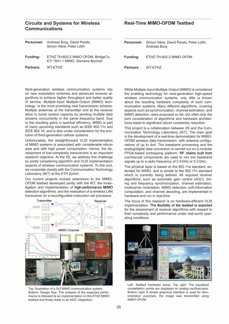
35
Circuits and Systems for Wireless Communications
Personnel: Simon Häne, David Perels, Peter Lüthi, Andreas Burg
Funding: ETHZ TH-602-2 MIMO OFDM
Partners: IKT-ETHZ
Real-Time MIMO-OFDM Testbed
Next-generation wireless communication systems rely on new modulation schemes and advanced receiver al-gorithms to achieve higher throughput and better quality of service. Multiple-Input Multiple-Output (MIMO) tech-nology is the most promising new transmission scheme. Multiple antennas at the transmitter and at the receiver allow to boost system capacity by sending multiple data streams concurrently in the same frequency band. Due to the resulting gains in spectral efficiency, MIMO is part of many upcoming standards such as IEEE 802.11n and IEEE 802.16, and is also under consideration for the evo-lution of third-generation cellular systems.
Unfortunately, the straightforward VLSI implementation of MIMO systems is associated with considerable silicon area and with high power consumption. Hence, the de-velopment of low-complexity transceivers is an important research objective. At the IIS, we address this challenge by jointly considering algorithm and VLSI implementation aspects of wireless communication systems. To this end, we cooperate closely with the Communication Technology Laboratory (IKT) at the ETH Zurich.
Our current projects include extensions to the MIMO-OFDM testbed developed jointly with the IKT, the inves-tigation and implementation of high-performance MIMOhigh-performance MIMOMIMO detection algorithms, and the realization of a wireless LAN transceiver on a reconfigurable instruction set processor.
Top: Illustration of a 3x3 MIMO communication system. Bottom: Design flow: The analysis of the expected perfor-mance is followed by an implementation on the ETHZ MIMO testbed and finally leads to an ASIC integration.
Personnel: Andreas Burg, David Perels, Simon Häne, Peter Lüthi
Funding: ETHZ TH-602-2 MIMO OFDM, BridgeCo, KTI 7641.1 MIMO, Siemens Bocholt
Partners: IKT-ETHZ
While Multiple-Input Multiple-Output (MIMO) is considered the enabling technology for next-generation high-speed wireless communication systems, only little is known about the resulting hardware complexity of such com-munication systems. Many different algorithms, covering aspects such as synchronization, channel estimation, and MIMO detection, were proposed so far, but often only the joint consideration of algorithms and hardware architec-tures leads to significant silicon complexity reduction.
This project is a collaboration between IIS and the Com-munication Technology Laboratory (IKT). The main goal is the development of a real-time demonstrator for MIMO-OFDM wireless data transmission, with antenna configu-rations of up to 4x4. The baseband processing and the analog/digital data conversion is carried out on a modular FPGA-based prototyping platform. RF chains built fromRF chains built from commercial components are used to mix the baseband signals up to a radio frequency of 2.4 GHz or 5.2 GHz.
The physical layer is based on the 802.11a standard, ex-tended for MIMO, and is similar to the 802.11n standard which is currently being defined. All required receiver algorithms, such as automatic gain control (AGC), tim-ing and frequency synchronization, channel estimation, multicarrier modulation, MIMO detection, soft-information computation, and channel decoding, are implemented in hardware and run in real-time.
The focus of this research is on hardware-efficient VLSI implementation. The flexibility of the testbed is exploitedThe flexibility of the testbed is exploited for the assessment of receiver algorithms with respect to their complexity and performance under real-world oper-ating conditions.
Left: Testbed hardware setup. Top right: The equalized constellation points are displayed on analog oscilloscopes. Bottom right: A simple graphical interface is used for dem-onstration purposes, the image was transmitted using MIMO-OFDM .
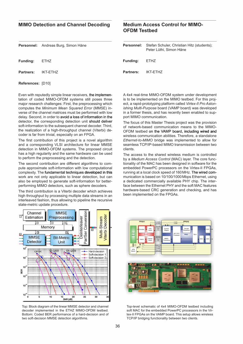
36
MIMO Detection and Channel Decoding Medium Access Control for MIMO-OFDM Testbed
Even with reputedly simple linear receivers, the implemen-the implemen-tation of coded MIMO-OFDM systems still poses three major research challenges: First, the preprocessing which computes the Minimum Mean Squared Error (MMSE) in-verse of the channel matrices must be performed with low delay. Second, in order to avoid a loss of information in theavoid a loss of information in the detector, the corresponding detection unit should delivershould deliver soft-information to the subsequent channel decoder. Third, the realization of a high-throughput channel (Viterbi) de-coder is far from trivial, especially on an FPGA.
The first contribution of this project is a novel algorithm and a corresponding VLSI architecture for linear MMSE detection in MIMO-OFDM systems. The proposed circuit has a high regularity and the same hardware can be used to perform the preprocessing and the detection.
The second contribution are different algorithms to com-pute approximate soft-information with low computational complexity. The fundamental techniques developed in thisfundamental techniques developed in thisdeveloped in this work are not only applicable to linear detection, but can also be employed to generate soft-information for better-performing MIMO detectors, such as sphere decoders.
The third contribution is a Viterbi decoder which achieves high throughput by processing multiple data streams in an interleaved fashion, thus allowing to pipeline the recursive state-metric update procedure.
Top: Block diagram of the linear MMSE detector and channel decoder implemented in the ETHZ MIMO-OFDM testbed. Bottom: Coded BER performance of a hard-decision and of two soft-decision MMSE detection algorithms.
Personnel: Andreas Burg, Simon Häne
Funding: ETHZ
Partners: IKT-ETHZ
References: [D10]
A 4x4 real-time MIMO-OFDM system under development is to be implemented on the MIMO testbed. For this proj-ect, a rapid-prototyping platform called Virtex-II Pro Aston-ishing Multi-Purpose board (VAMP board) was developed in a former thesis, and has recently been enabled to sup-port MIMO communication.
The focus of this Master Thesis project was the provision of network-based communication means to the MIMO-OFDM testbed on the VAMP board, including wired andon the VAMP board, including wired and, including wired and wireless communication abilities. Therefore, a standalone Ethernet-to-MIMO bridge was implemented to allow for seamless TCP/IP-based MIMO transmission between two clients.
The access to the shared wireless medium is controlled by a Medium Access Control (MAC) layer. The core func-tionality of the MAC has been designed in software for the embedded PowerPC processors on the Virtex-II FPGAs, running at a local clock speed of 160 MHz. The wired com-The wired com-munication is based on 10/100/1000 Mbps Ethernet, using a dedicated commercially available PHY chip. The inter-face between the Ethernet PHY and the soft MAC features hardware-based CRC generation and checking, and has been implemented on the FPGAs.
Top-level schematic of 4x4 MIMO-OFDM testbed including soft MAC for the embedded PowerPC processors in the Vir-tex-II FPGAs on the VAMP board. This setup allows wireless TCP/IP bridging functionality between two clients.
Personnel: Stefan Schuler, Christian Hitz (students); Peter Lüthi, Simon Häne
Funding: ETHZ
Partners: IKT-ETHZ
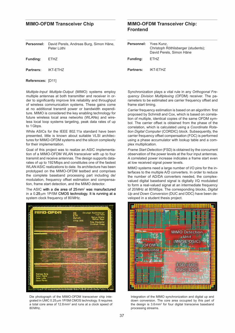
37
MIMO-OFDM Transceiver Chip MIMO-OFDM Transceiver Chip: Frontend
Multiple-Input Multiple-Output (MIMO) systems employ multiple antennas at both transmitter and receiver in or-der to significantly improve link reliability and throughput of wireless communication systems. These gains come at no additional transmit power or bandwidth expendi-ture. MIMO is considered the key enabling technology for future wireless local area networks (WLANs) and wire-less local loop systems targeting, peak data rates of up to 1 Gbps.
While ASICs for the IEEE 802.11a standard have been presented, little is known about suitable VLSI architec-tures for MIMO-OFDM systems and the silicon complexity for their implementation.
Goal of this project was to realize an ASIC implementa-tion of a MIMO-OFDM WLAN transceiver with up to four transmit and receive antennas. The design supports data-rates of up to 192 Mbps and constitutes one of the fastest WLAN ASIC realizations to date. Its architecture has been prototyped on the MIMO-OFDM testbed and comprises the complete baseband processing part including de/modulation, frequency offset estimation and compensa-tion, frame start detection, and the MIMO detector.
The ASIC with a die area of 25mmwith a die area of 25 mm2 was manufacturedwas manufactured in a 0.2525 mm 1P/5M CMOS technology. It is running at aCMOS technology. It is running at a system clock frequency of 80 MHz.
Die photograph of the MIMO-OFDM transceiver chip inte-grated in UMC 0.25 mm 1P/5M CMOS technology. It requires a total core area of 12.8 mm2 and runs at a clock speed of 80 MHz.
Personnel: David Perels, Andreas Burg, Simon Häne, Peter Lüthi
Funding: ETHZ
Partners: IKT-ETHZ
References: [D11]
Synchronization plays a vital rule in any Orthogonal Fre-quency Division Multiplexing (OFDM) receiver. The pa-rameters to be estimated are carrier frequency offset and frame start timing.
Carrier frequency estimation is based on an algorithm first proposed by Schmidl and Cox, which is based on correla-tion of multiple, identical copies of the same OFDM sym-bol. The carrier offset is obtained from the phase of the correlation, which is calculated using a Coordinate Rota-tion Digital Computer (CORDIC) block. Subsequently, the carrier frequency offset compensation (FOC) is performed using a phase accumulator with lookup table and a com-plex multiplication.
Frame Start Detection (FSD) is obtained by the concurrent observation of the power levels at the four input antennas. A correlated power increase indicates a frame start even at low received signal power levels.
MIMO systems need a large number of I/O pins for the in-terfaces to the multiple A/D converters. In order to reduce the number of AD/DA converters needed, the complex-valued digital baseband signal is digitally I/Q modulated to form a real-valued signal at an intermediate frequency of 20 MHz at 80 MSps. The corresponding blocks, Digital Up and Down Conversion (DUC and DDC) have been de-veloped in a student thesis project.
Integration of the MIMO synchronization and digital up and down conversion. The core area occupied by this part of the design is 3.6 mm2 for four digital transceive baseband processing streams.
Personnel: Yves Kunz, Christoph Röthlisberger (students); David Perels, Simon Häne
Funding: ETHZ
Partners: IKT-ETHZ
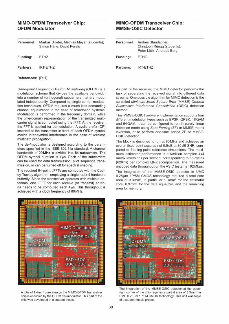
38
MIMO-OFDM Transceiver Chip: OFDM Modulator
MIMO-OFDM Transceiver Chip: MMSE-OSIC Detector
Orthogonal Frequency Division Multiplexing (OFDM) is a modulation scheme that divides the available bandwidth into a number of (orthogonal) subcarriers that are modu-lated independently. Compared to single-carrier modula-tion techniques, OFDM requires a much less demanding channel equalization in the case of broadband systems.Modulation is performed in the frequency domain, while the time-domain representation of the transmitted multi-carrier signal is computed using the IFFT. At the receiver, the FFT is applied for demodulation. A cyclic prefix (CP) inserted at the transmitter in front of each OFDM symbol avoids inter-symbol interference in the case of wireless multipath propagation.
The de-/modulator is designed according to the param-eters specified in the IEEE 802.11a standard. A channel bandwidth of 20MHz is divided into 64 subcarriers. The MHz is divided into 64 subcarriers. TheMHz is divided into 64 subcarriers. The OFDM symbol duration is 4 ms. Each of the subcarriers can be used for data transmission, pilot sequence trans-mission, or can be turned off for spectral shaping.
The required 64-point I/FFTs are computed with the Cool-ey-Tuckey algorithm, employing a single radix-4 hardware butterfly. Since the transceiver operates with multiple an-tennas, one I/FFT for each receive (or transmit) anten-na needs to be computed each 44 ms. This throughput is achieved with a clock frequency of 80 MHz.
A total of 1.4 mm2 core area on the MIMO-OFDM transceiver chip is occupied by the OFDM de-/modulator. This part of the chip was developed in a student thesis.
Personnel: Markus Billeter, Mathias Meyer (students); Simon Häne, David Perels
Funding: ETHZ
Partners: IKT-ETHZ
References: [D11]
As part of the receiver, the MIMO detector performs the task of separating the received signal into different data streams. One possible algorithm for MIMO detection is the so called Minimum Mean Square Error (MMSE) Ordered Successive Interference Cancellation (OSIC) detection method.
This MMSE-OSIC hardware implementation supports four different modulation types such as BPSK, QPSK, 16 QAM and 64 QAM. It can be configured to run in purely linear detection mode using Zero-Forcing (ZF) or MMSE matrix inversion, or to perform one-time sorted ZF or MMSE-OSIC detection.
The block is designed to run at 80 MHz and achieves an overall fixed-point accuracy of 0.5 dB at 30 dB SNR, com-pared to floating-point reference simulations. The maxi-mum estimator performance is 1.6 million complex 4x4 matrix inversions per second, corresponding to 65 cycles (620 ns) per complex QR-decomposition. The measured uncoded data throughput on the ASIC tester is 192 Mbps.
The integration of the MMSE-OSIC detector in UMC 0.25 mm 1P/5M CMOS technology required a total core area of 3.3 mm2, in particular 1.3 mm2 for the estimator core, 0.9 mm2 for the data equalizer, and the remaining area for memory.
The integration of the MMSE-OSIC detector at the upper right corner of the chip requires a partial area of 3.3 mm2 in UMC 0.25 mm 1P/5M CMOS technology. This unit was topic of a student thesis project
Personnel: Andres Staudacher, Christoph Rüegg (students); Peter Lüthi, Andreas Burg
Funding: ETHZ
Partners: IKT-ETHZ
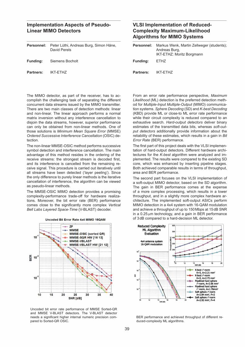
39
Implementation Aspects of Pseudo- Linear MIMO Detectors
VLSI Implementation of Reduced-Complexity Maximum-LikelihoodAlgorithms for MIMO Systems
The MIMO detector, as part of the receiver, has to ac-complish the challenging task of separating the different concurrent data streams issued by the MIMO transmitter. There are two main classes of detection methods: linear and non-linear. The linear approach performs a normal matrix inversion without any interference cancellation to disjoin the data streams, however, superior performance can only be obtained from non-linear methods. One of those solutions is Minimum Mean Square Error (MMSE) Ordered Successive Interference Cancellation (OSIC) de-tection.
The non-linear MMSE-OSIC method performs successive symbol detection and interference cancellation. The main advantage of this method resides in the ordering of the receive streams: the strongest stream is decoded first, and its interference is cancelled from the remaining re-ceive signal. This procedure is carried out iteratively until all streams have been detected (‘layer peeling’). Since the only difference to purely linear methods is the iterative cancellation of interference, the algorithm can be viewed as pseudo-linear methods.
The MMSE-OSIC MIMO detection provides a promising complexity-performance trade-off for hardware realiza-tions. Moreover, the bit error rate (BER) performance comes close to the significantly more complex Vertical Bell Labs Layered Space-Time (V-BLAST) decoder.
Uncoded bit error rate performance of MMSE Sorted-QR and MMSE V-BLAST detectors. The V-BLAST detector needs a significant higher internal numeric precision com-pared to Sorted-QR OSIC.
Personnel: Peter Lüthi, Andreas Burg, Simon Häne, David Perels
Funding: Siemens Bocholt
Partners: IKT-ETHZ
From an error rate performance perspective, Maximum Likelihood (ML) detection is the preferred detection meth-od for Multiple-Input Multiple-Output (MIMO) communica-tion systems. Sphere Decoding (SD) and K-best Decoding (KBD) provide ML or close-to ML error rate performance while their circuit complexity is reduced compared to an exhaustive search. Hard-output detectors deliver binary estimates of the transmitted data bits, whereas soft-out-put detectors additionally provide information about the reliability of these estimates, which results in a gain in Bit Error Rate (BER) performance.
The first part of this project deals with the VLSI implemen-tation of hard-output detectors. Different hardware archi-tectures for the K-best algorithm were analyzed and im-plemented. The results were compared to the existing SD core, which was enhanced by inserting pipeline stages. Both achieved comparable results in terms of throughput, area and BER performance.
The second part focuses on the VLSI implementation of a soft-output MIMO detector, based on the SD algorithm. The gain in BER performance comes at the expense of a more complex processing, which results in a lower throughput, and in a slightly more complex hardware ar-chitecture. The implemented soft-output ASICs perform MIMO detection in a 4x4 system with 16-QAM modulation and achieve a throughput of up to 150 Mbps at 15 dB SNR in a 0.25 mm technology, and a gain in BER performance of 3 dB compared to a hard-decision ML detector.
BER performance and achieved throughput of different re-duced-complexity ML algorithms.
Personnel: Markus Wenk, Martin Zellweger (students); Andreas Burg, IKT-ETHZ: Moritz Borgmann
Funding: ETHZ
Partners: IKT-ETHZ
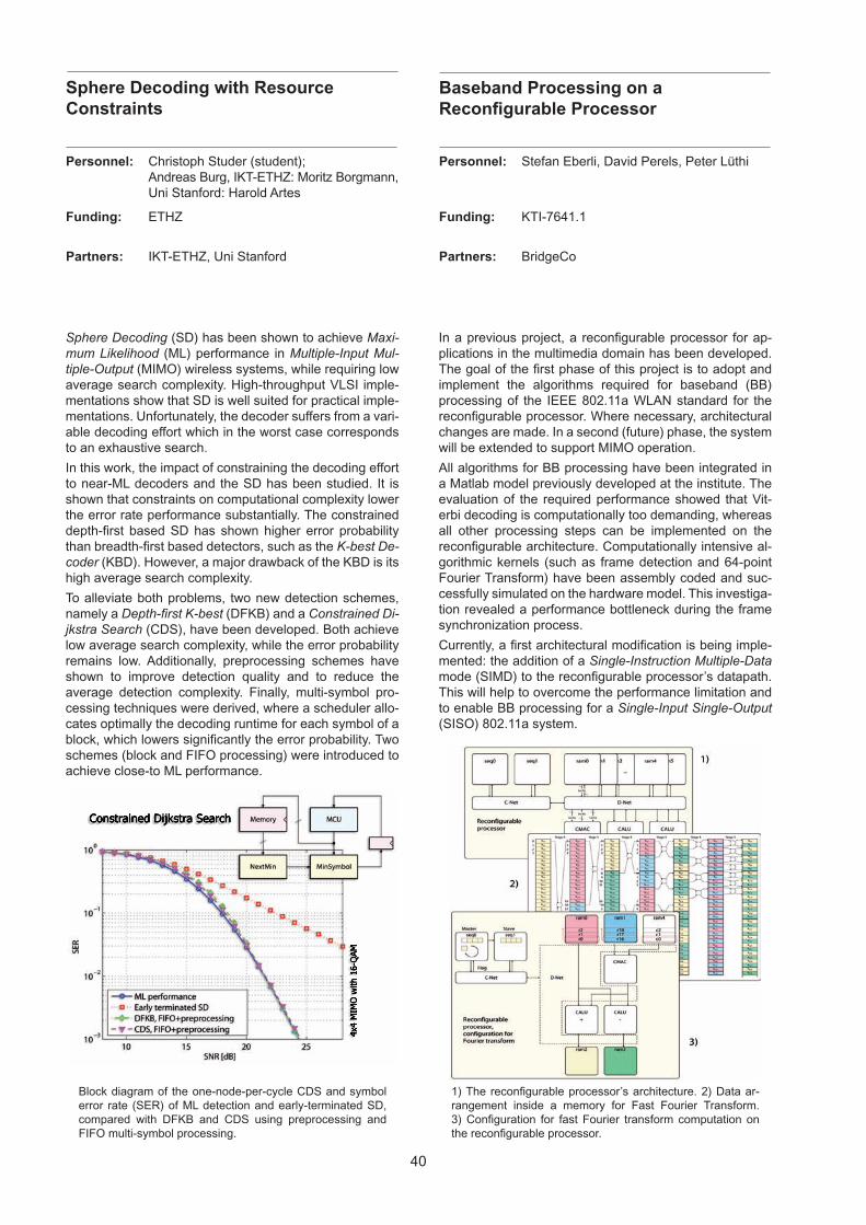
Sphere Decoding with Resource Constraints
Baseband Processing on a Reconfigurable Processor
Sphere Decoding (SD) has been shown to achieve Maxi-mum Likelihood (ML) performance in Multiple-Input Mul-tiple-Output (MIMO) wireless systems, while requiring low average search complexity. High-throughput VLSI imple-mentations show that SD is well suited for practical imple-mentations. Unfortunately, the decoder suffers from a vari-able decoding effort which in the worst case corresponds to an exhaustive search.
In this work, the impact of constraining the decoding effort to near-ML decoders and the SD has been studied. It is shown that constraints on computational complexity lower the error rate performance substantially. The constrained depth-first based SD has shown higher error probability than breadth-first based detectors, such as the K-best De-coder (KBD). However, a major drawback of the KBD is its high average search complexity.
To alleviate both problems, two new detection schemes, namely a Depth-first K-best (DFKB) and a Constrained Di-jkstra Search (CDS), have been developed. Both achieve low average search complexity, while the error probability remains low. Additionally, preprocessing schemes have shown to improve detection quality and to reduce the average detection complexity. Finally, multi-symbol pro-cessing techniques were derived, where a scheduler allo-cates optimally the decoding runtime for each symbol of a block, which lowers significantly the error probability. Two schemes (block and FIFO processing) were introduced to achieve close-to ML performance.
Block diagram of the one-node-per-cycle CDS and symbol error rate (SER) of ML detection and early-terminated SD, compared with DFKB and CDS using preprocessing and FIFO multi-symbol processing.
Personnel: Christoph Studer (student); Andreas Burg, IKT-ETHZ: Moritz Borgmann, Uni Stanford: Harold Artes
Funding: ETHZ
Partners: IKT-ETHZ, Uni Stanford
In a previous project, a reconfigurable processor for ap-plications in the multimedia domain has been developed. The goal of the first phase of this project is to adopt and implement the algorithms required for baseband (BB) processing of the IEEE 802.11a WLAN standard for the reconfigurable processor. Where necessary, architectural changes are made. In a second (future) phase, the system will be extended to support MIMO operation.
All algorithms for BB processing have been integrated in a Matlab model previously developed at the institute. The evaluation of the required performance showed that Vit-erbi decoding is computationally too demanding, whereas all other processing steps can be implemented on the reconfigurable architecture. Computationally intensive al-gorithmic kernels (such as frame detection and 64-point Fourier Transform) have been assembly coded and suc-cessfully simulated on the hardware model. This investiga-tion revealed a performance bottleneck during the frame synchronization process.
Currently, a first architectural modification is being imple-mented: the addition of a Single-Instruction Multiple-Data mode (SIMD) to the reconfigurable processor’s datapath. This will help to overcome the performance limitation and to enable BB processing for a Single-Input Single-Output (SISO) 802.11a system.
1) The reconfigurable processor’s architecture. 2) Data ar-rangement inside a memory for Fast Fourier Transform. 3) Configuration for fast Fourier transform computation on the reconfigurable processor.
Personnel: Stefan Eberli, David Perels, Peter Lüthi
Funding: KTI-7641.1
Partners: BridgeCo
40
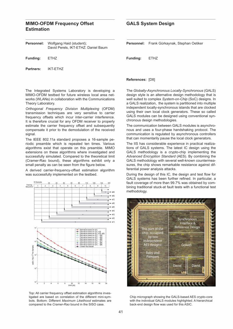
MIMO-OFDM Frequency Offset Estimation
GALS System Design
The Integrated Systems Laboratory is developing a MIMO-OFDM testbed for future wireless local area net-works (WLANs) in collaboration with the Communications Theory Laboratory.
Orthogonal Frequency Division Multiplexing (OFDM) transmission techniques are very sensitive to carrier frequency offsets which incur inter-carrier interference. It is therefore crucial for any OFDM receiver to properly estimate the carrier frequency offset and subsequently compensate it prior to the demodulation of the received signal.
The IEEE 802.11a standard proposes a 16-sample pe-riodic preamble which is repeated ten times. Various algorithms exist that operate on this preamble. MIMO extensions on these algorithms where investigated and successfully simulated. Compared to the theoretical limit (Cramer-Rao bound), these algorithms exhibit only a small penalty as can be seen from the figure below.
A derived carrier-frequency-offset estimation algorithm was successfully implemented on the testbed.
Top: All carrier frequency offset estimation algorithms inves-tigated are based on correlation of the different mini-sym-bols. Bottom: Different Maximum Likelihood estimates are compared to the Cramer-Rao bound in the SISO case.
Personnel: Wolfgang Haid (student); David Perels, IKT-ETHZ: Daniel Baum
Funding: ETHZ
Partners: IKT-ETHZ
The Globally-Asynchronous Locally-Synchronous (GALS) design style is an alternative design methodology that is well suited to complex System-on-Chip (SoC) designs. In a GALS realization, the system is partitioned into multiple independent locally-synchronous islands that are clocked using their own local clock generators. These so called GALS modules can be designed using conventional syn-chronous design methodologies.
The communication between GALS modules is asynchro-nous and uses a four-phase handshaking protocol. The communication is regulated by asynchronous controllers that can momentarily pause the local clock generators.
The IIS has considerable experience in practical realiza-tions of GALS systems. The latest IC design using the GALS methodology is a crypto-chip implementing the Advanced Encryption Standard (AES). By combining the GALS methodology with several well-known countermea-sures, the chip shows remarkable resistance against dif-ferential power analysis attacks.
During the design of this IC, the design and test flow for GALS systems has been further refined. In particular, a fault coverage of more than 99.7% was obtained by com-bining traditional stuck-at fault tests with a functional test methodology.
Chip micrograph showing the GALS-based AES crypto-core with the individual GALS modules highlighted. A hierarchical back-end design flow was used for this ASIC.
Personnel: Frank Gürkaynak, Stephan Oetiker
Funding: ETHZ
References: [D8]
41
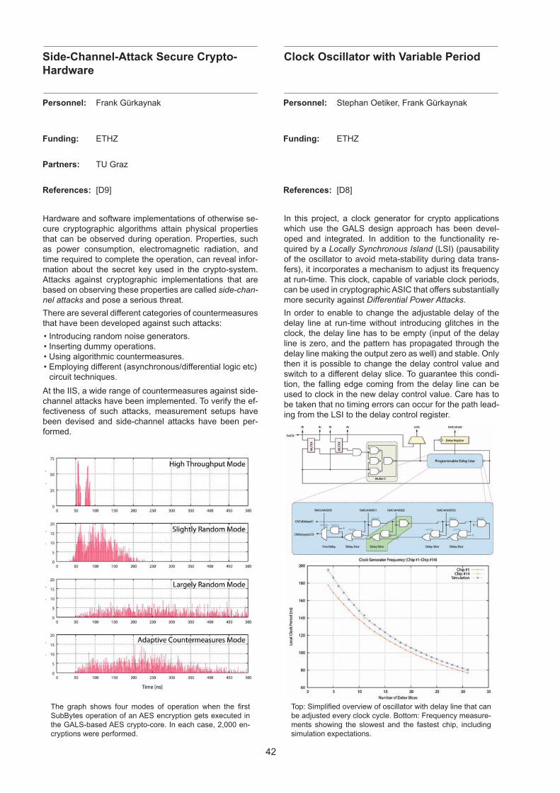
42
Side-Channel-Attack Secure Crypto-Hardware
Clock Oscillator with Variable Period
Hardware and software implementations of otherwise se-cure cryptographic algorithms attain physical properties that can be observed during operation. Properties, such as power consumption, electromagnetic radiation, and time required to complete the operation, can reveal infor-mation about the secret key used in the crypto-system. Attacks against cryptographic implementations that are based on observing these properties are called side-chan-nel attacks and pose a serious threat.
There are several different categories of countermeasures that have been developed against such attacks:
• Introducing random noise generators.• Inserting dummy operations.• Using algorithmic countermeasures.• Employing different (asynchronous/differential logic etc)
circuit techniques.
At the IIS, a wide range of countermeasures against side-channel attacks have been implemented. To verify the ef-fectiveness of such attacks, measurement setups have been devised and side-channel attacks have been per-formed.
The graph shows four modes of operation when the first SubBytes operation of an AES encryption gets executed in the GALS-based AES crypto-core. In each case, 2,000 en-cryptions were performed.
Personnel: Frank Gürkaynak
Funding: ETHZ
Partners: TU Graz
References: [D9]
Top: Simplified overview of oscillator with delay line that can be adjusted every clock cycle. Bottom: Frequency measure-ments showing the slowest and the fastest chip, including simulation expectations.
Personnel: Stephan Oetiker, Frank Gürkaynak
Funding: ETHZ
References: [D8]
In this project, a clock generator for crypto applications which use the GALS design approach has been devel-oped and integrated. In addition to the functionality re-quired by a Locally Synchronous Island (LSI) (pausability of the oscillator to avoid meta-stability during data trans-fers), it incorporates a mechanism to adjust its frequency at run-time. This clock, capable of variable clock periods, can be used in cryptographic ASIC that offers substantially more security against Differential Power Attacks.
In order to enable to change the adjustable delay of the delay line at run-time without introducing glitches in the clock, the delay line has to be empty (input of the delay line is zero, and the pattern has propagated through the delay line making the output zero as well) and stable. Only then it is possible to change the delay control value and switch to a different delay slice. To guarantee this condi-tion, the falling edge coming from the delay line can be used to clock in the new delay control value. Care has to be taken that no timing errors can occur for the path lead-ing from the LSI to the delay control register.
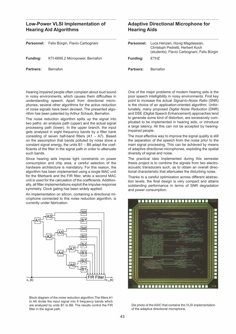
43
Low-Power VLSI Implementation of Hearing Aid Algorithms
Personnel: Luca Henzen, Hovig Magdassian, Christoph Pedretti, Herbert Koch (students); Flavio Carbognani, Felix Bürgin
Funding: ETHZ
Partners: Bernafon
Adaptive Directional Microphone for Hearing Aids
One of the major problems of modern hearing aids is the poor speech intelligibility in noisy environments. First key point to increase the actual Signal-to-Noise Ratio (SNR) is the choice of an application-oriented algorithm. Unfor-tunately, many proposed Digital Noise Reduction (DNR) and DSE (Digital Speech Enhancement) approaches tend to generate some kind of distortion, are excessively com-plicated to be implemented in hearing aids, or introduce a large latency. All this can not be accepted by hearing-impaired people.
The most effective way to improve the signal quality is still the separation of the speech from the noise prior to the main signal processing. This can be achieved by means of adaptive directional microphones, exploiting the spatial diversity of signal and noise.
The practical idea implemented during this semester thesis project is to combine the signals from two electro-acoustic transducers such, as to obtain an overall direc-tional characteristic that attenuates the disturbing noise.
Thanks to a careful optimization across different abstrac-tion levels, the final design is very compact and attains outstanding performance in terms of SNR degradation and power consumption.
Die photo of the ASIC that contains the VLSI implementation of the adaptive directional microphone.
Hearing impaired people often complain about loud sound in noisy environments, which causes them difficulties in understanding speech. Apart from directional micro-phones, several other algorithms for the active reduction of noise signals have been devised. The presented algo-rithm has been patented by Arthur Schaub, Bernafon.
The noise reduction algorithm splits up the signal into two paths: an analysis path (upper) and the actual signal processing path (lower). In the upper branch, the input gets analysed in eight frequency bands by a filter bank consisting of seven half-band filters (A1 – A7). Based on the assumption that bands polluted by noise show a constant signal energy, the units B1 – B8 adapt the coef-ficients of the filter in the signal path in order to attenuate such bands.
Since hearing aids impose tight constraints on power consumption and chip area, a careful selection of the hardware architecture is mandatory. For this reason, the algorithm has been implemented using a single MAC unit for the filterbank and the FIR filter, while a second MAC unit is used for the calculation of the coefficients. Addition-ally, all filter implementations exploit the impulse response symmetry. Clock gating has been widely applied.
An implementation on silicon, containing a directional mi-crophone connected to this noise reduction algorithm, is currently under fabrication.
Block diagram of the noise reduction algorithm.The filters A1 to A6 divide the input signal into 8 frequency bands which are analyzed by units B1 to B8. The results control the FIR filter in the signal path.
Personnel: Felix Bürgin, Flavio Carbognani
Funding: KTI-6695.2 Micropower, Bernafon
Partners: Bernafon
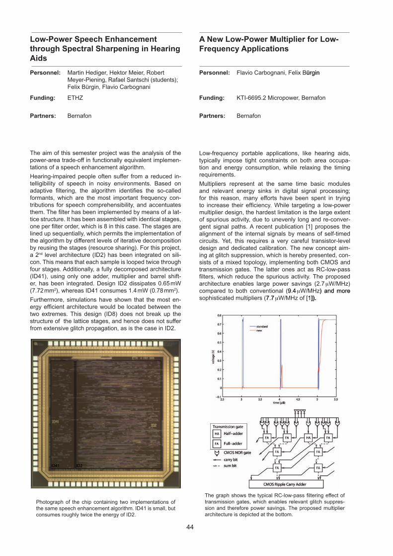
44
Personnel: Martin Hediger, Hektor Meier, Robert Meyer-Piening, Rafael Santschi (students); Felix Bürgin, Flavio Carbognani
Funding: ETHZ
Partners: Bernafon
Low-Power Speech Enhancement through Spectral Sharpening in Hearing Aids
A New Low-Power Multiplier for Low-Frequency Applications
Low-frequency portable applications, like hearing aids, typically impose tight constraints on both area occupa-tion and energy consumption, while relaxing the timing requirements.
Multipliers represent at the same time basic modules and relevant energy sinks in digital signal processing; for this reason, many efforts have been spent in trying to increase their efficiency. While targeting a low-power multiplier design, the hardest limitation is the large extent of spurious activity, due to unevenly long and re-conver-gent signal paths. A recent publication [1] proposes the alignment of the internal signals by means of self-timed circuits. Yet, this requires a very careful transistor-level design and dedicated calibration. The new concept aim-ing at glitch suppression, which is hereby presented, con-sists of a mixed topology, implementing both CMOS and transmission gates. The latter ones act as RC-low-pass filters, which reduce the spurious activity. The proposed architecture enables large power savings (2.7 mW/MHz) compared to both conventional (9.49.4 mW/MHz) and more) and more sophisticated multipliers (7.77.7 mW/MHz of [1]).1]).]).).
The graph shows the typical RC-low-pass filtering effect of transmission gates, which enables relevant glitch suppres-sion and therefore power savings. The proposed multiplier architecture is depicted at the bottom.
Personnel: Flavio Carbognani, Felix Bürginürgin
Funding: KTI-6695.2 Micropower, Bernafon
Partners: Bernafon
The aim of this semester project was the analysis of the power-area trade-off in functionally equivalent implemen-tations of a speech enhancement algorithm.
Hearing-impaired people often suffer from a reduced in-telligibility of speech in noisy environments. Based on adaptive filtering, the algorithm identifies the so-called formants, which are the most important frequency con-tributions for speech comprehensibility, and accentuates them. The filter has been implemented by means of a lat-tice structure. It has been assembled with identical stages, one per filter order, which is 8 in this case. The stages are lined up sequentially, which permits the implementation of the algorithm by different levels of iterative decomposition by reusing the stages (resource sharing). For this project, a 2nd level architecture (ID2) has been integrated on sili-con. This means that each sample is looped twice through four stages. Additionally, a fully decomposed architecture (ID41), using only one adder, multiplier and barrel shift-er, has been integrated. Design ID2 dissipates 0.65 mW (7.72 mm2), whereas ID41 consumes 1.4 mW (0.78 mm2).
Furthermore, simulations have shown that the most en-ergy efficient architecture would be located between the two extremes. This design (ID8) does not break up the structure of the lattice stages, and hence does not suffer from extensive glitch propagation, as is the case in ID2.
Photograph of the chip containing two implementations of the same speech enhancement algorithm. ID41 is small, but consumes roughly twice the energy of ID2.

45
Research Projects
Analog and Mixed-Signal Design
Coordinator:
Qiuting Huang
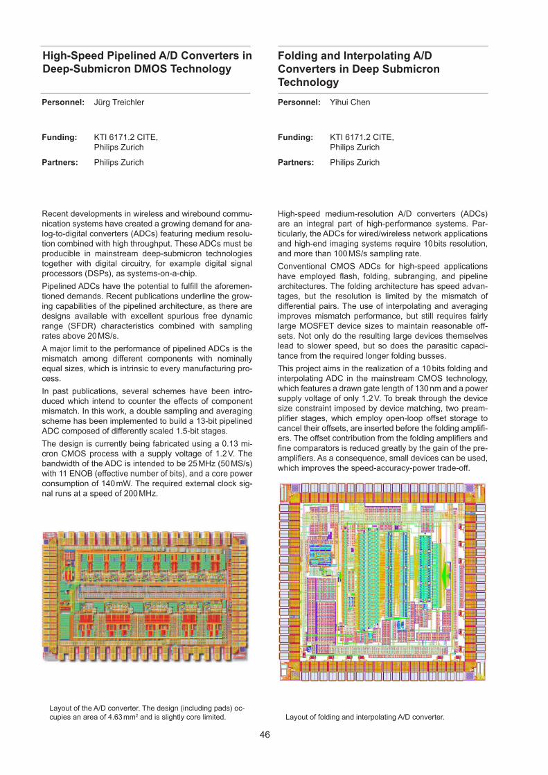
46
High-Speed Pipelined A/D Converters in Deep-Submicron DMOS Technology
Folding and Interpolating A/D Converters in Deep Submicron Technology
High-speed medium-resolution A/D converters (ADCs) are an integral part of high-performance systems. Par-ticularly, the ADCs for wired/wireless network applications and high-end imaging systems require 10 bits resolution, and more than 100 MS/s sampling rate.
Conventional CMOS ADCs for high-speed applications have employed flash, folding, subranging, and pipeline architectures. The folding architecture has speed advan-tages, but the resolution is limited by the mismatch of differential pairs. The use of interpolating and averaging improves mismatch performance, but still requires fairly large MOSFET device sizes to maintain reasonable off-sets. Not only do the resulting large devices themselves lead to slower speed, but so does the parasitic capaci-tance from the required longer folding busses.
This project aims in the realization of a 10 bits folding and interpolating ADC in the mainstream CMOS technology, which features a drawn gate length of 130 nm and a power supply voltage of only 1.2 V. To break through the device size constraint imposed by device matching, two pream-plifier stages, which employ open-loop offset storage to cancel their offsets, are inserted before the folding amplifi-ers. The offset contribution from the folding amplifiers and fine comparators is reduced greatly by the gain of the pre-amplifiers. As a consequence, small devices can be used, which improves the speed-accuracy-power trade-off.
Layout of folding and interpolating A/D converter.
Personnel: Yihui Chen
Funding: KTI 6171.2 CITE, Philips Zurich
Partners: Philips Zurich
Recent developments in wireless and wirebound commu-nication systems have created a growing demand for ana-log-to-digital converters (ADCs) featuring medium resolu-tion combined with high throughput. These ADCs must be producible in mainstream deep-submicron technologies together with digital circuitry, for example digital signal processors (DSPs), as systems-on-a-chip.
Pipelined ADCs have the potential to fulfill the aforemen-tioned demands. Recent publications underline the grow-ing capabilities of the pipelined architecture, as there are designs available with excellent spurious free dynamic range (SFDR) characteristics combined with sampling rates above 20 MS/s.
A major limit to the performance of pipelined ADCs is the mismatch among different components with nominally equal sizes, which is intrinsic to every manufacturing pro-cess.
In past publications, several schemes have been intro-duced which intend to counter the effects of component mismatch. In this work, a double sampling and averaging scheme has been implemented to build a 13-bit pipelined ADC composed of differently scaled 1.5-bit stages.
The design is currently being fabricated using a 0.13 mi-cron CMOS process with a supply voltage of 1.2 V. The bandwidth of the ADC is intended to be 25 MHz (50 MS/s) with 11 ENOB (effective number of bits), and a core power consumption of 140 mW. The required external clock sig-nal runs at a speed of 200 MHz.
Layout of the A/D converter. The design (including pads) oc-cupies an area of 4.63 mm2 and is slightly core limited.
Personnel: Jürg Treichler
Funding: KTI 6171.2 CITE, Philips Zurich
Partners: Philips Zurich
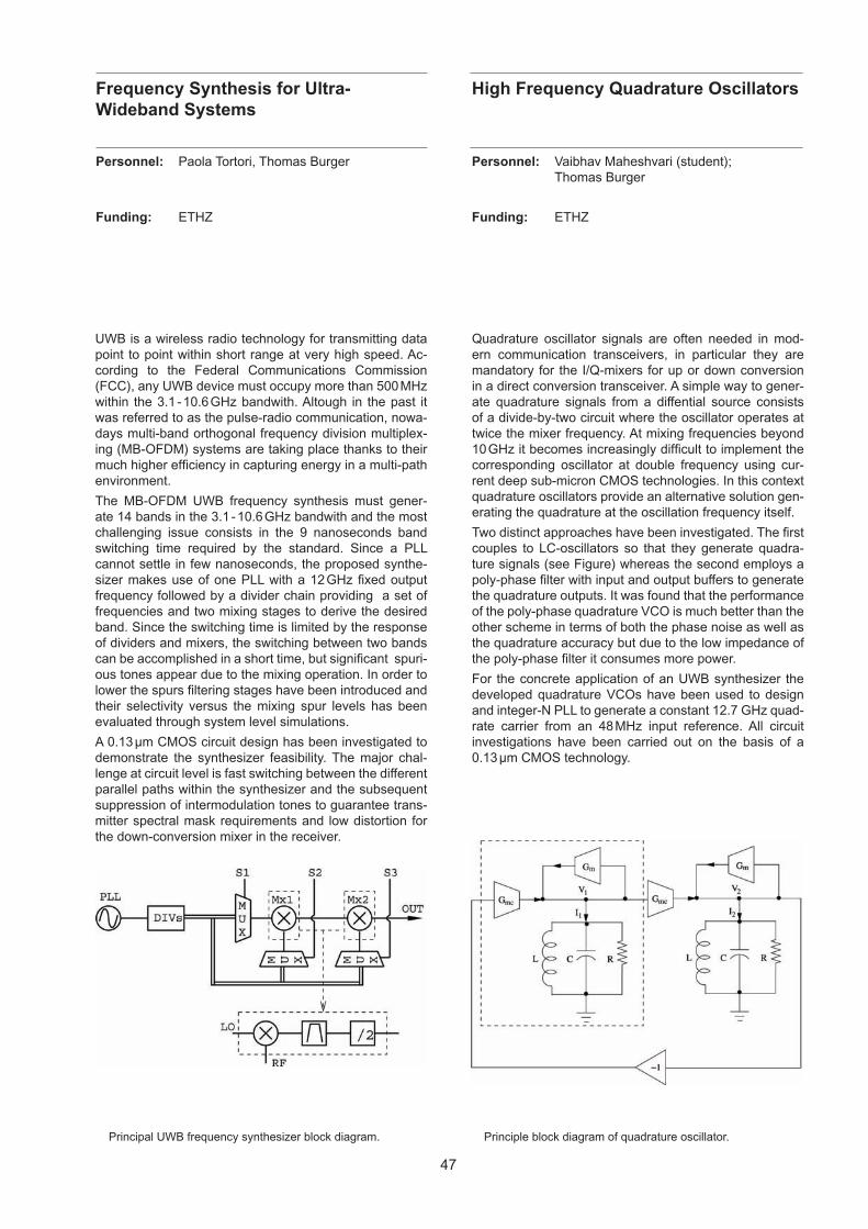
47
Personnel: Paola Tortori, Thomas Burger
Funding: ETHZ
Frequency Synthesis for Ultra-Wideband Systems
Personnel: Vaibhav Maheshvari (student); Thomas Burger
Funding: ETHZ
High Frequency Quadrature Oscillators
UWB is a wireless radio technology for transmitting data point to point within short range at very high speed. Ac-cording to the Federal Communications Commission (FCC), any UWB device must occupy more than 500 MHz within the 3.1 - 10.6 GHz bandwith. Altough in the past it was referred to as the pulse-radio communication, nowa-days multi-band orthogonal frequency division multiplex-ing (MB-OFDM) systems are taking place thanks to their much higher efficiency in capturing energy in a multi-path environment.
The MB-OFDM UWB frequency synthesis must gener-ate 14 bands in the 3.1 - 10.6 GHz bandwith and the most challenging issue consists in the 9 nanoseconds band switching time required by the standard. Since a PLL cannot settle in few nanoseconds, the proposed synthe-sizer makes use of one PLL with a 12 GHz fixed output frequency followed by a divider chain providing a set of frequencies and two mixing stages to derive the desired band. Since the switching time is limited by the response of dividers and mixers, the switching between two bands can be accomplished in a short time, but significant spuri-ous tones appear due to the mixing operation. In order to lower the spurs filtering stages have been introduced and their selectivity versus the mixing spur levels has been evaluated through system level simulations.
A 0.13 µm CMOS circuit design has been investigated to demonstrate the synthesizer feasibility. The major chal-lenge at circuit level is fast switching between the different parallel paths within the synthesizer and the subsequent suppression of intermodulation tones to guarantee trans-mitter spectral mask requirements and low distortion for the down-conversion mixer in the receiver.
Principal UWB frequency synthesizer block diagram.
Quadrature oscillator signals are often needed in mod-ern communication transceivers, in particular they are mandatory for the I/Q-mixers for up or down conversion in a direct conversion transceiver. A simple way to gener-ate quadrature signals from a diffential source consists of a divide-by-two circuit where the oscillator operates at twice the mixer frequency. At mixing frequencies beyond 10 GHz it becomes increasingly difficult to implement the corresponding oscillator at double frequency using cur-rent deep sub-micron CMOS technologies. In this context quadrature oscillators provide an alternative solution gen-erating the quadrature at the oscillation frequency itself.
Two distinct approaches have been investigated. The first couples to LC-oscillators so that they generate quadra-ture signals (see Figure) whereas the second employs a poly-phase filter with input and output buffers to generate the quadrature outputs. It was found that the performance of the poly-phase quadrature VCO is much better than the other scheme in terms of both the phase noise as well as the quadrature accuracy but due to the low impedance of the poly-phase filter it consumes more power.
For the concrete application of an UWB synthesizer the developed quadrature VCOs have been used to design and integer-N PLL to generate a constant 12.7 GHz quad-rate carrier from an 48 MHz input reference. All circuit investigations have been carried out on the basis of a 0.13 µm CMOS technology.
Principle block diagram of quadrature oscillator.
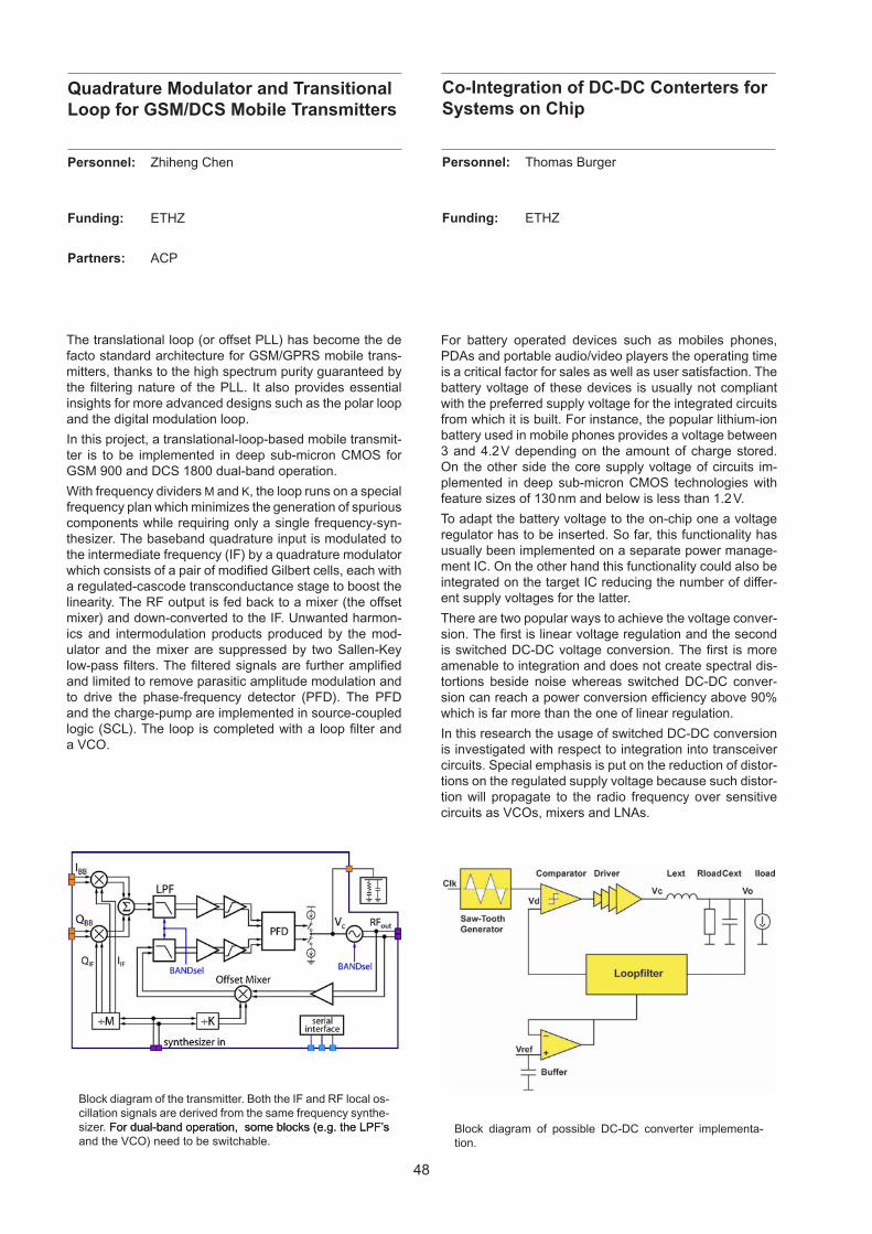
48
Quadrature Modulator and Transitional Loop for GSM/DCS Mobile Transmitters
Personnel: Thomas Burger
Funding: ETHZ
Co-Integration of DC-DC Conterters for Systems on Chip
The translational loop (or offset PLL) has become the de facto standard architecture for GSM/GPRS mobile trans-mitters, thanks to the high spectrum purity guaranteed by the filtering nature of the PLL. It also provides essential insights for more advanced designs such as the polar loop and the digital modulation loop.
In this project, a translational-loop-based mobile transmit-ter is to be implemented in deep sub-micron CMOS for GSM 900 and DCS 1800 dual-band operation.
With frequency dividers M and K, the loop runs on a special frequency plan which minimizes the generation of spurious components while requiring only a single frequency-syn-thesizer. The baseband quadrature input is modulated to the intermediate frequency (IF) by a quadrature modulator which consists of a pair of modified Gilbert cells, each with a regulated-cascode transconductance stage to boost the linearity. The RF output is fed back to a mixer (the offset mixer) and down-converted to the IF. Unwanted harmon-ics and intermodulation products produced by the mod-ulator and the mixer are suppressed by two Sallen-Key low-pass filters. The filtered signals are further amplified and limited to remove parasitic amplitude modulation and to drive the phase-frequency detector (PFD). The PFD and the charge-pump are implemented in source-coupled logic (SCL). The loop is completed with a loop filter and a VCO.
Block diagram of the transmitter. Both the IF and RF local os-cillation signals are derived from the same frequency synthe-sizer. For dual-band operation, some blocks (e.g. the LPF’sFor dual-band operation, some blocks (e.g. the LPF’s and the VCO) need to be switchable.
Personnel: Zhiheng Chen
Funding: ETHZ
Partners: ACP
For battery operated devices such as mobiles phones, PDAs and portable audio/video players the operating time is a critical factor for sales as well as user satisfaction. The battery voltage of these devices is usually not compliant with the preferred supply voltage for the integrated circuits from which it is built. For instance, the popular lithium-ion battery used in mobile phones provides a voltage between 3 and 4.2 V depending on the amount of charge stored. On the other side the core supply voltage of circuits im-plemented in deep sub-micron CMOS technologies with feature sizes of 130 nm and below is less than 1.2 V.
To adapt the battery voltage to the on-chip one a voltage regulator has to be inserted. So far, this functionality has usually been implemented on a separate power manage-ment IC. On the other hand this functionality could also be integrated on the target IC reducing the number of differ-ent supply voltages for the latter.
There are two popular ways to achieve the voltage conver-sion. The first is linear voltage regulation and the second is switched DC-DC voltage conversion. The first is more amenable to integration and does not create spectral dis-tortions beside noise whereas switched DC-DC conver-sion can reach a power conversion efficiency above 90% which is far more than the one of linear regulation.
In this research the usage of switched DC-DC conversion is investigated with respect to integration into transceiver circuits. Special emphasis is put on the reduction of distor-tions on the regulated supply voltage because such distor-tion will propagate to the radio frequency over sensitive circuits as VCOs, mixers and LNAs.
Block diagram of possible DC-DC converter implementa-tion.
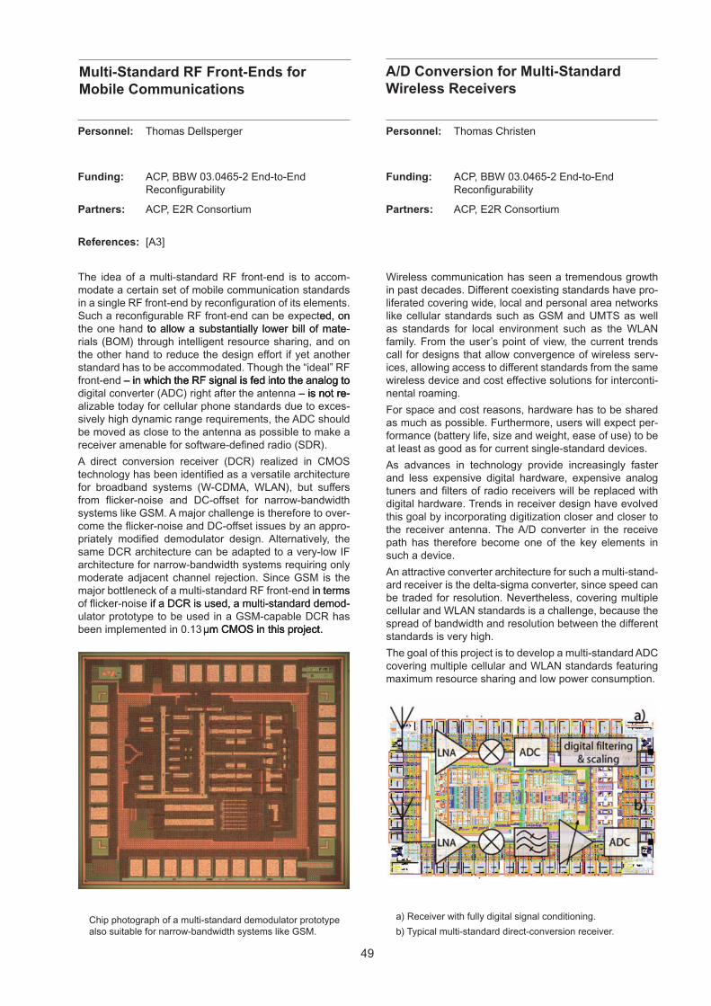
49
Multi-Standard RF Front-Ends for Mobile Communications
A/D Conversion for Multi-Standard Wireless Receivers
The idea of a multi-standard RF front-end is to accom-modate a certain set of mobile communication standards in a single RF front-end by reconfiguration of its elements. Such a reconfigurable RF front-end can be expected, oned, on the one hand to allow a substantially lower bill of mate-to allow a substantially lower bill of mate-rials (BOM) through intelligent resource sharing, and on the other hand to reduce the design effort if yet another standard has to be accommodated. Though the “ideal” RF front-end – in which the RF signal is fed into the analog to– in which the RF signal is fed into the analog to in which the RF signal is fed into the analog to digital converter (ADC) right after the antenna – is not re-– is not re- is not re-alizable today for cellular phone standards due to exces-sively high dynamic range requirements, the ADC should be moved as close to the antenna as possible to make a receiver amenable for software-defined radio (SDR).
A direct conversion receiver (DCR) realized in CMOS technology has been identified as a versatile architecture for broadband systems (W-CDMA, WLAN), but suffers from flicker-noise and DC-offset for narrow-bandwidth systems like GSM. A major challenge is therefore to over-come the flicker-noise and DC-offset issues by an appro-priately modified demodulator design. Alternatively, the same DCR architecture can be adapted to a very-low IF architecture for narrow-bandwidth systems requiring only moderate adjacent channel rejection. Since GSM is the major bottleneck of a multi-standard RF front-end in terms in terms of flicker-noise if a DCR is used, a multi-standard demod- if a DCR is used, a multi-standard demod-ulator prototype to be used in a GSM-capable DCR has been implemented in 0.13 µm CMOS in this project.µm CMOS in this project.m CMOS in this project.
Chip photograph of a multi-standard demodulator prototype also suitable for narrow-bandwidth systems like GSM.
Personnel: Thomas Dellsperger
Funding: ACP, BBW 03.0465-2 End-to-End Reconfigurability
Partners: ACP, E2R Consortium
References: [A3]
Wireless communication has seen a tremendous growth in past decades. Different coexisting standards have pro-liferated covering wide, local and personal area networks like cellular standards such as GSM and UMTS as well as standards for local environment such as the WLAN family. From the user’s point of view, the current trends call for designs that allow convergence of wireless serv-ices, allowing access to different standards from the same wireless device and cost effective solutions for interconti-nental roaming.
For space and cost reasons, hardware has to be shared as much as possible. Furthermore, users will expect per-formance (battery life, size and weight, ease of use) to be at least as good as for current single-standard devices.
As advances in technology provide increasingly faster and less expensive digital hardware, expensive analog tuners and filters of radio receivers will be replaced with digital hardware. Trends in receiver design have evolved this goal by incorporating digitization closer and closer to the receiver antenna. The A/D converter in the receive path has therefore become one of the key elements in such a device.
An attractive converter architecture for such a multi-stand-ard receiver is the delta-sigma converter, since speed can be traded for resolution. Nevertheless, covering multiple cellular and WLAN standards is a challenge, because the spread of bandwidth and resolution between the different standards is very high.
The goal of this project is to develop a multi-standard ADC covering multiple cellular and WLAN standards featuring maximum resource sharing and low power consumption.
a) Receiver with fully digital signal conditioning.
b) Typical multi-standard direct-conversion receiver.
Personnel: Thomas Christen
Funding: ACP, BBW 03.0465-2 End-to-End Reconfigurability
Partners: ACP, E2R Consortium
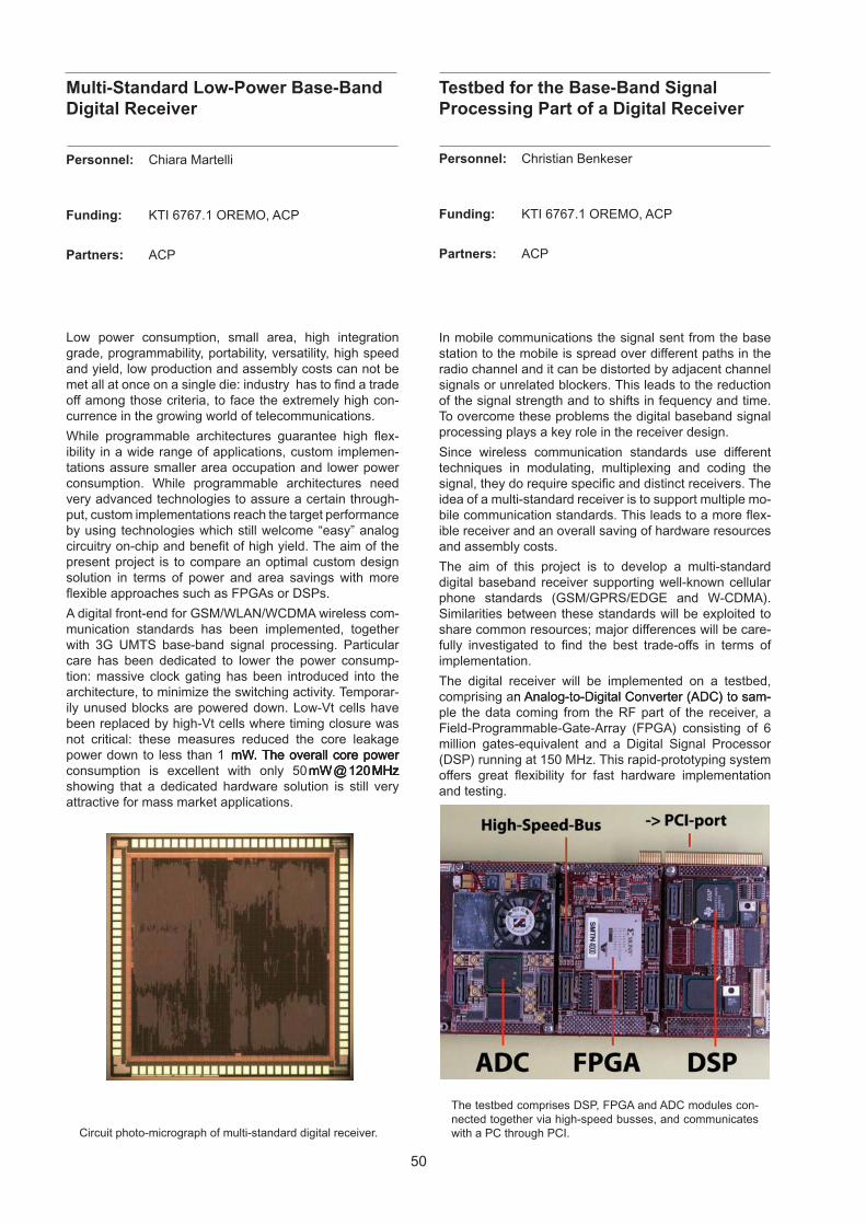
50
Multi-Standard Low-Power Base-Band Digital Receiver
Testbed for the Base-Band SignalProcessing Part of a Digital Receiver
Low power consumption, small area, high integration grade, programmability, portability, versatility, high speed and yield, low production and assembly costs can not be met all at once on a single die: industry has to find a trade off among those criteria, to face the extremely high con-currence in the growing world of telecommunications.
While programmable architectures guarantee high flex-ibility in a wide range of applications, custom implemen-tations assure smaller area occupation and lower power consumption. While programmable architectures need very advanced technologies to assure a certain through-put, custom implementations reach the target performance by using technologies which still welcome “easy” analog circuitry on-chip and benefit of high yield. The aim of the present project is to compare an optimal custom design solution in terms of power and area savings with more flexible approaches such as FPGAs or DSPs.
A digital front-end for GSM/WLAN/WCDMA wireless com-munication standards has been implemented, together with 3G UMTS base-band signal processing. Particular care has been dedicated to lower the power consump-tion: massive clock gating has been introduced into the architecture, to minimize the switching activity. Temporar-ily unused blocks are powered down. Low-Vt cells have been replaced by high-Vt cells where timing closure was not critical: these measures reduced the core leakage power down to less than 1 mW. The overall core power mW. The overall core powermW. The overall core power consumption is excellent with only 50mW@120MHz mW@120MHzmW @ 120MHz MHzMHz showing that a dedicated hardware solution is still very attractive for mass market applications.
Circuit photo-micrograph of multi-standard digital receiver.
Personnel: Chiara Martelli
Funding: KTI 6767.1 OREMO, ACP
Partners: ACP
In mobile communications the signal sent from the base station to the mobile is spread over different paths in the radio channel and it can be distorted by adjacent channel signals or unrelated blockers. This leads to the reduction of the signal strength and to shifts in fequency and time. To overcome these problems the digital baseband signal processing plays a key role in the receiver design.
Since wireless communication standards use different techniques in modulating, multiplexing and coding the signal, they do require specific and distinct receivers. The idea of a multi-standard receiver is to support multiple mo-bile communication standards. This leads to a more flex-ible receiver and an overall saving of hardware resources and assembly costs.
The aim of this project is to develop a multi-standard digital baseband receiver supporting well-known cellular phone standards (GSM/GPRS/EDGE and W-CDMA). Similarities between these standards will be exploited to share common resources; major differences will be care-fully investigated to find the best trade-offs in terms of implementation.
The digital receiver will be implemented on a testbed, comprising an Analog-to-Digital Converter (ADC) to sam-n Analog-to-Digital Converter (ADC) to sam-ple the data coming from the RF part of the receiver, a Field-Programmable-Gate-Array (FPGA) consisting of 6 million gates-equivalent and a Digital Signal Processor (DSP) running at 150 MHz. This rapid-prototyping system offers great flexibility for fast hardware implementation and testing.
The testbed comprises DSP, FPGA and ADC modules con-nected together via high-speed busses, and communicates with a PC through PCI.
Personnel: Christian Benkeser
Funding: KTI 6767.1 OREMO, ACP
Partners: ACP
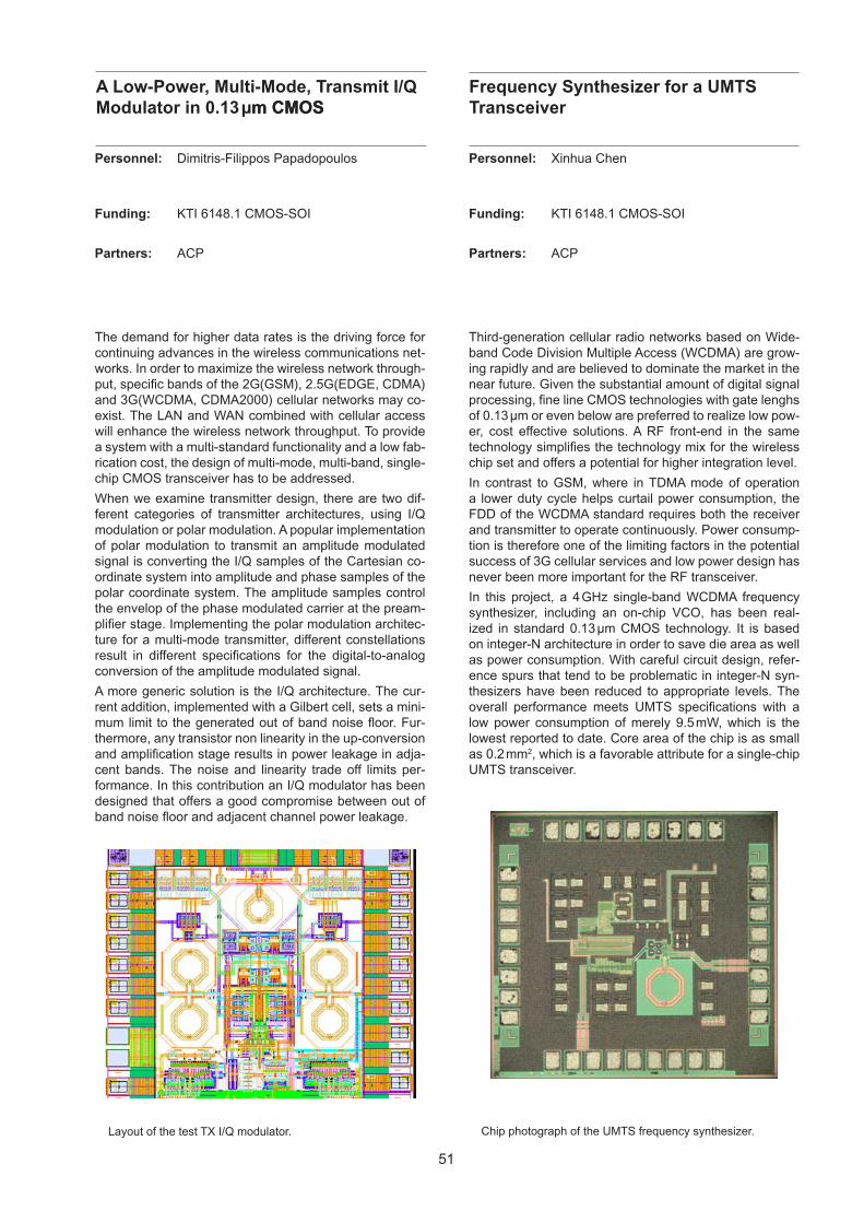
51
Personnel: Dimitris-Filippos Papadopoulos
Funding: KTI 6148.1 CMOS-SOI
Partners: ACP
A Low-Power, Multi-Mode, Transmit I/Q Modulator in 0.13 µm CMOSm CMOS
The demand for higher data rates is the driving force for continuing advances in the wireless communications net-works. In order to maximize the wireless network through-put, specific bands of the 2G(GSM), 2.5G(EDGE, CDMA) and 3G(WCDMA, CDMA2000) cellular networks may co-exist. The LAN and WAN combined with cellular access will enhance the wireless network throughput. To provide a system with a multi-standard functionality and a low fab-rication cost, the design of multi-mode, multi-band, single-chip CMOS transceiver has to be addressed.
When we examine transmitter design, there are two dif-ferent categories of transmitter architectures, using I/Q modulation or polar modulation. A popular implementation of polar modulation to transmit an amplitude modulated signal is converting the I/Q samples of the Cartesian co-ordinate system into amplitude and phase samples of the polar coordinate system. The amplitude samples control the envelop of the phase modulated carrier at the pream-plifier stage. Implementing the polar modulation architec-ture for a multi-mode transmitter, different constellations result in different specifications for the digital-to-analog conversion of the amplitude modulated signal.
A more generic solution is the I/Q architecture. The cur-rent addition, implemented with a Gilbert cell, sets a mini-mum limit to the generated out of band noise floor. Fur-thermore, any transistor non linearity in the up-conversion and amplification stage results in power leakage in adja-cent bands. The noise and linearity trade off limits per-formance. In this contribution an I/Q modulator has been designed that offers a good compromise between out of band noise floor and adjacent channel power leakage.
Layout of the test TX I/Q modulator.
Personnel: Xinhua Chen
Funding: KTI 6148.1 CMOS-SOI
Partners: ACP
Frequency Synthesizer for a UMTS Transceiver
Third-generation cellular radio networks based on Wide-band Code Division Multiple Access (WCDMA) are grow-ing rapidly and are believed to dominate the market in the near future. Given the substantial amount of digital signal processing, fine line CMOS technologies with gate lenghs of 0.13 µm or even below are preferred to realize low pow-er, cost effective solutions. A RF front-end in the same technology simplifies the technology mix for the wireless chip set and offers a potential for higher integration level.
In contrast to GSM, where in TDMA mode of operation a lower duty cycle helps curtail power consumption, the FDD of the WCDMA standard requires both the receiver and transmitter to operate continuously. Power consump-tion is therefore one of the limiting factors in the potential success of 3G cellular services and low power design has never been more important for the RF transceiver.
In this project, a 4 GHz single-band WCDMA frequency synthesizer, including an on-chip VCO, has been real-ized in standard 0.13 µm CMOS technology. It is based on integer-N architecture in order to save die area as well as power consumption. With careful circuit design, refer-ence spurs that tend to be problematic in integer-N syn-thesizers have been reduced to appropriate levels. The overall performance meets UMTS specifications with a low power consumption of merely 9.5 mW, which is the lowest reported to date. Core area of the chip is as small as 0.2 mm2, which is a favorable attribute for a single-chip UMTS transceiver.
Chip photograph of the UMTS frequency synthesizer.
52
Research Projects
Technology CAD
Coordinators:
Wolfgang Fichtner Andreas Schenk
Dölf Aemmer
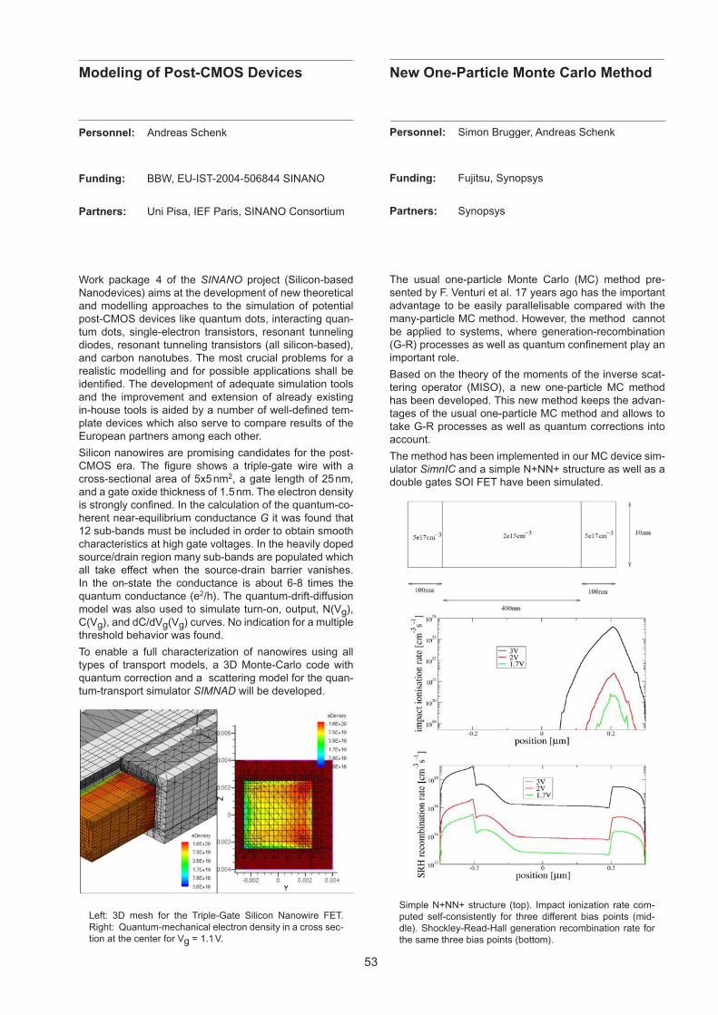
53
Personnel: Andreas Schenk
Funding: BBW, EU-IST-2004-506844 SINANO
Partners: Uni Pisa, IEF Paris, SINANO Consortium
Modeling of Post-CMOS Devices
Personnel: Simon Brugger, Andreas Schenk
Funding: Fujitsu, Synopsys
Partners: Synopsys
New One-Particle Monte Carlo Method
Work package 4 of the SINANO project (Silicon-based Nanodevices) aims at the development of new theoretical and modelling approaches to the simulation of potential post-CMOS devices like quantum dots, interacting quan-tum dots, single-electron transistors, resonant tunneling diodes, resonant tunneling transistors (all silicon-based), and carbon nanotubes. The most crucial problems for a realistic modelling and for possible applications shall be identified. The development of adequate simulation tools and the improvement and extension of already existing in-house tools is aided by a number of well-defined tem-plate devices which also serve to compare results of the European partners among each other.
Silicon nanowires are promising candidates for the post-CMOS era. The figure shows a triple-gate wire with a cross-sectional area of 5x5 nm2, a gate length of 25 nm, and a gate oxide thickness of 1.5 nm. The electron density is strongly confined. In the calculation of the quantum-co-herent near-equilibrium conductance G it was found that 12 sub-bands must be included in order to obtain smooth characteristics at high gate voltages. In the heavily doped source/drain region many sub-bands are populated which all take effect when the source-drain barrier vanishes. In the on-state the conductance is about 6-8 times the quantum conductance (e2/h). The quantum-drift-diffusion model was also used to simulate turn-on, output, N(Vg), C(Vg), and dC/dVg(Vg) curves. No indication for a multiple threshold behavior was found.
To enable a full characterization of nanowires using all types of transport models, a 3D Monte-Carlo code with quantum correction and a scattering model for the quan-tum-transport simulator SIMNAD will be developed.
Left: 3D mesh for the Triple-Gate Silicon Nanowire FET. Right: Quantum-mechanical electron density in a cross sec-tion at the center for Vg = 1.1 V.
The usual one-particle Monte Carlo (MC) method pre-sented by F. Venturi et al. 17 years ago has the important advantage to be easily parallelisable compared with the many-particle MC method. However, the method cannot be applied to systems, where generation-recombination (G-R) processes as well as quantum confinement play an important role.
Based on the theory of the moments of the inverse scat-tering operator (MISO), a new one-particle MC method has been developed. This new method keeps the advan-tages of the usual one-particle MC method and allows to take G-R processes as well as quantum corrections into account.
The method has been implemented in our MC device sim-ulator SimnIC and a simple N+NN+ structure as well as a double gates SOI FET have been simulated.
Simple N+NN+ structure (top). Impact ionization rate com-puted self-consistently for three different bias points (mid-dle). Shockley-Read-Hall generation recombination rate for the same three bias points (bottom).
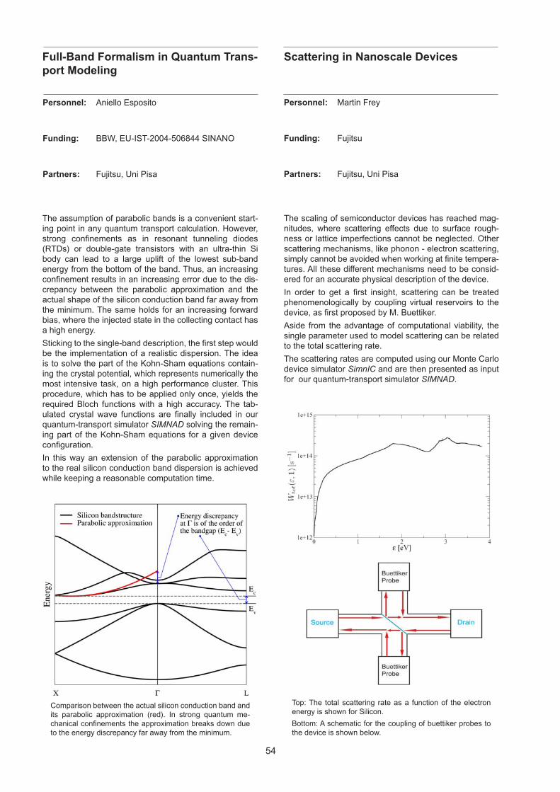
54
Full-Band Formalism in Quantum Trans-port Modeling
Scattering in Nanoscale Devices
The scaling of semiconductor devices has reached mag-nitudes, where scattering effects due to surface rough-ness or lattice imperfections cannot be neglected. Other scattering mechanisms, like phonon - electron scattering, simply cannot be avoided when working at finite tempera-tures. All these different mechanisms need to be consid-ered for an accurate physical description of the device.
In order to get a first insight, scattering can be treated phenomenologically by coupling virtual reservoirs to the device, as first proposed by M. Buettiker.
Aside from the advantage of computational viability, the single parameter used to model scattering can be related to the total scattering rate.
The scattering rates are computed using our Monte Carlo device simulator SimnIC and are then presented as input for our quantum-transport simulator SIMNAD.
Top: The total scattering rate as a function of the electron energy is shown for Silicon.
Bottom: A schematic for the coupling of buettiker probes to the device is shown below.
Personnel: Martin Frey
Funding: Fujitsu
Partners: Fujitsu, Uni Pisa
The assumption of parabolic bands is a convenient start-ing point in any quantum transport calculation. However, strong confinements as in resonant tunneling diodes (RTDs) or double-gate transistors with an ultra-thin Si body can lead to a large uplift of the lowest sub-band energy from the bottom of the band. Thus, an increasing confinement results in an increasing error due to the dis-crepancy between the parabolic approximation and the actual shape of the silicon conduction band far away from the minimum. The same holds for an increasing forward bias, where the injected state in the collecting contact has a high energy.
Sticking to the single-band description, the first step would be the implementation of a realistic dispersion. The idea is to solve the part of the Kohn-Sham equations contain-ing the crystal potential, which represents numerically the most intensive task, on a high performance cluster. This procedure, which has to be applied only once, yields the required Bloch functions with a high accuracy. The tab-ulated crystal wave functions are finally included in our quantum-transport simulator SIMNAD solving the remain-ing part of the Kohn-Sham equations for a given device configuration.
In this way an extension of the parabolic approximation to the real silicon conduction band dispersion is achieved while keeping a reasonable computation time.
Comparison between the actual silicon conduction band and its parabolic approximation (red). In strong quantum me-chanical confinements the approximation breaks down due to the energy discrepancy far away from the minimum.
Personnel: Aniello Esposito
Funding: BBW, EU-IST-2004-506844 SINANO
Partners: Fujitsu, Uni Pisa
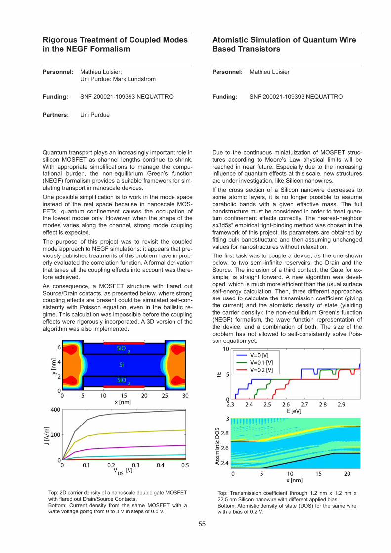
55
Personnel: Mathieu Luisier; Uni Purdue: Mark Lundstrom
Funding: SNF 200021-109393 NEQUATTRO
Partners: Uni Purdue
Rigorous Treatment of Coupled Modes in the NEGF Formalism
Personnel: Mathieu Luisier
Funding: SNF 200021-109393 NEQUATTRO
Atomistic Simulation of Quantum Wire Based Transistors
Quantum transport plays an increasingly important role in silicon MOSFET as channel lengths continue to shrink. With appropriate simplifications to manage the compu-tational burden, the non-equilibrium Green’s function (NEGF) formalism provides a suitable framework for sim-ulating transport in nanoscale devices.
One possible simplification is to work in the mode space instead of the real space because in nanoscale MOS-FETs, quantum confinement causes the occupation of the lowest modes only. However, when the shape of the modes varies along the channel, strong mode coupling effect is expected.
The purpose of this project was to revisit the coupled mode approach to NEGF simulations: it appears that pre-viously published treatments of this problem have improp-erly evaluated the correlation function. A formal derivation that takes all the coupling effects into account was there-fore achieved.
As consequence, a MOSFET structure with flared out Source/Drain contacts, as presented below, where strong coupling effects are present could be simulated self-con-sistently with Poisson equation, even in the ballistic re-gime. This calculation was impossible before the coupling effects were rigorously incorporated. A 3D version of the algorithm was also implemented.
Top: 2D carrier density of a nanoscale double gate MOSFET with flared out Drain/Source Contacts.Bottom: Current density from the same MOSFET with a Gate voltage going from 0 to 3 V in steps of 0.5 V.
Due to the continuous miniatuization of MOSFET struc-tures according to Moore’s Law physical limits will be reached in near future. Especially due to the increasing influence of quantum effects at this scale, new structures are under investigation, like Silicon nanowires.
If the cross section of a Silicon nanowire decreases to some atomic layers, it is no longer possible to assume parabolic bands with a given effective mass. The full bandstructure must be considered in order to treat quan-tum confinement effects correctly. The nearest-neighbor sp3d5s* empirical tight-binding method was chosen in the framework of this project. Its parameters are obtained by fitting bulk bandstructure and then assuming unchanged values for nanostructures without relaxation.
The first task was to couple a device, as the one shown below, to two semi-infinite reservoirs, the Drain and the Source. The inclusion of a third contact, the Gate for ex-ample, is straight forward. A new algorithm was devel-oped, which is much more efficient than the usual surface self-energy calculation. Then, three different approaches are used to calculate the transmission coefficient (giving the current) and the atomistic density of state (yielding the carrier density): the non-equilibrium Green’s function (NEGF) formalism, the wave function representation of the device, and a combination of both. The size of the problem has not allowed to self-consistently solve Pois-son equation yet.
Top: Transmission coefficient through 1.2 nm x 1.2 nm x 22.5 nm Silicon nanowire with different applied bias.Bottom: Atomistic density of state (DOS) for the same wire with a bias of 0.2 V.
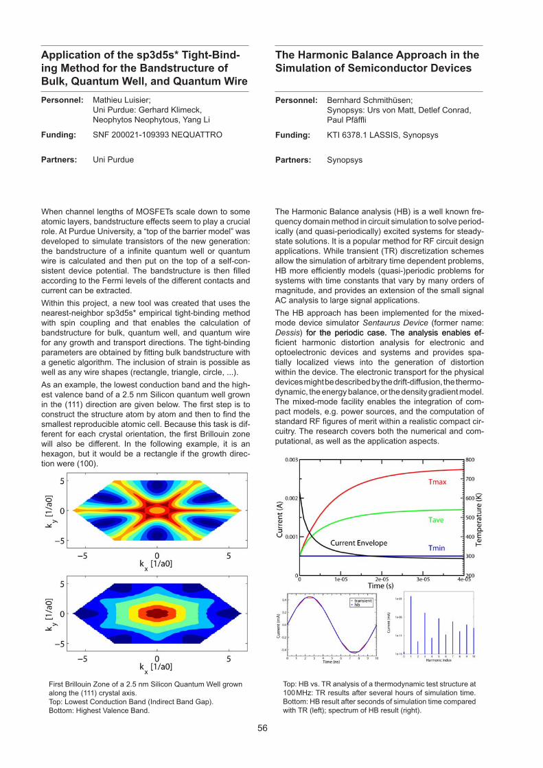
56
Personnel: Mathieu Luisier; Uni Purdue: Gerhard Klimeck, Neophytos Neophytous, Yang Li
Funding: SNF 200021-109393 NEQUATTRO
Partners: Uni Purdue
Application of the sp3d5s* Tight-Bind-ing Method for the Bandstructure of Bulk, Quantum Well, and Quantum Wire
The Harmonic Balance Approach in the Simulation of Semiconductor Devices
When channel lengths of MOSFETs scale down to some atomic layers, bandstructure effects seem to play a crucial role. At Purdue University, a “top of the barrier model” was developed to simulate transistors of the new generation: the bandstructure of a infinite quantum well or quantum wire is calculated and then put on the top of a self-con-sistent device potential. The bandstructure is then filled according to the Fermi levels of the different contacts and current can be extracted.
Within this project, a new tool was created that uses the nearest-neighbor sp3d5s* empirical tight-binding method with spin coupling and that enables the calculation of bandstructure for bulk, quantum well, and quantum wire for any growth and transport directions. The tight-binding parameters are obtained by fitting bulk bandstructure with a genetic algorithm. The inclusion of strain is possible as well as any wire shapes (rectangle, triangle, circle, ...).
As an example, the lowest conduction band and the high-est valence band of a 2.5 nm Silicon quantum well grown in the (111) direction are given below. The first step is to construct the structure atom by atom and then to find the smallest reproducible atomic cell. Because this task is dif-ferent for each crystal orientation, the first Brillouin zone will also be different. In the following example, it is an hexagon, but it would be a rectangle if the growth direc-tion were (100).
First Brillouin Zone of a 2.5 nm Silicon Quantum Well grown along the (111) crystal axis.Top: Lowest Conduction Band (Indirect Band Gap).Bottom: Highest Valence Band.
The Harmonic Balance analysis (HB) is a well known fre-quency domain method in circuit simulation to solve period-ically (and quasi-periodically) excited systems for steady-state solutions. It is a popular method for RF circuit design applications. While transient (TR) discretization schemes allow the simulation of arbitrary time dependent problems, HB more efficiently models (quasi-)periodic problems for systems with time constants that vary by many orders of magnitude, and provides an extension of the small signal AC analysis to large signal applications.
The HB approach has been implemented for the mixed-mode device simulator Sentaurus Device (former name: Dessis) for the periodic case. The analysis enables ef- for the periodic case. The analysis enables ef-ficient harmonic distortion analysis for electronic and optoelectronic devices and systems and provides spa-tially localized views into the generation of distortion within the device. The electronic transport for the physical devices might be described by the drift-diffusion, the thermo-dynamic, the energy balance, or the density gradient model. The mixed-mode facility enables the integration of com-pact models, e.g. power sources, and the computation of standard RF figures of merit within a realistic compact cir-cuitry. The research covers both the numerical and com-putational, as well as the application aspects.
Top: HB vs. TR analysis of a thermodynamic test structure at 100 MHz: TR results after several hours of simulation time. Bottom: HB result after seconds of simulation time compared with TR (left); spectrum of HB result (right).
Personnel: Bernhard Schmithüsen; Synopsys: Urs von Matt, Detlef Conrad, Paul Pfäffli
Funding: KTI 6378.1 LASSIS, Synopsys
Partners: Synopsys
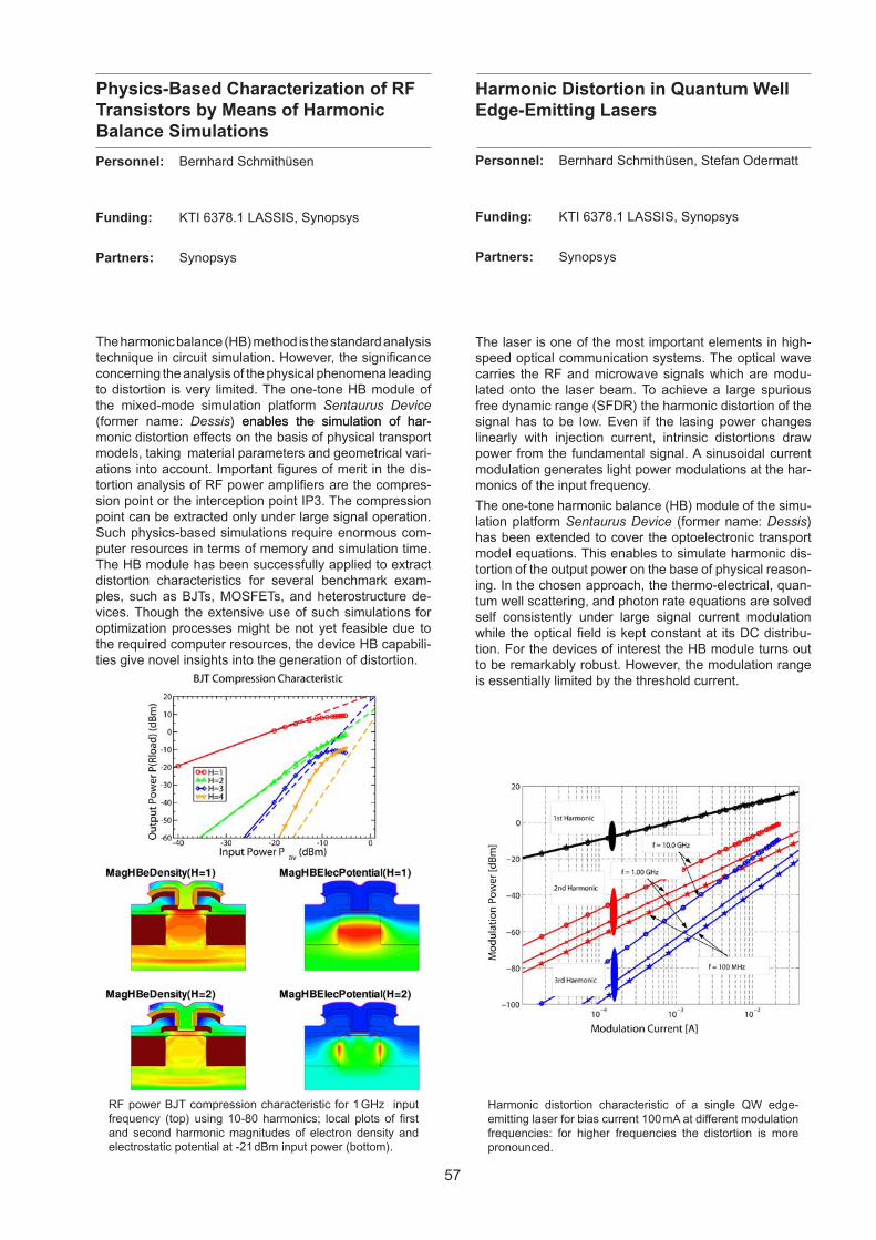
57
Physics-Based Characterization of RF Transistors by Means of Harmonic Balance Simulations
Harmonic Distortion in Quantum Well Edge-Emitting Lasers
The harmonic balance (HB) method is the standard analysis technique in circuit simulation. However, the significance concerning the analysis of the physical phenomena leading to distortion is very limited. The one-tone HB module of the mixed-mode simulation platform Sentaurus Device (former name: Dessis) enables the simulation of har- enables the simulation of har-monic distortion effects on the basis of physical transport models, taking material parameters and geometrical vari-ations into account. Important figures of merit in the dis-tortion analysis of RF power amplifiers are the compres-sion point or the interception point IP3. The compression point can be extracted only under large signal operation. Such physics-based simulations require enormous com-puter resources in terms of memory and simulation time. The HB module has been successfully applied to extract distortion characteristics for several benchmark exam-ples, such as BJTs, MOSFETs, and heterostructure de-vices. Though the extensive use of such simulations for optimization processes might be not yet feasible due to the required computer resources, the device HB capabili-ties give novel insights into the generation of distortion.
RF power BJT compression characteristic for 1 GHz input frequency (top) using 10-80 harmonics; local plots of first and second harmonic magnitudes of electron density and electrostatic potential at -21 dBm input power (bottom).
Personnel: Bernhard Schmithüsen
Funding: KTI 6378.1 LASSIS, Synopsys
Partners: Synopsys
The laser is one of the most important elements in high-speed optical communication systems. The optical wave carries the RF and microwave signals which are modu-lated onto the laser beam. To achieve a large spurious free dynamic range (SFDR) the harmonic distortion of the signal has to be low. Even if the lasing power changes linearly with injection current, intrinsic distortions draw power from the fundamental signal. A sinusoidal current modulation generates light power modulations at the har-monics of the input frequency.
The one-tone harmonic balance (HB) module of the simu-lation platform Sentaurus Device (former name: Dessis) has been extended to cover the optoelectronic transport model equations. This enables to simulate harmonic dis-tortion of the output power on the base of physical reason-ing. In the chosen approach, the thermo-electrical, quan-tum well scattering, and photon rate equations are solved self consistently under large signal current modulation while the optical field is kept constant at its DC distribu-tion. For the devices of interest the HB module turns out to be remarkably robust. However, the modulation range is essentially limited by the threshold current.
Harmonic distortion characteristic of a single QW edge-emitting laser for bias current 100 mA at different modulation frequencies: for higher frequencies the distortion is more pronounced.
Personnel: Bernhard Schmithüsen, Stefan Odermatt
Funding: KTI 6378.1 LASSIS, Synopsys
Partners: Synopsys
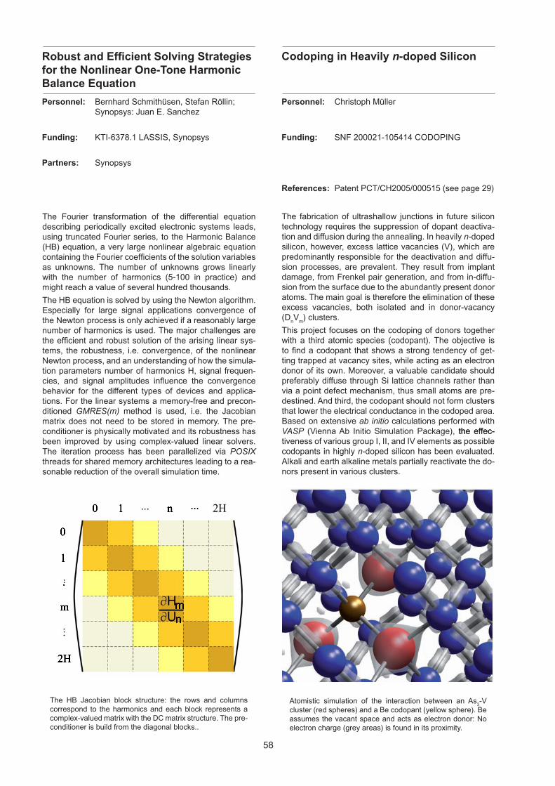
58
Personnel: Bernhard Schmithüsen, Stefan Röllin; Synopsys: Juan E. Sanchez
Funding: KTI-6378.1 LASSIS, Synopsys
Partners: Synopsys
Robust and Efficient Solving Strategies for the Nonlinear One-Tone Harmonic Balance Equation
Personnel: Christoph Müller
Funding: SNF 200021-105414 CODOPING
References: Patent PCT/CH2005/000515 (see page 29)
Codoping in Heavily n-doped Silicon
The fabrication of ultrashallow junctions in future silicon technology requires the suppression of dopant deactiva-tion and diffusion during the annealing. In heavily n-doped silicon, however, excess lattice vacancies (V), which are predominantly responsible for the deactivation and diffu-sion processes, are prevalent. They result from implant damage, from Frenkel pair generation, and from in-diffu-sion from the surface due to the abundantly present donor atoms. The main goal is therefore the elimination of these excess vacancies, both isolated and in donor-vacancy (D
nV
m) clusters.
This project focuses on the codoping of donors together with a third atomic species (codopant). The objective is to find a codopant that shows a strong tendency of get-ting trapped at vacancy sites, while acting as an electron donor of its own. Moreover, a valuable candidate should preferably diffuse through Si lattice channels rather than via a point defect mechanism, thus small atoms are pre-destined. And third, the codopant should not form clusters that lower the electrical conductance in the codoped area. Based on extensive ab initio calculations performed with VASP (Vienna Ab Initio Simulation Package), the effec-the effec-tiveness of various group I, II, and IV elements as possible codopants in highly n-doped silicon has been evaluated. Alkali and earth alkaline metals partially reactivate the do-nors present in various clusters.
Atomistic simulation of the interaction between an As3-V
cluster (red spheres) and a Be codopant (yellow sphere). Be assumes the vacant space and acts as electron donor: No electron charge (grey areas) is found in its proximity.
The Fourier transformation of the differential equation describing periodically excited electronic systems leads, using truncated Fourier series, to the Harmonic Balance (HB) equation, a very large nonlinear algebraic equation containing the Fourier coefficients of the solution variables as unknowns. The number of unknowns grows linearly with the number of harmonics (5-100 in practice) and might reach a value of several hundred thousands.
The HB equation is solved by using the Newton algorithm. Especially for large signal applications convergence of the Newton process is only achieved if a reasonably large number of harmonics is used. The major challenges are the efficient and robust solution of the arising linear sys-tems, the robustness, i.e. convergence, of the nonlinear Newton process, and an understanding of how the simula-tion parameters number of harmonics H, signal frequen-cies, and signal amplitudes influence the convergence behavior for the different types of devices and applica-tions. For the linear systems a memory-free and precon-ditioned GMRES(m) method is used, i.e. the Jacobian matrix does not need to be stored in memory. The pre-conditioner is physically motivated and its robustness has been improved by using complex-valued linear solvers. The iteration process has been parallelized via POSIX threads for shared memory architectures leading to a rea-sonable reduction of the overall simulation time.
The HB Jacobian block structure: the rows and columns correspond to the harmonics and each block represents a complex-valued matrix with the DC matrix structure. The pre-conditioner is build from the diagonal blocks..
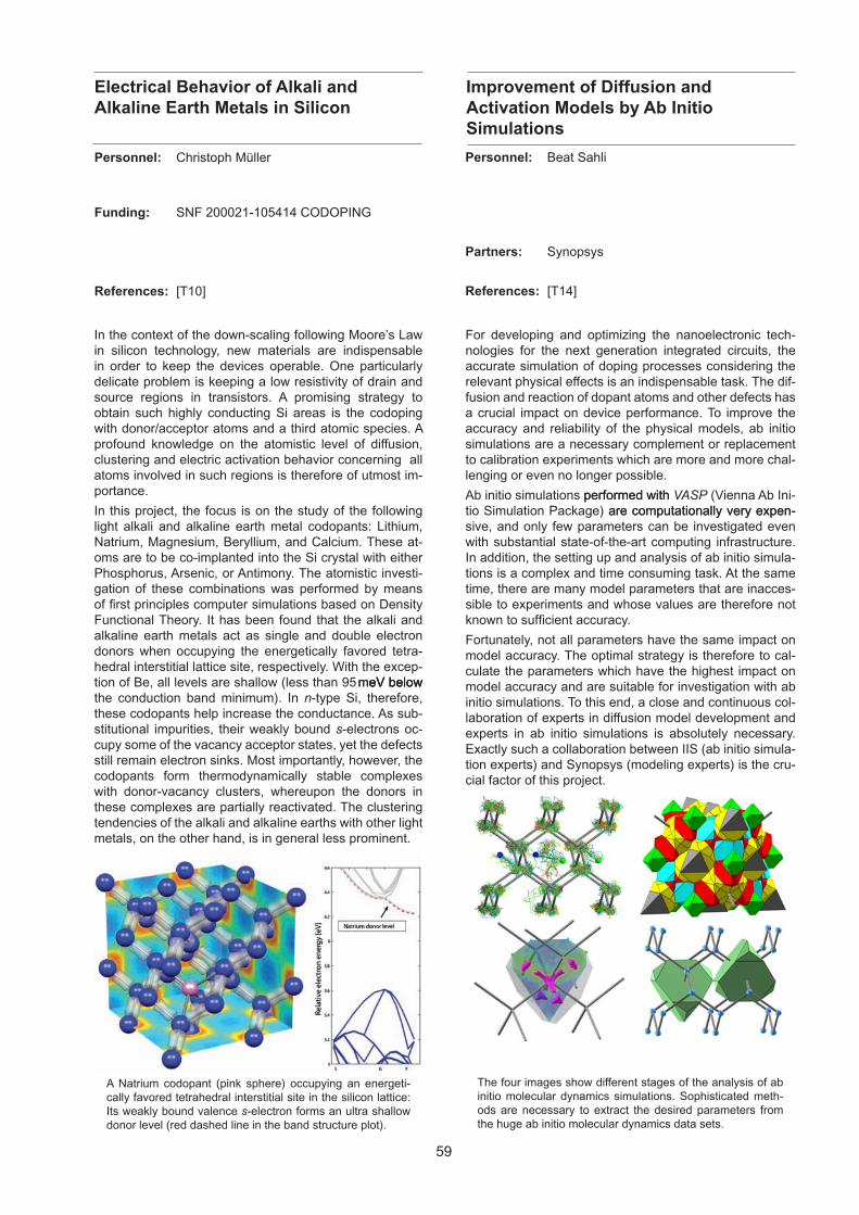
59
Personnel: Christoph Müller
Funding: SNF 200021-105414 CODOPING
References: [T10]
Electrical Behavior of Alkali and Alkaline Earth Metals in Silicon
Improvement of Diffusion and Activation Models by Ab Initio Simulations
In the context of the down-scaling following Moore’s Law in silicon technology, new materials are indispensable in order to keep the devices operable. One particularly delicate problem is keeping a low resistivity of drain and source regions in transistors. A promising strategy to obtain such highly conducting Si areas is the codoping with donor/acceptor atoms and a third atomic species. A profound knowledge on the atomistic level of diffusion, clustering and electric activation behavior concerning all atoms involved in such regions is therefore of utmost im-portance.
In this project, the focus is on the study of the following light alkali and alkaline earth metal codopants: Lithium, Natrium, Magnesium, Beryllium, and Calcium. These at-oms are to be co-implanted into the Si crystal with either Phosphorus, Arsenic, or Antimony. The atomistic investi-gation of these combinations was performed by means of first principles computer simulations based on Density Functional Theory. It has been found that the alkali and alkaline earth metals act as single and double electron donors when occupying the energetically favored tetra-hedral interstitial lattice site, respectively. With the excep-tion of Be, all levels are shallow (less than 95meV below meV beloweV below the conduction band minimum). In n-type Si, therefore, these codopants help increase the conductance. As sub-stitutional impurities, their weakly bound s-electrons oc-cupy some of the vacancy acceptor states, yet the defects still remain electron sinks. Most importantly, however, the codopants form thermodynamically stable complexes with donor-vacancy clusters, whereupon the donors in these complexes are partially reactivated. The clustering tendencies of the alkali and alkaline earths with other light metals, on the other hand, is in general less prominent.
A Natrium codopant (pink sphere) occupying an energeti-cally favored tetrahedral interstitial site in the silicon lattice: Its weakly bound valence s-electron forms an ultra shallow donor level (red dashed line in the band structure plot).
For developing and optimizing the nanoelectronic tech-nologies for the next generation integrated circuits, the accurate simulation of doping processes considering the relevant physical effects is an indispensable task. The dif-fusion and reaction of dopant atoms and other defects has a crucial impact on device performance. To improve the accuracy and reliability of the physical models, ab initio simulations are a necessary complement or replacement to calibration experiments which are more and more chal-lenging or even no longer possible.
Ab initio simulations performed withperformed with VASP (Vienna Ab Ini-tio Simulation Package) are computationally very expen-are computationally very expen-sive, and only few parameters can be investigated even with substantial state-of-the-art computing infrastructure. In addition, the setting up and analysis of ab initio simula-tions is a complex and time consuming task. At the same time, there are many model parameters that are inacces-sible to experiments and whose values are therefore not known to sufficient accuracy.
Fortunately, not all parameters have the same impact on model accuracy. The optimal strategy is therefore to cal-culate the parameters which have the highest impact on model accuracy and are suitable for investigation with ab initio simulations. To this end, a close and continuous col-laboration of experts in diffusion model development and experts in ab initio simulations is absolutely necessary. Exactly such a collaboration between IIS (ab initio simula-tion experts) and Synopsys (modeling experts) is the cru-cial factor of this project.
The four images show different stages of the analysis of ab initio molecular dynamics simulations. Sophisticated meth-ods are necessary to extract the desired parameters from the huge ab initio molecular dynamics data sets.
Personnel: Beat Sahli
Partners: Synopsys
References: [T14]
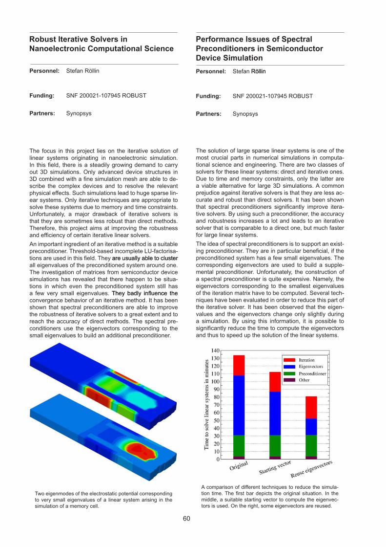
60
Robust Iterative Solvers in Nanoelectronic Computational Science
Performance Issues of Spectral Preconditioners in Semiconductor Device Simulation
The focus in this project lies on the iterative solution of linear systems originating in nanoelectronic simulation. In this field, there is a steadily growing demand to carry out 3D simulations. Only advanced device structures in 3D combined with a fine simulation mesh are able to de-scribe the complex devices and to resolve the relevant physical effects. Such simulations lead to huge sparse lin-ear systems. Only iterative techniques are appropriate to solve these systems due to memory and time constraints. Unfortunately, a major drawback of iterative solvers is that they are sometimes less robust than direct methods. Therefore, this project aims at improving the robustness and efficiency of certain iterative linear solvers.
An important ingredient of an iterative method is a suitable preconditioner. Threshold-based incomplete LU-factorisa-tions are used in this field. They are usually able to cluster are usually able to cluster all eigenvalues of the preconditioned system around one. The investigation of matrices from semiconductor device simulations has revealed that there happen to be situa-tions in which even the preconditioned system still has a few very small eigenvalues. They badly influence theThey badly influence the convergence behavior of an iterative method. It has been shown that spectral preconditioners are able to improve the robustness of iterative solvers to a great extent and to reach the accuracy of direct methods. The spectral pre-conditioners use the eigenvectors corresponding to the small eigenvalues to build an additional preconditioner.
Two eigenmodes of the electrostatic potential corresponding to very small eigenvalues of a linear system arising in the simulation of a memory cell.
Personnel: Stefan Röllin
Funding: SNF 200021-107945 ROBUST
Partners: Synopsys
The solution of large sparse linear systems is one of the most crucial parts in numerical simulations in computa-tional science and engineering. There are two classes of solvers for these linear systems: direct and iterative ones. Due to time and memory constraints, only the latter are a viable alternative for large 3D simulations. A common prejudice against iterative solvers is that they are less ac-curate and robust than direct solvers. It has been shown that spectral preconditioners significantly improve itera-tive solvers. By using such a preconditioner, the accuracy and robustness increases a lot and leads to an iterative solver that is comparable to a direct one, but much faster for large linear systems.
The idea of spectral preconditioners is to support an exist-ing preconditioner. They are in particular beneficial, if the preconditioned system has a few small eigenvalues. The corresponding eigenvectors are used to build a supple-mental preconditioner. Unfortunately, the construction of a spectral preconditioner is quite expensive. Namely, the eigenvectors corresponding to the smallest eigenvalues of the iteration matrix have to be computed. Several tech-niques have been evaluated in order to reduce this part of the iterative solver. It has been observed that the eigen-values and the eigenvectors change only slightly during a simulation. By using this information, it is possible to significantly reduce the time to compute the eigenvectors and thus to speed up the solution of the linear systems.
A comparison of different techniques to reduce the simula-tion time. The first bar depicts the original situation. In the middle, a suitable starting vector to compute the eigenvec-tors is used. On the right, some eigenvectors are reused.
Personnel: Stefan RöllinRöllin
Funding: SNF 200021-107945 ROBUST
Partners: Synopsys

61
Research Projects
Computational Optoelectronics
Coordinator:
Bernd Witzigmann
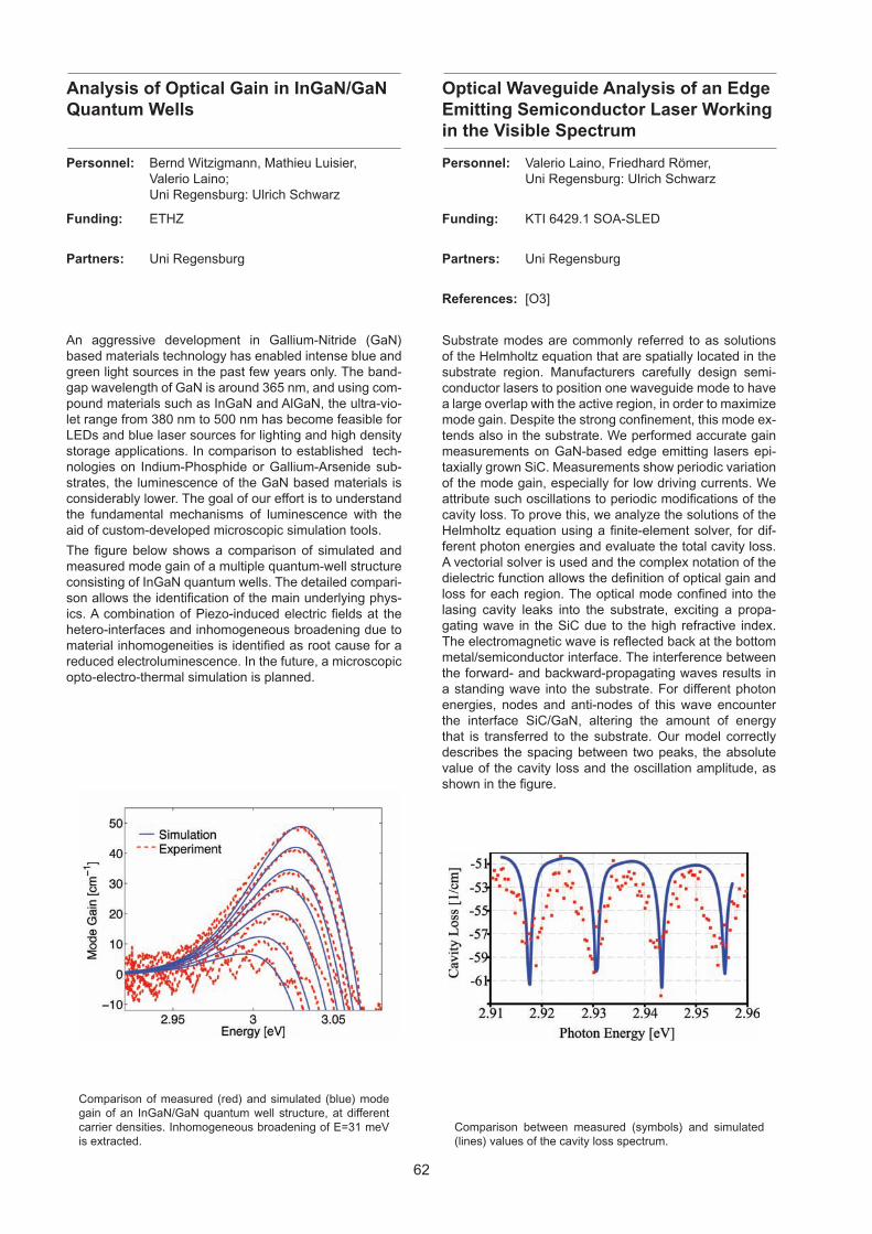
62
Analysis of Optical Gain in InGaN/GaN Quantum Wells
Optical Waveguide Analysis of an Edge Emitting Semiconductor Laser Working in the Visible Spectrum
Substrate modes are commonly referred to as solutions of the Helmholtz equation that are spatially located in the substrate region. Manufacturers carefully design semi-conductor lasers to position one waveguide mode to have a large overlap with the active region, in order to maximize mode gain. Despite the strong confinement, this mode ex-tends also in the substrate. We performed accurate gain measurements on GaN-based edge emitting lasers epi-taxially grown SiC. Measurements show periodic variation of the mode gain, especially for low driving currents. We attribute such oscillations to periodic modifications of the cavity loss. To prove this, we analyze the solutions of the Helmholtz equation using a finite-element solver, for dif-ferent photon energies and evaluate the total cavity loss. A vectorial solver is used and the complex notation of the dielectric function allows the definition of optical gain and loss for each region. The optical mode confined into the lasing cavity leaks into the substrate, exciting a propa-gating wave in the SiC due to the high refractive index. The electromagnetic wave is reflected back at the bottom metal/semiconductor interface. The interference between the forward- and backward-propagating waves results in a standing wave into the substrate. For different photon energies, nodes and anti-nodes of this wave encounter the interface SiC/GaN, altering the amount of energy that is transferred to the substrate. Our model correctly describes the spacing between two peaks, the absolute value of the cavity loss and the oscillation amplitude, as shown in the figure.
Comparison between measured (symbols) and simulated (lines) values of the cavity loss spectrum.
Personnel: Valerio Laino, Friedhard Römer, Uni Regensburg: Ulrich Schwarz
Funding: KTI 6429.1 SOA-SLED
Partners: Uni Regensburg
References: [O3]
Personnel: Bernd Witzigmann, Mathieu Luisier, Valerio Laino; Uni Regensburg: Ulrich Schwarz
Funding: ETHZ
Partners: Uni Regensburg
An aggressive development in Gallium-Nitride (GaN) based materials technology has enabled intense blue and green light sources in the past few years only. The band-gap wavelength of GaN is around 365 nm, and using com-pound materials such as InGaN and AlGaN, the ultra-vio-let range from 380 nm to 500 nm has become feasible for LEDs and blue laser sources for lighting and high density storage applications. In comparison to established tech-nologies on Indium-Phosphide or Gallium-Arsenide sub-strates, the luminescence of the GaN based materials is considerably lower. The goal of our effort is to understand the fundamental mechanisms of luminescence with the aid of custom-developed microscopic simulation tools.
The figure below shows a comparison of simulated and measured mode gain of a multiple quantum-well structure consisting of InGaN quantum wells. The detailed compari-son allows the identification of the main underlying phys-ics. A combination of Piezo-induced electric fields at the hetero-interfaces and inhomogeneous broadening due to material inhomogeneities is identified as root cause for a reduced electroluminescence. In the future, a microscopic opto-electro-thermal simulation is planned.
Comparison of measured (red) and simulated (blue) mode gain of an InGaN/GaN quantum well structure, at different carrier densities. Inhomogeneous broadening of E=31 meV is extracted.
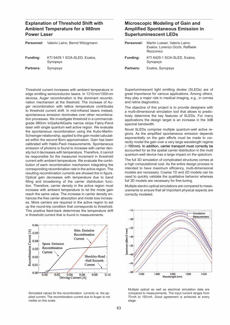
63
Personnel: Valerio Laino, Bernd Witzigmann
Funding: KTI 6429.1 SOA-SLED, Exalos, Synopsys
Partners: Synopsys
Explanation of Threshold Shift with Ambient Temperature for a 980nm Power Laser
Microscopic Modeling of Gain and Amplified Spontaneous Emission in Superluminescent LEDs
Superluminescent light emitting diodes (SLEDs) are of great importance for various applications. Among others, they play a major role in medical imaging, e.g., in cornea and retina diagnostics.
The objective of this project is to provide designers with a multi-dimensional simulation tool that allows to predic-tively determine the key features of SLEDs. For many applications the design target is an increase in the 3dB spectral bandwidth.
Novel SLEDs comprise multiple quantum-well active re-gions. As the amplified spontaneous emission depends exponentially on the gain efforts must be made to cor-rectly model the gain over a very large wavelength regime (~100nm). In addition, carrier transport must correctly be100 nm). In addition, carrier transport must correctly be accounted for as the spatial carrier distribution in the multi quantum-well device has a large impact on the spectrum.
The full 3D simulation of complicated structures comes at a high computational cost. As the entire design process is intended to have maximum efficiency, multi-dimensional models are necessary. Coarse 1D and 2D models can be used to quickly validate the qualitative behavior whereas full 3D models are necessary for fine-tuning.
Multiple electro-optical simulations are compared to meas-urements to ensure that all important physical aspects are correctly modeled.
Multiple optical as well as electrical simulation data are compared to measurements. The input current ranges from 70 mA to 150 mA. Good agreement is achieved at every stage.
Personnel: Martin Loeser, Valerio Laino; Exalos: Lorenzo Occhi, Raffaele Rezzonico
Funding: KTI 6429.1 SOA-SLED, Exalos, Synopsys
Partners: Exalos, Synopsys
Threshold current increases with ambient temperature in edge emitting semiconductor lasers. In 1310 nm/1550 nm devices, Auger recombination is the dominant recombi-nation mechanism at the theshold. The increase of Au-ger recombination with lattice temperature contributes to threshold current shift. In mid-infrared lasers instead, spontaneous emission dominates over other recombina-tion processes. We investigate threshold in a commercial-grade 980nm InGaAs/AlGaAs narrow stripe Fabry-Perot laser with single quantum well active region. We evaluate the spontaneous recombination using the Kubo-Martin-Schwinger relationship, applied to the gain model calculat-ed within the second Born approximation. Gain has been calibrated with Hakki-Paoli measurements. Spontaneous emission of photons is found to increase with carrier den-sity but it decreases with temperature. Therefore, it cannot be responsible for the measured increment in threshold current with ambient temperature. We evaluate the contri-bution of each recombination mechanism integrating the corresponding recombination rate in the active region. The resulting recombination currents are showed the in figure. Optical gain decreases with temperature due to band filling and broadening of the carrier distribution func-tion. Therefore, carrier density in the active region must increase with ambient temperature to let the mode gain reach the same value. The increase in carrier density en-hances the free carrier absorption and mode loss increas-es. More carriers are required in the active region to set up the round-trip condition that corresponds to threshold. This positive feed-back determines the temperature drift in threshold current that is found in measurements.
Simulated values for the recombination currents vs. the ap-plied current. The recombination current due to Auger is not visible on this scale.
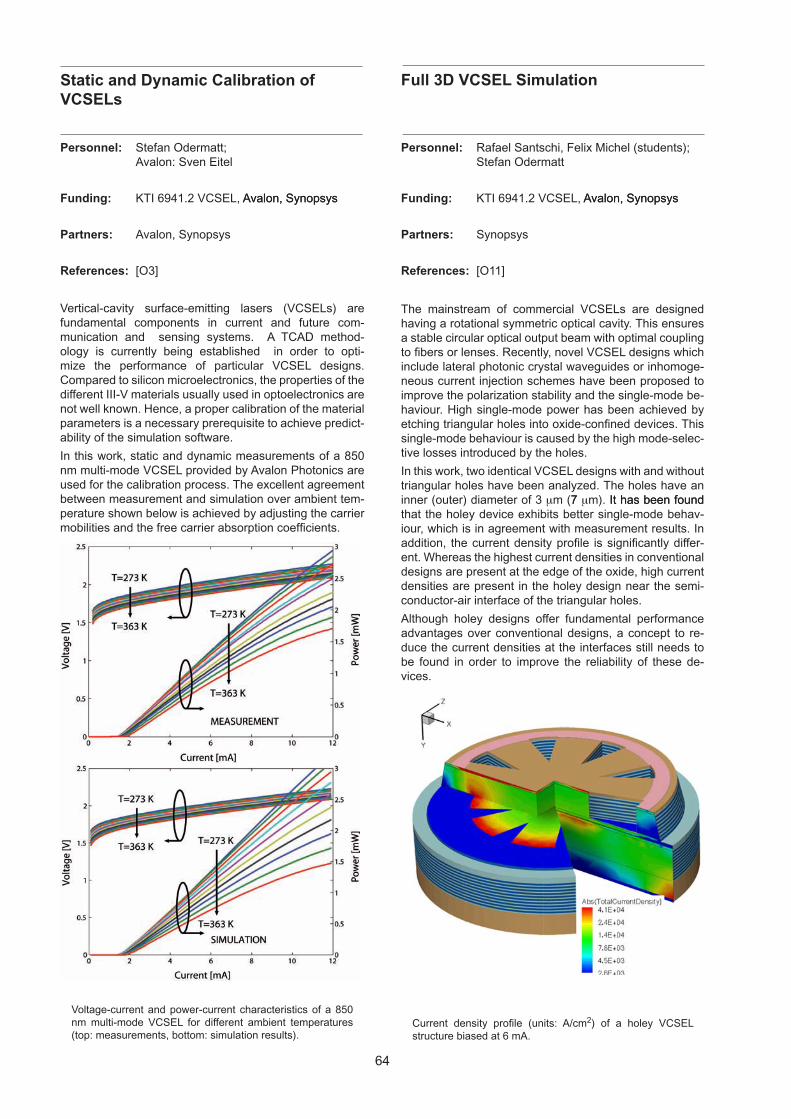
64
Personnel: Stefan Odermatt; Avalon: Sven Eitel
Funding: KTI 6941.2 VCSEL, Avalon, SynopsysAvalon, Synopsys
Partners: Avalon, Synopsys
References: [O3]
Static and Dynamic Calibration of VCSELs
Personnel: Rafael Santschi, Felix Michel (students); Stefan Odermatt
Funding: KTI 6941.2 VCSEL, Avalon, SynopsysAvalon, Synopsys
Partners: Synopsys
References: [O11]
Full 3D VCSEL Simulation
The mainstream of commercial VCSELs are designed having a rotational symmetric optical cavity. This ensures a stable circular optical output beam with optimal coupling to fibers or lenses. Recently, novel VCSEL designs which include lateral photonic crystal waveguides or inhomoge-neous current injection schemes have been proposed to improve the polarization stability and the single-mode be-haviour. High single-mode power has been achieved by etching triangular holes into oxide-confined devices. This single-mode behaviour is caused by the high mode-selec-tive losses introduced by the holes.
In this work, two identical VCSEL designs with and without triangular holes have been analyzed. The holes have an inner (outer) diameter of 3 mm (77 mm). It has been foundIt has been found that the holey device exhibits better single-mode behav-iour, which is in agreement with measurement results. In addition, the current density profile is significantly differ-ent. Whereas the highest current densities in conventional designs are present at the edge of the oxide, high current densities are present in the holey design near the semi-conductor-air interface of the triangular holes.
Although holey designs offer fundamental performance advantages over conventional designs, a concept to re-duce the current densities at the interfaces still needs to be found in order to improve the reliability of these de-vices.
Current density profile (units: A/cm2) of a holey VCSEL structure biased at 6 mA.
Vertical-cavity surface-emitting lasers (VCSELs) are fundamental components in current and future com-munication and sensing systems. A TCAD method-ology is currently being established in order to opti-mize the performance of particular VCSEL designs. Compared to silicon microelectronics, the properties of the different III-V materials usually used in optoelectronics are not well known. Hence, a proper calibration of the material parameters is a necessary prerequisite to achieve predict-ability of the simulation software.
In this work, static and dynamic measurements of a 850 nm multi-mode VCSEL provided by Avalon Photonics are used for the calibration process. The excellent agreement between measurement and simulation over ambient tem-perature shown below is achieved by adjusting the carrier mobilities and the free carrier absorption coefficients.
Voltage-current and power-current characteristics of a 850 nm multi-mode VCSEL for different ambient temperatures (top: measurements, bottom: simulation results).
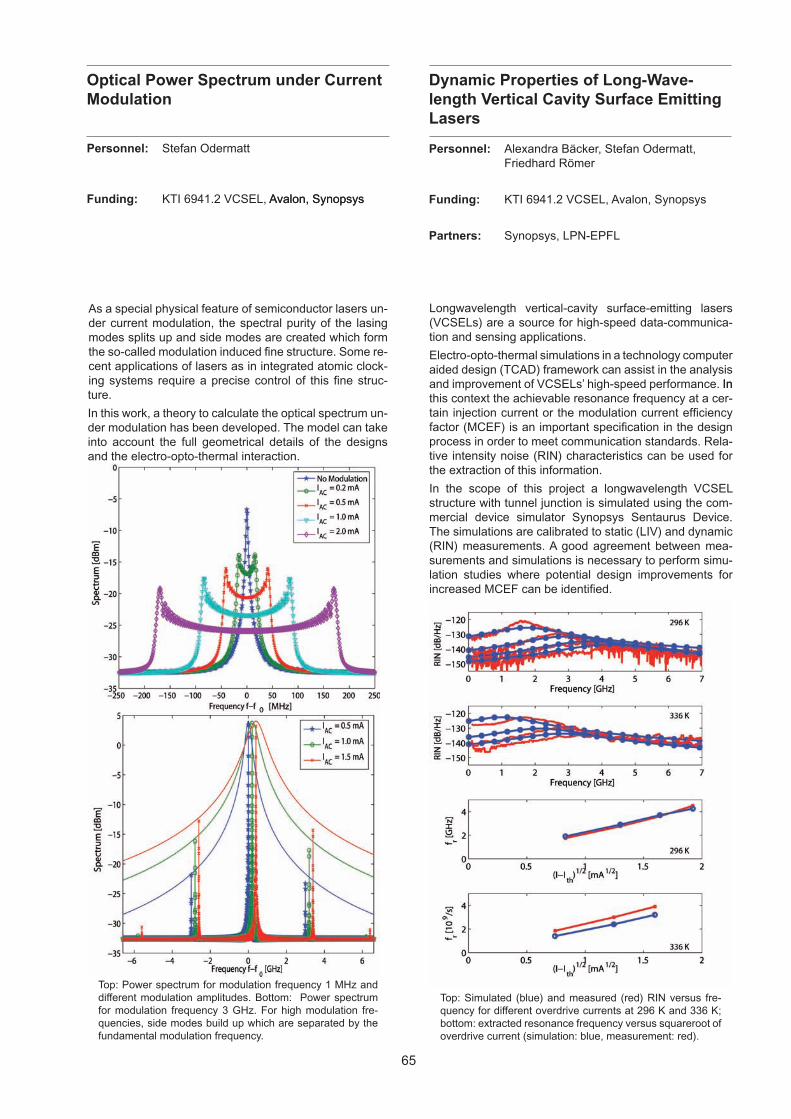
65
Personnel: Stefan Odermatt
Funding: KTI 6941.2 VCSEL, Avalon, SynopsysAvalon, Synopsys
Optical Power Spectrum under CurrentModulation
Dynamic Properties of Long-Wave-length Vertical Cavity Surface Emitting Lasers
Longwavelength vertical-cavity surface-emitting lasers (VCSELs) are a source for high-speed data-communica-tion and sensing applications.
Electro-opto-thermal simulations in a technology computer aided design (TCAD) framework can assist in the analysis and improvement of VCSELs’ high-speed performance. InIn this context the achievable resonance frequency at a cer-tain injection current or the modulation current efficiency factor (MCEF) is an important specification in the design process in order to meet communication standards. Rela-tive intensity noise (RIN) characteristics can be used for the extraction of this information.
In the scope of this project a longwavelength VCSEL structure with tunnel junction is simulated using the com-mercial device simulator Synopsys Sentaurus Device. The simulations are calibrated to static (LIV) and dynamic (RIN) measurements. A good agreement between mea-surements and simulations is necessary to perform simu-lation studies where potential design improvements for increased MCEF can be identified.
Top: Simulated (blue) and measured (red) RIN versus fre-quency for different overdrive currents at 296 K and 336 K; bottom: extracted resonance frequency versus squareroot of overdrive current (simulation: blue, measurement: red).
Personnel: Alexandra Bäcker, Stefan Odermatt, Friedhard Römer
Funding: KTI 6941.2 VCSEL, Avalon, Synopsys
Partners: Synopsys, LPN-EPFL
As a special physical feature of semiconductor lasers un-der current modulation, the spectral purity of the lasing modes splits up and side modes are created which form the so-called modulation induced fine structure. Some re-cent applications of lasers as in integrated atomic clock-ing systems require a precise control of this fine struc-ture.
In this work, a theory to calculate the optical spectrum un-der modulation has been developed. The model can take into account the full geometrical details of the designs and the electro-opto-thermal interaction.
Top: Power spectrum for modulation frequency 1 MHz and different modulation amplitudes. Bottom: Power spectrum for modulation frequency 3 GHz. For high modulation fre-quencies, side modes build up which are separated by the fundamental modulation frequency.
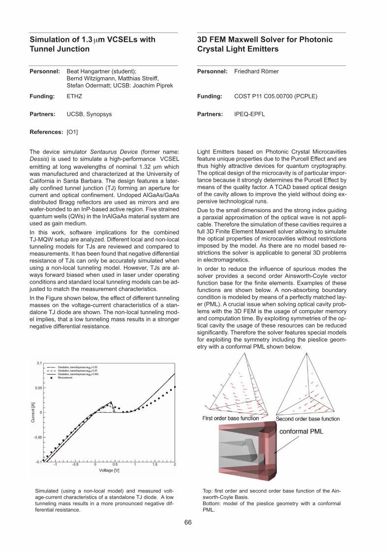
66
Personnel: Beat Hangartner (student); Bernd Witzigmann, Matthias Streiff, Stefan Odermatt; UCSB: Joachim Piprek
Funding: ETHZ
Partners: UCSB, Synopsys
References: [O1]
Simulation of 1.3 mm VCSELs with Tunnel Junction
3D FEM Maxwell Solver for Photonic Crystal Light Emitters
The device simulator Sentaurus Device (former name: Dessis) is used to simulate a high-performance VCSEL emitting at long wavelengths of nominal 1.32 mm which was manufactured and characterized at the University of California in Santa Barbara. The design features a later-ally confined tunnel junction (TJ) forming an aperture for current and optical confinement. Undoped AlGaAs/GaAs distributed Bragg reflectors are used as mirrors and are wafer-bonded to an InP-based active region. Five strained quantum wells (QWs) in the InAlGaAs material system are used as gain medium.
In this work, software implications for the combined TJ-MQW setup are analyzed. Different local and non-local tunneling models for TJs are reviewed and compared to measurements. It has been found that negative differential resistance of TJs can only be accurately simulated when using a non-local tunneling model. However, TJs are al-ways forward biased when used in laser under operating conditions and standard local tunneling models can be ad-justed to match the measurement characteristics.
In the Figure shown below, the effect of different tunneling masses on the voltage-current characteristics of a stan-dalone TJ diode are shown. The non-local tunneling mod-el implies, that a low tunneling mass results in a stronger negative differential resistance.
Simulated (using a non-local model) and measured volt-age-current characteristics of a standalone TJ diode. A low tunneling mass results in a more pronounced negative dif-ferential resistance.
Personnel: Friedhard Römer
Funding: COST P11 C05.00700 (PCPLE)
Partners: IPEQ-EPFL
Light Emitters based on Photonic Crystal Microcavities feature unique properties due to the Purcell Effect and are thus highly attractive devices for quantum cryptography. The optical design of the microcavity is of particular impor-tance because it strongly determines the Purcell Effect by means of the quality factor. A TCAD based optical design of the cavity allows to improve the yield without doing ex-pensive technological runs.
Due to the small dimensions and the strong index guiding a paraxial approximation of the optical wave is not appli-cable. Therefore the simulation of these cavities requires a full 3D Finite Element Maxwell solver allowing to simulate the optical properties of microcavities without restrictions imposed by the model. As there are no model based re-strictions the solver is applicable to general 3D problems in electromagnetics.
In order to reduce the influence of spurious modes the solver provides a second order Ainsworth-Coyle vector function base for the finite elements. Examples of these functions are shown below. A non-absorbing boundary condition is modeled by means of a perfectly matched lay-er (PML). A crucial issue when solving optical cavity prob-lems with the 3D FEM is the usage of computer memory and computation time. By exploiting symmetries of the op-tical cavity the usage of these resources can be reduced significantly. Therefore the solver features special models for exploiting the symmetry including the pieslice geom-etry with a conformal PML shown below.
Top: first order and second order base function of the Ain-sworth-Coyle Basis.Bottom: model of the pieslice geometry with a conformal PML.
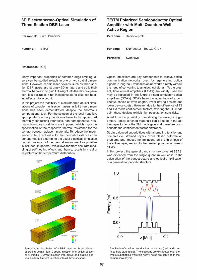
67
3D Electrothermo-Optical Simulation of Three-Section DBR Laser
TE/TM Polarized Semiconductor Optical Amplifier with Multi Quantum Well Active Region
Optical amplifiers are key components in todays optical communication networks, used for regenerating optical signals in long-haul transmission networks directly without the need of converting to an electrical signal. To the pres-ent, fibre optical amplifiers (FOA’s) are widely used but may be replaced in the future by semiconductor optical amplifiers (SOA’s). SOA’s have the advantage of a con-tinuous choice of wavelengths, lower driving powers and lower device costs . However, due to the difference of TE and TM mode confinement factors, favoring the TE mode gain, these devices exhibit high polarization sensitivity.
Apart from the possibility of modifying the waveguide ge-ometry, tensile-strained materials can be used in the ac-tive layer to favor the TM mode gain and therefore com-pensate the confinement factor difference.
Strain-balanced superlattices with alternating tensile- and compressive strained layers avoid plastic deformation problems and impose no limitations on the thickness of the active layer, leading to the desired polarization insen-sitivity.
In this project, the general band structure solver (GEBAS) was extended from the single quantum well case to the calculation of the bandstructure and optical amplification of a general nonperiodic structure.
Amplitude of confined conduction band state (red) and con-fined hole state (blue). The electrons are distributed over the whole superlattice while the heavy-holes are confined in the compressive layers.
Personnel: Ratko Veprek
Funding: SNF 200021-107932 GAIN
Partners: Synopsys
Many important properties of common edge-emitting la-sers can be studied reliably in one or two spatial dimen-sions. However, certain laser devices, such as three-sec-tion DBR lasers, are strongly 3D in nature and so is their thermal behavior. To gain full insight into the device opera-tion, it is desirable, if not indispensable to take self-heat-ing effects into account.
In this project the feasibility of electrothermo-optical simu-lations of tunable multisection lasers in full three dimen-sions has been demonstrated, despite the enormous computational task. For the solution of the local heat flux, appropriate boundary conditions have to be applied. At thermally conducting interfaces, non-homogeneous Neu-mann boundary conditions are imposed, which imply the specification of the respective thermal resistance for the contact between adjacent materials. To reduce the impor-tance of the exact value for the thermal-resistance com-ponent that lies external to the usual electrical simulation domain, as much of the thermal environment as possible is included. In general, this allows for more accurate mod-eling of self-heating effects and, hence, results in a realis-tic picture of the temperature distribution.
Temperature distribution of a DBR laser for three different operating points. Top: Current injection into active section only. Middle: Current injection into active and grating sec-tion. Bottom: Current injection into all three sections.
Personnel: Lutz Schneider
Funding: ETHZ
References: [O8]
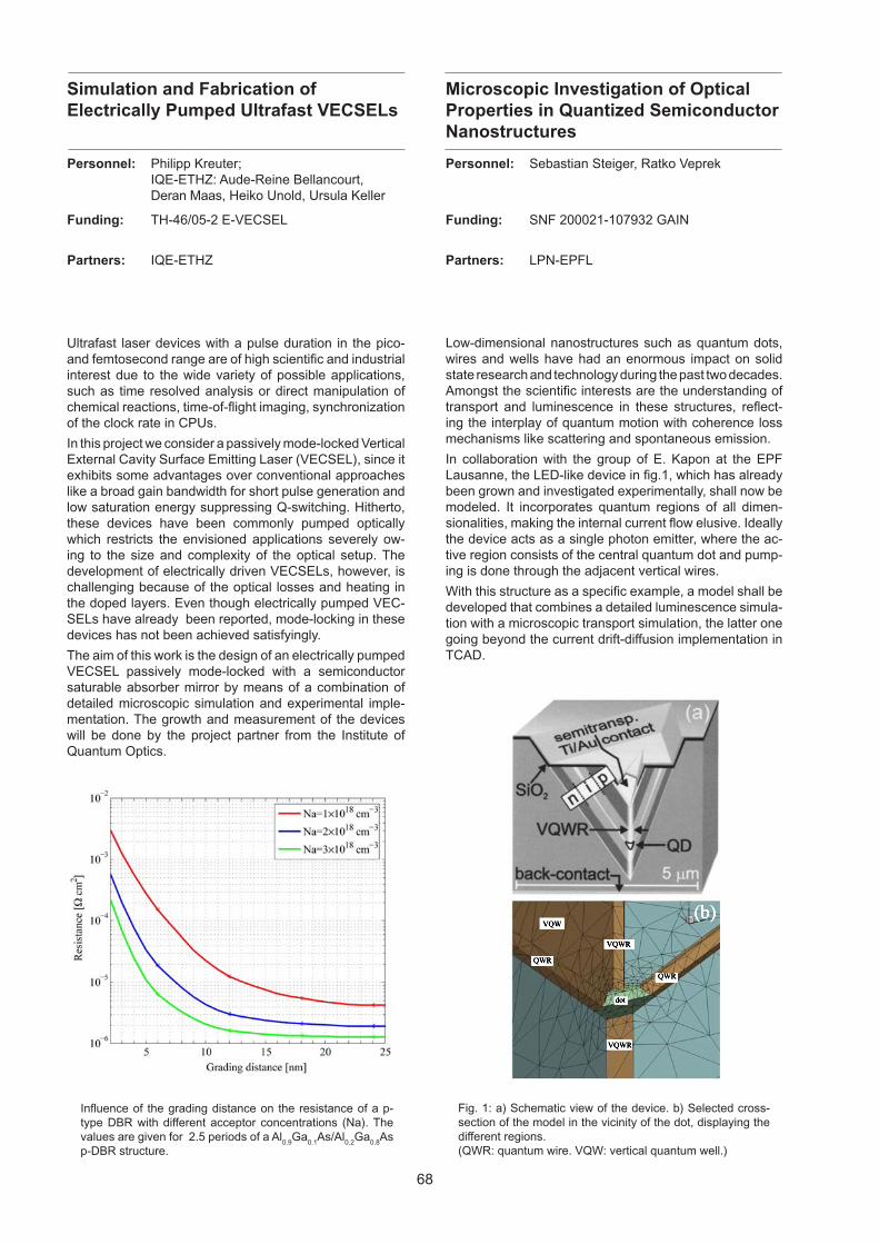
68
Simulation and Fabrication of Electrically Pumped Ultrafast VECSELs
Personnel: Sebastian Steiger, Ratko Veprek
Funding: SNF 200021-107932 GAIN
Partners: LPN-EPFL
Microscopic Investigation of Optical Properties in Quantized Semiconductor Nanostructures
Low-dimensional nanostructures such as quantum dots, wires and wells have had an enormous impact on solid state research and technology during the past two decades. Amongst the scientific interests are the understanding of transport and luminescence in these structures, reflect-ing the interplay of quantum motion with coherence loss mechanisms like scattering and spontaneous emission.
In collaboration with the group of E. Kapon at the EPF Lausanne, the LED-like device in fig.1, which has already been grown and investigated experimentally, shall now be modeled. It incorporates quantum regions of all dimen-sionalities, making the internal current flow elusive. Ideally the device acts as a single photon emitter, where the ac-tive region consists of the central quantum dot and pump-ing is done through the adjacent vertical wires.
With this structure as a specific example, a model shall be developed that combines a detailed luminescence simula-tion with a microscopic transport simulation, the latter one going beyond the current drift-diffusion implementation in TCAD.
Fig. 1: a) Schematic view of the device. b) Selected cross-section of the model in the vicinity of the dot, displaying the different regions.(QWR: quantum wire. VQW: vertical quantum well.)
Ultrafast laser devices with a pulse duration in the pico- and femtosecond range are of high scientific and industrial interest due to the wide variety of possible applications, such as time resolved analysis or direct manipulation of chemical reactions, time-of-flight imaging, synchronization of the clock rate in CPUs.
In this project we consider a passively mode-locked Vertical External Cavity Surface Emitting Laser (VECSEL), since it exhibits some advantages over conventional approaches like a broad gain bandwidth for short pulse generation and low saturation energy suppressing Q-switching. Hitherto, these devices have been commonly pumped optically which restricts the envisioned applications severely ow-ing to the size and complexity of the optical setup. The development of electrically driven VECSELs, however, is challenging because of the optical losses and heating in the doped layers. Even though electrically pumped VEC-SELs have already been reported, mode-locking in these devices has not been achieved satisfyingly.
The aim of this work is the design of an electrically pumped VECSEL passively mode-locked with a semiconductor saturable absorber mirror by means of a combination of detailed microscopic simulation and experimental imple-mentation. The growth and measurement of the devices will be done by the project partner from the Institute of Quantum Optics.
Influence of the grading distance on the resistance of a p-type DBR with different acceptor concentrations (Na). The values are given for 2.5 periods of a Al
0.9Ga
0.1As/Al
0.2Ga
0.8As
p-DBR structure.
Personnel: Philipp Kreuter; IQE-ETHZ: Aude-Reine Bellancourt, Deran Maas, Heiko Unold, Ursula Keller
Funding: TH-46/05-2 E-VECSEL
Partners: IQE-ETHZ

69
Research Projects
Physical Characterization
Coordinator:
Wolfgang Fichtner Mauro Ciappa Dölf Aemmer
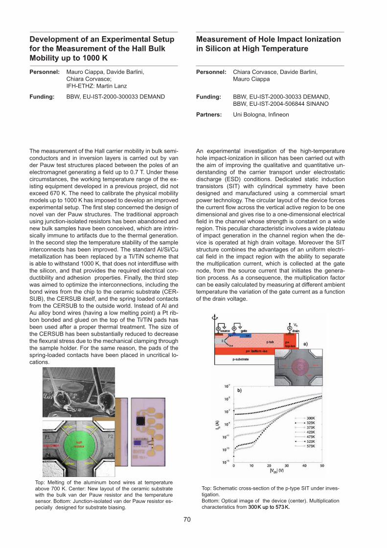
70
Personnel: Mauro Ciappa, Davide Barlini, Chiara Corvasce; IFH-ETHZ: Martin Lanz
Funding: BBW, EU-IST-2000-300033 DEMAND
Development of an Experimental Setup for the Measurement of the Hall Bulk Mobility up to 1000 K
Personnel: Chiara Corvasce, Davide Barlini, Mauro Ciappa
Funding: BBW, EU-IST-2000-30033 DEMAND, BBW, EU-IST-2004-506844 SINANO
Partners: Uni Bologna, Infineon
Measurement of Hole Impact Ionization in Silicon at High Temperature
An experimental investigation of the high-temperature hole impact-ionization in silicon has been carried out with the aim of improving the qualitative and quantitative un-derstanding of the carrier transport under electrostatic discharge (ESD) conditions. Dedicated static induction transistors (SIT) with cylindrical symmetry have been designed and manufactured using a commercial smart power technology. The circular layout of the device forces the current flow across the vertical active region to be one dimensional and gives rise to a one-dimensional electrical field in the channel whose strength is constant on a wide region. This peculiar characteristic involves a wide plateau of impact generation in the channel region when the de-vice is operated at high drain voltage. Moreover the SIT structure combines the advantages of an uniform electri-cal field in the impact region with the ability to separate the multiplication current, which is collected at the gate node, from the source current that initiates the genera-tion process. As a consequence, the multiplication factor can be easily calculated by measuring at different ambient temperature the variation of the gate current as a function of the drain voltage.
Top: Schematic cross-section of the p-type SIT under inves-tigation.Bottom: Optical image of the device (center). Multiplication characteristics from 300K up to 573K.300 K up to 573 K.
The measurement of the Hall carrier mobility in bulk semi-conductors and in inversion layers is carried out by van der Pauw test structures placed between the poles of an electromagnet generating a field up to 0.7 T. Under these circumstances, the working temperature range of the ex-isting equipment developed in a previous project, did not exceed 670 K. The need to calibrate the physical mobility models up to 1000 K has imposed to develop an improved experimental setup. The first step concerned the design of novel van der Pauw structures. The traditional approach using junction-isolated resistors has been abandoned and new bulk samples have been conceived, which are intrin-sically immune to artifacts due to the thermal generation. In the second step the temperature stability of the sample interconnects has been improved. The standard Al/Si/Cu metallization has been replaced by a Ti/TiN scheme that is able to withstand 1000 K, that does not interdiffuse with the silicon, and that provides the required electrical con-ductibility and adhesion properties. Finally, the third step was aimed to optimize the interconnections, including the bond wires from the chip to the ceramic substrate (CER-SUB), the CERSUB itself, and the spring loaded contacts from the CERSUB to the outside world. Instead of Al and Au alloy bond wires (having a low melting point) a Pt rib-bon bonded and glued on the top of the Ti/TiN pads has been used after a proper thermal treatment. The size of the CERSUB has been substantially reduced to decrease the flexural stress due to the mechanical clamping through the sample holder. For the same reason, the pads of the spring-loaded contacts have been placed in uncritical lo-cations.
Top: Melting of the aluminum bond wires at temperature above 700 K. Center: New layout of the ceramic substrate with the bulk van der Pauw resistor and the temperature sensor. Bottom: Junction-isolated van der Pauw resistor es-pecially designed for substrate biasing.
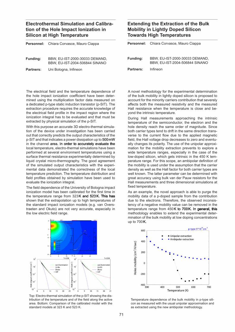
71
Electrothermal Simulation and Calibra-tion of the Hole Impact Ionization in Silicon at High Temperature
Extending the Extraction of the Bulk Mobility in Lightly Doped SiliconTowards High Temperatures
A novel methodology for the experimental determination of the bulk mobility in lightly doped silicon is proposed to account for the minority carriers contribution that severely affects both the measured resistivity and the measured Hall resistance when the temperature is close and be-yond the intrinsic temperature.
During Hall measurements approaching the intrinsic temperature of the semiconductor, the electron and the hole density reach the same order of magnitude. Since both carrier types tend to drift in the same direction trans-verse to the current flow due to the applied magnetic field, the Hall voltage drop decreases to zero and eventu-ally changes its polarity. The use of the unipolar approxi-mation for the mobility extraction prevents to explore a wide temperature ranges, especially in the case of the low-doped silicon, which gets intrinsic in the 450 K tem-perature range. For this scope, an ambipolar definition of the mobility is used under the assumption that the carrier density as well as the Hall factor for both carrier types are well known. The latter parameter can be determined with great accuracy using bulk van der Pauw resistors for the Hall measurements and three dimensional simulations at fixed temperature.
As an example, the novel approach is able to purge the mobility data of a p-doped sample from the contribution due to the electrons. Therefore, the observed inconsis-tency of a negative mobility value can be removed in the temperature range from 450K to 700K. In general, this K to 700K. In general, thisK to 700K. In general, this K. In general, thisK. In general, this methodology enables to extend the experimental deter-mination of the bulk mobility at low doping concentrations up to 700K. K.K.
Temperature dependence of the bulk mobility in p-type sili-con as measured with the usual unipolar approximation and as extracted using the new ambipolar methodology.
Personnel: Chiara Corvasce, Mauro Ciappa
Funding: BBW, EU-IST-2000-30033 DEMAND, BBW, EU-IST-2004-506844 SINANO
Partners: Infineon
The electrical field and the temperature dependence of the hole impact ionization coefficient have been deter-mined using the multiplication factor data measured on a dedicated p-type static induction transistor (p-SIT). The extraction procedure requires the accurate knowledge of the electrical field profile in the impact region where the ionization integral has to be evaluated and that must be extracted by physical simulation of the p-SIT.
With this purpose an accurate 3D electro-thermal simula-tion of the device under investigation has been carried out that correctly predicts the output characteristics of the p-SIT and that indicates a power dissipation up to 500mW500 mW in the channel area. In order to accurately evaluate thearea. In order to accurately evaluate the In order to accurately evaluate the local temperature, electro-thermal simulations have been performed at several environment temperatures using a surface thermal resistance experimentally determined by liquid crystal micro-thermography. The good agreement of the simulated output characteristics with the experi-mental data demonstrated the correctness of the local temperature prediction. The temperature distribution and field profiles obtained by simulation have been used to evaluate the ionization integral.
The field dependence of the University of Bologna impact ionization model has been calibrated for the first time in the temperature range from 323K and 523K. This has K and 523K. This hasK and 523K. This has K. This hasK. This has shown that the extrapolation up to high temperatures of the standard impact ionization models (e.g. van Overs-traeten and Okuto) are not very accurate, especially in the low electric field range.
Personnel: Chiara Corvasce, Mauro Ciappa
Funding: BBW, EU-IST-2000-30033 DEMAND, BBW, EU-IST-2004-506844 SINANO
Partners: Uni Bologna, Infineon
Top: Electro-thermal simulation of the p-SIT showing the dis-tribution of the temperature and of the field along the active area. Bottom: Comparison of the calibrated model with the standard models at 323 K and 523 K.
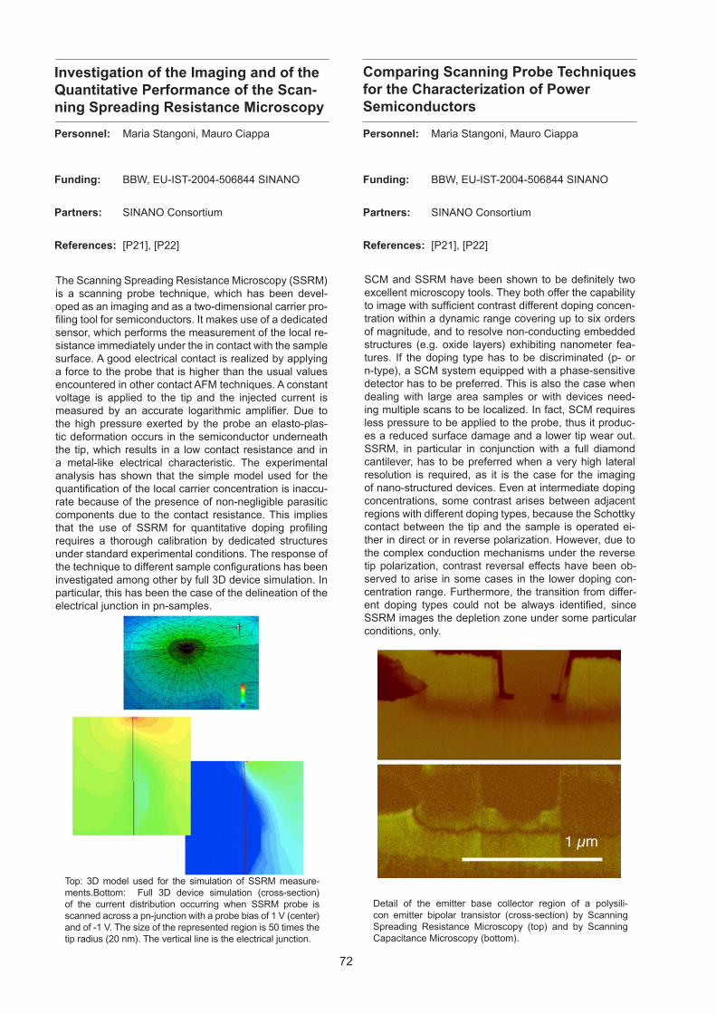
72
Comparing Scanning Probe Techniques for the Characterization of PowerSemiconductors
Personnel: Maria Stangoni, Mauro Ciappa
Funding: BBW, EU-IST-2004-506844 SINANO
Partners: SINANO Consortium
References: [P21], [P22]
SCM and SSRM have been shown to be definitely two excellent microscopy tools. They both offer the capability to image with sufficient contrast different doping concen-tration within a dynamic range covering up to six orders of magnitude, and to resolve non-conducting embedded structures (e.g. oxide layers) exhibiting nanometer fea-tures. If the doping type has to be discriminated (p- or n-type), a SCM system equipped with a phase-sensitive detector has to be preferred. This is also the case when dealing with large area samples or with devices need-ing multiple scans to be localized. In fact, SCM requires less pressure to be applied to the probe, thus it produc-es a reduced surface damage and a lower tip wear out. SSRM, in particular in conjunction with a full diamond cantilever, has to be preferred when a very high lateral resolution is required, as it is the case for the imaging of nano-structured devices. Even at intermediate doping concentrations, some contrast arises between adjacent regions with different doping types, because the Schottky contact between the tip and the sample is operated ei-ther in direct or in reverse polarization. However, due to the complex conduction mechanisms under the reverse tip polarization, contrast reversal effects have been ob-served to arise in some cases in the lower doping con-centration range. Furthermore, the transition from differ-ent doping types could not be always identified, since SSRM images the depletion zone under some particular conditions, only.
Personnel: Maria Stangoni, Mauro Ciappa
Funding: BBW, EU-IST-2004-506844 SINANO
Partners: SINANO Consortium
References: [P21], [P22]
Investigation of the Imaging and of the Quantitative Performance of the Scan-ning Spreading Resistance Microscopy
The Scanning Spreading Resistance Microscopy (SSRM) is a scanning probe technique, which has been devel-oped as an imaging and as a two-dimensional carrier pro-filing tool for semiconductors. It makes use of a dedicated sensor, which performs the measurement of the local re-sistance immediately under the in contact with the sample surface. A good electrical contact is realized by applying a force to the probe that is higher than the usual values encountered in other contact AFM techniques. A constant voltage is applied to the tip and the injected current is measured by an accurate logarithmic amplifier. Due to the high pressure exerted by the probe an elasto-plas-tic deformation occurs in the semiconductor underneath the tip, which results in a low contact resistance and in a metal-like electrical characteristic. The experimental analysis has shown that the simple model used for the quantification of the local carrier concentration is inaccu-rate because of the presence of non-negligible parasitic components due to the contact resistance. This implies that the use of SSRM for quantitative doping profiling requires a thorough calibration by dedicated structures under standard experimental conditions. The response of the technique to different sample configurations has been investigated among other by full 3D device simulation. In particular, this has been the case of the delineation of the electrical junction in pn-samples.
Detail of the emitter base collector region of a polysili-con emitter bipolar transistor (cross-section) by Scanning Spreading Resistance Microscopy (top) and by Scanning Capacitance Microscopy (bottom).
Top: 3D model used for the simulation of SSRM measure-ments.Bottom: Full 3D device simulation (cross-section) of the current distribution occurring when SSRM probe is scanned across a pn-junction with a probe bias of 1 V (center) and of -1 V. The size of the represented region is 50 times the tip radius (20 nm). The vertical line is the electrical junction.
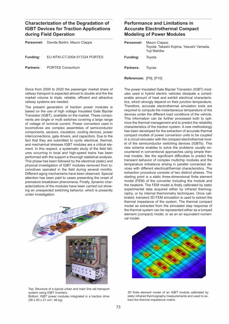
73
Personnel: Mauro Ciappa; Toyota: Takashi Kojima, Yasushi Yamada, Yuji Nishibe
Funding: Toyota
Partners: Toyota
References: [P9], [P10]
Performance and Limitations in Accurate Electrothermal Compact Modeling of Power Modules
The power Insulated Gate Bipolar Transistor (IGBT) mod-ules used in hybrid electric vehicles dissipate a consid-erable amount of heat and exhibit electrical characteris-tics, which strongly depend on their junction temperature. Therefore, accurate electrothermal simulation tools are required to compute the instantaneous temperature of the devices under the different load conditions of the vehicle. This information can be further processed both to opti-mize the thermal management and to predict the reliability characteristics of the traction system. A new methodology has been developed for the extraction of accurate thermal compact models of power conversion units to be coupled in a circuit simulator with the compact electrothermal mod-el of the semiconductor switching devices (IGBTs). This new scheme enables to solve the problems usually en-countered in conventional approaches using simple ther-mal models, like the significant difficulties to predict the transient behavior of complex multichip modules and the temperature imbalance arising in parallel connected de-vices with different electrical/thermal characteristics. The extraction procedure consists of two distinct phases. The starting point is a static three-dimensional finite element model (FEM) of the converter including the module and the heatsink. The FEM model is firstly calibrated by static experimental data acquired either by infrared thermog-raphy, or by internal thermometry techniques. Once cali-brated, transient 3D FEM simulation is used to extract the thermal impedance of the system. The thermal compact model as extracted from the simulated step response of the thermal system can be represented either as a lumped element (compact) model, or as an an equivalent numeri-cal model.
3D finite element model of an IGBT module calibrated by static infrared thermography measurements and used to ex-tract the thermal impedence matrix.
Personnel: Davide Barlini, Mauro Ciappa
Funding: EU MTKI-CT-2004-517224 PORTES
Partners: PORTES Consortium
Characterization of the Degradation of IGBT Devices for Traction Applications during Field Operation
Since from 2000 to 2020 the passenger market share of railway transport is expected almost to double and the the market volume to triple, reliable, efficient and attractive railway systems are needed.
The present generation of traction power modules is based on the use of high voltage Insulated Gate Bipolar Transistor (IGBT), available on the market. These compo-nents are single or multi switches covering a large range of voltage of nominal current. Power converters used in locomotives are complex assemblies of semiconductor components, sensors, insulators, cooling devices, power interconnections, gate drivers, and capacitors. Due to the fact that they are submitted to cyclic electrical, thermal, and mechanical stresses IGBT modules are a critical ele-ment. In this respect, a systematic study of the field fail-ures occurring in local and high-speed trains has been performed with the support a thourogh statistical analysis. This phase has been followed by the electrical (static) and physical investigation of IGBT modules removed from lo-comotives operated in the field during several months. Different aging mechanisms have been observed. Special attention has been paid to cases presenting the onset of premature breakdown phenomena. Finally, dynamic char-acterizations of the modules have been carried out show-ing an unexpected switching behavior, which is presently under investigation.
Top: Structure of a typical urban and main line rail transport system using IGBT inverters. Bottom: IGBT power modules integrated in a traction drive (56 x 50 x 21 cm3, 46 kg)
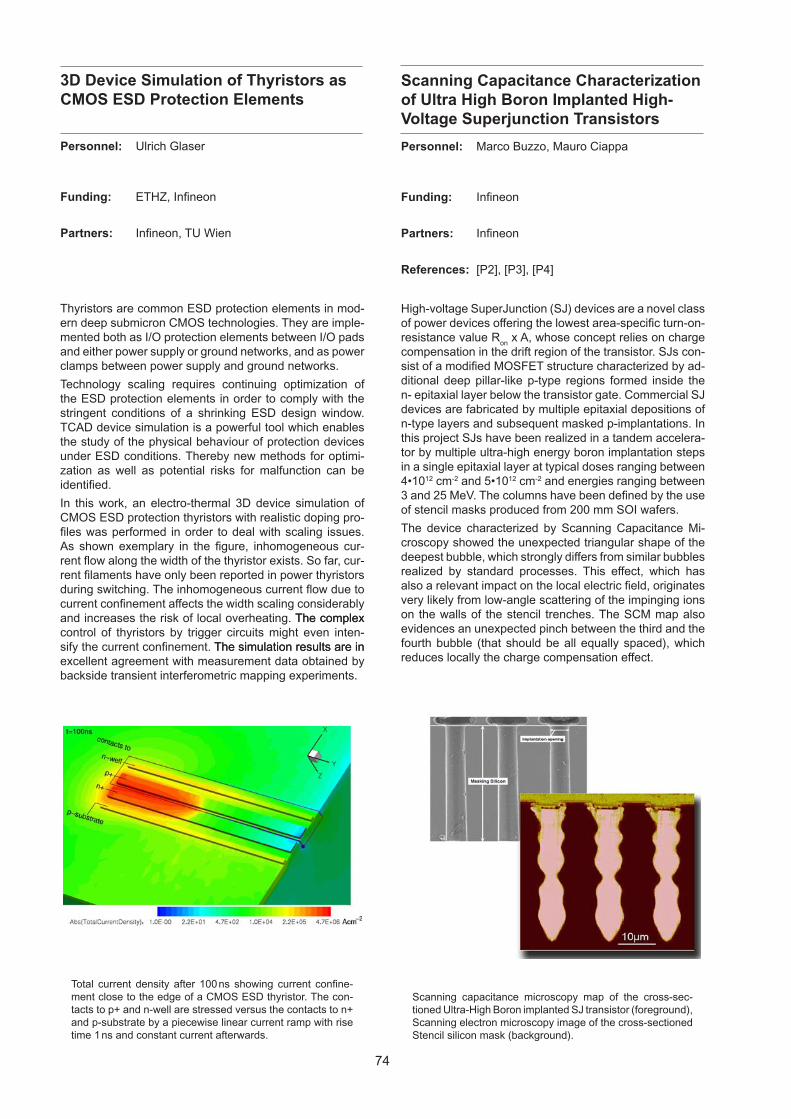
74
3D Device Simulation of Thyristors as CMOS ESD Protection Elements
Thyristors are common ESD protection elements in mod-ern deep submicron CMOS technologies. They are imple-mented both as I/O protection elements between I/O pads and either power supply or ground networks, and as power clamps between power supply and ground networks.
Technology scaling requires continuing optimization of the ESD protection elements in order to comply with the stringent conditions of a shrinking ESD design window. TCAD device simulation is a powerful tool which enables the study of the physical behaviour of protection devices under ESD conditions. Thereby new methods for optimi-zation as well as potential risks for malfunction can be identified.
In this work, an electro-thermal 3D device simulation of CMOS ESD protection thyristors with realistic doping pro-files was performed in order to deal with scaling issues. As shown exemplary in the figure, inhomogeneous cur-rent flow along the width of the thyristor exists. So far, cur-rent filaments have only been reported in power thyristors during switching. The inhomogeneous current flow due to current confinement affects the width scaling considerably and increases the risk of local overheating. The complexThe complex control of thyristors by trigger circuits might even inten-sify the current confinement. The simulation results are inThe simulation results are in excellent agreement with measurement data obtained by backside transient interferometric mapping experiments.
Total current density after 100 ns showing current confine-ment close to the edge of a CMOS ESD thyristor. The con-tacts to p+ and n-well are stressed versus the contacts to n+ and p-substrate by a piecewise linear current ramp with rise time 1 ns and constant current afterwards.
Personnel: Ulrich Glaser
Funding: ETHZ, Infineon
Partners: Infineon, TU Wien
Personnel: Marco Buzzo, Mauro Ciappa
Funding: Infineon
Partners: Infineon
References: [P2], [P3], [P4]
Scanning Capacitance Characterization of Ultra High Boron Implanted High-Voltage Superjunction Transistors
High-voltage SuperJunction (SJ) devices are a novel class of power devices offering the lowest area-specific turn-on-resistance value R
on x A, whose concept relies on charge
compensation in the drift region of the transistor. SJs con-sist of a modified MOSFET structure characterized by ad-ditional deep pillar-like p-type regions formed inside the n- epitaxial layer below the transistor gate. Commercial SJ devices are fabricated by multiple epitaxial depositions of n-type layers and subsequent masked p-implantations. In this project SJs have been realized in a tandem accelera-tor by multiple ultra-high energy boron implantation steps in a single epitaxial layer at typical doses ranging between 4•1012 cm-2 and 5•1012 cm-2 and energies ranging between 3 and 25 MeV. The columns have been defined by the use of stencil masks produced from 200 mm SOI wafers.
The device characterized by Scanning Capacitance Mi-croscopy showed the unexpected triangular shape of the deepest bubble, which strongly differs from similar bubbles realized by standard processes. This effect, which has also a relevant impact on the local electric field, originates very likely from low-angle scattering of the impinging ions on the walls of the stencil trenches. The SCM map also evidences an unexpected pinch between the third and the fourth bubble (that should be all equally spaced), which reduces locally the charge compensation effect.
Scanning capacitance microscopy map of the cross-sec-tioned Ultra-High Boron implanted SJ transistor (foreground), Scanning electron microscopy image of the cross-sectioned Stencil silicon mask (background).
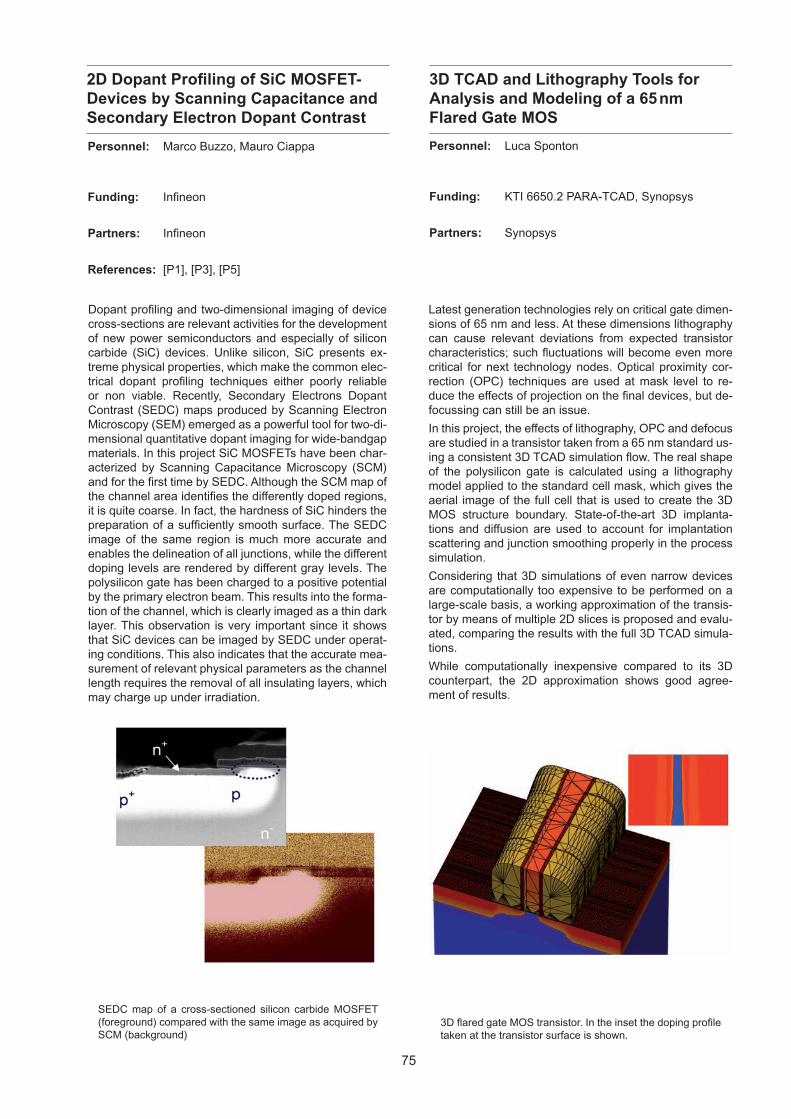
75
2D Dopant Profiling of SiC MOSFET-Devices by Scanning Capacitance and Secondary Electron Dopant Contrast
3D TCAD and Lithography Tools for Analysis and Modeling of a 65 nm Flared Gate MOS
Latest generation technologies rely on critical gate dimen-sions of 65 nm and less. At these dimensions lithography can cause relevant deviations from expected transistor characteristics; such fluctuations will become even more critical for next technology nodes. Optical proximity cor-rection (OPC) techniques are used at mask level to re-duce the effects of projection on the final devices, but de-focussing can still be an issue.
In this project, the effects of lithography, OPC and defocus are studied in a transistor taken from a 65 nm standard us-ing a consistent 3D TCAD simulation flow. The real shape of the polysilicon gate is calculated using a lithography model applied to the standard cell mask, which gives the aerial image of the full cell that is used to create the 3D MOS structure boundary. State-of-the-art 3D implanta-tions and diffusion are used to account for implantation scattering and junction smoothing properly in the process simulation.
Considering that 3D simulations of even narrow devices are computationally too expensive to be performed on a large-scale basis, a working approximation of the transis-tor by means of multiple 2D slices is proposed and evalu-ated, comparing the results with the full 3D TCAD simula-tions.
While computationally inexpensive compared to its 3D counterpart, the 2D approximation shows good agree-ment of results.
3D flared gate MOS transistor. In the inset the doping profile taken at the transistor surface is shown.
Personnel: Luca Sponton
Funding: KTI 6650.2 PARA-TCAD, Synopsys
Partners: Synopsys
Personnel: Marco Buzzo, Mauro Ciappa
Funding: Infineon
Partners: Infineon
References: [P1], [P3], [P5]
Dopant profiling and two-dimensional imaging of device cross-sections are relevant activities for the development of new power semiconductors and especially of silicon carbide (SiC) devices. Unlike silicon, SiC presents ex-treme physical properties, which make the common elec-trical dopant profiling techniques either poorly reliable or non viable. Recently, Secondary Electrons Dopant Contrast (SEDC) maps produced by Scanning Electron Microscopy (SEM) emerged as a powerful tool for two-di-mensional quantitative dopant imaging for wide-bandgap materials. In this project SiC MOSFETs have been char-acterized by Scanning Capacitance Microscopy (SCM) and for the first time by SEDC. Although the SCM map of the channel area identifies the differently doped regions, it is quite coarse. In fact, the hardness of SiC hinders the preparation of a sufficiently smooth surface. The SEDC image of the same region is much more accurate and enables the delineation of all junctions, while the different doping levels are rendered by different gray levels. The polysilicon gate has been charged to a positive potential by the primary electron beam. This results into the forma-tion of the channel, which is clearly imaged as a thin dark layer. This observation is very important since it shows that SiC devices can be imaged by SEDC under operat-ing conditions. This also indicates that the accurate mea-surement of relevant physical parameters as the channel length requires the removal of all insulating layers, which may charge up under irradiation.
SEDC map of a cross-sectioned silicon carbide MOSFET (foreground) compared with the same image as acquired by SCM (background)
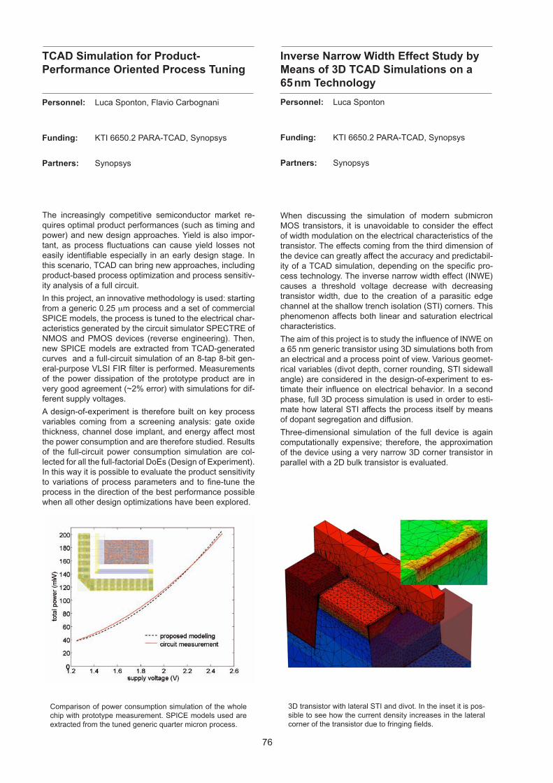
76
TCAD Simulation for Product-Performance Oriented Process Tuning
Inverse Narrow Width Effect Study by Means of 3D TCAD Simulations on a 65 nm Technology
When discussing the simulation of modern submicron MOS transistors, it is unavoidable to consider the effect of width modulation on the electrical characteristics of the transistor. The effects coming from the third dimension of the device can greatly affect the accuracy and predictabil-ity of a TCAD simulation, depending on the specific pro-cess technology. The inverse narrow width effect (INWE) causes a threshold voltage decrease with decreasing transistor width, due to the creation of a parasitic edge channel at the shallow trench isolation (STI) corners. This phenomenon affects both linear and saturation electrical characteristics.
The aim of this project is to study the influence of INWE on a 65 nm generic transistor using 3D simulations both from an electrical and a process point of view. Various geomet-rical variables (divot depth, corner rounding, STI sidewall angle) are considered in the design-of-experiment to es-timate their influence on electrical behavior. In a second phase, full 3D process simulation is used in order to esti-mate how lateral STI affects the process itself by means of dopant segregation and diffusion.
Three-dimensional simulation of the full device is again computationally expensive; therefore, the approximation of the device using a very narrow 3D corner transistor in parallel with a 2D bulk transistor is evaluated.
3D transistor with lateral STI and divot. In the inset it is pos-sible to see how the current density increases in the lateral corner of the transistor due to fringing fields.
Personnel: Luca Sponton
Funding: KTI 6650.2 PARA-TCAD, Synopsys
Partners: Synopsys
The increasingly competitive semiconductor market re-quires optimal product performances (such as timing and power) and new design approaches. Yield is also impor-tant, as process fluctuations can cause yield losses not easily identifiable especially in an early design stage. In this scenario, TCAD can bring new approaches, including product-based process optimization and process sensitiv-ity analysis of a full circuit.
In this project, an innovative methodology is used: starting from a generic 0.25 mm process and a set of commercial SPICE models, the process is tuned to the electrical char-acteristics generated by the circuit simulator SPECTRE of NMOS and PMOS devices (reverse engineering). Then, new SPICE models are extracted from TCAD-generated curves and a full-circuit simulation of an 8-tap 8-bit gen-eral-purpose VLSI FIR filter is performed. Measurements of the power dissipation of the prototype product are in very good agreement (~2% error) with simulations for dif-ferent supply voltages.
A design-of-experiment is therefore built on key process variables coming from a screening analysis: gate oxide thickness, channel dose implant, and energy affect most the power consumption and are therefore studied. Results of the full-circuit power consumption simulation are col-lected for all the full-factorial DoEs (Design of Experiment). In this way it is possible to evaluate the product sensitivity to variations of process parameters and to fine-tune the process in the direction of the best performance possible when all other design optimizations have been explored.
Comparison of power consumption simulation of the whole chip with prototype measurement. SPICE models used are extracted from the tuned generic quarter micron process.
Personnel: Luca Sponton, Flavio Carbognani
Funding: KTI 6650.2 PARA-TCAD, Synopsys
Partners: Synopsys
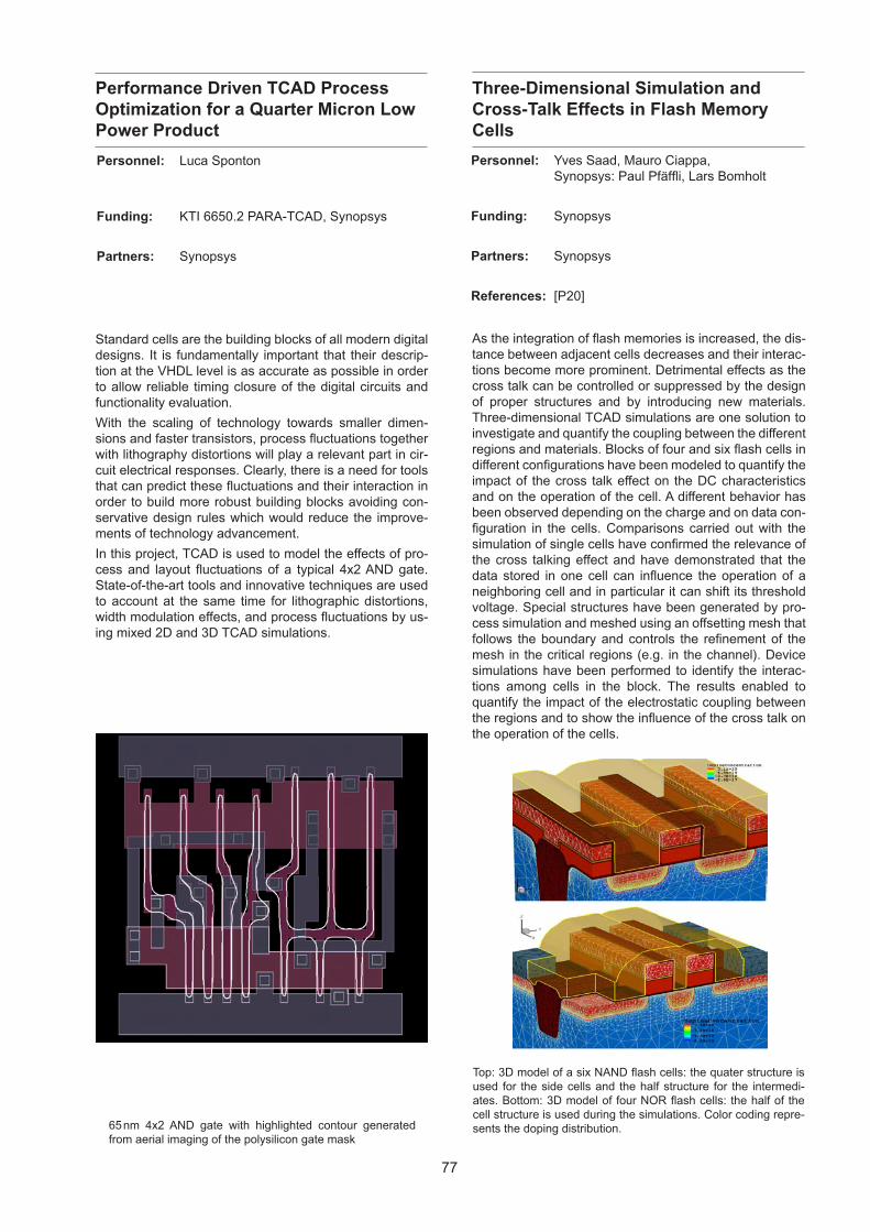
77
Performance Driven TCAD Process Optimization for a Quarter Micron LowPower Product
Three-Dimensional Simulation and Cross-Talk Effects in Flash Memory Cells
Personnel: Yves Saad, Mauro Ciappa, Synopsys: Paul Pfäffli, Lars Bomholt
Funding: Synopsys
Partners: Synopsys
References: [P20]
As the integration of flash memories is increased, the dis-tance between adjacent cells decreases and their interac-tions become more prominent. Detrimental effects as the cross talk can be controlled or suppressed by the design of proper structures and by introducing new materials. Three-dimensional TCAD simulations are one solution to investigate and quantify the coupling between the different regions and materials. Blocks of four and six flash cells in different configurations have been modeled to quantify the impact of the cross talk effect on the DC characteristics and on the operation of the cell. A different behavior has been observed depending on the charge and on data con-figuration in the cells. Comparisons carried out with the simulation of single cells have confirmed the relevance of the cross talking effect and have demonstrated that the data stored in one cell can influence the operation of a neighboring cell and in particular it can shift its threshold voltage. Special structures have been generated by pro-cess simulation and meshed using an offsetting mesh that follows the boundary and controls the refinement of the mesh in the critical regions (e.g. in the channel). Device simulations have been performed to identify the interac-tions among cells in the block. The results enabled to quantify the impact of the electrostatic coupling between the regions and to show the influence of the cross talk on the operation of the cells.
Top: 3D model of a six NAND flash cells: the quater structure is used for the side cells and the half structure for the intermedi-ates. Bottom: 3D model of four NOR flash cells: the half of the cell structure is used during the simulations. Color coding repre-sents the doping distribution.
Standard cells are the building blocks of all modern digital designs. It is fundamentally important that their descrip-tion at the VHDL level is as accurate as possible in order to allow reliable timing closure of the digital circuits and functionality evaluation.
With the scaling of technology towards smaller dimen-sions and faster transistors, process fluctuations together with lithography distortions will play a relevant part in cir-cuit electrical responses. Clearly, there is a need for tools that can predict these fluctuations and their interaction in order to build more robust building blocks avoiding con-servative design rules which would reduce the improve-ments of technology advancement.
In this project, TCAD is used to model the effects of pro-cess and layout fluctuations of a typical 4x2 AND gate. State-of-the-art tools and innovative techniques are used to account at the same time for lithographic distortions, width modulation effects, and process fluctuations by us-ing mixed 2D and 3D TCAD simulations.
65 nm 4x2 AND gate with highlighted contour generated from aerial imaging of the polysilicon gate mask
Personnel: Luca Sponton
Funding: KTI 6650.2 PARA-TCAD, Synopsys
Partners: Synopsys
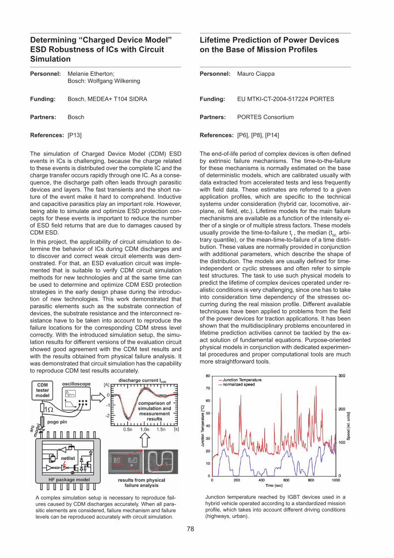
78
Personnel: Melanie Etherton; Bosch: Wolfgang Wilkening
Funding: Bosch, MEDEA+ T104 SIDRA
Partners: Bosch
References: [P13]
Determining “Charged Device Model” ESD Robustness of ICs with Circuit Simulation
The simulation of Charged Device Model (CDM) ESD events in ICs is challenging, because the charge related to these events is distributed over the complete IC and the charge transfer occurs rapidly through one IC. As a conse-quence, the discharge path often leads through parasitic devices and layers. The fast transients and the short na-ture of the event make it hard to comprehend. Inductive and capacitive parasitics play an important role. However, being able to simulate and optimize ESD protection con-cepts for these events is important to reduce the number of ESD field returns that are due to damages caused by CDM ESD.
In this project, the applicability of circuit simulation to de-termine the behavior of ICs during CDM discharges and to discover and correct weak circuit elements was dem-onstrated. For that, an ESD evaluation circuit was imple-mented that is suitable to verify CDM circuit simulation methods for new technologies and at the same time can be used to determine and optimize CDM ESD protection strategies in the early design phase during the introduc-tion of new technologies. This work demonstrated that parasitic elements such as the substrate connection of devices, the substrate resistance and the interconnect re-sistance have to be taken into account to reproduce the failure locations for the corresponding CDM stress level correctly. With the introduced simulation setup, the simu-lation results for different versions of the evaluation circuit showed good agreement with the CDM test results and with the results obtained from physical failure analysis. It was demonstrated that circuit simulation has the capability to reproduce CDM test results accurately.
A complex simulation setup is necessary to reproduce fail-ures caused by CDM discharges accurately. When all para-sitic elements are considered, failure mechanism and failure levels can be reproduced accurately with circuit simulation.
Personnel: Mauro Ciappa
Funding: EU MTKI-CT-2004-517224 PORTES
Partners: PORTES Consortium
References: [P6], [P8], [P14]
Lifetime Prediction of Power Devices on the Base of Mission Profiles
The end-of-life period of complex devices is often defined by extrinsic failure mechanisms. The time-to-the-failure for these mechanisms is normally estimated on the base of deterministic models, which are calibrated usually with data extracted from accelerated tests and less frequently with field data. These estimates are referred to a given application profiles, which are specific to the technical systems under consideration (hybrid car, locomotive, air-plane, oil field, etc.). Lifetime models for the main failure mechanisms are available as a function of the intensity ei-ther of a single or of multiple stress factors. These models usually provide the time-to-failure t
f , the median (t
50, arbi-
trary quantile), or the mean-time-to-failure of a time distri-bution. These values are normally provided in conjunction with additional parameters, which describe the shape of the distribution. The models are usually defined for time-independent or cyclic stresses and often refer to simple test structures. The task to use such physical models to predict the lifetime of complex devices operated under re-alistic conditions is very challenging, since one has to take into consideration time dependency of the stresses oc-curring during the real mission profile. Different available techniques have been applied to problems from the field of the power devices for traction applications. It has been shown that the multidisciplinary problems encountered in lifetime prediction activities cannot be tackled by the ex-act solution of fundamental equations. Purpose-oriented physical models in conjunction with dedicated experimen-tal procedures and proper computational tools are much more straightforward tools.
Junction temperature reached by IGBT devices used in a hybrid vehicle operated according to a standardized mission profile, which takes into account different driving conditions (highways, urban).

79
Research Projects
Bio-Electromagnetics and Electromagnetic Compatibility
Coordinator:
Niels Kuster
(Adjunct Professor, Department of Information Technology and Electrical Engineering)
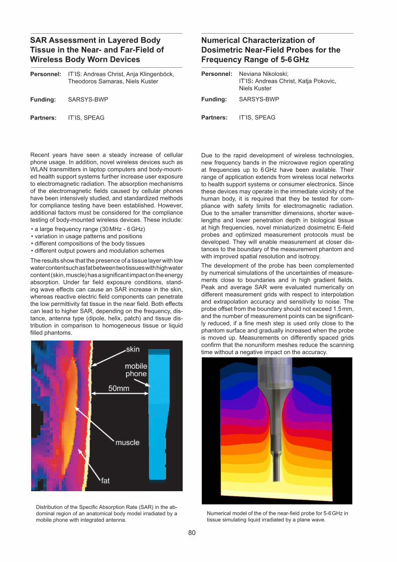
80
SAR Assessment in Layered Body Tissue in the Near- and Far-Field of Wireless Body Worn Devices
Numerical Characterization of Dosimetric Near-Field Probes for the Frequency Range of 5-6 GHz
Recent years have seen a steady increase of cellular phone usage. In addition, novel wireless devices such as WLAN transmitters in laptop computers and body-mount-ed health support systems further increase user exposure to electromagnetic radiation. The absorption mechanisms of the electromagnetic fields caused by cellular phones have been intensively studied, and standardized methods for compliance testing have been established. However, additional factors must be considered for the compliance testing of body-mounted wireless devices. These include:
• a large frequency range (30 MHz - 6 GHz)• variation in usage patterns and positions• different compositions of the body tissues• different output powers and modulation schemes
The results show that the presence of a tissue layer with low water content such as fat between two tissues with high water content (skin, muscle) has a significant impact on the energy absorption. Under far field exposure conditions, stand-ing wave effects can cause an SAR increase in the skin, whereas reactive electric field components can penetrate the low permittivity fat tissue in the near field. Both effects can lead to higher SAR, depending on the frequency, dis-tance, antenna type (dipole, helix, patch) and tissue dis-tribution in comparison to homogeneous tissue or liquid filled phantoms.
Distribution of the Specific Absorption Rate (SAR) in the ab-dominal region of an anatomical body model irradiated by a mobile phone with integrated antenna.
Personnel: IT’IS: Andreas Christ, Anja Klingenböck, Theodoros Samaras, Niels Kuster
Funding: SARSYS-BWP
Partners: IT’IS, SPEAG
Due to the rapid development of wireless technologies, new frequency bands in the microwave region operating at frequencies up to 6 GHz have been available. Their range of application extends from wireless local networks to health support systems or consumer electronics. Since these devices may operate in the immediate vicinity of the human body, it is required that they be tested for com-pliance with safety limits for electromagnetic radiation. Due to the smaller transmitter dimensions, shorter wave-lengths and lower penetration depth in biological tissue at high frequencies, novel miniaturized dosimetric E-field probes and optimized measurement protocols must be developed. They will enable measurement at closer dis-tances to the boundary of the measurement phantom and with improved spatial resolution and isotropy.
The development of the probe has been complemented by numerical simulations of the uncertainties of measure-ments close to boundaries and in high gradient fields. Peak and average SAR were evaluated numerically on different measurement grids with respect to interpolation and extrapolation accuracy and sensitivity to noise. The probe offset from the boundary should not exceed 1.5 mm, and the number of measurement points can be significant-ly reduced, if a fine mesh step is used only close to the phantom surface and gradually increased when the probe is moved up. Measurements on differently spaced grids confirm that the nonuniform meshes reduce the scanning time without a negative impact on the accuracy.
Numerical model of the of the near-field probe for 5-6 GHz in tissue simulating liquid irradiated by a plane wave.
Personnel: Neviana Nikoloski; IT’IS: Andreas Christ, Katja Pokovic, Niels Kuster
Funding: SARSYS-BWP
Partners: IT’IS, SPEAG
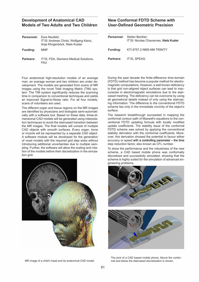
81
Development of Anatomical CADModels of Two Adults and Two Children
New Conformal FDTD Scheme with User-Defined Geometric Precision
Four anatomical high-resolution models of an average man, an average woman and two children are under de-velopment. The models are generated from scans of MR images using the novel Total Imaging Matrix (TIM) sys-tem. The TIM system significantly reduces the scanning time in comparison to conventional techniques and yields an improved Signal-to-Noise ratio. For all four models, scans of volunteers are used.
The different organ and tissue regions on the MR images are identified by physicians and biologists semi-automati-cally with a software tool. Based on these data, three-di-mensional CAD models will be generated using interpola-tion techniques to avoid the staircased transition between the MR images. The final models will consist of multiple CAD objects with smooth surfaces. Every organ, bone or muscle will be represented by a separate CAD object. A software module will be developed for the generation of voxel models with the required grid step sizes without introducing additional uncertainties due to multiple sam-pling. Further, the software will allow the scaling and rota-tion of the models before their discretization in the simula-tion grid.
MR image of a child’s head and its anatomical CAD model.
Personnel: Esra Neufeld; IT’IS: Andreas Christ, Wolfgang Kainz, Anja Klingenböck, Niels Kuster
Funding: MMF
Partners: IT’IS, FDA, Siemens Medical Solutions, FAU
During the past decade the finite-difference time-domain (FDTD) method has become a popular method for electro-magnetic computations. However, a well known deficiency is that grid non-aligned object surfaces can lead to inac-curacies in electromagnetic simulations due to the stair-cased meshing. The deficiency can be overcome by using all geometrical details instead of only using the staircas-ing information. The difference to the conventional FDTD scheme lies only in the immediate vincinity of the object’s surface.
The research breakthrough succeeded in mapping the conformal contour path of Maxwell’s equations to the con-ventional FDTD updating formula with locally modified update coefficients. The stability issue of the conformal FDTD scheme was solved by applying the conventional stability derivation with the conformal coefficients. More-over, this derivation showed the potential to favour either accuracy or speed with a controlling parameter – the time with a controlling parameter – the time step reduction factor, also known as CFL number.
To show the performance and the robustness of the new scheme, a CAD based mobile phone was conformally discretized and successfully simulated, showing that the scheme is highly suited for the simulation of advanced en-gineering problems.
The joint of a CAD based mobile phone. Above the confor-mal and below the staircased discretization is shown.
Personnel: Stefan Benkler; IT’IS: Nicolas Chavannes, Niels KusterNiels Kuster
Funding: KTI 6757.2 NMS-NM TRINITY
Partners: IT’IS, SPEAG
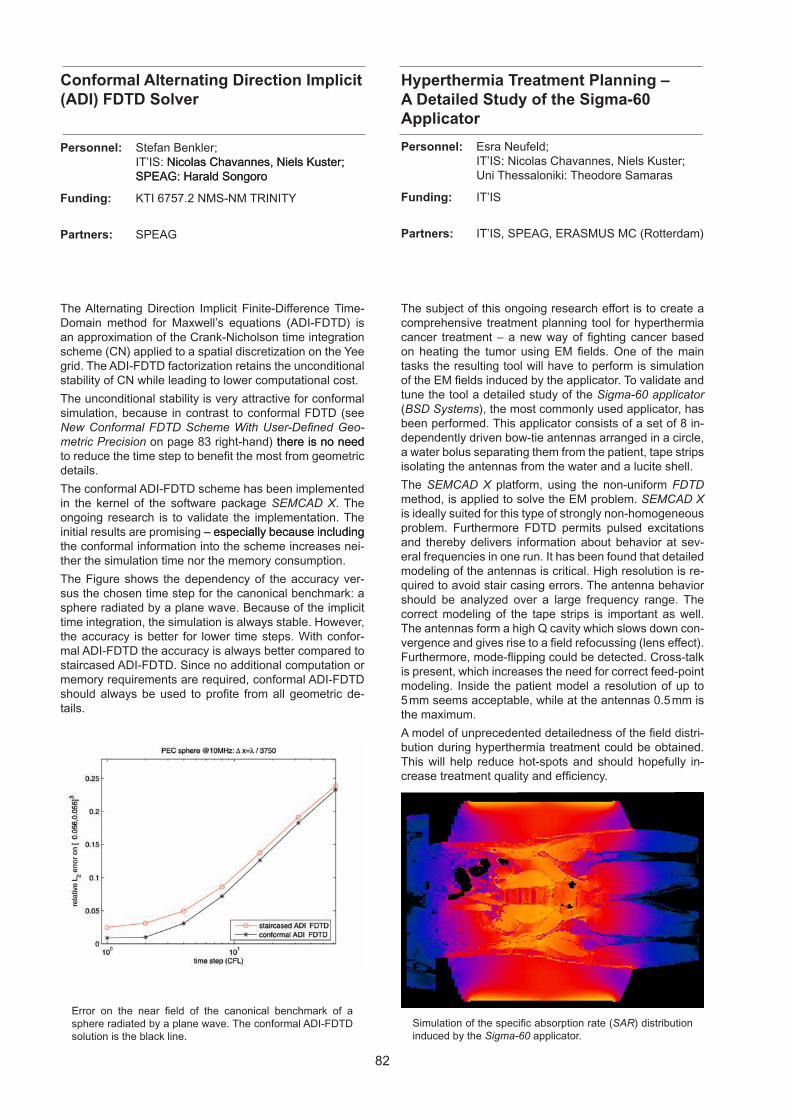
82
Conformal Alternating Direction Implicit (ADI) FDTD Solver
Personnel: Esra Neufeld; IT’IS: Nicolas Chavannes, Niels Kuster; Uni Thessaloniki: Theodore Samaras
Funding: IT’IS
Partners: IT’IS, SPEAG, ERASMUS MC (Rotterdam)
Hyperthermia Treatment Planning – A Detailed Study of the Sigma-60 Applicator
The Alternating Direction Implicit Finite-Difference Time-Domain method for Maxwell’s equations (ADI-FDTD) is an approximation of the Crank-Nicholson time integration scheme (CN) applied to a spatial discretization on the Yee grid. The ADI-FDTD factorization retains the unconditional stability of CN while leading to lower computational cost.
The unconditional stability is very attractive for conformal simulation, because in contrast to conformal FDTD (see New Conformal FDTD Scheme With User-Defined Geo-metric Precision on page 83 right-hand) there is no needthere is no need to reduce the time step to benefit the most from geometric details.
The conformal ADI-FDTD scheme has been implemented in the kernel of the software package SEMCAD X. The ongoing research is to validate the implementation. The initial results are promising – especially because including – especially because including the conformal information into the scheme increases nei-ther the simulation time nor the memory consumption.
The Figure shows the dependency of the accuracy ver-sus the chosen time step for the canonical benchmark: a sphere radiated by a plane wave. Because of the implicit time integration, the simulation is always stable. However, the accuracy is better for lower time steps. With confor-mal ADI-FDTD the accuracy is always better compared to staircased ADI-FDTD. Since no additional computation or memory requirements are required, conformal ADI-FDTD should always be used to profite from all geometric de-tails.
Error on the near field of the canonical benchmark of a sphere radiated by a plane wave. The conformal ADI-FDTD solution is the black line.
Personnel: Stefan Benkler; IT’IS: Nicolas Chavannes, Niels Kuster;Nicolas Chavannes, Niels Kuster; SPEAG: Harald SongoroSPEAG: Harald Songoro
Funding: KTI 6757.2 NMS-NM TRINITY
Partners: SPEAG
The subject of this ongoing research effort is to create a comprehensive treatment planning tool for hyperthermia cancer treatment – a new way of fighting cancer based on heating the tumor using EM fields. One of the main tasks the resulting tool will have to perform is simulation of the EM fields induced by the applicator. To validate and tune the tool a detailed study of the Sigma-60 applicator (BSD Systems), the most commonly used applicator, has been performed. This applicator consists of a set of 8 in-dependently driven bow-tie antennas arranged in a circle, a water bolus separating them from the patient, tape strips isolating the antennas from the water and a lucite shell.
The SEMCAD X platform, using the non-uniform FDTD method, is applied to solve the EM problem. SEMCAD X is ideally suited for this type of strongly non-homogeneous problem. Furthermore FDTD permits pulsed excitations and thereby delivers information about behavior at sev-eral frequencies in one run. It has been found that detailed modeling of the antennas is critical. High resolution is re-quired to avoid stair casing errors. The antenna behavior should be analyzed over a large frequency range. The correct modeling of the tape strips is important as well. The antennas form a high Q cavity which slows down con-vergence and gives rise to a field refocussing (lens effect). Furthermore, mode-flipping could be detected. Cross-talk is present, which increases the need for correct feed-point modeling. Inside the patient model a resolution of up to 5 mm seems acceptable, while at the antennas 0.5 mm is the maximum.
A model of unprecedented detailedness of the field distri-bution during hyperthermia treatment could be obtained. This will help reduce hot-spots and should hopefully in-crease treatment quality and efficiency.
Simulation of the specific absorption rate (SAR) distribution induced by the Sigma-60 applicator.
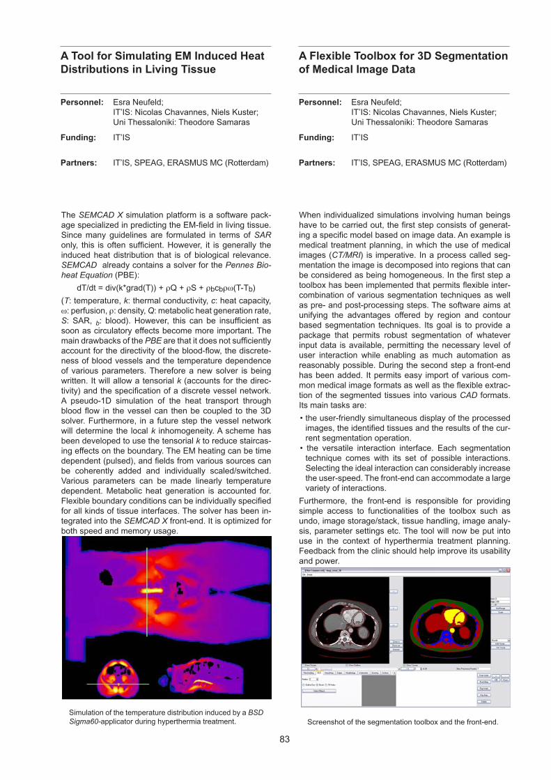
83
Personnel: Esra Neufeld; IT’IS: Nicolas Chavannes, Niels Kuster; Uni Thessaloniki: Theodore Samaras
Funding: IT’IS
Partners: IT’IS, SPEAG, ERASMUS MC (Rotterdam)
A Tool for Simulating EM Induced Heat Distributions in Living Tissue
Personnel: Esra Neufeld; IT’IS: Nicolas Chavannes, Niels Kuster; Uni Thessaloniki: Theodore Samaras
Funding: IT’IS
Partners: IT’IS, SPEAG, ERASMUS MC (Rotterdam)
A Flexible Toolbox for 3D Segmentation of Medical Image Data
The SEMCAD X simulation platform is a software pack-age specialized in predicting the EM-field in living tissue. Since many guidelines are formulated in terms of SAR only, this is often sufficient. However, it is generally the induced heat distribution that is of biological relevance. SEMCAD already contains a solver for the Pennes Bio-heat Equation (PBE):
dT/dt = div(k*grad(T)) + rQ + rS + rbcbrw(T-Tb)
(T: temperature, k: thermal conductivity, c: heat capacity, w: perfusion, r: density, Q: metabolic heat generation rate, S: SAR, b: blood). However, this can be insufficient as soon as circulatory effects become more important. The main drawbacks of the PBE are that it does not sufficiently account for the directivity of the blood-flow, the discrete-ness of blood vessels and the temperature dependence of various parameters. Therefore a new solver is being written. It will allow a tensorial k (accounts for the direc-tivity) and the specification of a discrete vessel network. A pseudo-1D simulation of the heat transport through blood flow in the vessel can then be coupled to the 3D solver. Furthermore, in a future step the vessel network will determine the local k inhomogeneity. A scheme has been developed to use the tensorial k to reduce staircas-ing effects on the boundary. The EM heating can be time dependent (pulsed), and fields from various sources can be coherently added and individually scaled/switched. Various parameters can be made linearly temperature dependent. Metabolic heat generation is accounted for. Flexible boundary conditions can be individually specified for all kinds of tissue interfaces. The solver has been in-tegrated into the SEMCAD X front-end. It is optimized for both speed and memory usage.
Simulation of the temperature distribution induced by a BSD Sigma60-applicator during hyperthermia treatment. Screenshot of the segmentation toolbox and the front-end.
When individualized simulations involving human beings have to be carried out, the first step consists of generat-ing a specific model based on image data. An example is medical treatment planning, in which the use of medical images (CT/MRI) is imperative. In a process called seg-mentation the image is decomposed into regions that can be considered as being homogeneous. In the first step a toolbox has been implemented that permits flexible inter-combination of various segmentation techniques as well as pre- and post-processing steps. The software aims at unifying the advantages offered by region and contour based segmentation techniques. Its goal is to provide a package that permits robust segmentation of whatever input data is available, permitting the necessary level of user interaction while enabling as much automation as reasonably possible. During the second step a front-end has been added. It permits easy import of various com-mon medical image formats as well as the flexible extrac-tion of the segmented tissues into various CAD formats. Its main tasks are:
• the user-friendly simultaneous display of the processed images, the identified tissues and the results of the cur-rent segmentation operation.
• the versatile interaction interface. Each segmentation technique comes with its set of possible interactions. Selecting the ideal interaction can considerably increase the user-speed. The front-end can accommodate a large variety of interactions.
Furthermore, the front-end is responsible for providing simple access to functionalities of the toolbox such as undo, image storage/stack, tissue handling, image analy-sis, parameter settings etc. The tool will now be put into use in the context of hyperthermia treatment planning. Feedback from the clinic should help improve its usability and power.
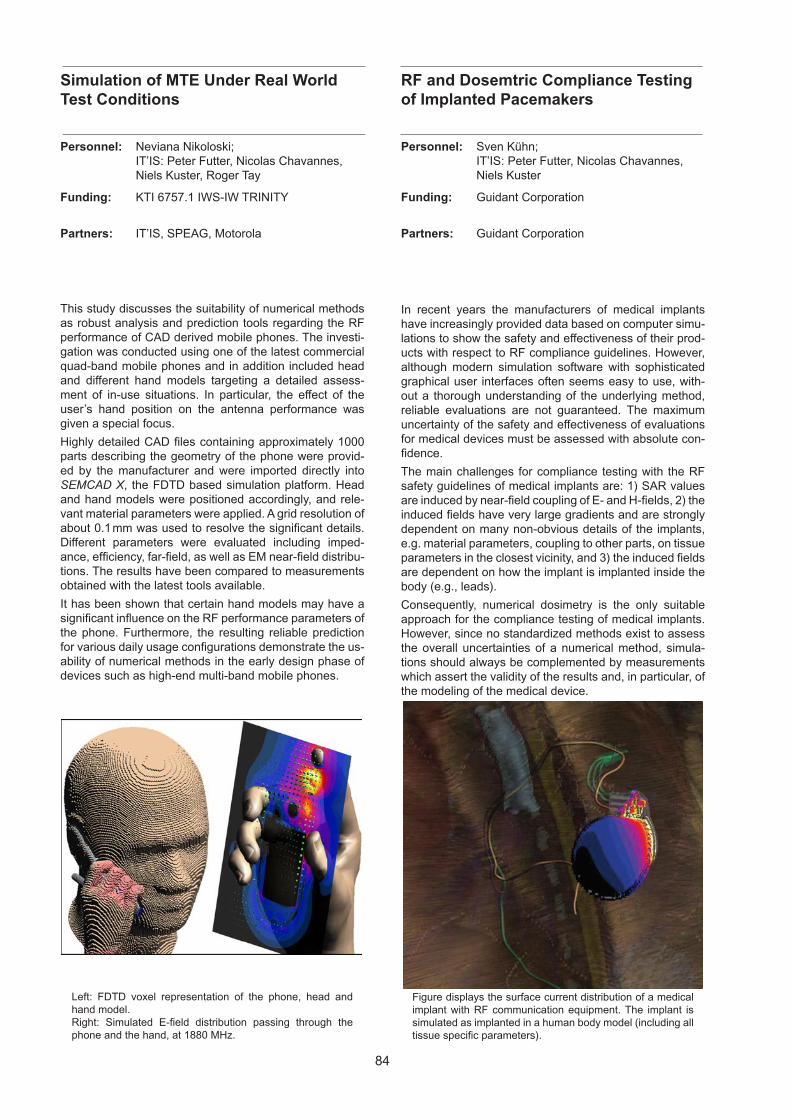
84
Personnel: Neviana Nikoloski; IT’IS: Peter Futter, Nicolas Chavannes, Niels Kuster, Roger Tay
Funding: KTI 6757.1 IWS-IW TRINITY
Partners: IT’IS, SPEAG, Motorola
Simulation of MTE Under Real World Test Conditions
Personnel: Sven Kühn; IT’IS: Peter Futter, Nicolas Chavannes, Niels Kuster
Funding: Guidant Corporation
Partners: Guidant Corporation
RF and Dosemtric Compliance Testing of Implanted Pacemakers
Left: FDTD voxel representation of the phone, head and hand model.Right: Simulated E-field distribution passing through the phone and the hand, at 1880 MHz.
This study discusses the suitability of numerical methods as robust analysis and prediction tools regarding the RF performance of CAD derived mobile phones. The investi-gation was conducted using one of the latest commercial quad-band mobile phones and in addition included head and different hand models targeting a detailed assess-ment of in-use situations. In particular, the effect of the user’s hand position on the antenna performance was given a special focus.
Highly detailed CAD files containing approximately 1000 parts describing the geometry of the phone were provid-ed by the manufacturer and were imported directly into SEMCAD X, the FDTD based simulation platform. Head and hand models were positioned accordingly, and rele-vant material parameters were applied. A grid resolution of about 0.1 mm was used to resolve the significant details. Different parameters were evaluated including imped-ance, efficiency, far-field, as well as EM near-field distribu-tions. The results have been compared to measurements obtained with the latest tools available.
It has been shown that certain hand models may have a significant influence on the RF performance parameters of the phone. Furthermore, the resulting reliable prediction for various daily usage configurations demonstrate the us-ability of numerical methods in the early design phase of devices such as high-end multi-band mobile phones.
In recent years the manufacturers of medical implants have increasingly provided data based on computer simu-lations to show the safety and effectiveness of their prod-ucts with respect to RF compliance guidelines. However, although modern simulation software with sophisticated graphical user interfaces often seems easy to use, with-out a thorough understanding of the underlying method, reliable evaluations are not guaranteed. The maximum uncertainty of the safety and effectiveness of evaluations for medical devices must be assessed with absolute con-fidence.
The main challenges for compliance testing with the RF safety guidelines of medical implants are: 1) SAR values are induced by near-field coupling of E- and H-fields, 2) the induced fields have very large gradients and are strongly dependent on many non-obvious details of the implants, e.g. material parameters, coupling to other parts, on tissue parameters in the closest vicinity, and 3) the induced fields are dependent on how the implant is implanted inside the body (e.g., leads).
Consequently, numerical dosimetry is the only suitable approach for the compliance testing of medical implants. However, since no standardized methods exist to assess the overall uncertainties of a numerical method, simula-tions should always be complemented by measurements which assert the validity of the results and, in particular, of the modeling of the medical device.
Figure displays the surface current distribution of a medical implant with RF communication equipment. The implant is simulated as implanted in a human body model (including all tissue specific parameters).
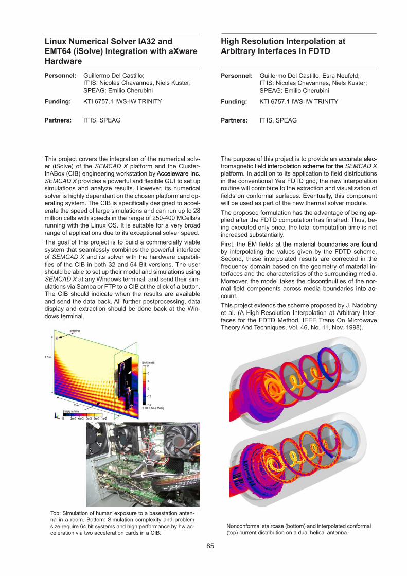
85
Personnel: Guillermo Del Castillo; IT’IS: Nicolas Chavannes, Niels Kuster; SPEAG: Emilio Cherubini
Funding: KTI 6757.1 IWS-IW TRINITY
Partners: IT’IS, SPEAG
Linux Numerical Solver IA32 and EMT64 (iSolve) Integration with aXware Hardware
Personnel: Guillermo Del Castillo, Esra Neufeld; IT’IS: Nicolas Chavannes, Niels Kuster; SPEAG: Emilio Cherubini
Funding: KTI 6757.1 IWS-IW TRINITY
Partners: IT’IS, SPEAG
High Resolution Interpolation atArbitrary Interfaces in FDTD
This project covers the integration of the numerical solv-er (iSolve) of the SEMCAD X platform and the Cluster-InABox (CIB) engineering workstation by Acceleware Inc.Acceleware Inc. SEMCAD X provides a powerful and flexible GUI to set up simulations and analyze results. However, its numerical solver is highly dependant on the chosen platform and op-erating system. The CIB is specifically designed to accel-erate the speed of large simulations and can run up to 28 million cells with speeds in the range of 250-400 MCells/s running with the Linux OS. It is suitable for a very broad range of applications due to its exceptional solver speed.
The goal of this project is to build a commercially viable system that seamlessly combines the powerful interface of SEMCAD X and its solver with the hardware capabili-ties of the CIB in both 32 and 64 Bit versions. The user should be able to set up their model and simulations using SEMCAD X at any Windows terminal, and send their sim-ulations via Samba or FTP to a CIB at the click of a button. The CIB should indicate when the results are available and send the data back. All further postprocessing, data display and extraction should be done back at the Win-dows terminal.
Top: Simulation of human exposure to a basestation anten-na in a room. Bottom: Simulation complexity and problem size require 64 bit systems and high performance by hw ac-celeration via two acceleration cards in a CIB.
The purpose of this project is to provide an accurate elec-elec-tromagnetic field interpolation scheme for theinterpolation scheme for the SEMCAD X platform. In addition to its application to field distributions in the conventional Yee FDTD grid, the new interpolation routine will contribute to the extraction and visualization of fields on conformal surfaces. Eventually, this component will be used as part of the new thermal solver module.
The proposed formulation has the advantage of being ap-plied after the FDTD computation has finished. Thus, be-ing executed only once, the total computation time is not increased substantially.
First, the EM fields at the material boundaries are foundat the material boundaries are foundare found by interpolating the values given by the FDTD scheme. Second, these interpolated results are corrected in the frequency domain based on the geometry of material in-terfaces and the characteristics of the surrounding media. Moreover, the model takes the discontinuities of the nor-mal field components across media boundaries into ac-into ac-count..
This project extends the scheme proposed by J. Nadobny et al. (A High-Resolution Interpolation at Arbitrary Inter-faces for the FDTD Method, IEEE Trans On Microwave Theory And Techniques, Vol. 46, No. 11, Nov. 1998).
Nonconformal staircase (bottom) and interpolated conformal (top) current distribution on a dual helical antenna.
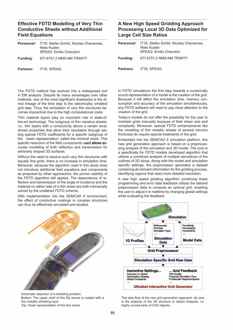
86
Effective FDTD Modelling of Very Thin Conductive Sheets without Additional Field Equations
Personnel: IT’IS: Stefan Schild, Nicolas Chavannes, Niels Kuster; SPEAG: Emilio Cherubini
Funding: KTI 6757.2 NMS-NM TRINITY
Partners: IT’IS, SPEAG
A New High Speed Gridding Approach Processing Local 3D Data Optimized for Large Cell Size Ratios
The FDTD method has evolved into a widespread tool in EM analysis. Despite its many advantages over other methods, one of the most significant drawbacks is the di-rect linkage of the time step to the (electrically) smallest grid step. Thus, the simulation of very thin structures be-comes impractical due to the high computational costs.
Thin material layers play an important role in state-of-the-art technology. The subgroup of thin resistive sheets, i.e., thin layers with a conductivity above a certain level, shows properties that allow their simulation through set-ting special FDTD coefficients for a specific subgroup of the mesh representation, called the minimal mesh. This specific reduction of the field components used allows ac-used allows ac-allows ac-curate modelling of both reflection and transmission for arbitrarily shaped 3D surfaces.
Without the need to resolve such very thin structures with equally fine grids, there is no increase in simulation time. Moreover, because the algorithm used in this study does not introduce additional field equations and components as proposed by other approaches, the proven stability of the FDTD algorithm still applies. The dependence of re-flection and transmission of the angle of incidence and the material on either side of a thin sheet are both intrinsically solved by the unaltered FDTD scheme.
With implementation into the SEMCAD X environment, the effect of conductive coatings in complex structures can thus be effectively simulated and studied.
Schematic depiction of a shielding problem.Bottom: The upper shell of this flip phone is coated with a thin metallic shielding layer.Top: Voxel representation of the thin sheet.
Personnel: IT’IS: Stefan Schild, Nicolas Chavannes, Niels Kuster; SPEAG: Emilio Cherubini
Funding: KTI 6757.2 NMS-NM TRINITY
Partners: IT’IS, SPEAG
In FDTD simulations the first step towards a numerically sound representation of a model is the creation of the grid. Because it will affect the simulation time, memory con-sumption and accuracy of the simulation simultaneously, any FDTD software will need to pay close attention to the creation of the grid.
Today‘s models do not offer the possibility for the user to maintain grids manually because of their sheer size and complexity. Moreover, special FDTD enhancements like the modeling of thin metallic sheets of several microns thickness do require special treatments of the grid.
Embedded into the SEMCAD X simulation platform, this new grid generation approach is based on a preproces-sing analysis of the simulation and 3D model. The core is a specifically for FDTD models developed algorithm that utilizes a combined analysis of multiple derivatives of the outlines of 2D slices. Along with the model and simulation specific settings, the preprocessor generates a dataset containing all relevant information for the gridding process, identifying regions that need more detailed resolution.
A new high speed gridding algorithm combining linear programming and error data feedback utilizes the tailored preprocessor data to compute an optimal grid, enabling the user to adjust it in realtime by changing global settings while evaluating the feedback.
The data flow of the new grid generation approach. Its core is the analysis of the 3D structure to detect hotspots, i.e. highly curved parts of CAD objects.
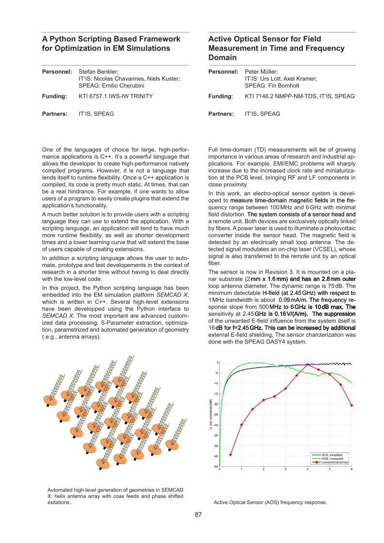
87
A Python Scripting Based Framework for Optimization in EM Simulations
Active Optical Sensor for FieldMeasurement in Time and Frequency Domain
One of the languages of choice for large, high-perfor-mance applications is C++. It’s a powerful language that allows the developer to create high-performance natively compiled programs. However, it is not a language that lends itself to runtime flexibility. Once a C++ application is compiled, its code is pretty much static. At times, that can be a real hindrance. For example, if one wants to allow users of a program to easily create plugins that extend the application’s functionality.
A much better solution is to provide users with a scripting language they can use to extend the application. With a scripting language, an application will tend to have much more runtime flexibility, as well as shorter development times and a lower learning curve that will extend the base of users capable of creating extensions.
In addition a scripting language allows the user to auto-mate, prototype and test developements in the context of research in a shorter time without having to deal directly with the low-level code.
In this project, the Python scripting language has been embedded into the EM simulation platform SEMCAD X, which is written in C++. Several high-level extensions have been developped using the Python interface to SEMCAD X. The most important are advanced custom-ized data processing, S-Parameter extraction, optimiza-tion, parametrized and automated generation of geometry ( e.g., antenna arrays).
Automated high-level generation of geometries in SEMCAD X: helix antenna array with coax feeds and phase shifted exitations.
Personnel: Stefan Benkler; IT’IS: Nicolas Chavannes, Niels Kuster; SPEAG: Emilio Cherubini
Funding: KTI 6757.1 IWS-IW TRINITY
Partners: IT’IS, SPEAG
Full time-domain (TD) measurements will be of growing importance in various areas of research and industrial ap-plications. For example, EMI/EMC problems will sharply increase due to the increased clock rate and miniaturiza-tion at the PCB level, bringing RF and LF components in close proximity.
In this work, an electro-optical sensor system is devel-oped to measure time-domain magnetic fields in the fre-measure time-domain magnetic fields in the fre-quency range between 100 MHz and 6 GHz with minimal field distortion. The system consists of a sensor head andThe system consists of a sensor head and a remote unit. Both devices are exclusively optically linked by fibers. A power laser is used to illuminate a photovoltaic converter inside the sensor head. The magnetic field is detected by an electrically small loop antenna. The de-tected signal modulates an on-chip laser (VCSEL), whose signal is also transferred to the remote unit by an optical fiber.
The sensor is now in Revision 3. It is mounted on a pla-nar substrate (2mm x 1.6mm) and has an 2.8mm outer mm x 1.6mm) and has an 2.8mm outermm x 1.6mm) and has an 2.8mm outer mm) and has an 2.8mm outermm) and has an 2.8 mm outer loop antenna diameter. The dynamic range is 75 dB. The minimum detectable H-field (at 2.45GHz) with respect toH-field (at 2.45 GHz) with respect to 1 MHz bandwidth is about 0.09mA/m. The frequency re- 0.09 mA/m. The frequency re-sponse slope from 500MHz to 6GHz is 10dB max. The MHz to 6GHz is 10dB max. TheMHz to 6GHz is 10dB max. The GHz is 10dB max. TheGHz is 10dB max. The dB max. ThedB max. The sensitivity at 2.45GHz is 0.16V/(A/m). The suppression GHz is 0.16V/(A/m). The suppressionGHz is 0.16V/(A/m). The suppression V/(A/m). The suppressionV/(A/m). The suppression of the unwanted E-field influence from the system itself is 16dB for f=2.45GHz. This can be increased by additional dB for f=2.45GHz. This can be increased by additionaldB for f=2.45GHz. This can be increased by additional GHz. This can be increased by additionalGHz. This can be increased by additional external E-field shielding. The sensor charcterization was done with the SPEAG DASY4 system.
Active Optical Sensor (AOS) frequency response.
Personnel: Peter Müller; IT’IS: Urs Lott, Axel Kramer; SPEAG: Fin Bomholt
Funding: KTI 7146.2 NMPP-NM-TDS, IT’IS, SPEAG
Partners: IT’IS, SPEAG
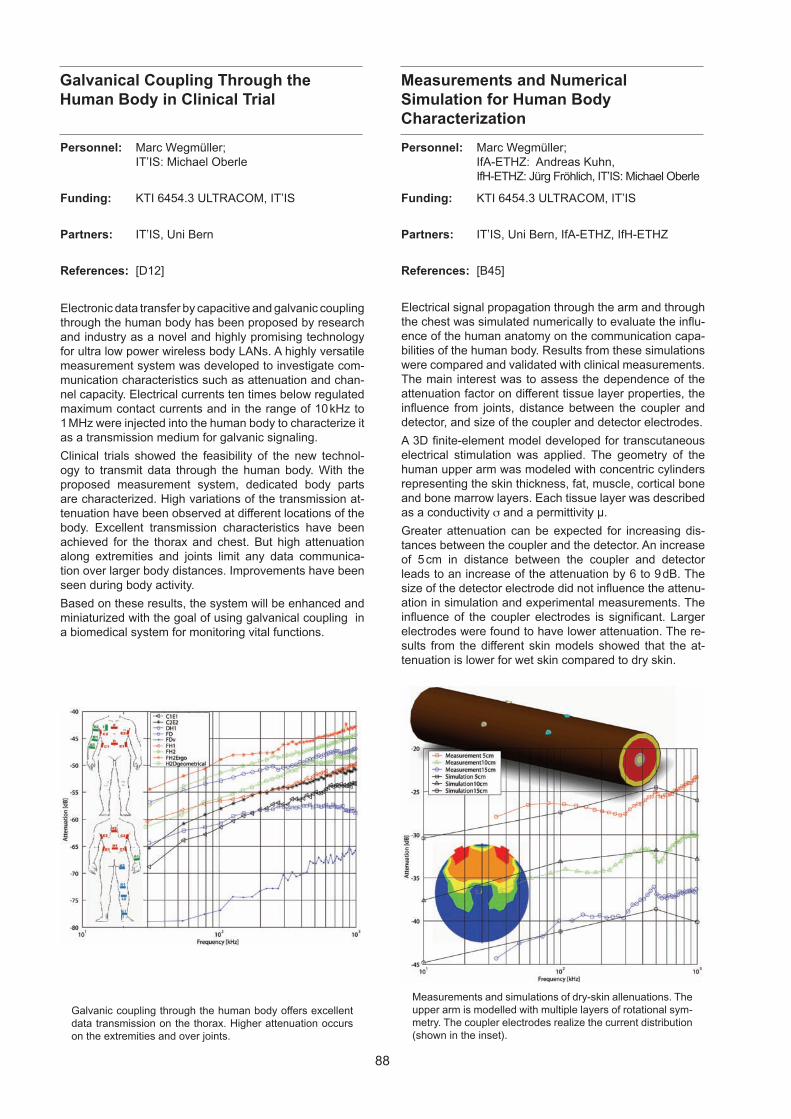
88
Galvanical Coupling Through theHuman Body in Clinical Trial
Measurements and NumericalSimulation for Human BodyCharacterization
Electronic data transfer by capacitive and galvanic coupling through the human body has been proposed by research and industry as a novel and highly promising technology for ultra low power wireless body LANs. A highly versatile measurement system was developed to investigate com-munication characteristics such as attenuation and chan-nel capacity. Electrical currents ten times below regulated maximum contact currents and in the range of 10 kHz to 1 MHz were injected into the human body to characterize it as a transmission medium for galvanic signaling.
Clinical trials showed the feasibility of the new technol-ogy to transmit data through the human body. With the proposed measurement system, dedicated body parts are characterized. High variations of the transmission at-tenuation have been observed at different locations of the body. Excellent transmission characteristics have been achieved for the thorax and chest. But high attenuation along extremities and joints limit any data communica-tion over larger body distances. Improvements have been seen during body activity.
Based on these results, the system will be enhanced and miniaturized with the goal of using galvanical coupling in a biomedical system for monitoring vital functions.
Galvanic coupling through the human body offers excellent data transmission on the thorax. Higher attenuation occurs on the extremities and over joints.
Personnel: Marc Wegmüller; IT’IS: Michael Oberle
Funding: KTI 6454.3 ULTRACOM, IT’IS
Partners: IT’IS, Uni Bern
References: [D12]
Electrical signal propagation through the arm and through the chest was simulated numerically to evaluate the influ-ence of the human anatomy on the communication capa-bilities of the human body. Results from these simulations were compared and validated with clinical measurements. The main interest was to assess the dependence of the attenuation factor on different tissue layer properties, the influence from joints, distance between the coupler and detector, and size of the coupler and detector electrodes.
A 3D finite-element model developed for transcutaneous electrical stimulation was applied. The geometry of the human upper arm was modeled with concentric cylinders representing the skin thickness, fat, muscle, cortical bone and bone marrow layers. Each tissue layer was described as a conductivity σ and a permittivity µ.
Greater attenuation can be expected for increasing dis-tances between the coupler and the detector. An increase of 5 cm in distance between the coupler and detector leads to an increase of the attenuation by 6 to 9 dB. The size of the detector electrode did not influence the attenu-ation in simulation and experimental measurements. The influence of the coupler electrodes is significant. Larger electrodes were found to have lower attenuation. The re-sults from the different skin models showed that the at-tenuation is lower for wet skin compared to dry skin.
Measurements and simulations of dry-skin allenuations. The upper arm is modelled with multiple layers of rotational sym-metry. The coupler electrodes realize the current distribution (shown in the inset).
Personnel: Marc Wegmüller; IfA-ETHZ: Andreas Kuhn, IfH-ETHZ: Jürg Fröhlich, IT’IS: Michael Oberle
Funding: KTI 6454.3 ULTRACOM, IT’IS
Partners: IT’IS, Uni Bern, IfA-ETHZ, IfH-ETHZ
References: [B45]
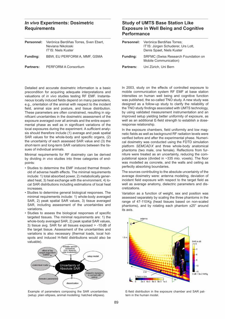
89
In vivo Experiments: Dosimetric Requirements
Study of UMTS Base Station Like Exposure in Well Being and CognitivePerformance
Detailed and accurate dosimetric information is a basic precondition for acquiring adequate interpretations and valuations of in vivo studies testing RF EMF. Instanta-neous locally induced fields depend on many parameters, e.g., orientation of the animal with respect to the incident field, animal size and posture, and tissue distribution. These parameters are often constrained, resulting in sig-nificant uncertainties in the dosimetric assessment of the exposure averaged over all animals and the entire experi-mental phase as well as in significant variations of the local exposures during the experiment. A sufficient analy-sis should therefore include (1) average and peak spatial SAR values for the whole-body and specific organs, (2) the uncertainty of each assessed SAR value and (3) the short-term and long-term SAR variations between the tis-sues of individual animals.
Minimal requirements for RF dosimetry can be derived by dividing in vivo studies into three categories of end-points:
• Studies to determine the EMF induced thermal thresh-old of adverse health effects. The minimal requirements include: 1) total absorbed power, 2) metabolically gener-ated heat, 3) heat exchange with the environment, 4) lo-cal SAR distributions including estimations of local heat increases.
• Studies to determine general biological responses. The minimal requirements include: 1) whole-body averaged SAR, 2) peak spatial SAR values, 3) tissue averaged SAR, including assessment of the uncertainties and variations.
• Studies to assess the biological responses of specific targeted tissues. The minimal requirements are: 1) the whole-body averaged SAR, 2) peak spatial SAR values, 3) tissue avg. SAR for all tissues exposed > -10 dB of the target tissue. Assessment of the uncertainties and variations is also necessary (thermal loads, local hot-spots and induced H-field distributions would also be valuable).
Example of parameters composing the SAR uncertainties (setup: plain ellipses, animal modelling: hatched ellipses).
Personnel: Verónica Berdiñas Torres, Sven Ebert, Neviana Nikoloski IT’IS: Niels Kuster
Funding: BBW, EU PERFORM A, MMF, GSMA
Partners: PERFORM A Consortium
In 2003, study on the effects of controlled exposure to mobile communication system RF EMF at base station intensities on human well being and cognitive function was published, the so-called TNO study. A new study was designed as a follow-up study to clarify the reliability of the TNO study findings associated with UMTS technology, by using validated measurement instrumentation and an improved setup yielding better uniformity of exposure, as well as an additional E-field strength to establish a dose-response relationship.
In the exposure chambers, field uniformity and low mag-netic fields as well as background RF radiation levels were verified before and after the experimental phase. Numeri-cal dosimetry was conducted using the FDTD simulation platform SEMCAD X and three whole-body anatomical phantoms (two male, one female). Reflections from fur-niture were treated as an uncertainty, reducing the com-putational space (divided in ~335 mio. voxels). The floor was modelled as concrete, and the walls and ceiling as perfectly absorbing boundaries.
The sources contributing to the absolute uncertainty of the average dosimetry were: antenna modeling, deviation of incident field exposure with respect to the target field as well as average anatomy, dielectric parameters and dis-cretizations.
Variation as a function of weight, sex and position was assessed separately by scaling the three phantoms in the range of 47-110 Kg (head tissues based on non-scaled phantoms), and by rotating each phantom ±25° around its axis.
E-field distribution in the exposure chamber and SAR pat-tern in the human model.
Personnel: Verónica Berdiñas Torres; IT’IS: Jürgen Schuderer, Urs Lott, Denis Spaet, Niels Kuster
Funding: SRFMC (Swiss Research Foundation on Mobile Communication)
Partners: Uni Zürich, Uni Bern
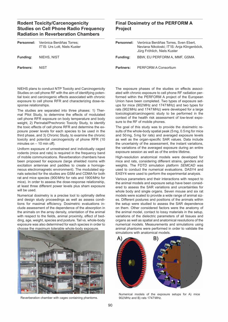
90
Rodent Toxicity/Carcenogenicity Studies on Cell Phone Radio FrequencyRadiation in Reverberation Chambers
Final Dosimetry of the PERFORM A Project
NIEHS plans to conduct NTP Toxicity and Carcinogenicity Studies on cell phone RF with the aim of identifying poten-tial toxic and carcinogenic effects associated with chronic exposure to cell phone RFR and characterizing dose-re-sponse relationships.
The studies are separated into three phases: 1) Ther-mal Pilot Study, to determine the effects of modulated cell phone RFR exposure on body temperature and body weight, 2) Perinatal/Prechronic Toxicity Study, to identify the toxic effects of cell phone RFR and determine the ex-posure power levels for each species to be used in the third phase, and 3) Chronic Study, to examine the chronic toxicity and potential carcinogenicity of phone RFR (10 minutes on – 10 min off).
Uniform exposure of unrestrained and individually caged rodents (mice and rats) is required in the frequency band of mobile communications. Reverberation chambers have been proposed for exposure (large shielded rooms with excitation antennae and paddles to create a homoge-neous electromagnetic environment). The modulated sig-nals selected for the studies are GSM and CDMA for both rat and mice species (900 MHz for rats and 1900 MHz for mice). In order to assess the dose-response relationship, at least three different power levels plus sham exposure will be used.
Numerical dosimetry is a precise tool to optimally define and design study proceedings as well as assess condi-tions for maximal efficiency. Dosimetric evaluations in-clude assessment of the dependence of the absorption in the animals on the array density, orientation of the animal with respect to the fields, animal proximity, effect of bed-ding, age, weight, species and posture. Tail vs. whole-body exposure was also determined for each species in order to choose the maximum tolerable whole-body exposure.
Reverberation chamber with cages containing phantoms.
Personnel: Verónica Berdiñas Torres; IT’IS: Urs Lott, Niels Kuster
Funding: NIEHS, NIST
Partners: NIST
The exposure phases of the studies on effects associ-ated with chronic exposure to cell phone RF radiation per-formed within the PERFORM A project of the European Union have been completed. Two types of exposure set-ups for mice (902 MHz and 1747 MHz) and two types for rats (902 MHz and 1747 MHz) were developed for a large toxicological/carcinogenic study to be performed in the context of the health risk assessment of low-level expo-sure to the RF of mobile phones.
The goal of this study was to provide the dosimetric re-sults of the whole-body spatial peak (5 mg, 0.5 mg for mice and 50 mg, 5 mg for rats) and averaged exposure levels as well as the organ-specific SAR values. Data include the uncertainty of the assessment, the instant variations, the variations of the averaged exposure during an entire exposure session as well as of the entire lifetime.
High-resolution anatomical models were developed for mice and rats, considering different strains, genders and weights. The FDTD simulation platform SEMCAD was used to conduct the numerical evaluations. DASY4 and EASY4 were used to perform the experimental analysis.
Various parameters and their interactions with respect to the animal models and exposure setup have been consid-ered to assess the SAR variations and uncertainties for whole body and single organs. Seven mouse and six rat models were scaled to provide a wide range of animal siz-es. Different postures and positions of the animals within the setup were studied to assess the SAR dependence on them. Other considered factors were the anatomy of the animal model, contact to lossy materials in the setup, variations of the dielectric parameters of all tissues and organs as well as spatial and anatomical resolutions of the numerical models. Measurements and simulations using animal phantoms were performed in order to validate the simulations with anatomical models.
Numerical models of the exposure setups for A) mice 902 MHz and B) rats 1747 MHz.
Personnel: Verónica Berdiñas Torres, Sven Ebert, Neviana Nikoloski; IT’IS: Anja Klingenböck, Jürg Fröhlich, Niels Kuster
Funding: BBW, EU PERFORM A, MMF, GSMA
Partners: PERFORM A Consortium
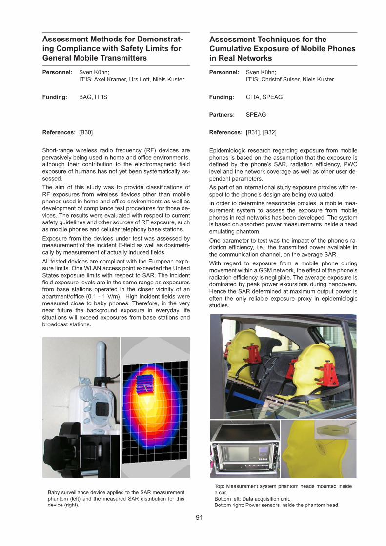
91
Assessment Methods for Demonstrat-ing Compliance with Safety Limits for General Mobile Transmitters
Assessment Techniques for the Cumulative Exposure of Mobile Phones in Real Networks
Epidemiologic research regarding exposure from mobile phones is based on the assumption that the exposure is defined by the phone’s SAR, radiation efficiency, PWC level and the network coverage as well as other user de-pendent parameters.
As part of an international study exposure proxies with re-spect to the phone’s design are being evaluated.
In order to determine reasonable proxies, a mobile mea-surement system to assess the exposure from mobile phones in real networks has been developed. The system is based on absorbed power measurements inside a head emulating phantom.
One parameter to test was the impact of the phone’s ra-diation efficiency, i.e., the transmitted power available in the communication channel, on the average SAR.
With regard to exposure from a mobile phone during movement within a GSM network, the effect of the phone’s radiation efficiency is negligible. The average exposure is dominated by peak power excursions during handovers. Hence the SAR determined at maximum output power is often the only reliable exposure proxy in epidemiologic studies.
Top: Measurement system phantom heads mounted inside a car.Bottom left: Data acquisition unit.Bottom right: Power sensors inside the phantom head.
Personnel: Sven Kühn; IT’IS: Christof Sulser, Niels Kuster
Funding: CTIA, SPEAG
Partners: SPEAG
References: [B31], [B32]
Short-range wireless radio frequency (RF) devices are pervasively being used in home and office environments, although their contribution to the electromagnetic field exposure of humans has not yet been systematically as-sessed.
The aim of this study was to provide classifications of RF exposures from wireless devices other than mobile phones used in home and office environments as well as development of compliance test procedures for those de-vices. The results were evaluated with respect to current safety guidelines and other sources of RF exposure, such as mobile phones and cellular telephony base stations.
Exposure from the devices under test was assessed by measurement of the incident E-field as well as dosimetri-cally by measurement of actually induced fields.
All tested devices are compliant with the European expo-sure limits. One WLAN access point exceeded the United States exposure limits with respect to SAR. The incident field exposure levels are in the same range as exposures from base stations operated in the closer vicinity of an apartment/office (0.1 - 1 V/m). High incident fields were measured close to baby phones. Therefore, in the very near future the background exposure in everyday life situations will exceed exposures from base stations and broadcast stations.
Baby surveillance device applied to the SAR measurement phantom (left) and the measured SAR distribution for this device (right).
Personnel: Sven Kühn; IT’IS: Axel Kramer, Urs Lott, Niels Kuster
Funding: BAG, IT`IS
References: [B30]
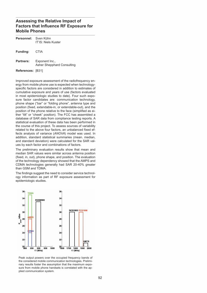
92
Personnel: Sven Kühn IT’IS: Niels Kuster
Funding: CTIA
Partners: Exponent Inc., Asher Shepphard Consulting
References: [B31]
Assessing the Relative Impact ofFactors that Influence RF Exposure forMobile Phones
Improved exposure assessment of the radiofrequency en-ergy from mobile phone use is expected when technology-specific factors are considered in addition to estimates of cumulative exposure and years of use (factors evaluated in most epidemiologic studies to date). Four such expo-sure factor candidates are: communication technology, phone shape (“bar” or “folding phone”, antenna type and position (fixed, extendable-in, or extendable-out), and the position of the phone relative to the face (simplified as ei-ther “tilt” or “cheek” position). The FCC has assembled a database of SAR data from compliance testing reports. A statistical evaluation of these data has been performed in the course of this project. To assess sources of variability related to the above four factors, an unbalanced fixed ef-fects analysis of variance (ANOVA) model was used. In addition, standard statistical summaries (mean. median, and standard deviation) were calculated for the SAR val-ues by each factor and combinations of factors.
The preliminary evaluation results show that mean and median SAR values were similar across antenna position (fixed, in, out), phone shape, and position. The evaluation of the technology dependency showed that the AMPS and CDMA technologies generally had SAR 20-40% greater than GSM and TDMA.
The findings suggest the need to consider service technol-ogy information as part of RF exposure assessment for epidemiologic studies.
Peak output powers over the occupied frequency bands of the considered mobile communication technologies. Prelimi-nary results foster the assumption that the maximum expo-sure from mobile phone handsets is correlated with the ap-plied communication system.

93
Education Program
Student Projects
Coordinator:
Norbert Felber

94
Introduction
Teaching microelectronics is one of the core activities of the Integrated Systems Laboratory. Shortly after the laboratory was founded in 1986, it started to offer projects in IC design to students. Probably as the first European university ETH financed the fabrication of student chips. This gave students the opportunity to carry out a VLSI design project from the specification to the test of their own silicon chips. Still today, the majority of student semester projects at IIS are in practical chip design, and many diploma projects include the realization of integrated circuits or the development of components as contribution to research ASICs. Since the first VLSI course offered by IIS, around 500 engineering students have had the chance of designing real silicon. During times of a prospering market, our students had all the chances of finding jobs in and outside Switzerland. More important, also during the periodic low-phases of the electronics industry, hardly any student special-ized in VLSI had problems to find an adequate job in less than a few months. Although basic microelectronics industry is rare in Switzerland, many other companies need knowledge on designing electronic circuits for the development of their products.
Education in MicroelectronicsDuring the first four semesters, students are motivated towards microelectronics by several PPS (Practicals, Projects, Seminars) (http://www.iis.ee.ethz.ch/stud_area/pps.en.html). In semester 5 and 6 the practical trainings (Fachpraktika, http://www.iis. ee.ethz.ch/stud_area/fachpraktika.en.html) offered by IIS aim at the same goal.
The three VLSI lectures from the 6th to the 8th semester illustrated in the figure on page 123 and described on page 125 build the main block in microelectronics education by the Integrated Systems Laboratory. Students who want to further deepen their experience in microelectronics often chose a diploma or master thesis in the framework of a research project of IIS as culmination of their education. Some then stay in these research fields for performing a PhD thesis.
ASIC Design Projects
Students who have decided to realize an integrated circuit will learn a professional de-sign flow using industrial CAD tools. The figure to the right shows a simplified view of all tools involved and of the task they are applied for during the work. The tools are the same as used in research and by our main industry partners; provid-ers and products are indicat-ed. The diversity of this design environment demonstrates the considerable effort our stu-dents have to provide just to master the tools. Besides their ‘handcraft’ they want to learn IC design, and to realize an often challenging and complex project. Despite the hard work with many traps and complica-tions, almost all chips finally work as intended.
During the 14 weeks of a se-mester project, the design stu-dents put ‘official’ 50% of their work load into the realization of the chip, mostly even con-siderably more. First-time-right digital ICs of industrial com-plexity level often result. This is only possible due to the sound VLSI education and an excel-lent support for design and test offered by the PhD students of our Laboratory and the Micro-electronics Design Center of the Department of Information Technology and Electrical En-gineering (see page 133 and http://dz.ee.ethz.ch).
Overview over the tool framework for IC design supported by the Microelectronics Design Center of the Department of Information Technology and Electrical Engineering. In the exer-cises to the VLSI lectures, the students practice to use these tools which they then intensely apply during the design projects.
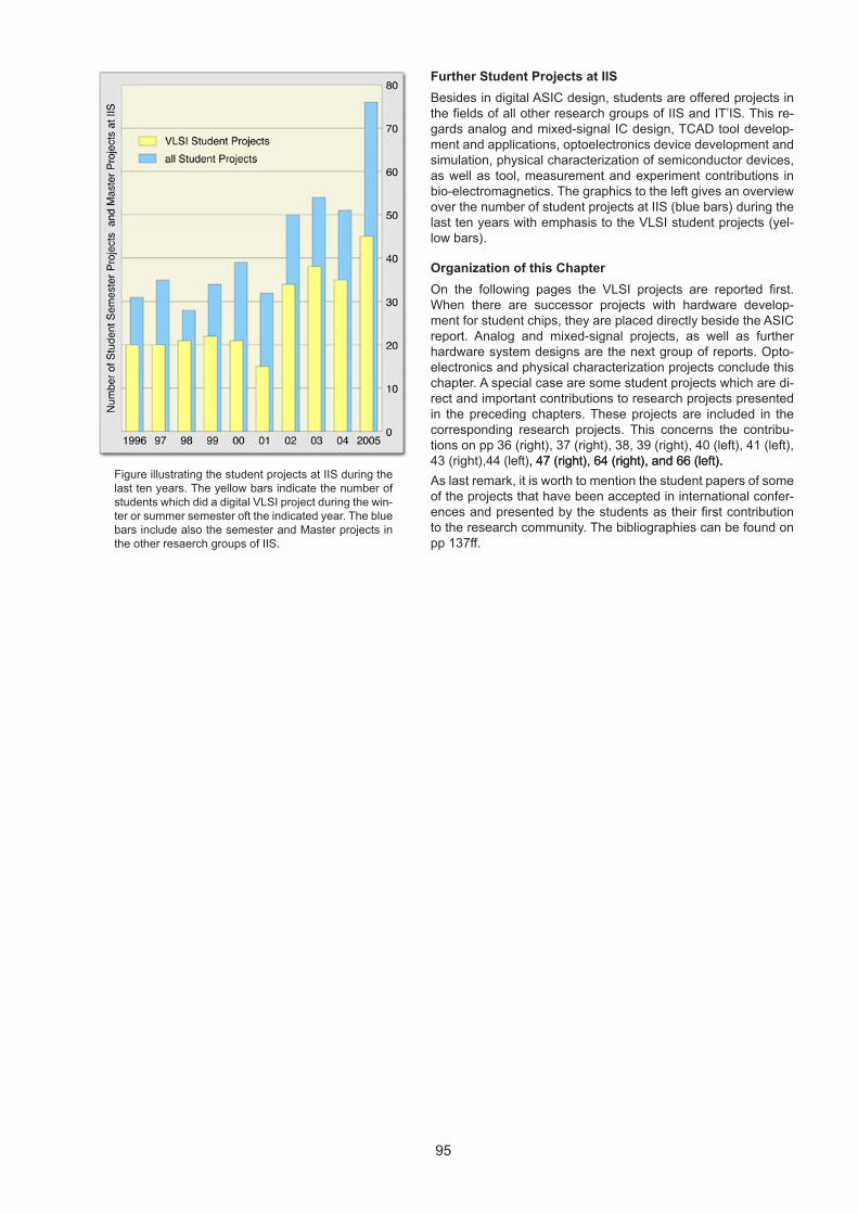
95
Further Student Projects at IIS
Besides in digital ASIC design, students are offered projects in the fields of all other research groups of IIS and IT’IS. This re-gards analog and mixed-signal IC design, TCAD tool develop-ment and applications, optoelectronics device development and simulation, physical characterization of semiconductor devices, as well as tool, measurement and experiment contributions in bio-electromagnetics. The graphics to the left gives an overview over the number of student projects at IIS (blue bars) during the last ten years with emphasis to the VLSI student projects (yel-low bars).
Organization of this Chapter
On the following pages the VLSI projects are reported first. When there are successor projects with hardware develop-ment for student chips, they are placed directly beside the ASIC report. Analog and mixed-signal projects, as well as further hardware system designs are the next group of reports. Opto-electronics and physical characterization projects conclude this chapter. A special case are some student projects which are di-rect and important contributions to research projects presented in the preceding chapters. These projects are included in the corresponding research projects. This concerns the contribu-tions on pp 36 (right), 37 (right), 38, 39 (right), 40 (left), 41 (left), 43 (right),44 (left), 47 (right), 64 (right), and 66 (left)., 47 (right), 64 (right), and 66 (left)..
As last remark, it is worth to mention the student papers of some of the projects that have been accepted in international confer-ences and presented by the students as their first contribution to the research community. The bibliographies can be found on pp 137ff.
Figure illustrating the student projects at IIS during the last ten years. The yellow bars indicate the number of students which did a digital VLSI project during the win-ter or summer semester oft the indicated year. The blue bars include also the semester and Master projects in the other resaerch groups of IIS.
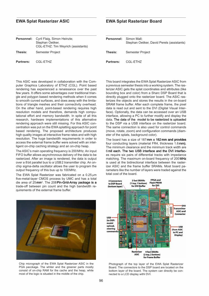
96
Personnel: Cyril Flaig, Simon Heinzle; Stephan Oetiker, CGL-ETHZ: Tim Weyrich (assistants)
Thesis: Semester Project
Partners: CGL-ETHZ
EWA Splat Rasterizer ASIC
Personnel: Simon Mall; Stephan Oetiker, David Perels (assistants)
Thesis: Semester Project
Partners: CGL-ETHZ
EWA Splat Rasterizer Board
This board integrates the EWA Splat Rasterizer ASIC from a previous semester thesis into a working system. The ras-terizer ASIC gets the splat coordinates and attributes (like bounding box and color) from a Sharc DSP Board that is directly plugged onto the rasterizer board. The ASIC ras-terizes the objects and stores the results in the on-board SRAM frame buffer. After each complete frame, the pixel data is read out and sent to the DVI (Digital Visual Inter-face). Optionally, the data can be accessed over an USB interface, allowing a PC to further modify and display the data. The data of the model to be rasterized is uploaded. The data of the model to be rasterized is uploaded to the DSP via a USB interface on the rasterizer board. The same connection is also used for control commands (move, rotate, zoom) and configuration commands (diam-eter of the splats, background color).
The board has a size of 187mm x 162mm and provides mm x 162mm and providesmm x 162mm and provides mm and providesmm and provides four conducting layers (material FR4, thickness 1.6mm). mm).mm). The minimum clearance and the minimum track width are 6mil each. The two USB interface and the DVI interfac- mil each. The two USB interface and the DVI interfac-mil each. The two USB interface and the DVI interfac-es require six pairs of differential tracks with impedance matching. The maximum on-board frequency of 200MHz MHzMHz is used at the bidirectional interface between the raster-izer ASIC and the frame buffer SRAMs. Most board pa-rameters like the number of layers were traded against the total cost of the board.
Photograph of the top layer of the EWA Splat Rasterizer Board. The connectors to the DSP board are located on the bottom layer of the board. The system can directly be con-nected to a LCD display withl DVI.
This ASIC was developed in collaboration with the Com-puter Graphics Laboratory of ETHZ (CGL). Point based rendering has experienced a renaissance over the past few years. It offers some advantages over traditional trian-gle and polygon based rendering methods when it comes to smooth curved surfaces, and does away with the limita-tions of triangle meshes and their connectivity overhead. On the other hand, point-based rendering requires high resolution models and therefore, demands high compu-tational effort and memory bandwidth. In spite of all this research, hardware implementations of this alternative rendering approach were still missing. For this ASIC con-centration was put on the EWA splatting approach for point based rendering. The proposed architecture produces high quality images at interactive frame rates and with high resolution. The huge bandwidth requirements in order to access the external frame buffer were solved with an intel-ligent on-chip caching strategy and an on-chip heap.
The ASIC’s main operating frequency is 200 MHz. An input FIFO buffer allows asynchronous delivery of the data to be rasterized. After an image is rendered, the data is output over a 8 bit parallel bus to a USB 2 transmitter chip. An on-chip sigma-delta oscillator allows the user to program the output frequency of this bus up to 100 MHz.
The EWA Splat Rasterizer was fabricated on a 0.25 mm five-metal-layer CMOS process by UMC and has a total die area of 25mm mmmm2. The 208Pin-Grid-Array package is a Pin-Grid-Array package is aPin-Grid-Array package is a trade-off between pin count and the high bandwidth re-quirements of the external frame buffer.
Chip micrograph of the EWA Splat Rasterizer ASIC in the PGA pacckage. The whiter and the greener parts mostly consist of on-chip RAM for the cache and the heap, while most of the logic is situated in the middle of the chip.
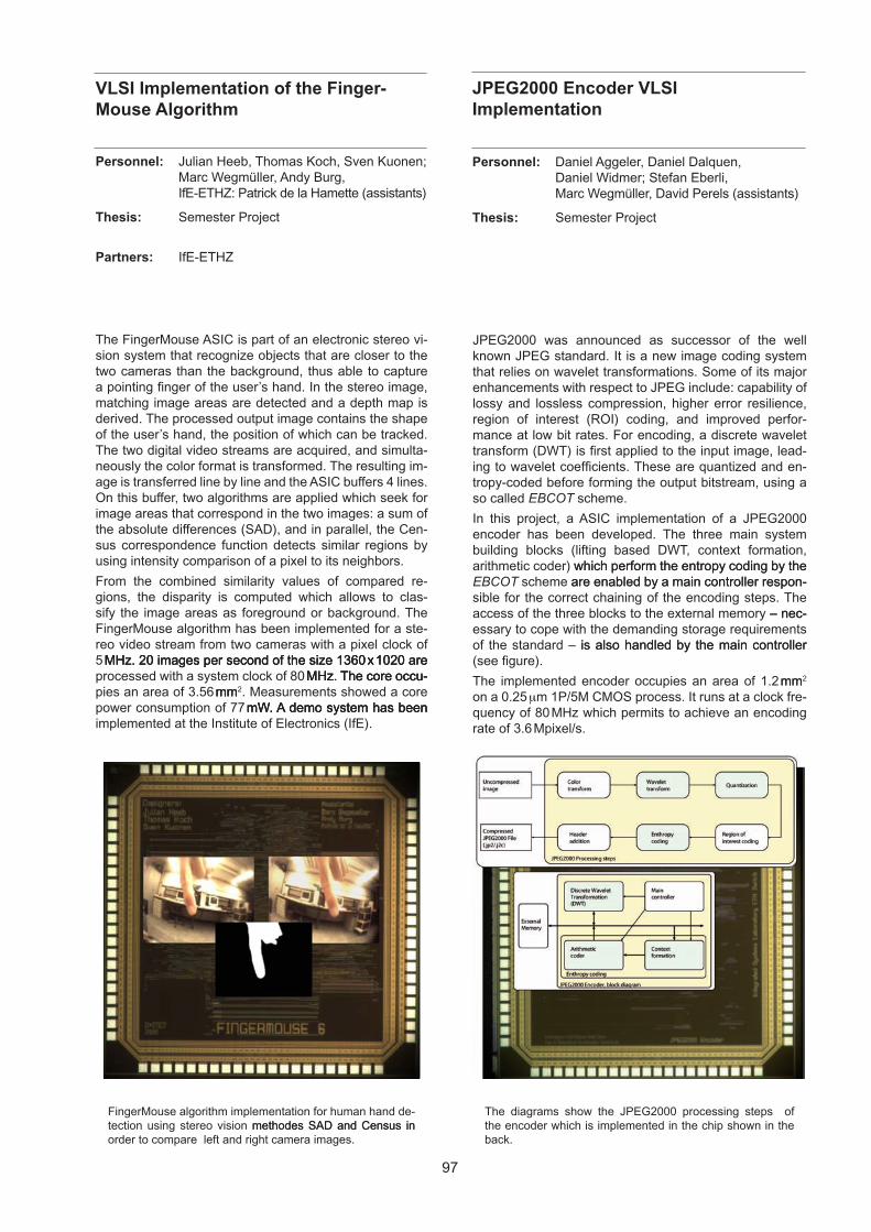
97
Personnel: Julian Heeb, Thomas Koch, Sven Kuonen; Marc Wegmüller, Andy Burg, IfE-ETHZ: Patrick de la Hamette (assistants)
Thesis: Semester Project
Partners: IfE-ETHZ
VLSI Implementation of the Finger-Mouse Algorithm
Personnel: Daniel Aggeler, Daniel Dalquen, Daniel Widmer; Stefan Eberli, Marc Wegmüller, David Perels (assistants)
Thesis: Semester Project
JPEG2000 Encoder VLSI Implementation
JPEG2000 was announced as successor of the well known JPEG standard. It is a new image coding system that relies on wavelet transformations. Some of its major enhancements with respect to JPEG include: capability of lossy and lossless compression, higher error resilience, region of interest (ROI) coding, and improved perfor-mance at low bit rates. For encoding, a discrete wavelet transform (DWT) is first applied to the input image, lead-ing to wavelet coefficients. These are quantized and en-tropy-coded before forming the output bitstream, using a so called EBCOT scheme.
In this project, a ASIC implementation of a JPEG2000 encoder has been developed. The three main system building blocks (lifting based DWT, context formation, arithmetic coder) which perform the entropy coding by thewhich perform the entropy coding by the EBCOT scheme are enabled by a main controller respon- are enabled by a main controller respon-sible for the correct chaining of the encoding steps. The access of the three blocks to the external memory – nec-– nec-essary to cope with the demanding storage requirements of the standard – is also handled by the main controller is also handled by the main controller (see figure).
The implemented encoder occupies an area of 1.2mm mm2
on a 0.25 mm 1P/5M CMOS process. It runs at a clock fre-quency of 80 MHz which permits to achieve an encoding rate of 3.6 Mpixel/s.
The diagrams show the JPEG2000 processing steps of the encoder which is implemented in the chip shown in the back.
The FingerMouse ASIC is part of an electronic stereo vi-sion system that recognize objects that are closer to the two cameras than the background, thus able to capture a pointing finger of the user’s hand. In the stereo image, matching image areas are detected and a depth map is derived. The processed output image contains the shape of the user’s hand, the position of which can be tracked. The two digital video streams are acquired, and simulta-neously the color format is transformed. The resulting im-age is transferred line by line and the ASIC buffers 4 lines. On this buffer, two algorithms are applied which seek for image areas that correspond in the two images: a sum of the absolute differences (SAD), and in parallel, the Cen-sus correspondence function detects similar regions by using intensity comparison of a pixel to its neighbors.
From the combined similarity values of compared re-gions, the disparity is computed which allows to clas-sify the image areas as foreground or background. The FingerMouse algorithm has been implemented for a ste-reo video stream from two cameras with a pixel clock of 5MHz. 20 images per second of the size 1360x1020 are MHz. 20 images per second of the size 1360x1020 areMHz. 20 images per second of the size 1360 x 1020 are processed with a system clock of 80MHz. The core occu- MHz. The core occu-MHz. The core occu-pies an area of 3.56mm mmmm2. Measurements showed a core power consumption of 77mW. A demo system has been mW. A demo system has beenmW. A demo system has been implemented at the Institute of Electronics (IfE).
FingerMouse algorithm implementation for human hand de-tection using stereo vision methodes SAD and Census inmethodes SAD and Census in order to compare left and right camera images.
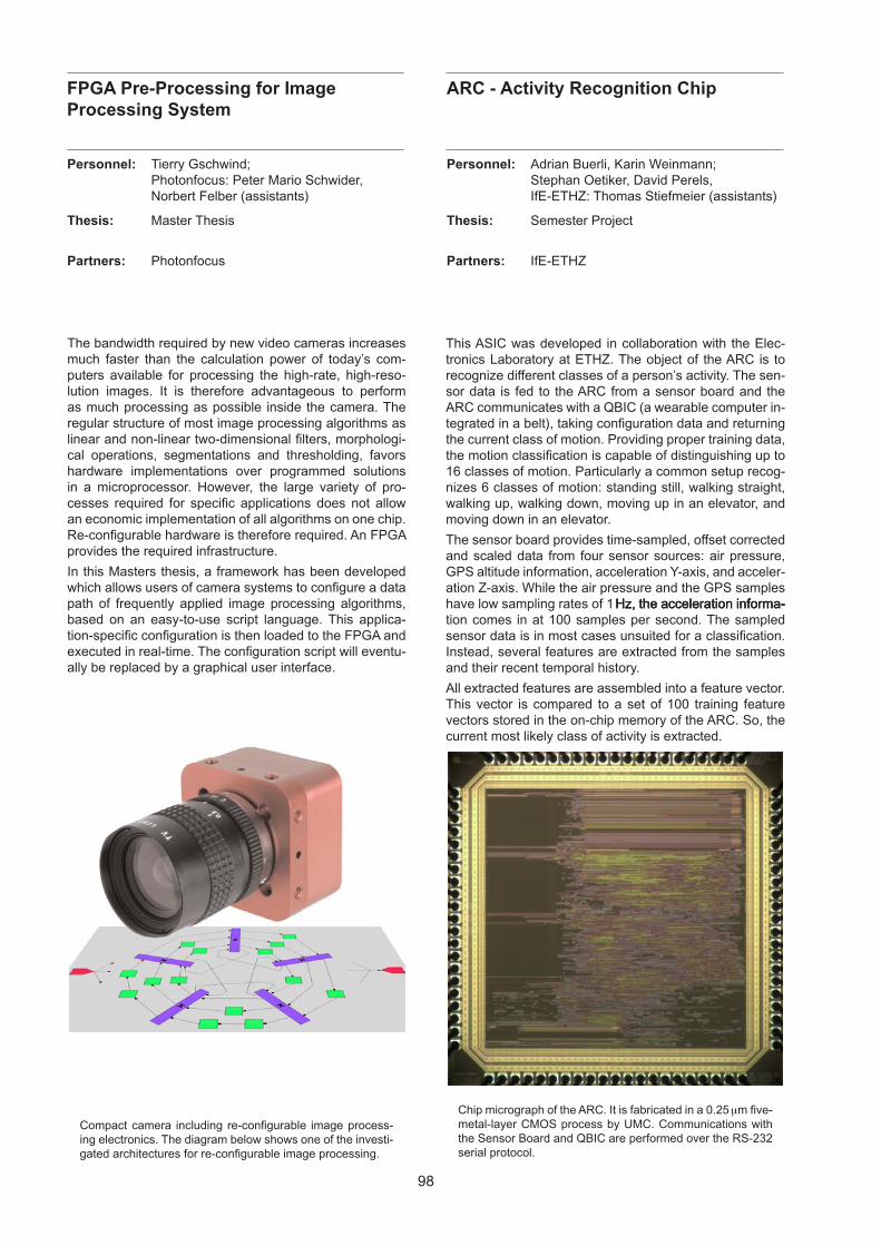
98
FPGA Pre-Processing for ImageProcessing System
Personnel: Adrian Buerli, Karin Weinmann; Stephan Oetiker, David Perels, IfE-ETHZ: Thomas Stiefmeier (assistants)
Thesis: Semester Project
Partners: IfE-ETHZ
ARC - Activity Recognition Chip
This ASIC was developed in collaboration with the Elec-tronics Laboratory at ETHZ. The object of the ARC is to recognize different classes of a person’s activity. The sen-sor data is fed to the ARC from a sensor board and the ARC communicates with a QBIC (a wearable computer in-tegrated in a belt), taking configuration data and returning the current class of motion. Providing proper training data, the motion classification is capable of distinguishing up to 16 classes of motion. Particularly a common setup recog-nizes 6 classes of motion: standing still, walking straight, walking up, walking down, moving up in an elevator, and moving down in an elevator.
The sensor board provides time-sampled, offset corrected and scaled data from four sensor sources: air pressure, GPS altitude information, acceleration Y-axis, and acceler-ation Z-axis. While the air pressure and the GPS samples have low sampling rates of 1Hz, the acceleration informa- Hz, the acceleration informa-Hz, the acceleration informa-tion comes in at 100 samples per second. The sampled sensor data is in most cases unsuited for a classification. Instead, several features are extracted from the samples and their recent temporal history.
All extracted features are assembled into a feature vector. This vector is compared to a set of 100 training feature vectors stored in the on-chip memory of the ARC. So, the current most likely class of activity is extracted.
Chip micrograph of the ARC. It is fabricated in a 0.25 mm five-metal-layer CMOS process by UMC. Communications with the Sensor Board and QBIC are performed over the RS-232 serial protocol.
The bandwidth required by new video cameras increases much faster than the calculation power of today’s com-puters available for processing the high-rate, high-reso-lution images. It is therefore advantageous to perform as much processing as possible inside the camera. The regular structure of most image processing algorithms as linear and non-linear two-dimensional filters, morphologi-cal operations, segmentations and thresholding, favors hardware implementations over programmed solutions in a microprocessor. However, the large variety of pro-cesses required for specific applications does not allow an economic implementation of all algorithms on one chip. Re-configurable hardware is therefore required. An FPGA provides the required infrastructure.
In this Masters thesis, a framework has been developed which allows users of camera systems to configure a data path of frequently applied image processing algorithms, based on an easy-to-use script language. This applica-tion-specific configuration is then loaded to the FPGA and executed in real-time. The configuration script will eventu-ally be replaced by a graphical user interface.
Compact camera including re-configurable image process-ing electronics. The diagram below shows one of the investi-gated architectures for re-configurable image processing.
Personnel: Tierry Gschwind; Photonfocus: Peter Mario Schwider, Norbert Felber (assistants)
Thesis: Master Thesis
Partners: Photonfocus
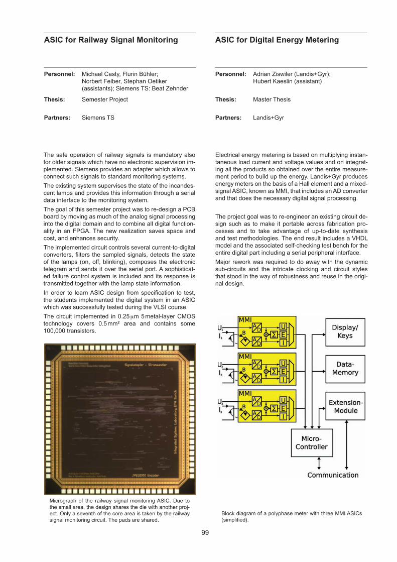
99
ASIC for Railway Signal Monitoring
Personnel: Adrian Ziswiler (Landis+Gyr); Hubert Kaeslin (assistant)
Thesis: Master Thesis
Partners: Landis+Gyr
ASIC for Digital Energy Metering
Electrical energy metering is based on multiplying instan-taneous load current and voltage values and on integrat-ing all the products so obtained over the entire measure-ment period to build up the energy. Landis+Gyr produces energy meters on the basis of a Hall element and a mixed-signal ASIC, known as MMI, that includes an AD converter and that does the necessary digital signal processing.
The project goal was to re-engineer an existing circuit de-sign such as to make it portable across fabrication pro-cesses and to take advantage of up-to-date synthesis and test methodologies. The end result includes a VHDL model and the associated self-checking test bench for the entire digital part including a serial peripheral interface.
Major rework was required to do away with the dynamic sub-circuits and the intricate clocking and circuit styles that stood in the way of robustness and reuse in the origi-nal design.
Block diagram of a polyphase meter with three MMI ASICs (simplified).
The safe operation of railway signals is mandatory also for older signals which have no electronic supervision im-plemented. Siemens provides an adapter which allows to connect such signals to standard monitoring systems.
The existing system supervises the state of the incandes-cent lamps and provides this information through a serial data interface to the monitoring system.
The goal of this semester project was to re-design a PCB board by moving as much of the analog signal processing into the digital domain and to combine all digital function-ality in an FPGA. The new realization saves space and cost, and enhances security.
The implemented circuit controls several current-to-digital converters, filters the sampled signals, detects the state of the lamps (on, off, blinking), composes the electronic telegram and sends it over the serial port. A sophisticat-ed failure control system is included and its response is transmitted together with the lamp state information.
In order to learn ASIC design from specification to test, the students implemented the digital system in an ASIC which was successfully tested during the VLSI course.
The circuit implemented in 0.25 mm 5 metal-layer CMOS technology covers 0.5 mm2 area and contains some 100,000 transistors.
Micrograph of the railway signal monitoring ASIC. Due to the small area, the design shares the die with another proj-ect. Only a seventh of the core area is taken by the railway signal monitoring circuit. The pads are shared.
Personnel: Michael Casty, Flurin Bühler; Norbert Felber, Stephan Oetiker (assistants); Siemens TS: Beat Zehnder
Thesis: Semester Project
Partners: Siemens TS
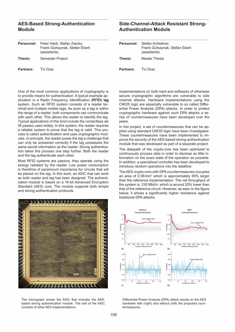
100
Personnel: Peter Haldi, Stefan Zwicky; Frank Gürkaynak, Stefan Eberli (assistants)
Thesis: Semester Project
Partners: TU Graz
AES-Based Strong-Authentication Module
Personnel: Stefan Achleitner; Frank Gürkaynak, Stefan Eberli (assistants)
Thesis: Master Thesis
Partners: TU Graz
Side-Channel-Attack Resistant Strong-Authentication Module
Implementations (in both hard and software) of otherwise secure cryptographic algorithms are vulnerable to side channel attacks. Hardware implementations using the CMOS logic are especially vulnerable to so called Differ-ential Power Analysis (DPA) attacks. In order to protect cryptographic hardware against such DPA attacks a se-ries of countermeasures have been developed over the years.
In this project, a set of countermeasures that can be ap-plied using standard CMOS logic have been investigated. These countermeasures have been implemented to im-prove the security of the AES-based strong-authentication module that was developed as part of a separate project.
The datapath of the crypto-core has been optimized to continuously process data in order to disclose as little in-formation on the exact state of the operation as possible. In addition, a specialized controller has been developed to introduce random operations into the dataflow.
The AES crypto-core with DPA countermeasures occupies an area of 0.58 mm2 which is approximately 65% larger than the reference implementation. The net throughput of the system is 230 Mbit/s which is around 20% lower than that of the reference circuit. However, as seen in the figure below, it shows a significantly higher resistance against traditional DPA attacks.
Differential Power Analysis (DPA) attack results on the AES hardware with (right) and without (left) the proposed coun-termeasures.
One of the most common applications of cryptography is to provide means for authentication. A typical example ap-plication is a Radio Frequency Identification (RFID) tag(RFID) tagtag system. Such an RFID system consists of a reader ter-minal and multiple mobile tags. As soon as a tag is within the range of a reader, both components can communicate with each other. This allows the reader to identify the tag. Typical applications of this kind include the contactless ski lift passes used widely. In this system, the reader requires a reliable system to prove that the tag is valid. This pro-cess is called authentication and uses cryptographic mod-ules. In principle, the reader poses the tag a challenge that can only be answered correctly if the tag possesses the same secret information as the reader. Strong authentica-tion takes this process one step further. Both the reader and the tag authenticate each other.
Most RFID systems are passive, they operate using the energy radiated by the reader. Low power consumption is therefore of paramount importance for circuits that will be placed on the tag. In this work, an ASIC that can work as both reader and tag has been designed. The authenti-cation module is based on a 16-bit Advanced Encryption Standard (AES) core. The module supports both simple and strong authentication protocols.
The micrograph shows the ASIC that includes the AES-based strong authentication module. The rest of the ASIC consists of other AES implementations.
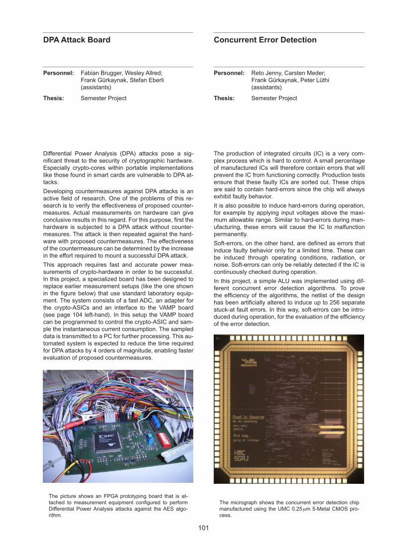
101
Personnel: Fabian Brugger, Wesley Allred; Frank Gürkaynak, Stefan Eberli (assistants)
Thesis: Semester Project
DPA Attack Board
Personnel: Reto Jenny, Carsten Meder; Frank Gürkaynak, Peter Lüthi (assistants)
Thesis: Semester Project
Concurrent Error Detection
The production of integrated circuits (IC) is a very com-plex process which is hard to control. A small percentage of manufactured ICs will therefore contain errors that will prevent the IC from functioning correctly. Production tests ensure that these faulty ICs are sorted out. These chips are said to contain hard-errors since the chip will always exhibit faulty behavior.
It is also possible to induce hard-errors during operation, for example by applying input voltages above the maxi-mum allowable range. Similar to hard-errors during man-ufacturing, these errors will cause the IC to malfunction permanently.
Soft-errors, on the other hand, are defined as errors that induce faulty behavior only for a limited time. These can be induced through operating conditions, radiation, or noise. Soft-errors can only be reliably detected if the IC is continuously checked during operation.
In this project, a simple ALU was implemented using dif-ferent concurrent error detection algorithms. To prove the efficiency of the algorithms, the netlist of the design has been artificially altered to induce up to 256 separate stuck-at fault errors. In this way, soft-errors can be intro-duced during operation, for the evaluation of the efficiency of the error detection.
The micrograph shows the concurrent error detection chip manufactured using the UMC 0.25 mm 5-Metal CMOS pro-cess.
Differential Power Analysis (DPA) attacks pose a sig-nificant threat to the security of cryptographic hardware. Especially crypto-cores within portable implementations like those found in smart cards are vulnerable to DPA at-tacks.
Developing countermeasures against DPA attacks is an active field of research. One of the problems of this re-search is to verify the effectiveness of proposed counter-measures. Actual measurements on hardware can give conclusive results in this regard. For this purpose, first the hardware is subjected to a DPA attack without counter-measures. The attack is then repeated against the hard-ware with proposed countermeasures. The effectiveness of the countermeasure can be determined by the increase in the effort required to mount a successful DPA attack.
This approach requires fast and accurate power mea-surements of crypto-hardware in order to be successful. In this project, a specialized board has been designed to replace earlier measurement setups (like the one shown in the figure below) that use standard laboratory equip-ment. The system consists of a fast ADC, an adapter for the crypto-ASICs and an interface to the VAMP board (see page 104 left-hand). In this setup the VAMP board can be programmed to control the crypto-ASIC and sam-ple the instantaneous current consumption. The sampled data is transmitted to a PC for further processing. This au-tomated system is expected to reduce the time required for DPA attacks by 4 orders of magnitude, enabling faster evaluation of proposed countermeasures.
The picture shows an FPGA prototyping board that is at-tached to measurement equipment configured to perform Differential Power Analysis attacks against the AES algo-rithm.
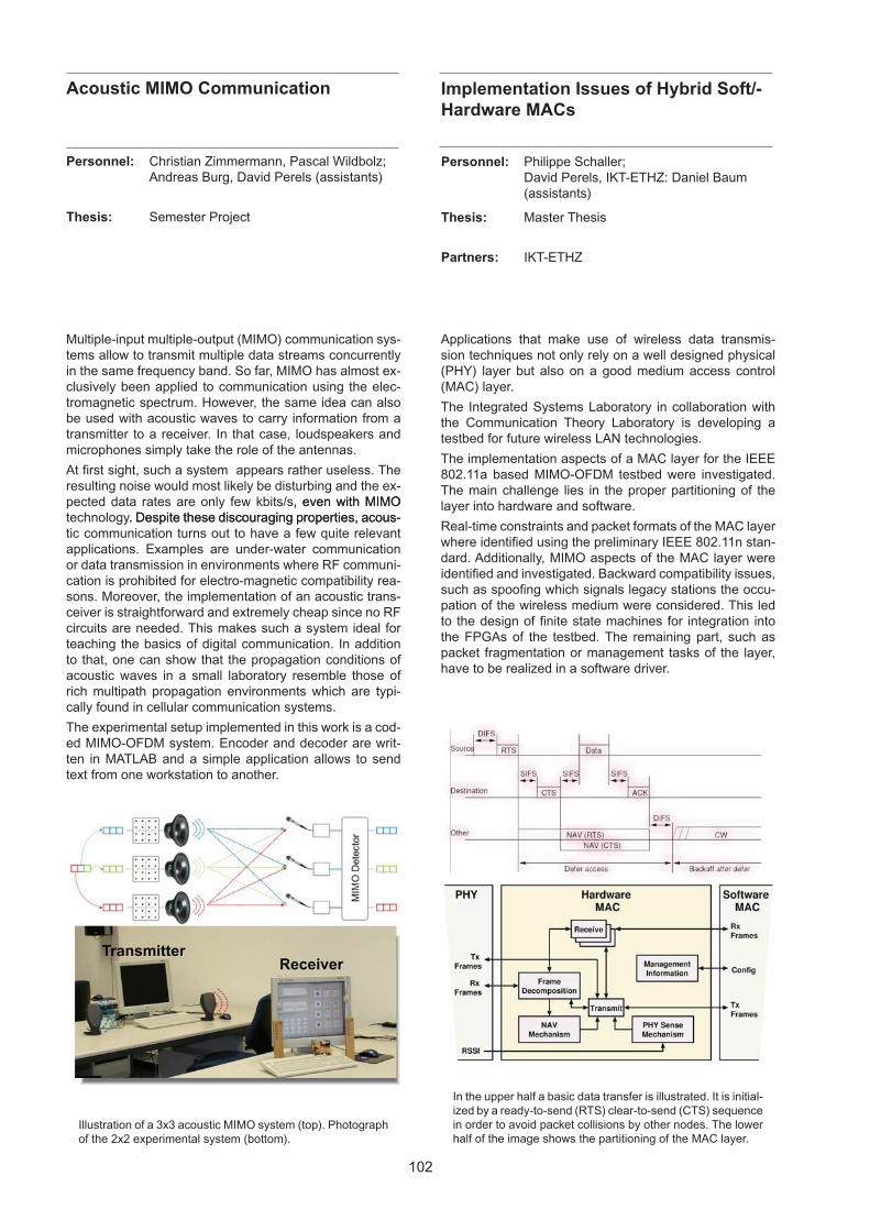
102
Personnel: Christian Zimmermann, Pascal Wildbolz; Andreas Burg, David Perels (assistants)
Thesis: Semester Project
Acoustic MIMO Communication
Personnel: Philippe Schaller; David Perels, IKT-ETHZ: Daniel Baum (assistants)
Thesis: Master Thesis
Partners: IKT-ETHZ
Implementation Issues of Hybrid Soft/-Hardware MACs
Applications that make use of wireless data transmis-sion techniques not only rely on a well designed physical (PHY) layer but also on a good medium access control (MAC) layer.
The Integrated Systems Laboratory in collaboration with the Communication Theory Laboratory is developing a testbed for future wireless LAN technologies.
The implementation aspects of a MAC layer for the IEEE 802.11a based MIMO-OFDM testbed were investigated. The main challenge lies in the proper partitioning of the layer into hardware and software.
Real-time constraints and packet formats of the MAC layer where identified using the preliminary IEEE 802.11n stan-dard. Additionally, MIMO aspects of the MAC layer were identified and investigated. Backward compatibility issues, such as spoofing which signals legacy stations the occu-pation of the wireless medium were considered. This led to the design of finite state machines for integration into the FPGAs of the testbed. The remaining part, such as packet fragmentation or management tasks of the layer, have to be realized in a software driver.
In the upper half a basic data transfer is illustrated. It is initial-ized by a ready-to-send (RTS) clear-to-send (CTS) sequence in order to avoid packet collisions by other nodes. The lower half of the image shows the partitioning of the MAC layer.
Multiple-input multiple-output (MIMO) communication sys-tems allow to transmit multiple data streams concurrently in the same frequency band. So far, MIMO has almost ex-clusively been applied to communication using the elec-tromagnetic spectrum. However, the same idea can also be used with acoustic waves to carry information from a transmitter to a receiver. In that case, loudspeakers and microphones simply take the role of the antennas.
At first sight, such a system appears rather useless. The resulting noise would most likely be disturbing and the ex-pected data rates are only few kbits/s, even with MIMO, even with MIMO technology. Despite these discouraging properties, acous-. Despite these discouraging properties, acous-tic communication turns out to have a few quite relevant applications. Examples are under-water communication or data transmission in environments where RF communi-cation is prohibited for electro-magnetic compatibility rea-sons. Moreover, the implementation of an acoustic trans-ceiver is straightforward and extremely cheap since no RF circuits are needed. This makes such a system ideal for teaching the basics of digital communication. In addition to that, one can show that the propagation conditions of acoustic waves in a small laboratory resemble those of rich multipath propagation environments which are typi-cally found in cellular communication systems.
The experimental setup implemented in this work is a cod-ed MIMO-OFDM system. Encoder and decoder are writ-ten in MATLAB and a simple application allows to send text from one workstation to another.
Illustration of a 3x3 acoustic MIMO system (top). Photograph of the 2x2 experimental system (bottom).
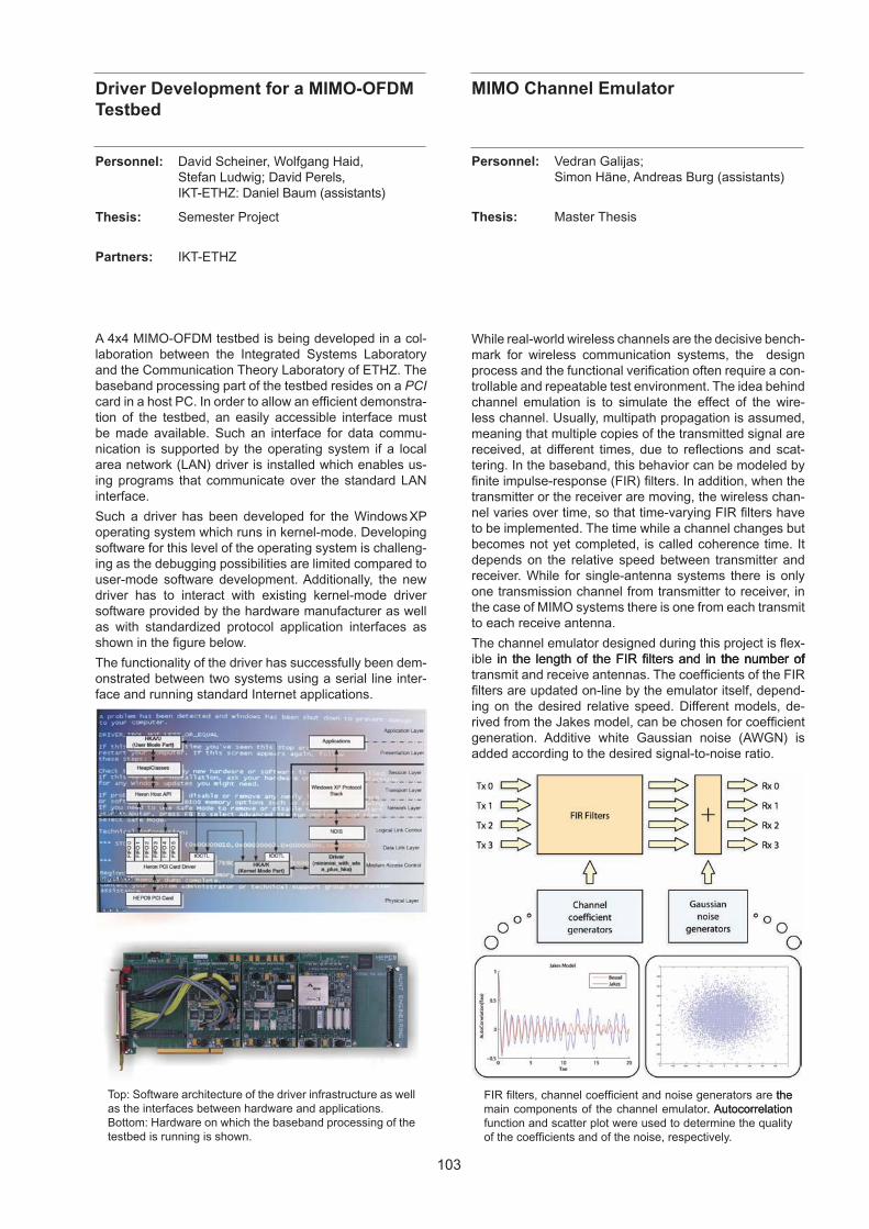
103
Personnel: David Scheiner, Wolfgang Haid, Stefan Ludwig; David Perels, IKT-ETHZ: Daniel Baum (assistants)
Thesis: Semester Project
Partners: IKT-ETHZ
Driver Development for a MIMO-OFDM Testbed
Personnel: Vedran Galijas; Simon Häne, Andreas Burg (assistants)
Thesis: Master Thesis
MIMO Channel Emulator
While real-world wireless channels are the decisive bench-mark for wireless communication systems, the design process and the functional verification often require a con-trollable and repeatable test environment. The idea behind channel emulation is to simulate the effect of the wire-less channel. Usually, multipath propagation is assumed, meaning that multiple copies of the transmitted signal are received, at different times, due to reflections and scat-tering. In the baseband, this behavior can be modeled by finite impulse-response (FIR) filters. In addition, when the transmitter or the receiver are moving, the wireless chan-nel varies over time, so that time-varying FIR filters have to be implemented. The time while a channel changes but becomes not yet completed, is called coherence time. It depends on the relative speed between transmitter and receiver. While for single-antenna systems there is only one transmission channel from transmitter to receiver, in the case of MIMO systems there is one from each transmit to each receive antenna.
The channel emulator designed during this project is flex-ible in the length of the FIR filters and in the number ofin the length of the FIR filters and in the number ofin the number of transmit and receive antennas. The coefficients of the FIR filters are updated on-line by the emulator itself, depend-ing on the desired relative speed. Different models, de-rived from the Jakes model, can be chosen for coefficient generation. Additive white Gaussian noise (AWGN) is added according to the desired signal-to-noise ratio.
FIR filters, channel coefficient and noise generators are thethe main components of the channel emulator. Autocorrelation. Autocorrelation function and scatter plot were used to determine the quality of the coefficients and of the noise, respectively.
A 4x4 MIMO-OFDM testbed is being developed in a col-laboration between the Integrated Systems Laboratory and the Communication Theory Laboratory of ETHZ. The baseband processing part of the testbed resides on a PCI card in a host PC. In order to allow an efficient demonstra-tion of the testbed, an easily accessible interface must be made available. Such an interface for data commu-nication is supported by the operating system if a local area network (LAN) driver is installed which enables us-ing programs that communicate over the standard LAN interface.
Such a driver has been developed for the Windows XP operating system which runs in kernel-mode. Developing software for this level of the operating system is challeng-ing as the debugging possibilities are limited compared to user-mode software development. Additionally, the new driver has to interact with existing kernel-mode driver software provided by the hardware manufacturer as well as with standardized protocol application interfaces as shown in the figure below.
The functionality of the driver has successfully been dem-onstrated between two systems using a serial line inter-face and running standard Internet applications.
Top: Software architecture of the driver infrastructure as well as the interfaces between hardware and applications. Bottom: Hardware on which the baseband processing of the testbed is running is shown.
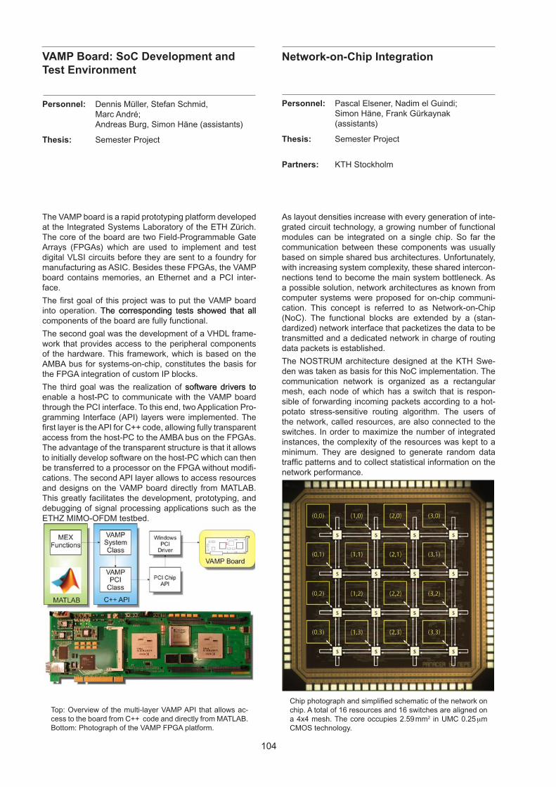
104
Personnel: Dennis Müller, Stefan Schmid, Marc André; Andreas Burg, Simon Häne (assistants)
Thesis: Semester Project
VAMP Board: SoC Development and Test Environment
Personnel: Pascal Elsener, Nadim el Guindi; Simon Häne, Frank Gürkaynak (assistants)
Thesis: Semester Project
Partners: KTH Stockholm
Network-on-Chip Integration
As layout densities increase with every generation of inte-grated circuit technology, a growing number of functional modules can be integrated on a single chip. So far the communication between these components was usually based on simple shared bus architectures. Unfortunately, with increasing system complexity, these shared intercon-nections tend to become the main system bottleneck. As a possible solution, network architectures as known from computer systems were proposed for on-chip communi-cation. This concept is referred to as Network-on-Chip (NoC). The functional blocks are extended by a (stan-dardized) network interface that packetizes the data to be transmitted and a dedicated network in charge of routing data packets is established.
The NOSTRUM architecture designed at the KTH Swe-den was taken as basis for this NoC implementation. The communication network is organized as a rectangular mesh, each node of which has a switch that is respon-sible of forwarding incoming packets according to a hot-potato stress-sensitive routing algorithm. The users of the network, called resources, are also connected to the switches. In order to maximize the number of integrated instances, the complexity of the resources was kept to a minimum. They are designed to generate random data traffic patterns and to collect statistical information on the network performance.
Chip photograph and simplified schematic of the network on chip. A total of 16 resources and 16 switches are aligned on a 4x4 mesh. The core occupies 2.59 mm2 in UMC 0.25 mm CMOS technology.
The VAMP board is a rapid prototyping platform developed at the Integrated Systems Laboratory of the ETH Zürich. The core of the board are two Field-Programmable Gate Arrays (FPGAs) which are used to implement and test digital VLSI circuits before they are sent to a foundry for manufacturing as ASIC. Besides these FPGAs, the VAMP board contains memories, an Ethernet and a PCI inter-face.
The first goal of this project was to put the VAMP board into operation. The corresponding tests showed that allThe corresponding tests showed that all components of the board are fully functional.
The second goal was the development of a VHDL frame-work that provides access to the peripheral components of the hardware. This framework, which is based on the AMBA bus for systems-on-chip, constitutes the basis for the FPGA integration of custom IP blocks.
The third goal was the realization of software drivers tosoftware drivers to enable a host-PC to communicate with the VAMP board through the PCI interface. To this end, two Application Pro-gramming Interface (API) layers were implemented. The first layer is the API for C++ code, allowing fully transparent access from the host-PC to the AMBA bus on the FPGAs. The advantage of the transparent structure is that it allows to initially develop software on the host-PC which can then be transferred to a processor on the FPGA without modifi-cations. The second API layer allows to access resources and designs on the VAMP board directly from MATLAB. This greatly facilitates the development, prototyping, and debugging of signal processing applications such as the ETHZ MIMO-OFDM testbed.
Top: Overview of the multi-layer VAMP API that allows ac-cess to the board from C++ code and directly from MATLAB. Bottom: Photograph of the VAMP FPGA platform.
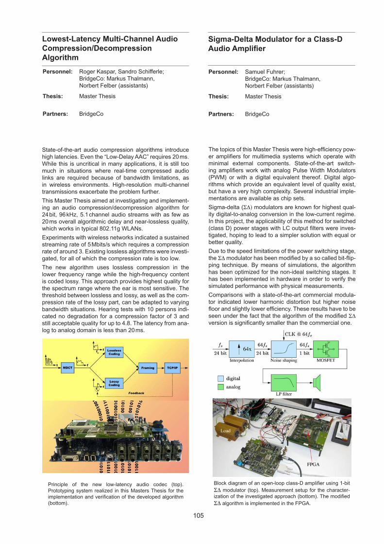
105
Lowest-Latency Multi-Channel Audio Compression/DecompressionAlgorithm
Sigma-Delta Modulator for a Class-D Audio Amplifier
State-of-the-art audio compression algorithms introduce high latencies. Even the “Low-Delay AAC” requires 20 ms. While this is uncritical in many applications, it is still too much in situations where real-time compressed audio links are required because of bandwidth limitations, as in wireless environments. High-resolution multi-channel transmissions exacerbate the problem further.
This Master Thesis aimed at investigating and implement-ing an audio compression/decompression algorithm for 24 bit, 96 kHz, 5.1 channel audio streams with as few as 20 ms overall algorithmic delay and near-lossless quality, which works in typical 802.11g WLANs.
Experiments with wireless networks indicated a sustained streaming rate of 5 Mbits/s which requires a compression rate of around 3. Existing lossless algorithms were investi-gated, for all of which the compression rate is too low.
The new algorithm uses lossless compression in the lower frequency range while the high-frequency content is coded lossy. This approach provides highest quality for the spectrum range where the ear is most sensitive. The threshold between lossless and lossy, as well as the com-pression rate of the lossy part, can be adapted to varying bandwidth situations. Hearing tests with 10 persons indi-cated no degradation for a compression factor of 3 and still acceptable quality for up to 4.8. The latency from ana-log to analog domain is less than 20 ms.
Principle of the new low-latency audio codec (top). Prototyping system realized in this Masters Thesis for the implementation and verification of the developed algorithm (bottom).
Personnel: Roger Kaspar, Sandro Schifferle; BridgeCo: Markus Thalmann, Norbert Felber (assistants)
Thesis: Master Thesis
Partners: BridgeCo
The topics of this Master Thesis were high-efficiency pow-er amplifiers for multimedia systems which operate with minimal external components. State-of-the-art switch-ing amplifiers work with analog Pulse Width Modulators (PWM) or with a digital equivalent thereof. Digital algo-rithms which provide an equivalent level of quality exist, but have a very high complexity. Several industrial imple-mentations are available as chip sets.
Sigma-delta (SD) modulators are known for highest qual-ity digital-to-analog conversion in the low-current regime. In this project, the applicability of this method for switched (class D) power stages with LC output filters were inves-tigated, hoping to lead to a simpler solution with equal or better quality.
Due to the speed limitations of the power switching stage, the SD modulator has been modified by a so called bit-flip-ping technique. By means of simulations, the algorithm has been optimized for the non-ideal switching stages. It has been implemented in hardware in order to verify the simulated performance with physical measurements.
Comparisons with a state-of-the-art commercial modula-tor indicated lower harmonic distortion but higher noise floor and slightly lower efficiency. These results have to be seen under the fact that the algorithm of the modified SD version is significantly smaller than the commercial one.
Block diagram of an open-loop class-D amplifier using 1-bit SD modulator (top). Measurement setup for the character-ization of the investigated approach (bottom). The modified SD algorithm is implemented in the FPGA.
Personnel: Samuel Fuhrer; BridgeCo: Markus Thalmann, Norbert Felber (assistants)
Thesis: Master Thesis
Partners: BridgeCo
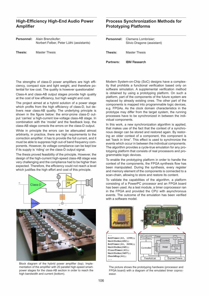
106
High-Efficiency High-End Audio Power Amplifier
Personnel: Clemens Lombrisier; Silvio Dragone (assistant)
Thesis: Master Thesis
Partners: IBM ResearchIBM Research
Process Synchronization Methods for Prototyping Platforms
The strengths of class-D power amplifiers are high effi-ciency, compact size and light weight, and therefore po-tential for low cost. The quality is however questionable!
Class-A and class-AB output stages provide high quality at the cost of low efficiency, but high weight and cost.
The project aimed at a hybrid solution of a power stage which profits from the high efficiency of class-D, but de-livers near class-AB quality. The underlying principle is shown in the figure below: the error-prone class-D out-put ‘carries’ a high-current low-voltage class-AB stage. In combination with the ‘model’ and the feedback loop, the class-AB stage corrects the errors on the class-D output.
While in principle the errors can be attenuated almost arbitrarily, in practice, there are high requirements to the correction amplifier: it has to provide the full current, and it must be able to suppress high out-of band frequency com-ponents. However, its voltage compliance can be kept low if its supply is ‘riding’ on the class-D output signal.
The thesis proved feasibility of the principle. However, the design of the high-current high-speed class-AB stage was very challenging and the compliance had to be higher than expected. Therefore, the efficiency could not reach a level which justifies the high effort and cost of this principle.
Block diagram of the hybrid power amplifier (top). Imple-mentation of the amplifier with 20 parallel high-speed smart-power stages for the class-AB section in order to reach the high bandwidth and current (bottom).
Personnel: Alain Brenzikofer; Norbert Felber, Peter Lüthi (assistants)
Thesis: Master Thesis
Modern System-on-Chip (SoC) designs have a complex-ity that prohibits a functional verification based only on software simulation. A supplemental verification method is obtained by using a prototyping platform. On such a platform, part of the components of the future system are replaced by already existing ones. The other part of the components is mapped into programmable logic devices, e.g. FPGAs. As the clock domain characteristics in the prototype may differ from the target system, the running processes have to be synchronized in between the indi-vidual components.
In this work, a new synchronization algorithm is applied, that makes use of the fact that the context of a synchro-nous design can be stored and restored again. By restor-ing an older context of a component, this component is set “back in time”. This effect is used to synchronize the events which occur in between the individual components. The algorithm provides a cycle-true emulation for any pro-totyping platform that consists of real processors and pro-grammable logic devices.
To enable the prototyping platform in order to handle the context of the components, the FPGA synthesis flow has been manipulated. During the synthesis, every register and memory element of the components is connected to a scan-chain, allowing to store and restore its content.
To validate the capabilities of the algorithm, a platform consisting of a PowerPC processor and an FPGA board has been used. As a test module, a timer coprocessor ran in the FPGA and provided the CPU with asynchronous events. The outcome of the emulation has been verified with a software model.
The picture shows the prototyping hardware (processor and FPGA board) with a diagram of the emulated timer coproc-essor.
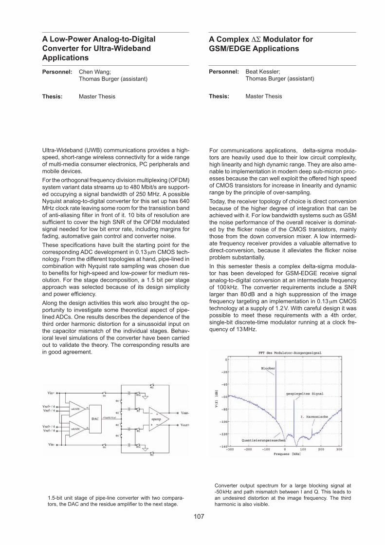
107
Personnel: Chen Wang; Thomas Burger (assistant)
Thesis: Master Thesis
A Low-Power Analog-to-DigitalConverter for Ultra-WidebandApplications
Personnel: Beat Kessler; Thomas Burger (assistant)
Thesis: Master Thesis
A Complex DS Modulator for GSM/EDGE Applications
Ultra-Wideband (UWB) communications provides a high-speed, short-range wireless connectivity for a wide range of multi-media consumer electronics, PC peripherals and mobile devices.
For the orthogonal frequency division multiplexing (OFDM) system variant data streams up to 480 Mbit/s are support-ed occupying a signal bandwidth of 250 MHz. A possible Nyquist analog-to-digital converter for this set up has 640 MHz clock rate leaving some room for the transistion band of anti-aliasing filter in front of it. 10 bits of resolution are sufficient to cover the high SNR of the OFDM modulated signal needed for low bit error rate, including margins for fading, automative gain control and converter noise.
These specifications have built the starting point for the corresponding ADC development in 0.13 mm CMOS tech-nology. From the different topologies at hand, pipe-lined in combination with Nyquist rate sampling was chosen due to benefits for high-speed and low-power for medium res-olution. For the stage decomposition, a 1.5 bit per stage approach was selected because of its design simplicity and power efficiency.
Along the design activities this work also brought the op-portunity to investigate some theoretical aspect of pipe-lined ADCs. One results describes the dependence of the third order harmonic distortion for a sinussoidal input on the capacitor mismatch of the individual stages. Behav-ioral level simulations of the converter have been carried out to validate the theory. The corresponding results are in good agreement.
1.5-bit unit stage of pipe-line converter with two compara-tors, the DAC and the residue amplifier to the next stage.
For communications applications, delta-sigma modula-tors are heavily used due to their low circuit complexity, high linearity and high dynamic range. They are also ame-nable to implementation in modern deep sub-micron proc-esses because the can well exploit the offered high speed of CMOS transistors for increase in linearity and dynamic range by the principle of over-sampling.
Today, the receiver topology of choice is direct conversion because of the higher degree of integration that can be achieved with it. For low bandwidth systems such as GSM the noise performance of the overall receiver is dominat-ed by the flicker noise of the CMOS transistors, mainly those from the down conversion mixer. A low intermedi-ate frequency receiver provides a valuable alternative to direct-conversion, because it alleviates the flicker noise problem substantially.
In this semester thesis a complex delta-sigma modula-tor has been developed for GSM-EDGE receive signal analog-to-digital conversion at an intermediate frequency of 100 kHz. The converter requirements include a SNR larger than 80 dB and a high suppression of the image frequency targeting an implementation in 0.13 mm CMOS technology at a supply of 1.2 V. With careful design it was possible to meet these requirements with a 4th order, single-bit discrete-time modulator running at a clock fre-quency of 13 MHz.
Converter output spectrum for a large blocking signal at -50 kHz and path mismatch between I and Q. This leads to an undesired distortion at the image frequency. The third harmonic is also visible.
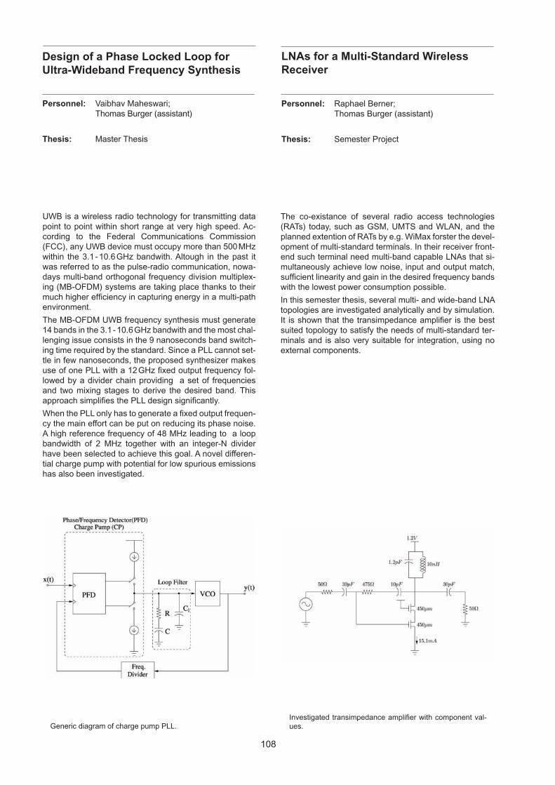
108
Personnel: Raphael Berner; Thomas Burger (assistant)
Thesis: Semester Project
LNAs for a Multi-Standard Wireless Receiver
Personnel: Vaibhav Maheswari; Thomas Burger (assistant)
Thesis: Master Thesis
Design of a Phase Locked Loop for Ultra-Wideband Frequency Synthesis
The co-existance of several radio access technologies (RATs) today, such as GSM, UMTS and WLAN, and the planned extention of RATs by e.g. WiMax forster the devel-opment of multi-standard terminals. In their receiver front-end such terminal need multi-band capable LNAs that si-multaneously achieve low noise, input and output match, sufficient linearity and gain in the desired frequency bands with the lowest power consumption possible.
In this semester thesis, several multi- and wide-band LNA topologies are investigated analytically and by simulation. It is shown that the transimpedance amplifier is the best suited topology to satisfy the needs of multi-standard ter-minals and is also very suitable for integration, using no external components.
Investigated transimpedance amplifier with component val-ues.
UWB is a wireless radio technology for transmitting data point to point within short range at very high speed. Ac-cording to the Federal Communications Commission (FCC), any UWB device must occupy more than 500 MHz within the 3.1 - 10.6 GHz bandwith. Altough in the past it was referred to as the pulse-radio communication, nowa-days multi-band orthogonal frequency division multiplex-ing (MB-OFDM) systems are taking place thanks to their much higher efficiency in capturing energy in a multi-path environment.
The MB-OFDM UWB frequency synthesis must generate 14 bands in the 3.1 - 10.6 GHz bandwith and the most chal-lenging issue consists in the 9 nanoseconds band switch-ing time required by the standard. Since a PLL cannot set-tle in few nanoseconds, the proposed synthesizer makes use of one PLL with a 12 GHz fixed output frequency fol-lowed by a divider chain providing a set of frequencies and two mixing stages to derive the desired band. This approach simplifies the PLL design significantly.
When the PLL only has to generate a fixed output frequen-cy the main effort can be put on reducing its phase noise. A high reference frequency of 48 MHz leading to a loop bandwidth of 2 MHz together with an integer-N divider have been selected to achieve this goal. A novel differen-tial charge pump with potential for low spurious emissions has also been investigated.
Generic diagram of charge pump PLL.

109
Personnel: Bin Yan; Christian Benkeser, Andreas Burg (assistants)
Thesis: Semester Project
Turbo En-/Decoder for UMTS
Channel coding has become an important research field, because communication channels are subject to noise and interference. The so called Turbo Codes have at-. The so called Turbo Codes have at-tracted a great deal of interest, since they are promising very good performance by exploiting in each iteration the results of the previous one. So it is not astonishing to find them beside convolutional codes in the specifications for UMTS.
A testbed for the digital UMTS Baseband Receiver part has been built. This consists of an Analog-to-Digital Con-verter (ADC) to sample the incoming analog signal from the RF part, an FPGA and a DSP for the baseband signal processing.
A Turbo Decoder according to the UMTS specifications has been developed in this semester project. Differentin this semester project. Different Different Turbo Decoder structures have been investigated and compared. The chosen structure has been simulated and implemented on the DSP as part of the baseband signal processing chain on the UMTS testbed.
Block diagram for a Turbo Decoder and BER plot for differ-ent iteration lengths of the developed Turbo Decoder.
Personnel: Roman Stampfli, Stefan Schmid; Thomas Dellsperger, Thomas Burger (assistants)
Thesis: Semester Project
Multi-Standard and Broadband CMOS LNAs for Wireless Receivers
The direct conversion receiver (DCR) has recently be-come the architecture of choice for wireless receivers. However, the requirements on the low-noise amplifier (LNA), which is the first building-block when a receiver is viewed from the antenna, are increased in a DCR com-pared to a traditional super-heterodyne receiver.
This project has investigated various LNA topologies to be employed in a DCR given the following target applica-tions:
• Multi-standard operation covering GSM/DCS/PCS, W-CDMA, and IEEE 802.11b/g (0.9 GHz < f < 2.5 GHz)
• Broadband operation for UWB systems, including IEEE 802.11a and all WiMAX bands (3.1 GHz < f < 10.7 GHz)
For the multi-standard LNA, a transimpedance amplifier (TIA) topology and a double-resonance amplifier topology have been compared by circuit simulation. For the broad-band LNA, an LC-ladder matched cascode (common-source) amplifier and an LC-ladder matched TIA have been investigated (see figures below). Based on simula-tion results for 0.13 mm CMOS, the TIA topology has been found to be the better overall choice for multi-standard ap-plications, and for broadband applications, the LC-ladder matched cascode (common-source) amplifier has been chosen. Thereby, all specifications were met.
Comparison of two circuit topologies for each targeted ap-plication: the multi-standard and the broadband LNA.
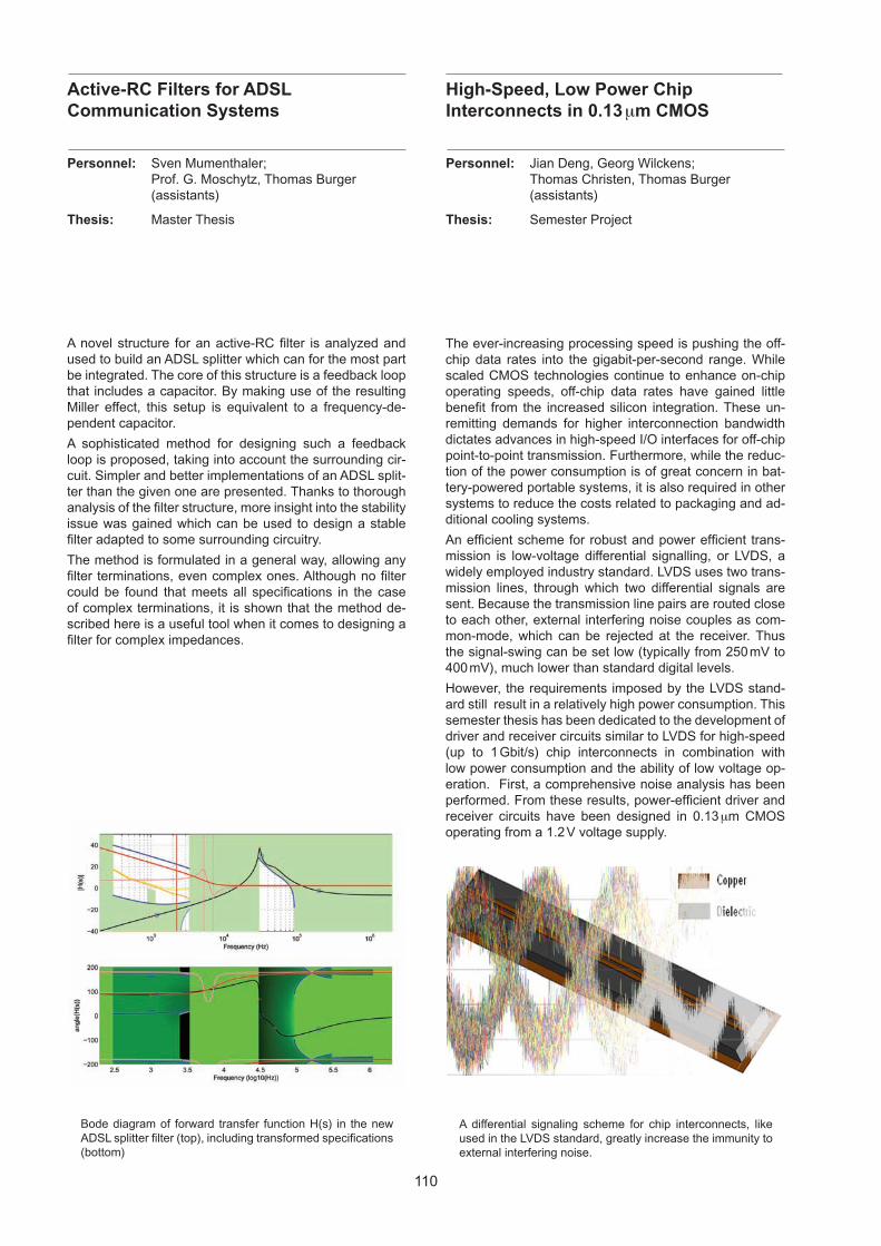
110
Personnel: Jian Deng, Georg Wilckens; Thomas Christen, Thomas Burger (assistants)
Thesis: Semester Project
High-Speed, Low Power ChipInterconnects in 0.13 mm CMOS
The ever-increasing processing speed is pushing the off-chip data rates into the gigabit-per-second range. While scaled CMOS technologies continue to enhance on-chip operating speeds, off-chip data rates have gained little benefit from the increased silicon integration. These un-remitting demands for higher interconnection bandwidth dictates advances in high-speed I/O interfaces for off-chip point-to-point transmission. Furthermore, while the reduc-tion of the power consumption is of great concern in bat-tery-powered portable systems, it is also required in other systems to reduce the costs related to packaging and ad-ditional cooling systems.
An efficient scheme for robust and power efficient trans-mission is low-voltage differential signalling, or LVDS, a widely employed industry standard. LVDS uses two trans-mission lines, through which two differential signals are sent. Because the transmission line pairs are routed close to each other, external interfering noise couples as com-mon-mode, which can be rejected at the receiver. Thus the signal-swing can be set low (typically from 250 mV to 400 mV), much lower than standard digital levels.
However, the requirements imposed by the LVDS stand-ard still result in a relatively high power consumption. This semester thesis has been dedicated to the development of driver and receiver circuits similar to LVDS for high-speed (up to 1 Gbit/s) chip interconnects in combination with low power consumption and the ability of low voltage op-eration. First, a comprehensive noise analysis has been performed. From these results, power-efficient driver and receiver circuits have been designed in 0.13 mm CMOS operating from a 1.2 V voltage supply.
A differential signaling scheme for chip interconnects, like used in the LVDS standard, greatly increase the immunity to external interfering noise.
Personnel: Sven Mumenthaler; Prof. G. Moschytz, Thomas Burger (assistants)
Thesis: Master Thesis
Active-RC Filters for ADSLCommunication Systems
A novel structure for an active-RC filter is analyzed and used to build an ADSL splitter which can for the most part be integrated. The core of this structure is a feedback loop that includes a capacitor. By making use of the resulting Miller effect, this setup is equivalent to a frequency-de-pendent capacitor.
A sophisticated method for designing such a feedback loop is proposed, taking into account the surrounding cir-cuit. Simpler and better implementations of an ADSL split-ter than the given one are presented. Thanks to thorough analysis of the filter structure, more insight into the stability issue was gained which can be used to design a stable filter adapted to some surrounding circuitry.
The method is formulated in a general way, allowing any filter terminations, even complex ones. Although no filter could be found that meets all specifications in the case of complex terminations, it is shown that the method de-scribed here is a useful tool when it comes to designing a filter for complex impedances.
Bode diagram of forward transfer function H(s) in the new ADSL splitter filter (top), including transformed specifications (bottom)
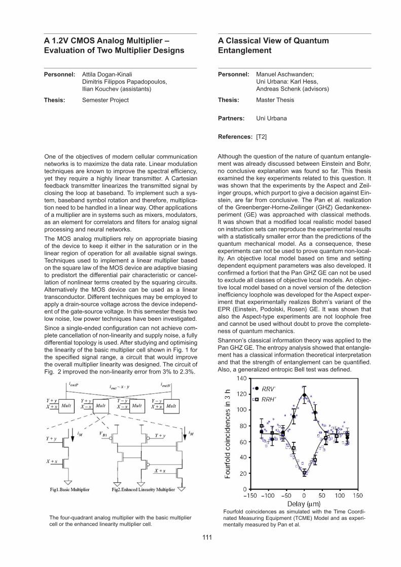
111
Personnel: Manuel Aschwanden; Uni Urbana: Karl Hess, Andreas Schenk (advisors)
Thesis: Master Thesis
Partners: Uni Urbana
References: [T2]
A Classical View of QuantumEntanglement
A 1.2V CMOS Analog Multiplier –Evaluation of Two Multiplier Designs
One of the objectives of modern cellular communication networks is to maximize the data rate. Linear modulation techniques are known to improve the spectral efficiency, yet they require a highly linear transmitter. A Cartesian feedback transmitter linearizes the transmitted signal by closing the loop at baseband. To implement such a sys-tem, baseband symbol rotation and therefore, multiplica-tion need to be handled in a linear way. Other applications of a multiplier are in systems such as mixers, modulators, as an element for correlators and filters for analog signal processing and neural networks.
The MOS analog multipliers rely on appropriate biasing of the device to keep it either in the saturation or in the linear region of operation for all available signal swings. Techniques used to implement a linear multiplier based on the square law of the MOS device are adaptive biasing to predistort the differential pair characteristic or cancel-lation of nonlinear terms created by the squaring circuits. Alternatively the MOS device can be used as a linear transconductor. Different techniques may be employed to apply a drain-source voltage across the device independ-ent of the gate-source voltage. In this semester thesis two low noise, low power techniques have been investigated.
Since a single-ended configuration can not achieve com-plete cancellation of non-linearity and supply noise, a fully differential topology is used. After studying and optimising the linearity of the basic multiplier cell shown in Fig. 1 for the specified signal range, a circuit that would improve the overall multiplier linearity was designed. The circuit of Fig. 2 improved the non-linearity error from 3% to 2.3%.
The four-quadrant analog multiplier with the basic multiplier cell or the enhanced linearity multiplier cell.
Personnel: Attila Dogan-Kinali Dimitris Filippos Papadopoulos, Ilian Kouchev (assistants)
Thesis: Semester Project
Although the question of the nature of quantum entangle-ment was already discussed between Einstein and Bohr, no conclusive explanation was found so far. This thesis examined the key experiments related to this question. It was shown that the experiments by the Aspect and Zeil-inger groups, which purport to give a decision against Ein-stein, are far from conclusive. The Pan et al. realization of the Greenberger-Horne-Zeilinger (GHZ) Gedankenex-periment (GE) was approached with classical methods. It was shown that a modified local realistic model based on instruction sets can reproduce the experimental results with a statistically smaller error than the predictions of the quantum mechanical model. As a consequence, these experiments can not be used to prove quantum non-local-ity. An objective local model based on time and setting dependent equipment parameters was also developed. It confirmed a fortiori that the Pan GHZ GE can not be used to exclude all classes of objective local models. An objec-tive local model based on a novel version of the detection inefficiency loophole was developed for the Aspect exper-iment that experimentally realizes Bohm’s variant of the EPR (Einstein, Podolski, Rosen) GE. It was shown that also the Aspect-type experiments are not loophole free and cannot be used without doubt to prove the complete-ness of quantum mechanics.
Shannon’s classical information theory was applied to the Pan GHZ GE. The entropy analysis showed that entangle-ment has a classical information theoretical interpretation and that the strength of entanglement can be quantified. Also, a generalized entropic Bell test was defined.
Fourfold coincidences as simulated with the Time Coordi-nated Measuring Equipment (TCME) Model and as experi-mentally measured by Pan et al.
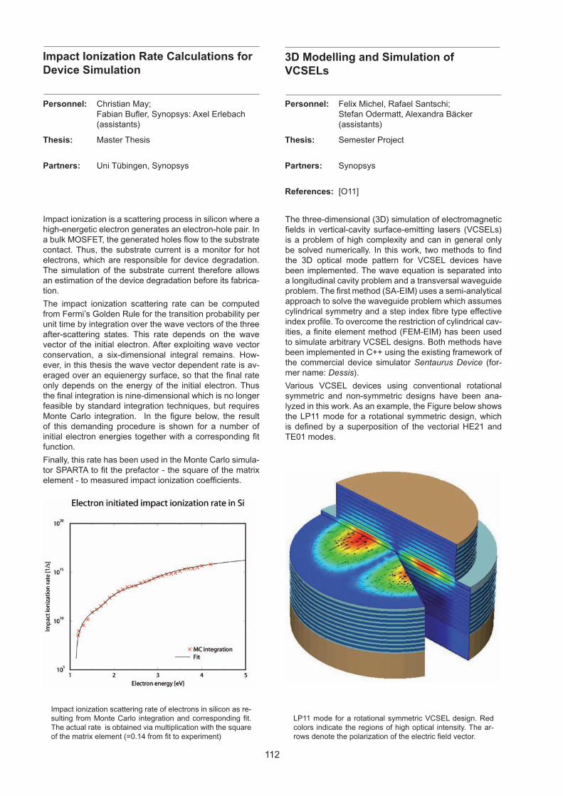
112
Personnel: Felix Michel, Rafael Santschi; Stefan Odermatt, Alexandra Bäcker (assistants)
Thesis: Semester Project
Partners: Synopsys
References: [O11]
3D Modelling and Simulation ofVCSELs
The three-dimensional (3D) simulation of electromagnetic fields in vertical-cavity surface-emitting lasers (VCSELs) is a problem of high complexity and can in general only be solved numerically. In this work, two methods to find the 3D optical mode pattern for VCSEL devices have been implemented. The wave equation is separated into a longitudinal cavity problem and a transversal waveguide problem. The first method (SA-EIM) uses a semi-analytical approach to solve the waveguide problem which assumes cylindrical symmetry and a step index fibre type effective index profile. To overcome the restriction of cylindrical cav-ities, a finite element method (FEM-EIM) has been used to simulate arbitrary VCSEL designs. Both methods have been implemented in C++ using the existing framework of the commercial device simulator Sentaurus Device (for-mer name: Dessis).
Various VCSEL devices using conventional rotational symmetric and non-symmetric designs have been ana-lyzed in this work. As an example, the Figure below shows the LP11 mode for a rotational symmetric design, which is defined by a superposition of the vectorial HE21 and TE01 modes.
LP11 mode for a rotational symmetric VCSEL design. Red colors indicate the regions of high optical intensity. The ar-rows denote the polarization of the electric field vector.
Personnel: Christian May; Fabian Bufler, Synopsys: Axel Erlebach (assistants)
Thesis: Master Thesis
Partners: Uni Tübingen, Synopsys
Impact Ionization Rate Calculations for Device Simulation
Impact ionization is a scattering process in silicon where a high-energetic electron generates an electron-hole pair. In a bulk MOSFET, the generated holes flow to the substrate contact. Thus, the substrate current is a monitor for hot electrons, which are responsible for device degradation. The simulation of the substrate current therefore allows an estimation of the device degradation before its fabrica-tion.
The impact ionization scattering rate can be computed from Fermi’s Golden Rule for the transition probability per unit time by integration over the wave vectors of the three after-scattering states. This rate depends on the wave vector of the initial electron. After exploiting wave vector conservation, a six-dimensional integral remains. How-ever, in this thesis the wave vector dependent rate is av-eraged over an equienergy surface, so that the final rate only depends on the energy of the initial electron. Thus the final integration is nine-dimensional which is no longer feasible by standard integration techniques, but requires Monte Carlo integration. In the figure below, the result of this demanding procedure is shown for a number of initial electron energies together with a corresponding fit function.
Finally, this rate has been used in the Monte Carlo simula-tor SPARTA to fit the prefactor - the square of the matrix element - to measured impact ionization coefficients.
Impact ionization scattering rate of electrons in silicon as re-sulting from Monte Carlo integration and corresponding fit. The actual rate is obtained via multiplication with the square of the matrix element (=0.14 from fit to experiment)
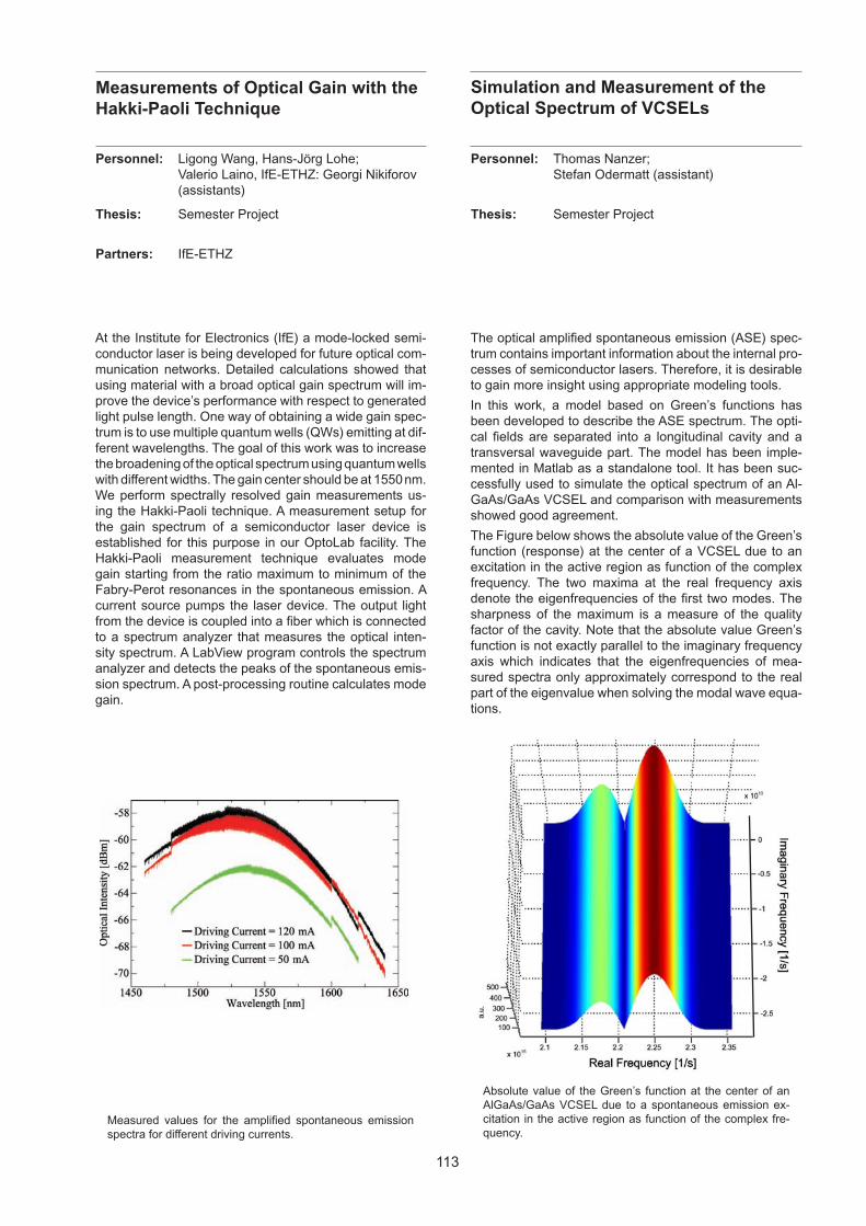
113
Personnel: Thomas Nanzer; Stefan Odermatt (assistant)
Thesis: Semester Project
Simulation and Measurement of the Optical Spectrum of VCSELs
The optical amplified spontaneous emission (ASE) spec-trum contains important information about the internal pro-cesses of semiconductor lasers. Therefore, it is desirable to gain more insight using appropriate modeling tools.
In this work, a model based on Green’s functions has been developed to describe the ASE spectrum. The opti-cal fields are separated into a longitudinal cavity and a transversal waveguide part. The model has been imple-mented in Matlab as a standalone tool. It has been suc-cessfully used to simulate the optical spectrum of an Al-GaAs/GaAs VCSEL and comparison with measurements showed good agreement.
The Figure below shows the absolute value of the Green’s function (response) at the center of a VCSEL due to an excitation in the active region as function of the complex frequency. The two maxima at the real frequency axis denote the eigenfrequencies of the first two modes. The sharpness of the maximum is a measure of the quality factor of the cavity. Note that the absolute value Green’s function is not exactly parallel to the imaginary frequency axis which indicates that the eigenfrequencies of mea-sured spectra only approximately correspond to the real part of the eigenvalue when solving the modal wave equa-tions.
Absolute value of the Green’s function at the center of an AlGaAs/GaAs VCSEL due to a spontaneous emission ex-citation in the active region as function of the complex fre-quency.
Personnel: Ligong Wang, Hans-Jörg Lohe; Valerio Laino, IfE-ETHZ: Georgi Nikiforov (assistants)
Thesis: Semester Project
Partners: IfE-ETHZ
Measurements of Optical Gain with the Hakki-Paoli Technique
At the Institute for Electronics (IfE) a mode-locked semi-conductor laser is being developed for future optical com-munication networks. Detailed calculations showed that using material with a broad optical gain spectrum will im-prove the device’s performance with respect to generated light pulse length. One way of obtaining a wide gain spec-trum is to use multiple quantum wells (QWs) emitting at dif-ferent wavelengths. The goal of this work was to increase the broadening of the optical spectrum using quantum wells with different widths. The gain center should be at 1550 nm. We perform spectrally resolved gain measurements us-ing the Hakki-Paoli technique. A measurement setup for the gain spectrum of a semiconductor laser device is established for this purpose in our OptoLab facility. The Hakki-Paoli measurement technique evaluates mode gain starting from the ratio maximum to minimum of the Fabry-Perot resonances in the spontaneous emission. A current source pumps the laser device. The output light from the device is coupled into a fiber which is connected to a spectrum analyzer that measures the optical inten-sity spectrum. A LabView program controls the spectrum analyzer and detects the peaks of the spontaneous emis-sion spectrum. A post-processing routine calculates mode gain.
Measured values for the amplified spontaneous emission spectra for different driving currents.
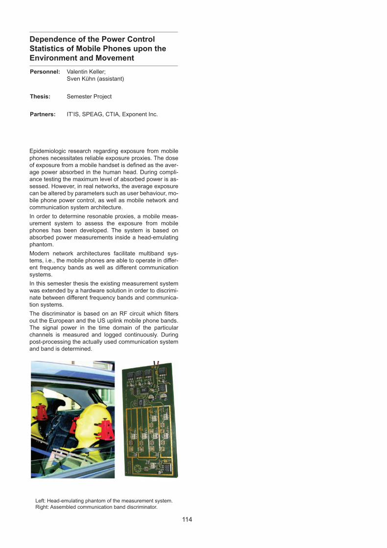
114
Dependence of the Power ControlStatistics of Mobile Phones upon theEnvironment and Movement
Epidemiologic research regarding exposure from mobile phones necessitates reliable exposure proxies. The dose of exposure from a mobile handset is defined as the aver-age power absorbed in the human head. During compli-ance testing the maximum level of absorbed power is as-sessed. However, in real networks, the average exposure can be altered by parameters such as user behaviour, mo-bile phone power control, as well as mobile network and communication system architecture.
In order to determine resonable proxies, a mobile meas-urement system to assess the exposure from mobile phones has been developed. The system is based on absorbed power measurements inside a head-emulating phantom.
Modern network architectures facilitate multiband sys-tems, i.e., the mobile phones are able to operate in differ-ent frequency bands as well as different communication systems.
In this semester thesis the existing measurement system was extended by a hardware solution in order to discrimi-nate between different frequency bands and communica-tion systems.
The discriminator is based on an RF circuit which filters out the European and the US uplink mobile phone bands. The signal power in the time domain of the particular channels is measured and logged continuously. During post-processing the actually used communication system and band is determined.
Left: Head-emulating phantom of the measurement system. Right: Assembled communication band discriminator.
Personnel: Valentin Keller; Sven Kühn (assistant)
Thesis: Semester Project
Partners: IT’IS, SPEAG, CTIA, Exponent Inc.
115
PhD Theses – Abstracts
This thesis presents specific studies on the design of D/A converters finalized towards the implementation of two dif-ferent design examples in 0.18 mm CMOS technology.
The initial study addresses the problem of determining which is the requirement for the matching accuracy of the unit currents of a generic current-steering converter so that either a specified integral or differential non-linearity, or a specified effective number of bits, can be ensured with a minimum yield. The investigation then proceeds with the analysis of the principal distortion mechanisms for the same type of converter and concludes with a compre-hensive analysis of the effects of the jitter on the signal re-produced by a D/A converter with different pulse formats. In particular the case of oversampled noise shaping D/A converters is treated.
In the first design example, calibration is used truly in back-ground to overcome the limited matching accuracy of the current sources of the upper segment of a current-steer-ing D/A converter. The calibrated cells are implemented as floating current sources. With such a scheme the current is available at both ends of the source so that, while at one end the current is always steered to the output nodes, at the other end the same current is compared against a reference and trimmed to the correct value. The calibra-tion is stored in a capacitor connected to a gate of a MOS transistor acting as a trimming current source and is pe-
riodically refreshed. The converter achieves an outstand-ing static linearity of 14-bits and thanks to a return-to-zero pulse format is also capable of delivering spectrally pure signals at high frequency. With 200 MHz clock frequency and the return-to-zero scheme enabled, a SFDR better than 60 dBc is maintained up to 90 MHz signal frequency.
In the second design example, an architecture that does not rely on stringent component matching to reconstruct linearly an oversampled signal from a sigma-delta modu-lator is presented. A 16 times oversampled signal from a 4th-order multi-bit cascaded sigma-delta digital modulator is reconstructed with a filter composed by a semidigital/digital transversal filter and a recursive filter in switched-capacitor (SC) technique. A linear D/A conversion is achieved by preceding the critical reconstruction phase in the recursive SC filter with a coarse signal reconstruc-tion by means of the semidigital/digital FIR filtering. The complete signal reconstruction performed in the analog discrete domain ensures also robustness against jitter. With a SNR of 78 dB and a SFDR ranging from 73 dB to 80 dB within a 1.104 MHz signal band, the proposed system is suitable for broadband applications. A MTPR > 70 dB measured with 15 dB PAR and the out-of-band spurious emission levels below the ADSL-CO mask prove the feasibility.
Prof. Dr. Q. Huang, ETH Zürich, examinerProf. Dr. H.-A. Löliger, ISI-ETHZ, co-examiner
Diss. ETH-Nr. 16294ISBN 3-89191-055-6
This thesis is a contribution to the development of a high-performance CMOS transmitter for mobile UMTS hand-sets. In this context, high-performance stands for the abil-ity to fulfill all UMTS specifications at the lowest possible power consumption.
The architecture of choice is direct up-conversion be-cause it requires the least number of external filters. This maximizes the integration level. A limiting factor is the car-rier leakage that is a direct consequence of the selected direct up-conversion architecture. The carrier leakage has a detrimental effect on the signal quality and may severely restrict the gain control range. Several techniques are shown that can be used to keep the carrier leakage low. Calibration methods can bring the carrier leakage to very low levels. Unfortunately, they are not very robust and re-calibrations need to be done every now and then. The final
solution simply attributes most of the gain control range to the RF stages. Thus, the carrier and the wanted signal are treated in the same manner and the quality of the signal is maintained even at very low gain settings. The enabler of this solution is a 2 GHz pre-amplifier that can sustain the required gain step accuracy over the full gain control range. Additionally, a pre-amplifier design in 90 nm CMOS is presented that performs an on-chip differential to single-ended conversion and provides a 50 Ohm match.
The built CMOS transmitter delivers a WCDMA output power of 2 dBm at a power consumption of 82 mW. The carrier leakage-free gain control range is a remarkable 77 dB in 1 dB steps. The gain step accuracy is better than 0.5 dB. Together with an external power amplifier and du-plex filter the overall transmitter qualifies for UMTS power class 3 classification with an output power of 24 dBm.
WCDMA Transmitter Design in Deep-Submicron Technology
David Tschopp
Prof. Dr. Q. Huang, ETH Zürich, examinerProf. Dr. H. Jäckel, ETH Zürich, co-examiner
Diss. ETH-Nr. 15945ISBN not yet available
D/A Converters on CMOS Technology
Pier-Andrea Francese
116
The integrated circuit manufacturing technology improves almost daily, and enables designers to construct circuits that are both smaller and are able to work faster. While this increases the performance and allows more functions to be integrated on to micro-chips, it also poses significant challenges to designers.
Conventional digital circuits rely on a global clock signal to function. These circuits are called synchronous, as the timing of all operations of the circuit are derived from the global clock signal. As a result of the technological im-provements with each new generation of integrated cir-cuits, both the clock rate, and the number of clock connec-tions within the micro-chip continue to increase. Reliably distributing the clock signal over the micro-chip has be-come one of the leading challenges of modern digital sys-tem design.
The Globally-Asynchronous Locally-Synchronous (GALS) system design has been developed to address this prob-lem. A GALS system consists of several sub-designs, called GALS modules, that have their own local clock gen-erators. Each module by itself is synchronous and can be
designed using a conventional design methodology. What is required is a reliable method to exchange data between these independent GALS modules. Instead of a global clock signal, GALS systems use an asynchronous hand-shaking protocol between GALS modules. Each GALS module contains additional control circuitry that briefly pauses the local clock to ensure data integrity during these transfers.
The feasibility of the GALS design methodology, and an extension of the methodology to support multi-point con-nections between GALS modules has been investigated in two previous Ph. D. theses by J. Muttersbach and T. Villiger. In this thesis, the GALS methodology has been
applied to improve the security of cryptographic systems.
Cryptographic systems are an integral part of modern digital society providing solutions to secure information from unauthorized access. In its most basic form, a cryp-tographic algorithm uses a secret key (a series of 0’s and 1’s) to transform information so that it can only be deci-phered by others who have the same secret key.
There are several well established algorithms, like the Ad-vanced Encryption Standard (AES), that provide a very high level of security. However, once this algorithm is implemented, in either hardware or software, it acquires several physical properties (heat, power consumption etc) that can be monitored during operation. Starting in 1999, it was shown that it is possible to extract the secret key of a cryptographic system by only monitoring the power con-sumption. This is a very serious problem, and immediately a number of countermeasures were developed against these so called side channel attacks.
In this thesis, the design of a GALS based AES implemen-tation is presented. The design consists of three independ-ent GALS modules which have a local clock generator that is able to change its period randomly. By combining this architecture with several well-known countermeas-ures against side channel attacks, the security of the AES implementation has been improved considerably.
This work represents the first application of GALS to im-prove the side-channel security of a cryptographic system. A mature GALS design flow, which is mainly based on in-dustry standard electronic design automation tools, has been used to fabricate the circuit. Measurement results showed that the performance metrics (throughput, area, power consumption) of the GALS integration are compa-rable to circuits that were designed using conventional synchronous methods.
GALS System Design: Side Channel Attack Secure Cryptographic Accelerators
Frank K. Gürkaynak
Prof. Dr. W. Fichtner, ETH Zürich, examinerProf. Dr. Yusuf Leblebici, LSM-EPFL, co-examiner
Diss. ETH-Nr. 16351ISBN 3-86628-065-3
Multiple-input multiple-output (MIMO) systems are widely recognized as the enabling technology for future wireless communication systems. In particular the use of spatial multiplexing allows to achieve a linear increase in capacity with the minimum of the number of antennas employed at the transmitter and at the receiver. Unfortunately, these capacity gains are bought dearly at the expense of higher silicon complexity at the receiver. In particular, the separa-tion of the spatially multiplexed streams poses a consider-able research challenge.
So far, most publications in this field have focused on complexity reduction of algorithms with software program-mable architectures in mind. However, such implementa-tions can not meet the requirements of wideband MIMO systems and the corresponding optimizations are often not immediately applicable or are not even advantageous for dedicated VLSI circuits. Unfortunately, even the very
few reported VLSI implementations of MIMO detection are not able to meet the requirements (in terms of through-put or latency) of envisioned future MIMO communication systems.
Hence, in this thesis we focus on the VLSI implementation of MIMO detection algorithms for spatial multiplexing. In particular, linear and successive interference cancellation, exhaustive search maximum likelihood, and sphere and K-best decoding are considered. To this end, correspond-ing optimized algorithms and techniques for complexity reduction are developed which are specifically tailored to the requirements of VLSI circuits. Based on these consid-erations, novel low-complexity VLSI architectures are pro-posed. Finally, our implementations (which are currently the fastest reported implementations of MIMO detection) provide reference for the true silicon complexity of this kind of algorithms.
Prof. Dr. W. Fichtner, ETH Zürich, examinerProf. Dr. M. Rupp, TU Vienna, co-examiner
Diss. ETH-Nr. 16427ISBN 3-86628-066-1
VLSI Circuits for MIMO Communication Systems
Andreas Burg
117
Physical objects called moments of the inverse scatter-ing operator (MISO) of the Boltzmann equation (BE) allow to compute all quantities which appear in semiconductor transport theory (e.g. mobilities, Hall factors, Langevin noise sources, ...) in an exact way, i.e. without using the well-known relaxation time approximation.
In the first part, the existence and uniqueness of the MISOs are proven, and a numerical algorithm is given to actually compute all of them. Some of the most important applica-tions of the MISOs include amongst others the computa-tion of Hall factors, and the computation of exact Langevin noise sources. They are further developed to compute the solution to the space-homogeneous Boltzmann equation for small field intensities to any order in the electric and magnetic field. Another application is the derivation of a new iterative scheme for the one-particle Monte Carlo (MC) method, which allows to take into account genera-tion recombination processes, which is not possible with the classical method. The last application presented is the determination of the transition from the low- to the high-field regime.
The second part deals with fluctuation theory: Using the concept of MISO, exact formal expressions are derived for the impedance field method (IFM) as well as for the acceleration fluctuation scheme. This allows to compare both methods on the same basis and, therefore, to better understand their meanings, implications, analogies and differences.
It may be concluded that the IFM contains a formal flaw that seems not to affect the present applicability of the
method, but should be considered during the develop-ment of future applications.
The third part introduces the numerical methods and physical models underlying the calculation of a series of physical properties of silicon and silicon devices further illustrated in part four. The finite element method was cho-sen to compute the solutions to the transport model (TM) equations. Using the electric potential and quasi-Fermi potentials as variables and avoiding Bernoulli polyno-mials, leads to a suitable formulation for solving the TM equations. In contrast to what has been claimed in the literature, the presented method is appropriate to readily solve such TM equations.
In order to use the MISOs in the far-from-equilibrium re-gime, a MC method has been used to solve the BE. Cou-pling of a MC method with the MISO allows not only to compute stationary states, but may even give access to Y-parameters and noise.
The last part deals with the application of the developed theory to bulk silicon and silicon devices. First, MISOs of interest are computed for the physical models contained in our in-house TM and MC simulator, SimnIC, for fre-quency dependent and independent scattering operators. Then, the MISOs are used to extract transport coefficients and noise sources in bulk silicon for low- and high-electric fields. Simulations of a simple N+NN+ structure previous-ly studied in the literature underlines the applicability of MISOs for semiconductor small-signal analysis and noise modelling.
Prof. Dr. W. Fichtner, ETH Zürich, examinerProf. Dr. M. Macucci, Uni Pisa, co-examiner
Diss. ETH-Nr. 16376ISBN 3-86628-062-9
Prof. Dr. W. Fichtner, ETH Zürich, examinerProf. Dr. G. Baccarani, Uni Bologna, co-examiner
Diss. ETH-Nr. 16228ISBN not yet available
Quantum-Mechanical Modeling of Transport Parameters for MOS Devices
Timm HöhrThe ongoing evolution of integrated circuits is based on the miniaturization of the individual devices. The feature sizes that are routinely implemented by today’s manufac-turing technology already belong to the domain of quan-tum effects. On one hand this poses additional problems for traditional device concepts but on the other hand it paves the road towards new functional principles. For as-sessing either aspects, models are needed for simulators which have become an important tool in both device and process engineering.
Topic of this thesis are the implications of quantization on transport parameters in drift-diffusion-based numerical descriptions of semiconductor devices. To this end, the device simulator DESSIS is used, especially its enhance-ments to model quantum effects which comprise a self-consistent Schrödinger-Poisson solver for one-dimen-sional quantization effects and the quantum drift-diffusion (QDD) model.
In the first part of this work, the QDD model is applied to tunneling through MOS gate oxides and double bar-rier devices. For both structures the “tunneling” charac-teristics exhibit regions of negative differential resistance which was identified as a modeling artifact. These results
indicate that the QDD-description of tunneling is of only very limited use.
The second part deals with modeling of Shockley-Read-Hall (SRH) recombination, which is enabled by multipho-non processes between bands and deep trap levels in the gap of the semiconductor, in the presence of quantization. The corresponding density of states which is used in the description of the carrier densities must also be applied to the SRH-lifetimes, i.e. they have to account for an ad-ditional energetic separation from the trap levels. This in turn causes a corresponding change in the SRH rate with respect to the usual description.
The third part is devoted to modeling of the drift mobility in MOS channels. The main focus is put onto Coulomb scattering at ionized impurities located in the substrate as well as in the polysilicon gate. The influence from the lat-ter is commonly named “remote charge scattering” (RCS) and suspected of contributing to the mobility degradation observed in thin-oxide devices. However, in the treat-ment presented here, which includes screening by mobile charge in the gate, RCS was found not to have a great impact.
Computation of Semiconductor Properties Using Moments of the Inverse Scattering Operator of the Boltzmann Equation
Simon Brugger
118
As a result of technology scaling and the broadening of automated handling in production, failures in ICs caused by Charged Device Model (CDM) Electrostatic Discharge (ESD) are an increasingly important reliability issue. To-day, a significant portion of ESD field returns are due to damages originating from CDM stress. To be competitive in the fast moving semiconductor industry, companies have to design ICs which meet state-of-the-art require-ments for CDM robustness on the one hand and ensure first silicon success on the other. Computer aided design (CAD) models and tools support in fulfilling these require-ments. The goal of this thesis is to provide comprehen-sive information for coping with the challenges of accurate CDM circuit simulation.
In case of a CDM event, the charge carriers which are dispersed over the complete IC and package discharge through the path with the lowest impedance. Apart from power bus and protection devices, this path can lead through substrate and other parasitic physical layers. The relevance of these parasitic elements for CDM circuit sim-ulation is demonstrated in this thesis. Also, the behavior of ICs during CDM discharges is strongly affected by the package. This is primarily attributable to the package ca-pacitances which form the main charge source for a CDM event. Due to the high frequencies associated with such events, the discharge behavior is also influenced by the inductive, capacitive and resistive parasitics of package and CDM measuring equipment. The high electric fields between the CDM tester pin and the IC pin can result in a discharge arc which reduces the rise time and the amplitude of the discharge current. This work introduces approaches for modeling all these elements and demon-strates that accounting for them in the simulation setup is essential for achieving correct simulation results.
When pn junctions are biased with fast transient cur-rent signals, a voltage overshoot can occur across these devices. In forward bias, this effect is known as forward recovery effect. The impact of this effect on the CDM behavior of devices is investigated with measurements and device simulation. Compact models that reflect this transient turn-on behavior effectively are presented. In reverse bias, an increase of the breakdown voltage of re-versed biased pn junctions can be observed for trigger
pulses with voltage slopes in the CDM time domain. The physical mechanism causing the delayed breakdown is investigated. The relevance of this effect for the behavior of ICs during CDM discharges is discussed.
A newly developed automated method for extracting tran-sient, high-current model parameters for circuit simulation of CDM ESD events is presented. The procedure is per-formed with transient signals obtained from very-fast TLP (Transmission Line Pulse) measurements. This method utilizes the maximum achievable accuracy of the currently available characterization methods, which reach their lim-its in the CDM time and current domain. Hence, the pro-posed method is suitable for determining parameters of compact models that include CDM specific device physi-cal effects.
The applicability of the proposed CDM simulation method for predicting the CDM behavior of ICs correctly is evaluat-ed with two case studies in different smart power process generations. Firstly, a CDM specific failure mechanism was investigated for an input protection structure in a 0.8 µm technology. CDM tests revealed unexpected depen-dency of the CDM robustness on design variations. This work demonstrates that the complex, CDM specific failure mechanism can be reproduced accurately with circuit sim-ulation. Comparison with device simulation and measure-ment results showed that even the failure levels can be determined correctly with circuit simulation. Secondly, the capability of proposed simulation method to predict the CDM robustness of integrated circuits is verified for varia-tions of an ESD evaluation circuit in a 0.35 µm technol-ogy. These circuits were designed to enable the analysis and optimization of ESD protection strategies in an early design phase during the introduction of a new technol-ogy. Detailed cross-checks are performed between CDM tests of different design variations and the corresponding results derived from circuit simulation. Failure modes and locations which were determined using results from func-tional measurements are confirmed with failure analysis. From these results, the conclusion can be drawn that by employing the proposed CDM simulation method, weak circuit elements can be discovered and corrected before silicon is available.
Charged Device Model (CDM) ESD in ICs: Physics, Modeling, and Circuit Simulation
Melanie Etherton
Prof. Dr. W. Fichtner, ETH Zürich, examinerDr. W. Stadler, Infineon, co-examiner
Diss. ETH-Nr. 16354ISBN 3-86628-067-X
In the present work, the imaging and the quantitative doping profiling capabilities of Scanning Capacitance Mi-croscopy (SCM) and Scanning Spreading Resistance Mi-croscopy (SSRM) for nanometer scale devices are investi-gated. Special attention has been paid to the development and the optimization of dedicated processes for the prep-aration of suitable cross-sectioned samples. In fact, the control of surface characteristics such as roughness, state density, and fixed charges has been demonstrated to be a crucial factor for reproducible and quantitative results. The exploration of the physical limits of the SCM tech-nique has been assisted by two- and three-dimensional simulations of the measurement process. In particular, de-vice simulation has been applied to quantify the maximum
achievable accuracy in the determination of doping pro-files and in the delineation of the electrical junction. In this respect, a novel technique is proposed, which represents an efficient alternative to the capacitance spectroscopy for the quantitative localization of the electrical junction in bipolar samples. The capabilities of SCM have been assessed with own measurements and with experimental data from a round robin experiment, which has involved several European laboratories. SSRM measurements have been carried out on the same samples character-ized by SCM and the peculiarities of both techniques are discussed. In particular, this work points out the impact of the different parasitic components that contribute to the formation of the SSRM signal, leading to the observed de-
Scanning Probe Techniques for Dopant Profile Characterization
Maria Stangoni
119
PhD theses can be ordered from:
Hartung-Gorre Publisher Phone: +49 7533 97227Säntisblick 26 Fax: +49 7533 97228D-78465 Konstanz E-mail: [email protected] Web: http://www.Hartung-Gorre.de
Numerous experiments addressing the possible nega-tive health effects of EMF have been conducted in recent years. Various research groups have performed animal, cell and human studies with different scientific approach-es. Several experiments have turned out to be of limited value due to severe shortcomings in the exposure setup. A major point of criticism is the lack of mature controlling software of most setups, having some important draw-backs.
The first part of this PhD thesis describes the basic re-quirements of modern exposure systems (in vitro, in vivo and human). Analyzing these requirements reveals the importance of well-adapted controlling software. Only systems with sophisticated controlling software can meet all requirements. Up to the present, no exposure system with software tightly controlling the experiments has been developed nor described in the literature. The purpose of this topic is to close this gap and to provide designers of exposure setups with basic guidelines for the creation of controlling software.
The realized controlling software was applied in more than 20 different worldwide laboratory studies for cells, animals and humans. The controlling software enabled to perform animal studies under NTP-like (National Toxicology Pro-gram) GLP (Good Laboratory Practice) conditions. The derived mathematical GSM signal model and the imple-mentation of this model became standard in BIOEM (bio-electromagnetic) research. This signal model represents the first exposure scenario that applies temporal changes of different modulation schemes as occurring in an ac-tual phone conversation. This signal contains a cocktail of low-frequency modulation components. Studies in the past neglected the influence of these low-frequency com-ponents.
Based on the experience gained during the implementa-tion of several large-scale software projects as presented in the first part of this thesis, the importance of the ap-plication of suitable software engineering methodologies became clear and is analyzed in the second part.
Today software engineering includes two sets of funda-mentally different methodologies: heavyweight method-ologies and agile methodologies. Heavyweight method-ologies follow the traditional way of constructing software. The core of heavyweight methodologies constitutes the separation of design and implementation activities. Agile methodologies on the other hand focus on incremental software development, close cooperation with the cus-tomer, simple solutions and fast reaction time to changing conditions. The second part of this thesis describes the specific heavyweight and agile methodologies based on the methodologies’ most important features. Similarities and varieties are identified and discussed. The descrip-tion of the methodologies serves as the basis for the sub-sequent evaluation of the presented software engineering methodologies for practical use.
The evaluation has shown that no methodology is inher-ently suitable for all situations and for all organizations. Each methodology has its strengths and weaknesses. However, their strengths are present in different situa-tions. Agile methodologies seem to be particularly suitable in situations where the requirements are likely to change in the future, whereas heavyweight methodologies deploy their full potential if future requirements (performance, exception handling, functionality) are known and can be specified in detail.
Prof. Dr. W. Fichtner, ETH Zürich, examinerProf. Dr. N. Kuster, IT’IS/ETH Zürich and Dr. Michael Burkhardt, Sunrise Zürich, co-examiners
Diss. ETH-Nr. 16346ISBN not yet available
Prof. Dr. W. Fichtner, ETH Zürich, examinerDr. V. Ranieri, IMM Catania,co-examiner
Diss. ETH-Nr. 16024ISBN 3-89649-991-2
viation of the measured characteristics from the curves predicted by the spreading theory. It is also shown that for this reason the quantitative doping profiling by SSRM requires an accurate case-by-case calibration. The SSRM measurement process has been simulated in two and in three dimensions both to quantify the weight of the para-sitic series resistances and to ascertain the intrinsic limits of the technique in the delineation of the electrical junction in bipolar samples. These simulations demonstrate that due to the strong modification of the local carrier density through the injecting tip, SSRM cannot reach the same junction delineation capabilities as for SCM. Progress has
also been made in increasing the accuracy of the con-version of the free carrier SCM and SSRM profiles into the related doping profiles. For this purpose, a numerical solution scheme of the reverse modelling problem based on the use of Artificial Neural Networks has been devel-oped. The assessment of both techniques demonstrates that SCM and SSRM exhibit a large degree of comple-mentarity. SCM has shown to be superior to SSRM in the case of complex large bipolar structures, whereas SSRM provides the excellent lateral resolution required to image nanometer scale devices.
Controlling Software for EMF Laboratory Studies
Walter Oesch
120
Summer Semester 2005
Beat Kessler Design of a Linear Regulator for a Mobile Phone Baseband and Audio Interface
Christoph Studer Sphere Decoding with Resource Constraints
Chen Wang A Low-Power Analog-to-Digital Converter for Ultra-Wide-Band Applications
Stefan Schuler Medium-Access Control for MIMO-OFDM Testbed Christian Hitz
Vedran Galijas MIMO Channel Emulator
Markus Wenk VLSI Implementations of Reduced-Complexity Maximum-Likelihood Algorithms Martin Zellweger for MIMO Systems
Christian May Impact-Ionization Rate Calculations for Device Simulations
Roger Kaspar Design of a Lowest-Latency Multi-Channel Audio Compression/Decompression Algorithm Sandro Schifferle
Philippe Schaller Implementation Issues of Hybrid Soft-/Hardware MIMO-OFDM MAC
Thierry Gschwind FPGA Pre-Processing for Image Processing System
Winter Semester 2005/2006
Frederic Poncioni RF Frontend for MIMO Testbed Pascal Wildbolz
Mathias Meyer Modeling and Design of Network-on-Chip Allocation Policies
Stefano Cuncu Carrier Mobility in Silicon at High Temperatures
Yves Kunz A DC-DC Converter for Wireless Applications in 0.13 µm CMOS
Wolfgang Haid Algorithms for MIMO-OFDM Parameter Estimation and Tracking
Attila Dogan Design and Implementation of a Fast Programmable k-Selector
Master Theses – Overview

121
Summer Semester 2005
Fabian Brugger Differential Power Analysis Attack Accelerator Wesley Allred
Valentin Keller Dependence of the Power Control Statistics of Mobile Phones upon the Environment and Movement
David Scheiner High-Performance IP Connectivity for a MIMO Communication System
Attila Dogan Evaluation of Two Analog Multiplier Designs in 1.2 V CMOS
Bin Yan Turbo En/Decoder for UMTS
Simon Mall System Design for EWA Splat Rasterizer
Roman Stampfli Multi-Standard and Broadband CMOS LNAs for Wireless Receivers Stefan Schmid
Georg Wilckens High-Speed Low-Power Chip Interconnects in 0.13 µm CMOS Jian Deng
Felix Michel 3D Modelling and Simulation of Vertical-Cavity Surface-Emitting Lasers Rafael Santschi
Christian Zimmermann 2 x 2 MIMO Acoustic Communication system Pascal Wildbolz
Wolfgang Haid MIMO-OFDM Frequency-Offset Estimation
Winter Semester 2005/2006
Yan Wanfeng New One-Particle Monte-Carlo Method: Generation-Recombination Processes and Quantum Correction
Reto Schwarz Algorithms for Multiplier Synthesis
Guergui Nikiforov Simulation and Measurement of Quantum-Well Optical Gain
Ton Cvetic LDPC Decoder for MIMO Moritz Mattmann
Sandra Märchy Interpolation of Flow Sensor Data Tamara Ulrich
Andreas Looser Virtual Analog Synthesizer: A Digital ASIC Implementation Andreas Gysi David Christen
Bruno Spori On-Chip IP Address Lookup Christoph Rüegg
Nicolas Vollmar Digital Up/Down Conversion for 4x4 MIMO System Özge Gürsoy
René Blattmann Crypto Hardware Realizations of eSTREAM Candidates (1) Nico Bernold
Marcel Marghitola Crypto Hardware Realizations of eSTREAM Candidates (2) Vicky Gooden
Tobias Blaser Wavelet-based Compression using SPIHT Algoriithm Stephan Senn Philipp Stadelmann
Daniel Krähenbühl Low-Power Optimization for an Adaptive Directional Microphone for Hearing Aids Franz Zürcher
Student Projects – Overview

122
André Meyer Channel Estimation for MIMO-OFDM Thomas Peter
Rafael Baur Interpolation-based QR Decomposition for MIMO-OFDM Johannes Güttinger
Isak Lichtenstein Radix-2 logMAP Turbo Decoder for HSDPA Claudio Fölmli
Claudio Pagnamenta Low-Power Viterbi Decoder with Resonant Clocking Fabio Coduri Manuel Arrigo
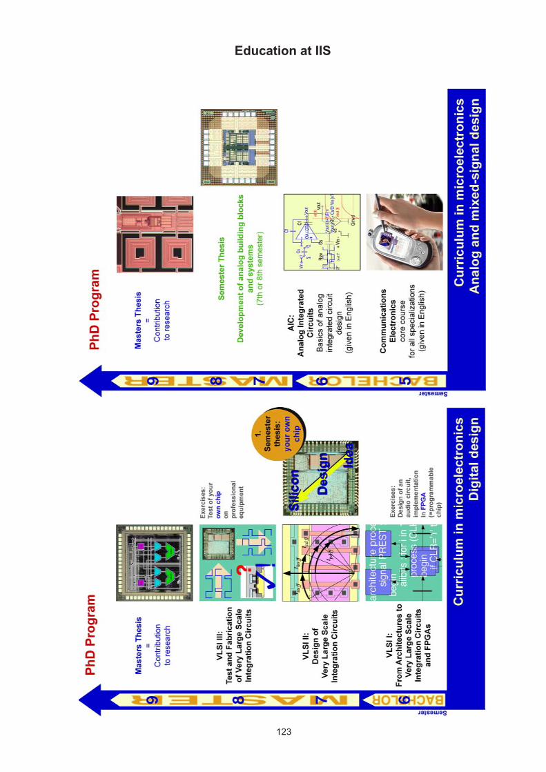
123
Education at IIS
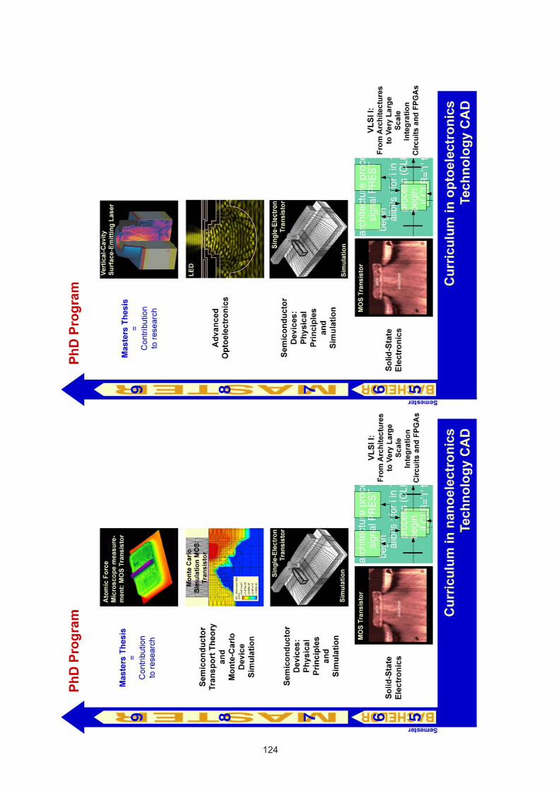
124
125
Halbleiterbauelemente 4th Sem. Semiconductor Devices EE
A. Schenk
This lecture gives an introduction to the basics of modern semiconductor devices for micro-, opto-, and power-electronics. It bases on semiconductor physics and covers band structures, band models, dispersion relations, statistics, transport equa-tions, macroscopic models, and the characteristics of silicon and other semiconductors. An overview on device families is presented.
The part on technologies covers the properties of materials, and introduces the steps of modern process technologies as well as packaging. To understand the basic principles of devices, ohmic and rectifying contacts, physical and electrical characteristics of pn junctions, and types of diodes are explained. The lecture continues with the bipolar transistor’s func-tion, working regions, characteristic diagrams, and its simulation. MOS devices are treated based on band diagrams, and the MOSFET behavior is deduced. Power devices, their working regions and static and dynamic behavior are followed by examples of optoelectronic devices as photo conductor, photodiode, LED, and fiber. Semiconductor measurement and characterization methods conclude the course.
Kommunikationselektronik 5th Sem. Communications Electronics EE
Q. Huang
This course provides basic design and circuit techniques for communications electronics. As a starting point, bipolar and MOS transistors are reviewed. The discussion of circuit design begins with basic amplifier topologies, impedance matching concepts, and a bit of two-port theory. Important non-ideal aspects such as non-linearity and noise are discussed. This sets the ground for more involved topics. Important building blocks of communications equipment, such as mixers and oscil-lators, are examined in detail. The discussions include the basic topologies, mathematical descriptions, and a thorough analysis of non-ideal behavior, from which finally guidelines for the design can be derived.
The exercises form an integral part of this course. The definitions and concepts presented in the lecture will be reinforced by small design examples, therefore providing a link between the theoretical description and real-world problems.
Solid State Electronics 5th Sem. Festkörperelektronik EE
B. Witzigmann
The lecture Solid State Electronics explains the fundamental physical effects and properties for the operation of modern semiconductor devices. The focus is put on the solid state description by means of statistics, classical, and quantum phys-ics. Device aspects play only a minor role, however, students learn the fundamentals for studying device operation in subse-quent advanced lectures. In the beginning an introduction to quantum mechanics principles is given that helps understand the basic concepts from an engineering standpoint. The goal of the lecture is to get familiarized with the unique properties of semiconductors using a microscopic view, such as crystal structure, doping, energy bands, carrier dynamics and magnetic and optical properties.
VLSI I: Von Architektur zu hochintegrierter Schaltung und FPGA 6th Sem. VLSI I: From Architectures to Very Large Scale Integration Circuits and FPGAs EE/CS/Phys/CSE
N. Felber, W. Fichtner, H. Kaeslin
As becomes clear from the subsequent list of topics, the first course in this series of three is mainly concerned with system-level issues of VLSI. Terminology, overview on design methodologies and fabrication avenues, levels of abstraction used for circuit description and simulation, VLSI design flow, dedicated VLSI architectures, how to obtain an architecture for a given processing algorithm, architectural transformations for meeting throughput, area, and power requirements. Hardware De-scription Languages (HDL) and their underlying concepts, VHDL for simulation and synthesis, the IEEE-1164 logic system, Register Transfer Level (RTL) synthesis. Timing models, Anceau diagrams, functional verification of digital circuits and sys-tems, building blocks of digital VLSI circuits, case studies of actual circuits, comparison with microprocessors and DSPs.
During the exercises students learn how to model digital ICs with VHDL. They write testbenches for simulation purposes and synthesize gate-level netlists for ASICs and FPGAs.
VLSI II: Entwurf von hochintegrierten Schaltungen 7th Sem. VLSI II: Design of Very Large Scale Integration Circuits EE/CS/Phys/CSE
N. Felber, W. Fichtner, H. Kaeslin
The second course begins with a thorough discussion of various technical aspects at the circuit and layout level. It then moves on to economic issues of VLSI. Topics include: limitations of functional design verification, techniques for improving controllability and observability, design for test, block isolation, scan-path techniques, partial scan and its caveats. Evalu-
Lectures

126
ation of various synchronous clocking disciplines, skew margins, clock distribution techniques. Asynchronous inputs, data inconsistency and metastability problems, synchronization. Cell libraries, Process-Temperature-Voltage (PTV) variations, transistor models, characteristics of CMOS inverters, complex gates. Power estimation and low-power design. Layout para-sitics, transport delay, switching currents, ground bounce, controlling noise problems, power distribution, floorplanning, chip assembly. Layout design at the mask level, symbolic layout. Timing verification, physical design verification. Cost structures of microelectronics design and fabrication, avenues to low-volume fabrication, management of VLSI projects.
Exercises are concerned with physical design and sound engineering practices for avoiding timing, testability, and layout parasitics problems. Industrial CAD tools are being used for place and route, clock tree generation, chip assembly, and physical design verification. Students that elect to carry through a term project at the laboratory are offered the opportunity to complete a full IC design cycle on a circuit of their own which gets actually fabricated.
VLSI III: Test und Fabrikation von hochintegrierten Schaltungen 8th Sem. VLSI III: Test and Fabrication of Very Large Scale Integration Circuits EE/CS/Phys/CSE
N. Felber, W. Fichtner, Kaeslin
Whereas the preceding courses deal with design aspects of VLSI circuits, this one addresses manufacturing, testing, physi-cal analysis, and packaging issues, such as: Effects of fabrication defects, abstraction from physical to transistor- and gate-level fault models, fault grading of large ASICs. Generation of efficient test vector sets, enhancement of testability by built-in self-test techniques. Modern IC testers: Architectures and application. Deep-submicron CMOS fabrication processes with multi metal levels and the physical analysis of their devices. Packaging problems and solutions. Technology outlook.
Exercises teach students how to use CAE/CAD software and automatic test equipment for verifying ASICs after fabrication. Students that submitted a design for manufacturing at the end of the 7th semester do so on their own circuits. Physical analysis methods with professional equipment (AFM, DLTS) complement this training.
Analog Integrated Circuits 6th Sem. EE
Q. Huang
This course provides a foundation in analog integrated circuit design: After a review of bipolar and MOS devices and their small-signal equivalent circuit models, building blocks in analog circuits such as current sources, active load, current mirrors, supply independent biasing are presented. Other topics are differential amplifiers, cascade amplifiers, high gain structures, and output stages, and comparators, gain bandwidth product and stability of op-amps. Second-order effects in analog circuits such as mismatch, noise, and offset are investigated. More complex circuits such as A/D and D/A converters, analog multipliers and oscillators are analyzed. An introduction to switched-capacitor circuits from an IC designer’s point of view is given.
The exercise sessions aim to reinforce the lecture material by well-guided step-by-step design tasks. Cadence design tools are used to facilitate the tasks. There is also an experimental session on op-amp measurements.
Advanced Optoelectronics 5th/7th Sem. EE
B. Witzigmann
This lecture consists of two main parts. First, it briefly reviews the fundamentals of semiconductor optoelectronic devices. They include the electronic properties of semiconductors, electromagnetics theory and waveguides, and the interaction of light and matter. A chapter on fibers is included as well.
Second, the design principles and the functionality of the most important semiconductor optoelectronic devices are ex-plained. These include e.g. lasers, modulators and photodiodes. The student will be able to connect the design criteria and the typical specifications to the fundamentals that are treated in the first part.
Halbleiter-Bauelemente: Physikalische Grundlagen und Simulation 7th Sem. Semiconductor Devices: Physical Principles and Simulation EE/Phys
A. Schenk
This course aims at understanding the principles behind the physics of modern electronic silicon semiconductor devices and the foundations of physical modeling of transport and its numerical simulation. During the course basic knowledge on quantum mechanics, semiconductor physics, and device physics is also provided. The main topics are: Transport models for semiconductor devices (quantum transport, Boltzmann equation, drift-diffusion model, hydrodynamic model), physical characterization of silicon (intrinsic properties, band gap narrowing, scattering processes), mobility of cold and hot carriers, recombination (SRH statistics, lifetimes for tunnel-assisted transitions), interband tunneling (Zener diode), impact ioniza-tion, metal-semiconductor contact, MIS structure, and heterojunctions.
The exercises focus on the theory and the basic understanding of special devices, such as pn-diodes, bipolar transistors, MOSFETs, and thyristors. Numerical simulations of these devices with an advanced simulation package are compared with corresponding measurements, which are also part of the exercises.

127
Halbleitertransporttheorie und Monte-Carlo Bauelementsimulation 8th Sem. Semiconductor Transport Theory and Monte-Carlo Device Simulation EE/CSE
F. Bufler, A. Schenk
The aim of the course is, on the one hand, to establish the link between microscopic physics and its concrete application in device simulation and, on the other hand, to introduce the numerical techniques involved. The scope encompasses therefore the basics of quantum mechanics, transport theory, and the Monte-Carlo method for the solution of the Boltzmann trans-port equation. The topics include second quantization, crystal symmetries, band structure calculation, phonons, Boltzmann equation, probability calculus, Monte-Carlo techniques, and device simulation.
The exercises comprise problems to illustrate the contents of the lecture, simple Monte-Carlo related programming tasks as well as the application of various professional tools for device simulation.
Elektrotechnik I 3rd Sem. Electrical Engineering I MPE
Q. Huang
This course provides the basic foundation in the specific field of electrical engineering. Starting from the basic concepts of voltage and currents, it covers the basic analyses of DC and AC networks. This includes series and parallel circuits, resistive circuits, circuits including capacitors and inductors, as well as the Kirchhoff’s laws governing such circuits, and other net-work theorems. Transient response of RC-circuits, analysis of resonant circuits, concept of filtering, and simple filter circuits are all among the subjects covered in this course.
The understanding of the basic concepts of electrical engineering, particularly of circuit theory, shall be advanced. At the end of the course, the successful student knows the basic elements of electric circuits and the basic laws and theorems for determining voltages and currents in circuits with such elements. He/she is also familiar with basic circuit calculations.

128
Projects in Progress: Status:
Student Projects
LDPC Decoder for MIMO chip in fabrication
Interpolation of Flow Sensor Data chip in fabrication
Virtual Analog Synthesizer chip in fabrication
On-Chip IP Address Lookup chip in fabrication
Digital Up/Down Conversion for 4x4 MIMO System MIMO chip in fabrication
Crypto Hardware Realizations of eSTREAM Candidates (1) chip in fabrication
Crypto Hardware Realizations of eSTREAM Candidates (2) chip in fabrication
Wavelet-based Compression using SPIHT Algorithm chip in fabrication
Low-Power Optimization for an Adaptive Directional Microphone for Hearing Aids chip in fabrication
Channel Estimation for MIMO-OFDM chip in fabrication
Interpolation-based QR Decomposition for MIMO-OFDM chip in fabrication
Radix-2 logMAP Turbo Decoder for HSDPA chip in fabrication
Low-Power Viterbi Decoder with Resonant Clocking chip in fabrication
Research Projects
Low-Power Signal Processing Front-End Reference Design chip in fabrication
Low-Power Signal Processing Front-End with Minimum Size Transistors chip in fabrication
Low-Power Signal Processing Front-End with Dual-Edge-Triggered Clocking chip in fabrication
Low-Power Signal Processing Front-End with Level-Sensitive Clocking chip in fabrication
Low-Power Signal Processing Front-End with Adiabatic Clocking chip in fabrication
Low-Power Signal Processing Front-End with Low-Power Multipliers chip in fabrication
Low-Power Signal Processing Front-End with Stacked Power Supply chip in fabrication
Oversampled Sigma-Delta ADC for Multi-standard Wireless Transmitter chip in fabrication
High-Speed Pipelined A/D Converter chip in fabrication
Folding and Interpolating ADC chip in fabrication
Demodulator 2 for Wireless Transceiver chip in fabrication
Completed Projects: Student Projects
Low-Power Adaptive Directional Microphone for Hearing Aids successfully tested design in Isomorphic Architecture
Low-Power Adaptive Directional Microphone for Hearing Aids successfully tested design in Time-Sharing Architecture
Low-Power Speech Enhancement through Spectral Sharpening successfully tested design in Isomorphic Architecture
Low-Power Speech Enhancement through Spectral Sharpening successfully tested design in Time-Sharing Architecture
Modulator for MIMO SoC successfully tested design
Digital MIMO-OFDM Frontend for MIMO SoC successfully tested design
MMSE-OSIC Detector: Linear and Successive Interference Cancellation successfully tested design Detector for a MIMO-OFDM System
Reference Design of Strong-Authentication Module successfully tested design
18 bit 48 kHz Sigma-Delta Modulator for Audio successfully tested design
EWA Splat Rasterizer successfully tested design
JPEG2000 Encoder VLSI Implementation successfully tested design
ARC - Activity Recognition Chip successfully tested design
VLSI Implementation of the Finger Mouse Algorithm successfully tested design
Railway Signal Light Monitoring ASIC successfully tested design
Network on Chip: PANACEA a NOSTRUM Integration successfully tested design
Concurrent Error Detection successfully tested design
IC Design Projects – Overview
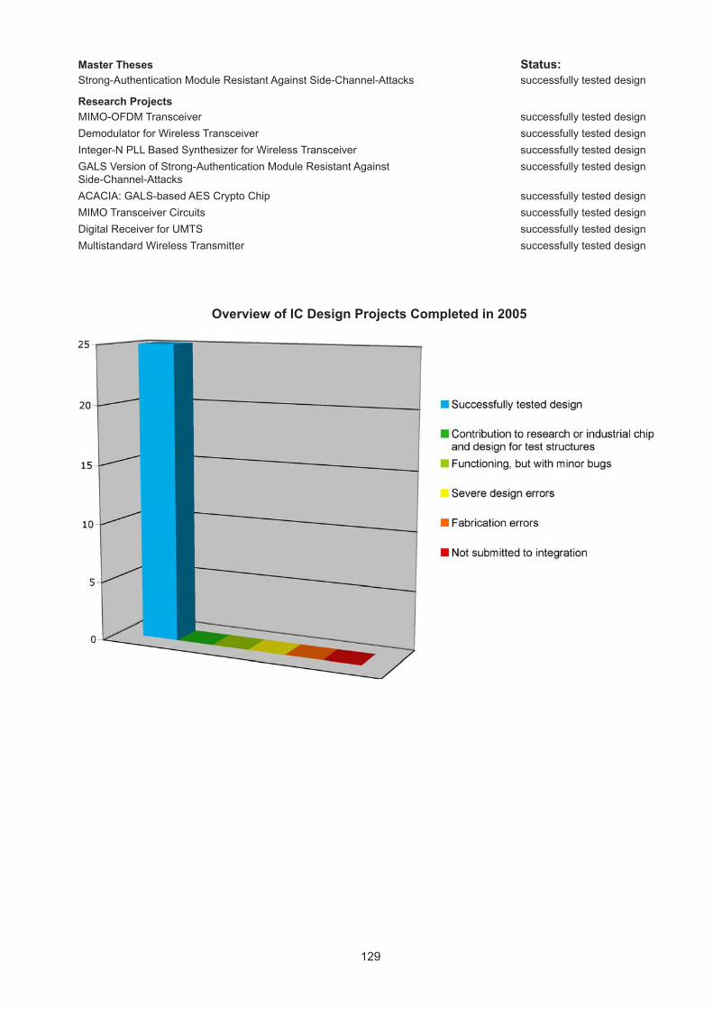
129
Master Theses Status:Strong-Authentication Module Resistant Against Side-Channel-Attacks successfully tested design
Research Projects
MIMO-OFDM Transceiver successfully tested design
Demodulator for Wireless Transceiver successfully tested design
Integer-N PLL Based Synthesizer for Wireless Transceiver successfully tested design
GALS Version of Strong-Authentication Module Resistant Against successfully tested design Side-Channel-Attacks
ACACIA: GALS-based AES Crypto Chip successfully tested design
MIMO Transceiver Circuits successfully tested design
Digital Receiver for UMTS successfully tested design
Multistandard Wireless Transmitter successfully tested design
Overview of IC Design Projects Completed in 2005

130
IC and System Design and Test
Subject: Real-Time MIMO OFDM Systems for High Speed Broadband Wireless Access
Partners: Communication Technology Laboratory, ETH Zürich, Zürich (Switzerland)Period: July 02 – June 05Funding, Number: ETH Zürich, Zürich (Switzerland), TH-6 02-2
Subject: Micropower Circuits for Digital Hearing Aids
Partners: Bernafon AG, Bern (Switzerland)Period: November 03 – October 05Funding, Number: KTI*, 6695.2 NMS Bernafon AG, Bern (Switzerland)
Subject: Multi-standard Software Defined Radio for Multimedia Applications
Partners: BridgeCo AG, Dübendorf (Switzerland) Computer Engineering and Networks Laboratory, ETH Zürich, Zürich (Switzerland)Period: March 05 – August 06Funding, Number: KTI*, 7641.1 NMPP BridgeCo AG, Dübendorf (Switzerland)
Analog and Mixed-Signal Design
Subject: CMOS (SOI) for Low Power RF Wireless
Partners: ACP AG, Zürich (Switzerland)Period: January 03 – December 05Funding, Number: KTI*, 6148.1 NMS
Subject: CITE – Critical Circuit Technologies for Flexible Mobile Receivers
Partners: Philips Zürich AG Semiconductors, Zürich (Switzerland)Period: July 03 – June 06Funding, Number: KTI*, 6171.2 NMS
Subject: OREMO – Optimized Receivers for Mobile Communications
Partners: ACP AG, Zürich (Switzerland)Period: December 03 – December 06Funding, Number: KTI*, 6767.1 NMS ACP AG, Zürich (Switzerland)
Technology CAD
Subject: Large Scale Eigenvalue Problems in Opto-Electronic Semiconductor Lasers and Accelerator Cavities
Partners: Institute for Scientific Computing, ETH Zürich, Zürich (Switzerland) Department of Computer Science, University Basel, Basel (Switzerland) Paul Scherrer Institute, Villigen (Switzerland)Period: January 2003 – February 2005Funding, Number: “Strategic Excellence Projects” (SEP): Computational Science and Engineering (CSE) ETH Zürich, TH-1 02-4
Subject: Large and Small Signal Analysis Methods for Physical Semiconductor Devices – Harmonic Balance and Optical AC Analysis (LASSIS)
Partners: Synopsys Switzerland LLC, Zürich (Switzerland)Period: June 03 – May 06Funding, Number: KTI*, 6378.1 NMS Synopsys Switzerland LLC, Zürich (Switzerland)
Subject: Parametric Design and Analysis for Semiconductor Technology Computer Aided Design (PARA – TCAD)
Partners: Synopsys Switzerland LLC, Zürich (Switzerland)Period: November 03 – May 0Funding, Number: KTI*, 6650.2 NMS Synopsys Switzerland LLC, Zürich (Switzerland)
Research Projects – Overview
131
Subject: Raise of Active n-Dopant Concentration in Silicon by Codoping (CODOPING)
Period: October 04 – September 06Funding, Number: SNF*, 200021-105414
Subject: Analysis and Simulation of SOI MOSFET Semiconductor Technology
Partners: Fujitsu Laboratories Ltd., Tokyo (Japan)Period: October 02 – March 06Funding, Number: Fujitsu Laboratories Europe, Hayes (UK), -
Subject: Bauelementesimulation von ESD Schutzelementen (Device Simulation of ESD Protection Elements)
Partners: Infineon Technologies AG, München (Germany)Period: October 03 – March 05Funding, Number: Infineon Technologies AG, München (Germany),
Subject: Robust iterative solvers for linear systems in nanoelectronic computational science (ROBUST)
Period: April 05 – March 07Funding, Number: SNF*, 200021-107945-1
Subject: SUGERT – Strategic User Group for European Research on TCAD (European IST Project)
Partners: SUGERT ConsortiumPeriod: February 05 – January 08Funding, Number: European Union, IST-03-15995
Subject: Non Equilibrium Quantum Transport in Semiconsuctor Nanostructures: Bridging the Ballistic and Dissipative Regimes (NEQUATTRO)
Period: October 05 – September 07
Funding, Number: SNF*, 200021-109393-1
Computational Optoelectronics
Subject: Simulation and Design of High Performance Semiconductor Optical Amplifiers and Superluminescent Light Emitting Diodes (SOA – SLED)
Partners: Exalos AG, Zürich (Switzerland) Synopsys Switzerland LLC, Zürich (Switzerland)Period: November 03 – October 06Funding, Number: KTI*, 6429.1 NMS Synopsys Switzerland LLC, Zürich (Switzerland)
Subject: High Speed and Quantum-Well Photodetectors
Partners: Albis Optoelectronics AG, Zürich (Switzerland) Synopsys Switzerland LLC, Zürich (Switzerland)Period: June 02 – Mai 05Funding, Number: TOP NANO 21, 5782.1 TNS Synopsys Switzerland LLC, Zürich (Switzerland)
Subject: Modeling of General Multi-Quantum-Well Structures Including Self-Consistent Coupling to a Laser Simulator (MQW)
Partners: Bookham (Schweiz) AG, Zürich (Switzerland) Synopsys Switzerland LLC, Zürich (Switzerland)Period: January 02 – March 05Funding, Number: TOP NANO 21, 5785.1 TNS Synopsys Switzerland LLC, Zürich (Switzerland)
Subject: TCAD Based Optimization of Vertical-Cavity Surface-Emittting Lasers (VCSEL-TCAD)
Partners: Laboratory of Physics of Nanostructures, EPF Lausanne, Lausanne (Switzerland) Avalon Photonics Ltd., Zürich (Switzerland) Beam Express S.A., Lausanne (Switzerland) Synopsys Switzerland LLC, Zürich (Switzerland)Period: June 04 – Mai 06Funding, Number: KTI*, 6941.2 NMS-NM Avalon Photonics Ltd., Zürich (Switzerland) Synopsys Switzerland LLC, Zürich (Switzerland) Beam Express S.A., Lausanne (Switzerland)
132
Subject: Microscopic Investigation of Optical Properties in Quantized Semiconductors Structures (GAIN)
Period: April 05 – March 08Funding, Number: SNF*, 200021-107932
Subject: Correct Wavelength-Scale Computer Simulation of Resonant Cavity Light-Emmitting Diodes as High Efficiency Light Sources (SERCLED)
Partners: Fiber Optics Communication Laboratory, State Engineering University of Armenia, Yerevan (Armenia)Period: October 05 – September 08Funding, Number: SNF*, SCOPES IB7320-111057-1
Subject: Design and Fabrication of Electrically Pumped Ultrafast Vertical-Extzernal Cavity Laser using Physics-based Simulation (E-VECSEL)
Partners: Institute for Quantum Electronics, ETH Zürich, Zürich (Switzerland)Period: October 05 - September 08
Funding, Number: ETH Zürich, Zürich (Switzerland), TH-46/ 05-02
Subject: Photonic Vrystal Purcell-Light Emitters: Model and Fabrication (PHOTONICS)
Partners: Institute for Quantum Electronics and Photonics, EPF Lausanne, Lausanne (Switzerland)Period: November 05 – October 07
Funding, Number: SER*, COST C05.0070
Physical Characterization and Technology Development
Subject: SINANO – Silicon-Based Nanodevices (European IST Project)
Partners: SINANO ConsortiumPeriod: January 04 - December 06Funding, Number: BBW*, European Union, IST-2002-506844
Subject: PORTES – Power Reliability for Traction Electronics (European MC Project)
Partners: PORTES ConsortiumPeriod: February 05 - January 08
Funding, Number: European Union, MTKI-CT-2004-517224
Bio Electromagnetics and Electromagnetic Compatibility
Subject: ULTRACOM: Channel Model of the Human Body for Medical Monitoring Systems
Partners: Miromico AG, Zürich (Switzerland) Foundation for Research on Information Technologies in Society (IT’IS), Zürich (Switzerland) University Hospital, University Bern, Bern (Switzerland)Period: October 03 – March 05 KTI*, 6454.3 NMS Miromico AG, Zürich (Switzerland)
Subject: Optical Link FR-Field Sensor for Time and Frequency Domain Measurements (TDS)
Partners: Foundation for Research on Information Technologies in Society (IT’IS), Zürich (Switzerland) Schmid & Partner Engineering AG, Zürich (Switzerland)Period: September 04 – August 06Funding, Number: KTI*, 7146.2 NMPP-NM Schmid & Partner Engineering AG, Zürich (Switzerland)
Subject: Forschungskooperation IT’IS – ETH Zürich (Research Cooperation IT’IS – ETH Zürich)
Partners: Foundation for Research on Information Technologies in Society (IT’IS), Zürich (Switzerland)Period: since January 00Funding, Number: IT’IS, Zürich (Switzerland), -
AbbreviationsBBT Federal Office for Professional Education and Technology (a Swiss Government Agency)BBW Federal Office for Education and Science (a Swiss Government Agency)KTI Commission for Technology and Innovation (a Swiss Government Agency)SER State Secretariat for Education and Research (a Swiss Government Agency)SNF Swiss National Science FoundationTOP NANO 21 Technology Oriented Program for Nano Sciences (Research and Technical Development Cooperations funded by the Swiss Government)
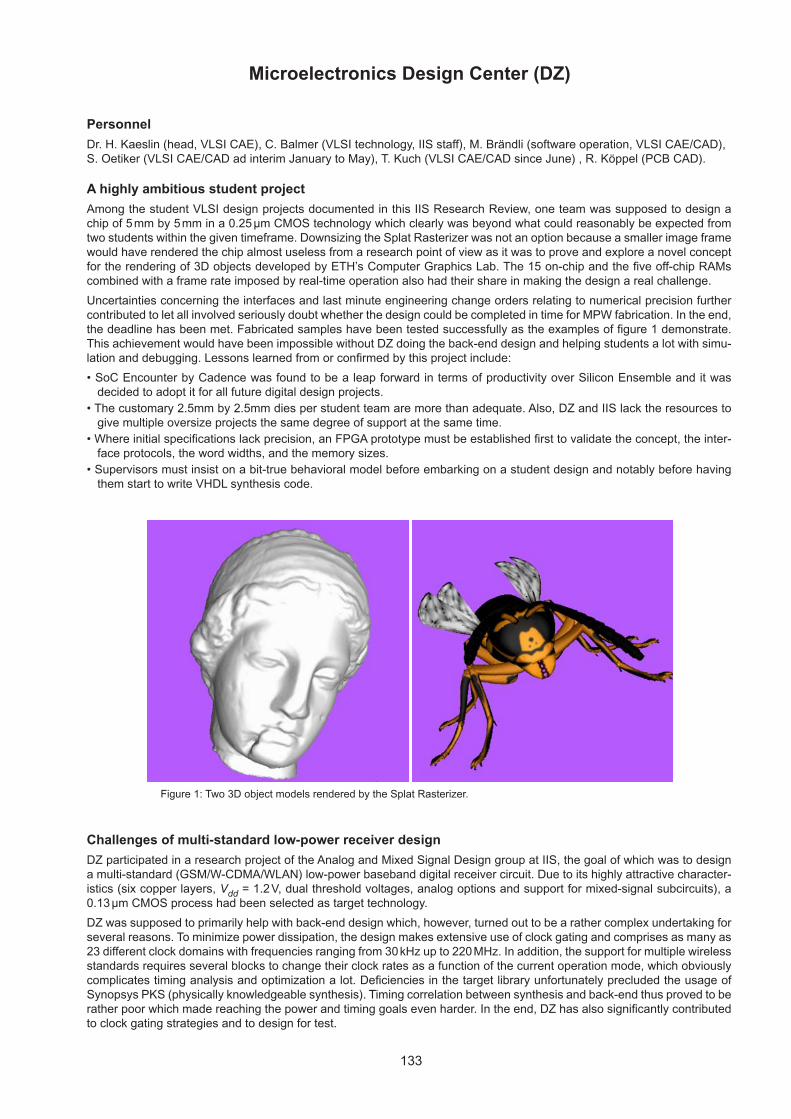
133
Personnel
Dr. H. Kaeslin (head, VLSI CAE), C. Balmer (VLSI technology, IIS staff), M. Brändli (software operation, VLSI CAE/CAD), S. Oetiker (VLSI CAE/CAD ad interim January to May), T. Kuch (VLSI CAE/CAD since June) , R. Köppel (PCB CAD).
A highly ambitious student project
Among the student VLSI design projects documented in this IIS Research Review, one team was supposed to design a chip of 5 mm by 5 mm in a 0.25 µm CMOS technology which clearly was beyond what could reasonably be expected from two students within the given timeframe. Downsizing the Splat Rasterizer was not an option because a smaller image frame would have rendered the chip almost useless from a research point of view as it was to prove and explore a novel concept for the rendering of 3D objects developed by ETH’s Computer Graphics Lab. The 15 on-chip and the five off-chip RAMs combined with a frame rate imposed by real-time operation also had their share in making the design a real challenge.
Uncertainties concerning the interfaces and last minute engineering change orders relating to numerical precision further contributed to let all involved seriously doubt whether the design could be completed in time for MPW fabrication. In the end, the deadline has been met. Fabricated samples have been tested successfully as the examples of figure 1 demonstrate. This achievement would have been impossible without DZ doing the back-end design and helping students a lot with simu-lation and debugging. Lessons learned from or confirmed by this project include:
• SoC Encounter by Cadence was found to be a leap forward in terms of productivity over Silicon Ensemble and it was decided to adopt it for all future digital design projects.
• The customary 2.5mm by 2.5mm dies per student team are more than adequate. Also, DZ and IIS lack the resources to give multiple oversize projects the same degree of support at the same time.
• Where initial specifications lack precision, an FPGA prototype must be established first to validate the concept, the inter-face protocols, the word widths, and the memory sizes.
• Supervisors must insist on a bit-true behavioral model before embarking on a student design and notably before having them start to write VHDL synthesis code.
Challenges of multi-standard low-power receiver design
DZ participated in a research project of the Analog and Mixed Signal Design group at IIS, the goal of which was to design a multi-standard (GSM/W-CDMA/WLAN) low-power baseband digital receiver circuit. Due to its highly attractive character-istics (six copper layers, Vdd = 1.2 V, dual threshold voltages, analog options and support for mixed-signal subcircuits), a 0.13 µm CMOS process had been selected as target technology.
DZ was supposed to primarily help with back-end design which, however, turned out to be a rather complex undertaking for several reasons. To minimize power dissipation, the design makes extensive use of clock gating and comprises as many as 23 different clock domains with frequencies ranging from 30 kHz up to 220 MHz. In addition, the support for multiple wireless standards requires several blocks to change their clock rates as a function of the current operation mode, which obviously complicates timing analysis and optimization a lot. Deficiencies in the target library unfortunately precluded the usage of Synopsys PKS (physically knowledgeable synthesis). Timing correlation between synthesis and back-end thus proved to be rather poor which made reaching the power and timing goals even harder. In the end, DZ has also significantly contributed to clock gating strategies and to design for test.
Microelectronics Design Center (DZ)
Figure 1: Two 3D object models rendered by the Splat Rasterizer.
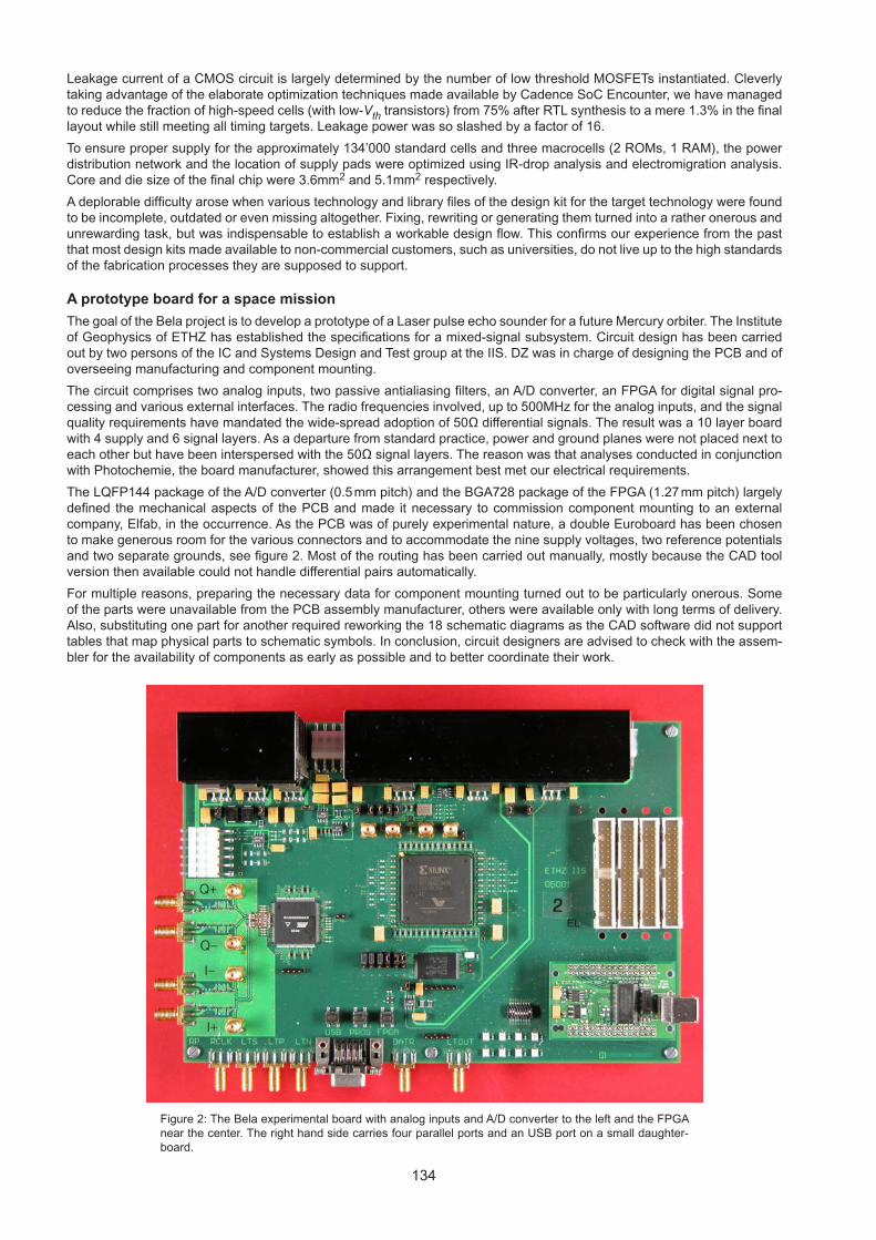
134
Leakage current of a CMOS circuit is largely determined by the number of low threshold MOSFETs instantiated. Cleverly taking advantage of the elaborate optimization techniques made available by Cadence SoC Encounter, we have managed to reduce the fraction of high-speed cells (with low-Vth transistors) from 75% after RTL synthesis to a mere 1.3% in the final layout while still meeting all timing targets. Leakage power was so slashed by a factor of 16.
To ensure proper supply for the approximately 134’000 standard cells and three macrocells (2 ROMs, 1 RAM), the power distribution network and the location of supply pads were optimized using IR-drop analysis and electromigration analysis. Core and die size of the final chip were 3.6mm2 and 5.1mm2 respectively.
A deplorable difficulty arose when various technology and library files of the design kit for the target technology were found to be incomplete, outdated or even missing altogether. Fixing, rewriting or generating them turned into a rather onerous and unrewarding task, but was indispensable to establish a workable design flow. This confirms our experience from the past that most design kits made available to non-commercial customers, such as universities, do not live up to the high standards of the fabrication processes they are supposed to support.
A prototype board for a space mission
The goal of the Bela project is to develop a prototype of a Laser pulse echo sounder for a future Mercury orbiter. The Institute of Geophysics of ETHZ has established the specifications for a mixed-signal subsystem. Circuit design has been carried out by two persons of the IC and Systems Design and Test group at the IIS. DZ was in charge of designing the PCB and of overseeing manufacturing and component mounting.
The circuit comprises two analog inputs, two passive antialiasing filters, an A/D converter, an FPGA for digital signal pro-cessing and various external interfaces. The radio frequencies involved, up to 500MHz for the analog inputs, and the signal quality requirements have mandated the wide-spread adoption of 50Ω differential signals. The result was a 10 layer board with 4 supply and 6 signal layers. As a departure from standard practice, power and ground planes were not placed next to each other but have been interspersed with the 50Ω signal layers. The reason was that analyses conducted in conjunction with Photochemie, the board manufacturer, showed this arrangement best met our electrical requirements.
The LQFP144 package of the A/D converter (0.5 mm pitch) and the BGA728 package of the FPGA (1.27 mm pitch) largely defined the mechanical aspects of the PCB and made it necessary to commission component mounting to an external company, Elfab, in the occurrence. As the PCB was of purely experimental nature, a double Euroboard has been chosen to make generous room for the various connectors and to accommodate the nine supply voltages, two reference potentials and two separate grounds, see figure 2. Most of the routing has been carried out manually, mostly because the CAD tool version then available could not handle differential pairs automatically.
For multiple reasons, preparing the necessary data for component mounting turned out to be particularly onerous. Some of the parts were unavailable from the PCB assembly manufacturer, others were available only with long terms of delivery. Also, substituting one part for another required reworking the 18 schematic diagrams as the CAD software did not support tables that map physical parts to schematic symbols. In conclusion, circuit designers are advised to check with the assem-bler for the availability of components as early as possible and to better coordinate their work.
Figure 2: The Bela experimental board with analog inputs and A/D converter to the left and the FPGA near the center. The right hand side carries four parallel ports and an USB port on a small daughter-board.
135
Supported fabrication processes
As any list of fabrication processes and libraries would be outdated by the time it gets printed, we kindly ask prospective users to refer to our documentation on the Intranet available at www.dz.ee.ethz.ch/support/ic/technologies.
Design Activities
A statistical overview of all IC design activities conducted in 2005 with the EDA installations operated by DZ is given in the table below along with the laboratory involved and other technical information.
IC Design Teaching Research Total
Process family Foundry IIS ISI IfE IQE
250 nm CMOS 180 nm CMOS 180 nm BiCMOS 130 nm CMOS 0.6 mm CMOS First Lab MLLD2005
UMC UMC IBM STM X_FAB IfE
10 - - - - -
- 4 - 9 - -
- - 1 - - -
- - - - -
run
- - - - 4 -
10 4 1 9 4
run
Total 10 13 1 run 4 47
Courses
Schematic Entry and Physical Layout for PCBs
Organized by: Microelectronics Design CenterTrainers: R. KöppelDates: 6 days from April 13 to May 2, 2005Participants: 3
Schematic Entry and Physical Layout for PCBs
Organized by: Microelectronics Design CenterTrainers: R. KöppelDates: 4 days from November 10 to December 1, 2005Participants: 8

136
Profile
The IT’IS Foundation was established on November 15th, 1999 through the initiative and support of the Swiss Fed-eral Institute of Technology in Zurich (ETHZ), the global wireless communications industry, and several govern-mental agencies. IT’IS stands for Information Technolo-gies in Society.
The aim of IT’IS is to create a flexible and dynamic re-search institution capable of addressing the research needs of society in the explosively expanding field of in-formation technologies. Some of the areas encompassed are:
• evaluation of the safety and risks related to current and emerging information technologies
• exploration of information technologies for medical, di-agnostic, and life support systems
• improvement of the accessibility of information tech-nologies for all members of society including disabled persons.
IT’IS is committed to the advancement of science for the benefit of society at large and to maintaining strict inde-pendence from any particular interest groups. These prin-ciples are reflected in the Foundation’s charter as well as the balance of the composition of its board, with distin-guished personalities from science, the public sector, and the global wireless communications industry. IT’IS is a non-profit tax-exempt research organization.
Infrastructure and Cooperation
During the start-up phase of the Foundation, not only the main office but also the research units and laboratories were located at ETH Zurich. In April 2000, IT’IS opened jointly with Schmid & Partner Engineering AG one of the world’s finest near-field laboratories in downtown Zurich. In 2003, the IT’IS facilities at Zeughausstrasse 43 were more than doubled, including two new laboratories (a large semi-anechonic chamber for general near-field and dosimetric measurements and a reverberation chamber for EMI and other tests) to address new challenges in the area of health support systems.
The closest and most important cooperative ties of IT’IS are with the Integrated Systems Laboratory and other laboratories of ETH Zurich. In addition, the IT’IS team has substantial experience in multidisciplinary cooperation through a multitude of projects, resulting in an interna-tional network of over 50 academic and industry research partners in Europe, the USA, and Asia.
Current Research Focus
The current research focus of IT’IS lies in the three areas 1) sensing and computational techniques for electromag-netic analysis, 2) health risk assessment, and 3) health support systems. In addition, IT’IS offers various services to governments and industry, including antenna engineer-ing, device optimization for operation in EMF hostile en-vironments, testing of compliance, and safety white pa-pers.
The first area, Sensing and Computational Techniques, consists of several projects, ranging from new sensor
technologies and new measurement procedures for test-ing the compliance of wireless devices and base stations with safety limits to extensions and improvements of FDTD for near-field applications and optics.
The second research area is Health Risk Assessment. This mainly involves the development, provision, and maintenance of exposure setups as well as the provision of detailed dosimetry for more than thirty experiments con-ducted in cooperation with biological and medical research groups in Switzerland, Europe, USA, China, and Japan. These include in vitro, in vivo, and human provocation studies at different mobile communications bands as well as some ELF experiments. In addition, IT’IS is conducting basic and review studies for different agencies.
The Health Support System group, formed in 2003, is de-veloping rapidly. Of particular mention are in-house proj-ects supporting the development of hyperthermia planning tools for the treatment of cancerous tumors, controllable nerve stimulation for neuroprothysis, optimized signal transmission over the body, and antenna designs for on-body and implanted antennas.
In addition to providing research results for governmen-tal agencies through participation in standardization bod-ies and providing consultation to governments, IT’IS also provides courses to members of the public, industry, and universities.
Current research projects are being supported by public funds such as those of NIEHS, the Quality of Life Pro-gramme of the European Union, EUREKA, KTI, VERUM Foundation, health agencies such as BAG and BfS, as well as other governmental institutions. Funding from in-dustry comes from major mobile communications manu-facturers and service providers as well as from smaller companies.
Director
Prof. Dr. Niels Kuster
Main Office Address Mailing Address and Labs
IT’IS Foundation IT’IS Foundation
ETH Zentrum ETZ Zeughausstrasse 43
CH-8092 Zurich CH-8004 Zurich
Switzerland Switzerland
Phone: +41 44 245 9696 [email protected]
Fax: +41 4 245 9699
w w w. i t i s . e t h z . c h
Joint Research Cooperation with the IT’IS Foundation
137
IC and System Design and Test[D1] A. Burg, M. Borgmann, M. Wenk, M. Zellweger, W. Fichtner, H. Bölcskei
VLSI Implementation of MIMO Detection Using the Sphere Decoding Algorithm, IEEE Journal of Solid-State Circuits, vol. 40, no. 7, pp. 1566-1577, Jul 2005
[D2] A. Burg, S. Häne, D. Perels, P. Lüthi, N. Felber, W. Fichtner Receiver Design for Multi-Antenna Wireless Communications, Proc. of IEEE Conf. on Research in Microelectronics (PRIME 2005), Lausanne, Switzerland, vol. 2, pp. 35-38, Jul 2005
[D3] A. Burg, M. Rupp Demonstrators and Testbeds, Smart Antennas - State-of-the-Art, EURASIP Book Series Journals, Jan 2005
[D4] F. Carbognani, F. Bürgin, N. Felber, H. Kaeslin, W. Fichtner Two-Phase Clocking and a New Latch Design for Low-Power Portable Applications, Proc. of International Workshop on Power and Timing Modeling, Optimization and Simulation, Leuven, Belgium, vol. 3728, pp. 446-455, Sep 2005
[D5] F. Carbognani, F. Bürgin, N. Felber, H. Kaeslin, W. Fichtner A 2.7-μW/MHz Transmission-Gate-Based 16-bit Multiplier for Digital Hearing Aids, Proc. of Midwest Symposium on Circuits and Systems (MWSCAS), Cincinnati, Ohio, USA, Aug 2005
[D6] F. Carbognani, F. Bürgin, L. Henzen, H. Koch, H. Magdassian, C. Pedretti, H. Kaeslin, N. Felber, W. Fichtner A 0.67-mm2 45-μW DSP VLSI Implementation of an Adaptive Directional Microphone for Hearing Aids, Proc. of European Conference on Circuit Theory and Design (ECCTD), Cork, Ireland, vol. 3, pp. 141-144, Aug 2005
[D7] F.K. Gürkaynak, N. Felber, H. Kaeslin, W. Fichtner Area, Throughput and Security Considerations for AES Crypto-ASICs, Proc. of IEEE PhD Research in Microelectronics and Electronics, PRIME2005, Lausanne, Switzerland, Jul 2005
[D8] F.K. Gürkaynak, S. Oetiker, H. Kaeslin, N. Felber, W. Fichtner Design Challenges for a Differential Power Analysis Aware GALS based AES Crypto-ASIC, Proc. of Second International Workshop on Formal Methods for Globally-Asynchronous Locally-Synchronous Design, FMGALS2005, Verona, Italy, Jul 2005
[D9] F.K. Gürkaynak, S. Oetiker, H. Kaeslin, N. Felber, W. Fichtner Improving DPA Security by Using Globally-Asynchronous Locally-Synchronous Systems, Proc. of ESSCIRC 2005 31st European Solid-State Circuits Conference, Grenoble, France, pp. 407-410, Sep 2005
[D10] S. Häne, A. Burg, D. Perels, P. Lüthi, N. Felber, W. Fichtner FPGA Implementation of Viterbi Decoders for MIMO-BICM, Proc. of 39th Asilomar Conference on Signals, Systems, and Computers, Monterey, CA, USA, Oct 2005
[D11] D. Perels, S. Häne, P. Lüthi, A. Burg, N. Felber, W. Fichtner, H. Bölcskei ASIC Implementation of a MIMO-OFDM Transceiver for 192 Mbps WLANs, Proc. of European Solid-State Circuits Conference (ESSCIRC), Grenoble, France, pp. 215-218, Sep 2005
[D12] M. Wegmüller, A. Lehner, J. Fröhlich, R. Reutemann, M. Oberle, N. Felber, N. Kuster, O. Hess, W. Fichtner Measurement System for the Characterization of the Human Body as a Communication Channel at Low Frequency, Proc. of the 27th Annual International Conference of the IEEE Engineering in Medicine and Biology Society EMBC, Shanghai, China, Sep 2005
Analog and Mixed-Signal Design[A1] T. Burger, M. Halimic, L. Maurer, S. Mende, H. Seidel, N. Syed, B. Steinke, S. Walter
E2R Deliverable D4.3: Functional Physical Layer Architecture, http://e2r.motlabs.com/Deliverables/E2R_WP4_D4.3_050103.pdf, pp. 1-99, Jan 2005
[A2] X. Chen, Q. Huang A 9.5mW 4GHz WCDMA Frequency Synthesizer in 0.13μm CMOS, Proc. of 2005 International Symposium on Low Power Electronics and Design, San Diego, California, USA, pp. 66-71, Aug 2005
[A3] L. Maurer, T. Burger, T. Dellsperger, R. Stuhlberger, G. Hüber, M. Schmidt, R. Weigel A Digital Front-End Supported Frequency Agile Multi-Standard Wireless Receiver, FREQUENZ (Schiele&Schön), vol. 59, no. 1, pp. 3-10, Jan 2005
Publications
138
[A4] L. Maurer, T. Burger, T. Dellsperger, R. Stuhlberger, G. Hüber, M. Schmidt, R. Weigel On the Architectural Design of Frequency-Agile Multi-Standard Wireless Receivers, Proc. of 14th IST Mobile & Wireless Communications Summit, Dresden, Germany, Jun 2005
Technology CAD[T1] P.P. Altermatt, A. Schenk, B. Schmithüsen, G. Heiser
Impact of Incomplete Ionisation on Measurements of Sheet Resistivity and of Carrier Mobility in c-Si Solar Cells at Room Temperature, Proc. of 20th European Photovoltaic Conference, Barcelona, Spain, Jun 2005
[T2] M. Aschwanden, W. Philipp, K. Hess, S. Barraza-Lopez, G. Adenier Local Time Dependent Instruction-Set Model for the Experiment of Pan et al., Proc. of AIP Conference, Vaxjo, Sweden, vol. 810, no. 1, pp. 437-446, Jun 2005
[T3] N. Braga, R. Mickevicius, W. Fichtner, R. Gaska, M. S. Shur, G. Simin, and M. Asif Khan Simulation of AlGaN/GaN Heterostructure Field Effect Transistors, Proc. of 2005 International Conference on Solid State Devices and Materials, Kobe, Japan, Sep 2005
[T4] N. Braga, R. Mickevicius, V. S. Rao, W. Fichtner, R. Gaska, and M. S. Shur Non-uniform Stress Effects in GaN-based Heterojunction Field Effect Transistors, Proc. of 27th IEEE Compound Semiconductor IC Symposium, Palm Springs, CA , USA, Nov 2005
[T5] S.C. Brugger, A. Schenk First-Principle Computation of Relaxation Times in Semiconductors for Low and High Electric Fields, Proc. of International Conference on Simulation of Semiconductor Processes and Devices SISPAD, Tokyo, Japan, pp. 151-154, Sep 2005
[T6] F.M. Bufler, A. Schenk On the Tunneling Energy within the Full-Band Structure Approach, Proc. of International Conference on Simulation of Semiconductor Processes and Devices SISPAD, Tokyo, Japan,International Conference on Simulation of Semiconductor Processes and Devices SISPAD, Tokyo, Japan,Simulation of Semiconductor Processes and Devices SISPAD, Tokyo, Japan, pp. 155-158, Sep 2005
[T7] F.M. Bufler, A. Schenk On the Tunneling Energy within the Full-Band Structure Approach, Proc. of International Conference on Simulation of Semiconductor Processes and Devices SISPAD, Tokyo, Japan, pp. 155-158, Sep 2005
[T8] J. Lorenz, D. Aemmer, D.C. Müller et al. International Technology Roadmap for Semiconductors ITRS, 2005 Edition, chapter Modeling and Simulation, Semiconductor Industry Association, San Jose, USA, 2005
[T9] D.C. Müller Deactivation and Activation of Donors in Silicon, PhD Thesis ETH-No. 15786, Hartung-Gorre Printing House, Konstanz, Germany, 2005
[T10] D.C. Müller, W. Fichtner Donor Deactivating Mechanisms and Codoping Strategies in Heavily Doped Silicon, Proc. of MRS Spring Meeting 2005, San Francisco, California, USA, Mar 2005
[T11] B. Polsky, O. Penzin, K.E. Sayed, A. Schenk, A. Wettstein, W. Fichtner On Negative Differential Resistance in Hydrodynamic Simulation of Partially Depleted SOI Transistors, IEEE Transactions on Electron Devices, vol. 52, no. 4, pp. 500-506, Apr 2005
[T12] S. Röllin Parallel Iterative Solvers in Computational Electronics, PhD Thesis ETH-No. 15859, Hartung-Gorre Printing House, Konstanz, Germany, 2005
[T13] S. Röllin, O. Schenk Maximum-Weighted Matching Strategies and the Application to Symmetric Indefinite Systems, Lecture Notes in Computer Science, vol. 3732, pp. 808-817, Dez 2005
[T14] B. Sahli, W. Fichtner Ab Initio Molecular Dynamics Simulation of Self-Interstitial Diffusion in Silicon, Physical Review B, vol. 72, no. 24, pp. 245210, Dez 2005
[T15] A. Schenk, F.O. Heinz, B. Schmithüsen DGSOI Versus Bulk: A Quantum-Ballistic Study of 25 nm nMOSFETs, Proc. of International Conference on Simulation of Semiconductor Processes and Devices SISPAD, Tokyo, Japan,International Conference on Simulation of Semiconductor Processes and Devices SISPAD, Tokyo, Japan,Simulation of Semiconductor Processes and Devices SISPAD, Tokyo, Japan, pp. 47-50, Sep 2005
Computational Optoelectronics[O1] B. Hangartner, J. Piprek, S. Odermatt, M. Streiff, B. Witzigmann
Internal Device Physics of 1.3-Micron VCSELs, Proc. of Photonics West’05, San Jose, CA, USA, vol. 5737, pp. 132-141, Jan 2005
139
[O2] B. Jacob, M. Klemenc, C. Petit, B. Witzigmann A TCAD Methodology for High-Speed Photodetectors, Solid-State Electronics, vol. 49, no. 6, pp. 1002-1008, Jun 2005
[O3] V. Laino, B. Witzigmann, M. Streiff, A. Bregy, A. Witzig, U.T. Schwarz Study of Substrate Modes in a (Al,In)GaN/SiC Semiconductor Laser Using Finite Element Approach, Proc. of 5th International Conference on Numerical Simulation of Optoelectronic Devices NUSOD, Berlin, Germany, pp. 33, Sep 2005
[O4] S. Odermatt, S. Eitel, M. Pfeiffer, A. Bregy, B. Witzigmann Physics of VCSELs: Temperature-Dependent Modulation Response, Proc. of 5th International Conference on Numerical Simulation of Optoelectronic Devices NUSOD, Berlin, Ger-many, pp. 25-26, Sep 2005
[O5] S. Odermatt, M. Luisier, B. Schmithüsen, M. Streiff, R. Hövel, B. Witzigmann Multidimensional Noise Model and Simulation of VCSEL Devices, Proc. of SPIE, Physics and Simulation of Optoelectronic Devices XIII, San Jose, CA, USA, vol. 5722, pp. 211-220, May 2005
[O6] S. Odermatt, M. Luisier, B. Witzigmann Bandstructure Calculation Using the kp Method for Arbitrary Potentials with Open Boundary Conditions, Journal of Applied Physics, vol. 97, pp. 46104-46106, Feb 2005
[O7] M. Pfeiffer Industrial-Strength Simulation of Quantum-Well Semiconductor Lasers, PhD Thesis ETH-No. 15695, Hartung-Gorre Printing House, Konstanz, Germany, 2005
[O8] L. Schneider, M. Pfeiffer, J. Piprek, A. Witzig, B. Witzigmann Sampled-Grating DBR Laser: Calibrated 3D Simulation of Tuning Characteristics, Proc. of SPIE Opto Ireland 2005, Dublin, Ireland, vol. 5825, Apr 2005
[O9] M. Streiff, W. Fichtner, A. Witzig Vertical-Cavity Surface Emitting Lasers: Single Mode Control and Self Heating Effects, Optoelectronic Devices: Advanced Simulation and Analysis, Springer, 0-387-22659-1, New York, NY, USA, pp. 452, 2005
[O10] A. Witzig, V. Laino, L. Schneider, B. Witzigmann Device Simulation and Statistical Analysis in Industrial Laser Design, Proc. of Photonics West’05, San Jose, CA, USA, vol. 5722, pp. 454-464, Jan 2005
[O11] B. Witzigmann, A. Bregy, F. Michel, S. Odermatt, R. Santschi, M. Streiff A Three-Dimensional Microscopic Simulation For Vertical Cavity Surface Emitting Lasers, Proc. of 5th International Conference on Numerical Simulation of Optoelectronic Devices NUSOD, Berlin, Ger-many, pp. 23-24, Sep 2005
[O12] B. Witzigmann, M. Streiff, S. Odermatt, M. Luisier, V. Laino, A. Witzig, D. Vez, P. Royo Comprehensive Simulation of Vertical Cavity Surface Emitting Lasers, Proc. of IWCE’2004, West Lafayette, Indiana, US, pp. 87-88, Jan 2005
[O13] B. Witzigmann, M. Streiff, S. Odermatt, M. Luisier, V. Laino, A. Witzig, D. Vez, P. Royo Comprehensive Simulation of Vertical Cavity Surface Emitting Lasers: Inclusion of a Many-Body Gain Model, Journal of Computational Electronics, vol. 4, pp. 7-10, Apr 2005
[O14] B. Witzigmann, M. Streiff, C. Zinoni, C. Monat, B. Alloing, A. Fiore Technology CAD based Design of Semiconductor Optical Microcavities for Single Photon Emitters, Proc. of SPIE Microtechnologies for the New Millennium, Sevilla, Spain, vol. 5840, pp. 602-613, May 2005
Physical Characterization[P1] M. Buzzo, M. Ciappa, W. Fichtner
2D Junction Delineation for the Failure Analysis of Silicon Carbide Devices, Proc. of IEEE 12th International Symposium on the Physical and Failure Analysis of Integrated Circuits (IPFA), Singapore, Singapore, vol. 12, pp. 105-109, Jun 2005
[P2] M. Buzzo, M. Ciappa, M. Rüb, W. Fichtner Characterization of 2D Dopant Profiles for the Design of Proton Implanted High-Voltage Superjunctions, Proc. of IEEE 12th International Symposium on the Physical and Failure Analysis of Integrated Circuits (IPFA), Singapore, Singapore, vol. 12, pp. 285-289, Jun 2005
[P3] M. Buzzo, M. Ciappa, M. Stangoni, W. Fichtner Two-dimensional Dopant Profiling and Imaging of 4H Silicon Carbide Devices by Secondary Electron Potential Contrast, Proc. of 16th European Symposium Reliability of Electronic Devices, Failure Physics and Analysis (ESREF), Arcachon, France, pp. 1499-1504, Oct 2005
[P4] M. Buzzo, M. Ciappa, M. Stangoni, W. Fichtner Two-dimensional Dopant Profiling and Imaging of 4H Silicon Carbide Devices by Secondary Electron Potential Contrast, Microelectronics Reliability, vol. 45, pp. 1499-1504, Oct 2005
140
[P5] M. Buzzo, M. Ciappa, M. Treu, W. Fichtner Advances in Two-dimensional Dopant Profiling and Imaging of 4H-SiC Devices, Proc. of Int. Conference on Silicon Carbide and Related Materials 2005 (ICSCRM), Pittsburg, USA, Sep 2005
[P6] M. Ciappa Lifetime Prediction on the Base of Mission Profiles (Invited Paper), Proc. of 16th European Symposium Reliability of Electronic Devices, Failure Physics and Analysis (ESREF), Arcachon, France, pp. 1293-1298, Oct 2005
[P7] M. Ciappa Physics of Failures and Failure Analysis of High-Power Power Devices (Invited Paper), Proc. of International ECPE Workshop on Building-in Reliability into Power Electronic Systems, Nuremberg, Germany, Jan 2005
[P8] M. Ciappa Lifetime Prediction on the Base of Mission Profiles, Microelectronics Reliability, vol. 45, pp. 1293-1298, Oct 2005
[P9] M. Ciappa, W. Fichtner, T. Kojima, Y. Yamada, Y. Nishibe Extraction of Accurate Thermal Compact Models for Fast Electro-Thermal Simulation of IGBT Modules in Hybrid Electric Vehicles, Proc. of 16th European Symposium Reliability of Electronic Devices, Failure Physics and Analysis (ESREF), Arcachon, France, pp. 1694-1699, Oct 2005
[P10] M. Ciappa, W. Fichtner, T. Kojima, Y. Yamada, Y. Nishibe Extraction of Accurate Thermal Compact Models for Fast Electro-Thermal Simulation of IGBT Modules in Hybrid Electric Vehicles, Microelectronics Reliability, vol. 45, pp. 1694-1699, Oct 2005
[P11] M. Etherton, N. Qu, J. Willemen, W. Wilkening, S. Mettler, M. Dissegna, R. Stella, L. Zullino, A. Andreini, H. Gieser, H. Wolf, W. Fichtner Study of CDM Specific Effects for a Smart Power Input Protection Structure, Journal of Microelectronics Reliability, Dec 2005
[P12] M. Etherton, W. Wilkening, S. Mettler, P. Rose, W. Fichtner Gate Dielectric Degradation in the CDM Time DoMayn, Proc. of 9. ESD-Forum, Berlin, Germany, Nov 2005
[P13] M. Etherton, J. Willemen, W. Wilkening, N. Qu, S. Mettler, W. Fichtner Verification of CDM Circuit Simulation Using an ESD Evaluation Circuit, Proc. of 27th EOS/ESD Symposium, Anaheim, CA, USA, Sep 2005
[P14] W. Fichtner, N. Braga, M. Ciappa, V. Mickevicius, M. Schenkel Progress in Technology CAD for Power Devices, Circuits and Systems (Invited Paper), Proc. of 17th IEEE International Symposium on Power Semiconductor Devices and ICs (ISPSD), Santa Barbara, CA, USA, vol. 17, pp. 1-9, Jun 2005
[P15] U. Glaser, K. Esmark, M. Streibl, C. Russ, K. Domanski, M. Ciappa, W. Fichtner SCR Operation Mode of Diode Strings for ESD Protection, EOS/ESD Symposium Proceedings, Anaheim, CA, USA, pp. 60-69, Sep 2005
[P16] T. Kojima, Y. Yamada, Y. Nishibe, M. Ciappa, W. Fichtner A Novel Compact Thermal Modeling Approach to Electro-thermal Simulation for Automotive IGBT Modules, Proc. of Int. Power Electronics Conference 2005 (IPEC-Niigata), Niigata, Japan, Apr 2005
[P17] I. Omura High Voltage MOS Device Design: Injection Enhancement and Negative Gate Capacitance, PhD Thesis ETH-No. 14049, Hartung-Gorre Printing House, Konstanz, Germany, 2005
[P18] S. Reggiani, E. Gnani, M. Rudan, G. Baccarani, C. Corvasce, D. Barlini, M. Ciappa, W. Fichtner, M. Denison, N. Jensen, G. Groos, M. Stecher Measurement and Modeling of the Electron Impact-Ionization Coefficient in Silicon Up to Very High Temperatures, IEEE Transactions on Electron Devices, vol. 52, no. 10, pp. 2290-2299, Oct 2005
[P19] M. Rudan, S. Reggiani, E. Gnani, G. Baccarani, C. Corvasce, D. Barlini, M. Ciappa, W. Fichtner, M. Denison, N. Jensen, M. Stecher, G. Groos Experimental Validation of a New Analytical Model for the Position-Dependent Hall Voltage in Semiconductor Devices, Proc. of IEEE European Solid-State Device Research Conference 2005 (ESSDERC), Grenoble, France, pp. 565-568, Sep 2005
[P20] Y. Saad, P. Pfäffli, M. Ciappa, L. Bomholt, W. Fichtner Advanced 3D Device Simulations of Flash Memories (poster presentation), Proc. of IEEE Int. Conference on Memory Technology and Design 2005 (ICMTD), Giens, France, 21-24 May 2005
[P21] M. Stangoni Scanning Probe Techniques for Dopant Profile Characterization, PhD Thesis ETH-No. 16024, Hartung-Gorre Printing House, Konstanz, Germany, 2005
141
[P22] M. Stangoni, M. Ciappa, W. Fichtner Assessment of the Analytical Capabilities of Scanning Capacitance and Scanning Spreading Resistance Microscopy Applied to Semiconductor Devices, Proc. of 16th European Symposium Reliability of Electronic Devices, Failure Physics and Analysis (ESREF), Arcachon, France, pp. 1532-1537, Oct 2005
[P23] M. Stangoni, M. Ciappa, W. Fichtner Assessment of the Analytical Capabilities of Scanning Capacitance and Scanning Spreading Resistance Microscopy Applied to Semiconductor Devices, Microelectronics Reliability, vol. 45, pp. 1532-1537, Oct 2005
Bio-Electromagnetics and Electromagnetic Compatibility[B1] S. Benkler, H. Songoro, N. Chavannes, N. Kuster
Robust and Fully Automated Conformal Mesh Generation for Complex Conformal FDTD Applications, Proc. of Poster Presentation at 2005 IEEE AP-S International Symposium and USNC / URSI National Radio Science Meeting, Washington, DC, USA, Jul 2005
[B2] S. Benkler, H. Songoro, N. Chavannes, N. Kuster Automated and Robust Conformal Mesher for Complex Conformal FDTD Applications, Proc. of Progress In Electromagnetics Research Symposium (PIERS), Hangzhou, China, Aug 2005
[B3] V. Berdiñas Torres, S. Ebert, A. Klingenböck, J. Fröhlich, N. Kuster Dosimetry and Uncertainty Assessment of PERFORM A Exposure Systems, Proc. of Bioelectromagnetics 2005, Dublin, Ireland, Jun 2005
[B4] B. Billaudel, J.C. Gröbli, A. Hoyto, N. Kuster, I. Lagroye, J. Luukkonen, J. Naarala, N. Nikoloski, G. Ruffie, J. Schuderer, M. Sokura, D. Spät, M. Taxile, B. Veyret PERFORM-B Ornithine Decarboxylase Sub-programme: Investigation on the in vitro Effects of Mobile Phone Signals Exposure on Ornithine Decarboxylase Activity, Proc. of 27th Annual Meeting of the Bioelectromagnetics Society, Dublin, Ireland, pp. 181, Jun 2005
[B5] N. Chavannes, P. Futter, R. Tay, K. Pokovic, N. Kuster Reliable Prediction of MTE Performance Under Real Usage Conditions Using FDTD, Conference Proceedings of the 18th International Conference on Applied Electromagnetics and Communications (ICECom-2005) and joint COST 284 Workshop, Dubrovnik, Croatia, pp. 573-576, Oct 2005
[B6] N. Chavannes, P. Futter, R. Tay, K. Pokovic, N. Kuster Reliable Prediction of Mobile Phone Performance for Different Daily Usage Patterns by Numerical Methods, Proc. of XXVIIIth General Assembly of International Union of Radio Science (URSI): Programme Oral Presentations, New Delhi, India, pp. 116, Oct 2005
[B7] A. Christ, N. Chavannes, N. Nikoloski, H.U. Gerber, K. Pokovic, N. Kuster A Numerical and Experimental Comparison of Human Head Phantoms for Compliance Testing of Mobile Tele-phone Equipment, Bioelectromagnetics, vol. 26, no. 2, pp. 125-137, Feb 2005
[B8] A. Christ, A. Klingenböck, N. Kuster Absorption Mechanism of Electromagnetic Energy for Body-Mounted Devices Operating Between 30 MHz to 5800 MHz, Proc. of 27th Annual Meeting of the Bioelectromagnetics Society, Dublin, Ireland, pp. 58, Jun 2005
[B9] A. Christ, A. Klingenböck, N. Kuster Energy Absorption in Layered Biological Tissue and its Consequences on the Compliance Testing of Body-Mount-ed Wireless Devices, Proc. of Progress in Electromagnetics Research Symposium (PIERS), Hangzhou, China, pp. 619, Aug 2005
[B10] A. Christ, A. Klingenböck, N. Kuster Energy Absorption in Layered Biological Tissues in the Near- and Far-Field of Antennas of Body-Mounted Devices, Proc. of XXVIIIth General Assembly of International Union of Radio Science (URSI), New Delhi, India, pp. 117, Oct 2005
[B11] A. Christ, N. Kuster Differences in RF energy absorption in the heads of adults and children, Bioelectromagnetics, vol. 26, no. S7, pp. S31-S44, Oct 2005
[B12] B. Cosquer, A.P. de Vasconcelos, J. Fröhlich, J.C. Cassel Blood-Brain Barrier and Electromagnetic Fields: Effects of Scopolamine Methylbromide on Working Memory after Whole-Body Exposure to 2.45GHz Microwaves in Rats, Behavioural Brain Research, vol. 161, no. 2, pp. 229-237, Jul 2005
[B13] B. Cosquer, R. Galani, N. Kuster, J.C. Cassel Whole-Body Exposure to 2.45 GHz Electromagnetic Fields Does not Alter Anxiety Responses in Rats: A Plus-Maze Study Including Test Validation, Behavioural Brain Research, vol. 156, no. 1, pp. 65-74, Jan 2005
142
[B14] B. Cosquer, R. Galani, A. Pereira de Vasconcelos, J. Fröhlich, N. Kuster, J.C. Cassel Whole Body Exposure to 2.45GHz Electromagnetic Fields Does not Alter Spatial Working Memory, Anxiety Responses and Blood-Brain Barrier Permeability in Rats, Proc. of 27th Annual Meeting of the Bioelectromagnetics Society, Dublin, Ireland, pp. 182, Jun 2005
[B15] B. Cosquer, N. Kuster, J.C. Cassel Whole-Body Exposure to 2.45GHz Electromagnetic Fields Does not Alter 12-Arm Radial-Maze with Reduced Access to Spatial Cues in Rats, Behavioural Brain Research, vol. 161, no. 2, pp. 331-334, Jul 2005
[B16] M. De Bruijne, T. Samaras, E. Neufeld, N. Chavannes, G. Van Rhoon Quantitative Three-Dimensional SAR Validation of the Lucite Cone Applicator, ESHO 2005 Book of Abstracts, Graz, Austria, pp. 40, Jun 2005
[B17] S. Ebert, C. Dasenbrock, T. Tillmann, N. Kuster Thermal Response and Threshold Measurements in Mice Exposed to 905 MHz, Proc. of 27th Annual Meeting of the Bioelectromagnetics Society, Dublin, Ireland, pp. 173, Jun 2005
[B18] S. Ebert, S.J. Eom, J. Schuderer, U. Apostel, T. Tillmann, C. Dasenbrock, N. Kuster Response, Thermal Regulatory Threshold, and Thermal Breakdown Threshold of Restrained RF-exposed Mice at 905 MHz, Physics in Medicine and Biology, vol. 50, no. 21, pp. 5203-5215, Nov 2005
[B19] S. Ebert, N. Nikoloski, V. Berdiñas Torres, J. Fröhlich, N. Kuster In vivo Exposure Setups for Large Scale Toxicity / Carcinogenicity Studies with Rats at 900 / 1800MHz, Abstracts of Progress in Electromagnetics Research Symposium (PIERS), Hangzhou, China, pp. 618, Aug 2005
[B20] P. Futter, N. Chavannes, R. Tay, M. Meili, A. Klingenböck, K. Pokovic, N. Kuster Reliable Prediction of Mobile Phone Performance Under Real Usage Conditions Using the FDTD Method, Proc. of the 2005 International Symposium on Antennas and Propagation (ISAP2005), Seoul, Korea, vol. 2, pp. 355-358, Jul 2005
[B21] B.D. Görlitz, M. Müller, S. Ebert, H. Hecker, N. Kuster, C. Dasenbrock Effects of 1-week and 6-week Exposure to GSM/DCS radioFrequency Radiation on Micronucleus Formation in B6C3F1 Mice, Radiation Research, vol. 164, no. 4, pp. 431-439, Oct 2005
[B22] R. Huber, V. Treyer, J. Schuderer, T. Berthold, A. Buck, N. Kuster, H.P. Landolt, P. Achermann Exposure to Pulse Modulated radioFrequency Exposure Affects Regional Cerebral Blood Flow, European Journal of Neuroscience, vol. 21, no. 4, pp. 1000, Feb 2005
[B23] N. Jones, A. Bottomley, R. Haylock, R. Saunders, N. Kuster, Z. Sienkiewicz PERFORM-B: Behavioural Studies With Mice, Proc. of 27th Annual Meeting of the Bioelectromagnetics Society, Dublin, Ireland, pp. 184, Jun 2005
[B24] W. Kainz, A. Christ, J. Chen Current and Future Needs for Computational Methods for Medical Applications, Proc. of XXVIIIth General Assembly of International Union of Radio Science (URSI): Programme Oral Presenta-tions, New Delhi, India, pp. 179, Oct 2005
[B25] W. Kainz, A. Christ, T. Kellom, S. Seidman, N. Nikoloski, B. Beard, N. Kuster Dosimetric Comparison of the Specific Anthropomorphic Mannequin (SAM) to 14 Anatomical Head Models Using a Novel Definition for the Mobile Phone Positioning, Physics in Medicine and Biology, vol. 50, pp. 3423-3445, Jul 2005
[B26] S. Kühn, A. Kramer, U. Lott, N. Kuster Assessment of Human Exposure by Electromagnetic Radiation from Wireless Devices in Home and Office Envi-ronments, Proc. of Base Stations and Wireless Networks: WHO Workshop, Geneva, Switzerland, Aug 2005
[B27] S. Kühn, N. Kuster Instrumentation for Experimental Dosimetry and How to Apply It Correctly, Proc. of EMF Health Risk Research Lessons Learned and Recommendations for the Future, Ascona, Switzerland, Mar 2006
[B28] M.A. Kelsh, C. Sulser, M. Shum, M. McNeely, N. Kuster, J. Fröhlich, A. Sheppard Evaluation of Mobile Phone Handset Exposures Using Software Modified Phones and Field Phantom Systems, Proc. of 27th Annual Meeting of the Bioelectromagnetics Society, Dublin, Ireland, pp. 139, Jun 2005
[B29] S. Kühn, A. Kramer, U. Lott, N. Kuster Assessment Methods for Demonstrating Compliance with Safety Limits of Wireless Devices Used in Home and Office Environments, Proc. of URSI General Assembly 2005, Delhi, India, Oct 2005
[B30] S. Kühn, A. Kramer, U. Lott, N. Kuster Assessment of Human Exposure by Electromagnetic Radiation from Wireless Devices in Home and Office Environment, Proc. of Bioelectromagnetics 2005, Dublin, Ireland, Jun 2005
143
[B31] S. Kühn, C. Sulser, N. Kuster Assessment Technique for the Cumulative Exposure of Mobile Phones in Real Networks, Proc. of URSI General Assembly 2005, Delhi, India, Oct 2005
[B32] G. Neubauer, M. Röösli, M. Feychting, Y. Hamnerius, L. Kheifets, N. Kuster, I. Ruiz, J. Schüz, J. Wiart Feasibility of Future Epidemiological Studies on Possible Health Effects of Mobile Phone Base Stations, Proc. of 27th Annual Meeting of the Bioelectromagnetics Society, Dublin, Ireland, pp. 102, Jun 2005
[B33] E. Neufeld, T. Samaras, N. Chavannes, N. Kuster Important Aspects of Electromagnetic Modeling in Hyperthermia Treatment Planning, Bioelectromagnetics 2005 Abstract Collection, Dublin, Ireland, Jun 2005
[B34] E. Neufeld, T. Samaras, N. Chavannes, N. Kuster Important Aspects of Electromagnetic Modeling in Hyperthermia Treatment Planning Using Non-Uniform FDTD, ESHO 2005 Book of Abstracts, Graz, Austria, Jun 2005
[B35] E. Neufeld, T. Samaras, N. Chavannes, N. Kuster Robust Medical Image Segmentation for Hyperthermia Treatment Planning, ESHO 2005 Book of Abstracts, Graz, Austria, Jun 2005
[B36] N. Nikoloski, J. Fröhlich, T. Samaras, J. Schuderer, N. Kuster Reevaluation and Improved Design of the TEM Cell In Vitro Exposure Unit for Replication Studies, Bioelectromagnetics, vol. 26, no. 3, pp. 215-224, Apr 2005
[B37] T. Nikolova, J. Czyz, A. Rolletschek, P. Blyszczuk, J. Fuchs, G. Jovtchev, J. Schuderer, N. Kuster, A.M. Wobus Electromagnetic fields affect transcript levels of apoptosis-related genes in embryonic stem cell-derived neural progenitor cells, FASEB J, vol. 19, no. 12, pp. 1686-1688, Aug 2005
[B38] K. Pokovic, N. Nikoloski, A. Christ, N. Kuster Compliance Testing Tools and Procedures for Emerging Technologies (3-6GHz), Proc. of 18th International Conference on Applied Electromagnetics and Communications (ICECom-2005) and joint COST 284 Workshop, Dubrovnik, Croatia, pp. 577-580, Oct 2005
[B39] T. Samaras, A. Christ, N. Kuster On the Worst Case Temperature Rise in a One-Dimensional Tissue Model Exposed to RadioFrequency Radiation, Proc. of XXVIIIth General Assembly of International Union of Radio Science (URSI), New Delhi, India, pp. 117, Oct 2005
[B40] J. Schuderer, T. Samaras, W. Oesch, N. Nikoloski, D. Spät, N. Kuster Electromagnetic Field Exposure of Cells at 900 and 1800 MHz: Requirements, Dosimetry and Performance Comparison of Different Setups, Proc. of FGF & COST281 Workshop on the Influence of RF Fields on the Expression of Stress Proteins, Helsinki, Finland, pp. 21-22, Apr 2005
[B41] H. Songoro, S. Benkler, N. Chavannes, P. Futter The Real-world Performance of Staircased and Conformal ADI-FDTD, Proc. of Progress In Electromagnetics Research Symposium (PIERS), Hangzhou, China, Aug 2005
[B42] H. Songoro, S. Benkler, N. Chavannes, N. Kuster On the Real-world Performance of ADI-FDTD, Proc. of Poster Presentation at 2005 IEEE AP-S International Symposium and USNC / URSI National Radio Science Meeting, Washington, DC, USA, Jul 2005
[B43] M. Tuor, S. Ebert, J. Schuderer, N. Kuster Assessment of ELF Magnetic Fields from Five Mobile Handsets, Proc. of 27th Annual Meeting of the Bioelectromagnetics Society, Dublin, Ireland, pp. 125, Jun 2005
[B44] M. Wegmüller, A. Lehner, J. Fröhlich, M. Oberle, N. Felber, N. Kuster, O. Hess, W. Fichtner Characterization of the Human Body as a Communication Channel at Low Frequency, Proc. of 14th International Conference of Medical Physics ICMP 2005, Nuremberg, Germany, vol. 50, no. 1, pp. 304-305, Sep 2005
[B45] M. Weingart, M.A. Kelsh, M. Shum, A.R. Sheppard, N. Kuster Statistical Analysis of the Influences of Technology, Antenna, Mobile Phone Shape and Position on SAR Measurements from FCC Compliance Testing Data, Proc. of 27th Annual Meeting of the Bioelectromagnetics Society, Dublin, Ireland, pp. 79, Jun 2005
144
IC and System Design and TestA. Burg, S. Häne, D. Perels, P. Lüthi, N. Felber, W. Fichtner Receiver Design for Multi-Antenna Wireless Communications, IEEE Conference on Research in Microelectronics (PRIME 2005), Lausanne, Switzerland, 25 Jul 2005
F. Carbognani, F. Bürgin, N. Felber, H. Kaeslin, W. Fichtner Two-Phase Clocking and a New Latch Design for Low-Power Portable Applications, International Workshop on Power and Timing Modeling, Optimization and Simulation, Leuven, Belgium, 20-23 Sep 2005
F. Carbognani, F. Bürgin, N. Felber, H. Kaeslin, W. Fichtner A 2.7-μW/MHz Transmission-Gate-Based 16-bit Multiplier for Digital Hearing Aids, Midwest Symposium on Circuits and Systems (MWSCAS), Cincinnati, Ohio, USA, 7-10 Aug 2005
F. Carbognani, F. Bürgin, L. Henzen, H. Koch, H. Magdassian, C. Pedretti, H. Kaeslin, N. Felber, W. Fichtner A 0.67-mm2 45-μW DSP VLSI Implementation of an Adaptive Directional Microphone for Hearing Aids, European Conference on Circuit Theory and Design (ECCTD), Cork, Ireland, 29. Aug - 1. Sep 2005
F.K. Gürkaynak, N. Felber, H. Kaeslin, W. Fichtner Area, Throughput and Security Considerations for AES Crypto-ASICs, IEEE PhD Research in Microelectronics and Electronics, PRIME2005, Lausanne, Switzerland, 25-28 Jul 2005
F.K. Gürkaynak, S. Oetiker, H. Kaeslin, N. Felber, W. Fichtner Design Challenges for a Differential Power Analysis Aware GALS based AES Crypto-ASIC, Second International Workshop on Formal Methods for Globally-Asynchronous Locally-Synchronous Design, FM-GALS2005, Verona, Italy, 15 Jul 2005
F.K. Gürkaynak, S. Oetiker, H. Kaeslin, N. Felber, W. Fichtner Improving DPA Security by Using Globally-Asynchronous Locally-Synchronous Systems, 31st European Solid-State Circuits Conference, Grenoble, France, 12-16 Sep 2005
S. Häne, A. Burg, D. Perels, P. Lüthi, N. Felber, W. Fichtner FPGA Implementation of Viterbi Decoders for MIMO-BICM, 39th Asilomar Conference on Signals, Systems, and Computers, Monterey, CA, USA, 30. Oct - 2. Nov 2005
D. Perels, S. Häne, P. Lüthi, A. Burg, N. Felber, W. Fichtner, H. Bölcskei ASIC Implementation of a MIMO-OFDM Transceiver for 192 Mbps WLANs, European Solid-State Circuits Conference (ESSCIRC), Grenoble, France, 12-16 Sep 2005
M. Wegmüller, A. Lehner, J. Fröhlich, R. Reutemann, M. Oberle, N. Felber, N. Kuster, O. Hess, W. Fichtner Measurement System for the Characterization of the Human Body as a Communication Channel at Low Frequency, 27th Annual International Conference of the IEEE Engineering in Medicine and Biology Society EMBC, Shanghai, China, 1-4 Sep 2005
Analog and Mixed-Signal DesignT. Burger, T. Dellsperger, L. Maurer, R. Stuhlberger, G. Hüber, M. Schmidt, R. Weigel On the Architectural Design of Frequency-Agile Multi-Standard Wireless Receivers, Poster Presentation at Swiss Summit on Information and Communication Technology, Fribourg, Switzerland, 31 Oct 2005
X. Chen, Q. Huang A 9.5mW 4GHz WCDMA Frequency Synthesizer in 0.13μm CMOS, 2005 International Symposium on Low Power Electronics and Design, San Diego, California, USA, 8-10 Aug 2005
Q. Huang Challenges in the Design of Nano-Scale CMOS Circuits, 1st ETH Zurich Micro and Nano Science Platform Workshop, Merlischachen, Switzerland, 5-6 Oct 2005
Q. Huang Future Visions about Wireless, Agilent Future Visions Day, Zurich, Switzerland, 21 Sep 2005
L. Maurer, T. Burger, T. Dellsperger, R. Stuhlberger, G. Hüber, M. Schmidt, R. Weigel On the Architectural Design of Frequency-Agile Multi-Standard Wireless Receivers, 14th IST Mobile & Wireless Communications Summit, Dresden, Germany, 19-23 Jun 2005
Technology CADP.P. Altermatt, A. Schenk, B. Schmithüsen, G. Heiser Impact of Incomplete Ionisation on Measurements of Sheet Resistivity and of Carrier Mobility in c-Si Solar Cells at Room Temperature, 20th European Photovoltaic Conference, Barcelona, Spain, 6-10 Jun 2005
Presentations
145
M. Aschwanden, W. Philipp, K. Hess, S. Barraza-Lopez, G. Adenier Local Time Dependent Instruction-Set Model for the Experiment of Pan et al., AIP Conference, Vaxjo, Sweden, 6-11 Jun 2005
N. Braga, R. Mickevicius, W. Fichtner, R. Gaska, M. S. Shur, G. Simin, and M. Asif Khan Simulation of AlGaN/GaN Heterostructure Field Effect Transistors, 2005 International Conference on Solid State Devices and Materials, Kobe, Japan, 13-15 Sep 2005
N. Braga, R. Mickevicius, V. S. Rao, W. Fichtner, R. Gaska, and M. S. Shur Non-uniform Stress Effects in GaN-based Heterojunction Field Effect Transistors, 27th IEEE Compound Semiconductor IC Symposium, Palm Springs, CA , USA, 30 Oct - 2 Nov 2005
S.C. Brugger, A. Schenk First-Principle Computation of Relaxation Times in Semiconductors for Low and High Electric Fields, International Conference on Simulation of Semiconductor Processes and Devices SISPAD, Tokyo, Japan, 1-3 Sep 2005
F.M. Bufler The Monte Carlo Method for Semiconductor Device Simulation, Kolloquium Angewandte und Numerische Mathematik an der ETH Zürich, Zurich, Switzerland, 23 Nov 2005
F.M. Bufler, A. Schenk On the Tunneling Energy within the Full-Band Structure Approach, International Conference on Simulation of Semiconductor Processes and Devices SISPAD, Tokyo, Japan, 1-3 Sep 2005
F.M. Bufler, A. Schenk On the Tunneling Energy within the Full-Band Structure Approach, International Conference on Simulation of Semiconductor Processes and Devices SISPAD, Tokyo, Japan, 1-3 Sep 2005
W. Fichtner Computational Electronics - Moving from Academia to Industry, 2006 European Sinano Device Modeling Summer School, Glasgow, UK, 15 Aug 2005
D.C. Müller, W. Fichtner Donor Deactivating Mechanisms and Codoping Strategies in Heavily Doped Silicon, MRS Spring Meeting 2005, San Francisco, California, USA, 28. Mar - 1. Apr 2005
D.C. Müller, W. Fichtner Pushing the Limit for Heavily n-doped Silicon: Donor Deactivation and Dodoping on the Atomistic Level, Nano Conference 2005, St.Gallen, St.Gallen, Switzerland, 13-15 Sep 2005
S. Röllin, W. Fichtner Spectral Two-Level Preconditioners in Semiconductor Device Simulation, International Conference On Preconditioning Techniques For Large Sparse Matrix Problems In Scientific And Industrial Applications, Atlanta, Georgia, USA, 19-21 May 2005
S. Röllin, W. Fichtner Parallelisation of Unsymmetric Matrix Permutations and Scalings on Shared Memory Architectures, Poster Presentation at CSCS Users’ Day 2005, Manno, Switzerland, 26-27 Sep 2005
A. Schenk Modeling and Simulation of Semiconductor Nanodevices, Invited talk at IBM Rüschlikon, Zürich, 8 Jul 2005
A. Schenk Simulation of 25 nm Bulk and DGSOI nMOSFETs with Different Transport Models, Talk at Fujitsu Labs, Atsugi, Japan, 5 Sep 2005
A. Schenk, F.O. Heinz, B. Schmithüsen DGSOI versus Bulk: A Quantum-Ballistic Study of 25 nm nMOSFETs, International Conference on Simulation of Semiconductor Processes and Devices SISPAD, Tokyo, Japan, 1-3 Sep 2005
Computational OptoelectronicsB. Hangartner, J. Piprek, S. Odermatt, M. Streiff, B. Witzigmann Internal Device Physics of 1.3-Micron VCSELs, Photonics West’05, San Jose, CA, USA, 22-27 Jan 2005
V. Laino, B. Witzigmann, M. Streiff, A. Bregy, A. Witzig, U.T. Schwarz Study of Substrate Modes in a (Al,In)GaN/SiC Semiconductor Laser Using Finite Element Approach, 5th International Conference on Numerical Simulation of Optoelectronic Devices NUSOD, Berlin, Germany, 19 Sep 2005
S. Odermatt, S. Eitel, M. Pfeiffer, A. Bregy, B. Witzigmann Physics of VCSELs: Temperature-Dependent Modulation Response, 5th International Conference on Numerical Simulation of Optoelectronic Devices NUSOD, Berlin, Germany, 19-22 Sep 2005
146
S. Odermatt, M. Luisier, B. Schmithüsen, M. Streiff, R. Hövel, B. Witzigmann Multidimensional Noise Model and Simulation of VCSEL Devices, Photonics West, San Jose, CA, USA, 22-27 Jan 2005
L. Schneider, M. Pfeiffer, J. Piprek, A. Witzig, B. Witzigmann Sampled-Grating DBR Laser: Calibrated 3D Simulation of Tuning Characteristics, SPIE Opto Ireland 2005, Dublin, Ireland, 4-6 Apr 2005
A. Witzig, V. Laino, L. Schneider, B. Witzigmann Device Simulation and Statistical Analysis in Industrial Laser Design, Photonics West’05, San Jose, CA, USA, 22-27 Jan 2005
B. Witzigmann Microscopic Simulation of Optoelectronic Devices, EE Colloquium, Kassel, Germany, 11 Nov 2005
B. Witzigmann Microscopic Analysis of Optoelectronic Properties in Semiconductor Quantum-Well Structures, Physics Colloquium University of Regensburg, Regensburg, Germany, 15 Jun 2005
B. Witzigmann, A. Bregy, F. Michel, S. Odermatt, R. Santschi, M. Streiff A Three-Dimensional Microscopic Simulation For Vertical Cavity Surface Emitting Lasers, 5th International Conference on Numerical Simulation of Optoelectronic Devices NUSOD, Berlin, Germany, 19-22 Sep 2005
B. Witzigmann, M. Streiff Optical Modes in Microcavities, Workshop on Numerical Methods for Optical Nanostructures, Zurich, Switzerland, 20 Jan 2005
B. Witzigmann, M. Streiff, S. Odermatt, M. Luisier, V. Laino, A. Witzig, D. Vez, P. Royo Comprehensive Simulation of Vertical Cavity Surface Emitting Lasers, International Workshop on Computational Electronics (IWCE) - 10, West Lafayette, Indiana, US, 24-27 Oct 2004
B. Witzigmann, M. Streiff, C. Zinoni, C. Monat, B. Alloing, A. Fiore Technology CAD based Design of Semiconductor Optical Microcavities for Single Photon Emitters, SPIE Microtechnologies for the New Millenium, Sevilla, Spain, 9-11 May 2005
Physical CharacterizationM. Buzzo, M. Ciappa, W. Fichtner 2D Junction Delineation for the Failure Analysis of Silicon Carbide Devices, IEEE 12th International Symposium on the Physical and Failure Analysis of Integrated Circuits (IPFA), Singapore, Singapore, 27. Jun - 1. Jul 2005
M. Buzzo, M. Ciappa, M. Rüb, W. Fichtner Characterization of 2D Dopant Profiles for the Design of Proton Implanted High-Voltage Superjunctions, IEEE 12th International Symposium on the Physical and Failure Analysis of Integrated Circuits (IPFA), Singapore, Singa-pore 27. Jun - 1. Jul 2005
M. Buzzo, M. Ciappa, M. Stangoni, W. Fichtner Two-dimensional Dopant Imaging of Power Devices by Secondary Electron Dopant Contrast, 16th European Symposium Reliability of Electronic Devices, Failure Physics and Analysis (ESREF), Arcachon, France, 10-14 Oct 2005
M. Buzzo, M. Ciappa, M. Treu, W. Fichtner Advances in Two-dimensional Dopant Profiling and Imaging of 4H-SiC Devices, Int. Conference on Silicon Carbide and Related Materials 2005 (ICSCRM), Pittsburg, USA, PA, 18-23 Sep 2005
M. Ciappa Lifetime Prediction on the Base of Mission Profiles (Invited Paper), 16th European Symposium Reliability of Electronic Devices, Failure Physics and Analysis (ESREF), Arcachon, France, 10-14 Oct 2005
M. Ciappa Physics of Failures and Failure Analysis of High-Power Power Devices (Invited Paper), International ECPE Workshop on Building-in Reliability into Power Electronic Systems, Nuremberg, Germany, 13-14 Jan 2005
M. Ciappa, W. Fichtner, T. Kojima, Y. Yamada, Y. Nishibe Extraction of Accurate Thermal Compact Models for Fast Electro-Thermal Simulation of IGBT Modules in Hybrid Electric Vehicles, 16th European Symposium Reliability of Electronic Devices, Failure Physics and Analysis (ESREF), Arcachon, France, 10-14 Oct 2005
M. Ciappa, M. Stangoni, W. Fichtner Neural Networks for the Quantification of Dopant Profiles Extracted by Scanning Probe Techniques, Poster Presentation at SINANO and NANOCMOS Workshop, Grenoble, France, 27-28 Jan 2005
147
M. Etherton, W. Wilkening, S. Mettler, P. Rose, W. Fichtner Gate Dielectric Degradation in the CDM Time DoMayn, 2005 ESD-Forum, Berlin, Germany, 29-30 Nov 2005
M. Etherton, J. Willemen, W. Wilkening, N. Qu, S. Mettler, W. Fichtner Verification of CDM Circuit Simulation Using an ESD Evaluation Circuit, 2005 EOS/ESD Symposium, Anaheim, CA, USA, 11-16 Sep 2005
W. Fichtner, N. Braga, M. Ciappa, V. Mickevicius, M. Schenkel Progress in Technology CAD for Power Devices, Circuits and Systems (Invited Paper), 17th IEEE International Symposium on Power Semiconductor Devices and ICs (ISPSD), Santa Barbara, CA, USA, 27. Jun - 1. Jul 2005
U. Glaser, K. Esmark, M. Streibl, C. Russ, K. Domanski, M. Ciappa, W. Fichtner SCR Operation Mode of Diode Strings for ESD Protection, EOS/ESD Symposium, Anaheim, CA, USA, 11-16 Sep 2005
U. Glaser, K. Esmark, M. Streibl, C. Russ, K. Domanski, M. Ciappa, W. Fichtner SCR Operation Mode of Diode Strings for ESD Protection, CIS, Stanford University, Stanford, CA, USA, 20 Sep 2005
T. Kojima, Y. Yamada, Y. Nishibe, M. Ciappa, W. Fichtner A Novel Compact Thermal Modeling Approach to Electro-thermal Simulation for Automotive IGBT Modules, Int. Power Electronics Conference 2005 (IPEC-Niigata), Niigata, Japan, 4-8 Apr 2005
M. Rudan, S. Reggiani, E. Gnani, G. Baccarani, C. Corvasce, D. Barlini, M. Ciappa, W. Fichtner, M. Denison, N. Jensen, M. Stecher, G. Groos Experimental Validation of a New Analytical Model for the Position-Dependent Hall Voltage in Semiconductor Devices, IEEE European Solid-State Device Research Conference 2005 (ESSDERC), Grenoble, France, 12-16 Sep 2005
Y. Saad, P. Pfäffli, M. Ciappa, L. Bomholt, W. Fichtner Advanced 3D Device Simulations of Flash Memories, Poster Presentation at IEEE Int. Conference on Memory Technology and Design 2005 (ICMTD), Giens, France, 21-24 May 2005
M. Stangoni, M. Ciappa, W. Fichtner Assessment of the Analytical Capabilities of Scanning Capacitance and Scanning Spreading Resistance Microscopy Applied to Semiconductor Devices, 16th European Symposium Reliability of Electronic Devices, Failure Physics and Analysis (ESREF), Arcachon, France, 10-14 Oct 2005
Bio-Electromagnetics and Electromagnetic CompatibilityS. Benkler, H. Songoro, N. Chavannes, N. Kuster Robust and Fully Automated Conformal Mesh Generation for Complex Conformal FDTD Applications, Poster Presentation at 2005 IEEE AP-S International Symposium and USNC / URSI National Radio Science Meeting, Washington, DC, USA, 3-8 Jul 2005
S. Benkler, H. Songoro, N. Chavannes, N. Kuster Automated and Robust Conformal Mesher for Complex Conformal FDTD Applications, Progress In Electromagnetics Research Symposium (PIERS), Hangzhou, China, 22-26 Aug 2005
V. Berdiñas Torres, S. Ebert, A. Klingenböck, J. Fröhlich, N. Kuster Dosimetry and Uncertainty Assessment of PERFORM A Exposure Systems, BEMS 2005 (Bioelectromagnetics), Dublin, Ireland, 19-24 Jun 2005
B. Billaudel, J.C. Gröbli, A. Hoyto, N. Kuster, I. Lagroye, J. Luukkonen, J. Naarala, N. Nikoloski, G. Ruffie, J. Schuderer, M. Sokura, D. Spät, M. Taxile, B. Veyret PERFORM-B Ornithine Decarboxylase Sub-programme: Investigation on the in vitro Effects of Mobile Phone Signals Exposure on Ornithine Decarboxylase Activity, 27th Annual Meeting of the Bioelectromagnetics Society, Dublin, Ireland, 19-24 Jun 2005
A. Bottomley, N. Jones, R. Haylock, R. Saunders, N. Kuster, Z. Sienkiewicz Effects of Exposure to RF Fields on Spatial Learning Processes in Mice, Poster Presentation at 27th Annual Meeting of the Bioelectromagnetics Society, Dublin, Ireland, 19-24 Jun 2005
N. Chavannes, P. Futter, R. Tay, K. Pokovic, N. Kuster Reliable Prediction of MTE Performance Under Real Usage Conditions Using FDTD, 18th International Conference on Applied Electromagnetics and Communications (ICECom-2005), Dubrovnik, Croatia, 12-14 Oct 2005
N. Chavannes, P. Futter, R. Tay, K. Pokovic, N. Kuster Reliable Prediction of Mobile Phone Performance for Different Daily Usage Patterns by Numerical Methods, XXVIIIth General Assembly of International Union of Radio Science (URSI), New Delhi, India, 23-29 Oct 2005
148
A. Christ, A. Klingenböck, N. Kuster Absorption Mechanism of Electromagnetic Energy for Body-Mounted Devices Operating Between 30 MHz to 5800 MHz, 27th Annual Meeting of the Bioelectromagnetics Society, Dublin, Ireland, 19-24 Jun 2005
A. Christ, A. Klingenböck, N. Kuster Energy Absorption in Layered Biological Tissue and its Consequences on the Compliance Testing of Body-Mounted Wireless Devices, Progress in Electromagnetics Research Symposium (PIERS), Hangzhou, China, 22-26 Aug 2005
A. Christ, A. Klingenböck, N. Kuster Energy Absorption in Layered Biological Tissues in the Near- and Far-Field of Antennas of Body-Mounted Devices, XXVIIIth General Assembly of International Union of Radio Science (URSI), New Delhi, India, 23-29 Oct 2005
A. Christ, A. Klingenböck, T. Samaras, N. Kuster A Flat Phantom Setup for the Compliance Testing of Wireless Transmitters Operating in the Close Environment of the Human Body for a Frequency Range from 30 MHz to 5800 MHz, Poster Presentation at 27th Annual Meeting of the Bioelectromagnetics Society, Dublin, Ireland, 19-24 Jun 2005
B. Cosquer, R. Galani, A. Pereira de Vasconcelos, J. Fröhlich, N. Kuster, J.C. Cassel Whole Body Exposure to 2.45GHz Electromagnetic Fields Does not Alter Spatial Working Memory, Anxiety Responses and Blood-Brain Barrier Permeability in Rats, 27th Annual Meeting of the Bioelectromagnetics Society, Dublin, Ireland, 19-24 Jun 2005
M. De Bruijne, T. Samaras, E. Neufeld, N. Chavannes, G. Van Rhoon Quantitative Three-Dimensional SAR Validation of the Lucite Cone Applicator, Annual Meeting of the European Society for Hyperthermic Oncology, Graz, Austria, 8-11 Jun 2005
S. Ebert, V. Berdiñas Torres, J. Fröhlich, N. Kuster Comparison Study of Wheel-Like Mouse Exposure Systems at 900 MHz, Poster Presentation at 27th Annual Meeting of the Bioelectromagnetics Society, Dublin, Ireland, 19-24 Jun 2005
S. Ebert, C. Dasenbrock, T. Tillmann, N. Kuster Thermal Response and Threshold Measurements in Mice Exposed to 905 MHz, 27th Annual Meeting of the Bioelectromagnetics Society, Dublin, Ireland, 19-24 Jun 2005
S. Ebert, N. Nikoloski, V. Berdiñas Torres, J. Fröhlich, N. Kuster In vivo Exposure Setups for Large Scale Toxicity / Carcinogenicity Studies with Rats at 900 / 1800MHz, Progress in Electromagnetics Research Symposium (PIERS), Hangzhou, China, 22-26 Aug 2005
S. Ebert, J. Schuderer, N. Kuster Flexible Exposure Setup for Human Provocative Studies at 900 MHz, Poster Presentation at XXVIIIth General Assembly of International Union of Radio Science (URSI), New Delhi, India, 23-29 Oct 2005
P. Futter, N. Chavannes, R. Tay, M. Meili, A. Klingenböck, K. Pokovic, N. Kuster Reliable Prediction of Mobile Phone Performance Under Real Usage Conditions Using the FDTD Method, 2005 International Symposium on Antennas and Propagation (ISAP2005), Seoul, Korea, 3-5 Aug 2005
L. Hillert, T. Akerstedt, N. Kuster, A. Lowden, M. Berg, C. Wiholm, S. Ebert, S.D. Moffat, B.B. Arnetz The effects of 900MHz GSM Wireless Communication Signals on Subjective Symptoms, Physiological Reactions, Alertness, Performance and Sleep, an Experimental Provocation Study, Poster Presentation at 27th Annual Meeting of the Bioelectromagnetics Society, Dublin, Ireland, 19-24 Jun 2005
N. Jones, A. Bottomley, R. Haylock, R. Saunders, N. Kuster, Z. Sienkiewicz PERFORM-B: Behavioural Studies With Mice, 27th Annual Meeting of the Bioelectromagnetics Society, Dublin, Ireland, 19-24 Jun 2005
W. Kainz, A. Christ, J. Chen Current and Future Needs for Computational Methods for Medical Applications, XXVIIIth General Assembly of International Union of Radio Science (URSI), New Delhi, India, 23-29 Oct 2005
W. Kainz, A. Christ, T. Kellom, S. Seidman, N. Nikoloski, B. Beard, N. Kuster The Specific Anthropomorphic Mannequin (SAM) Compared to 14 Anatomical Head Models Using a Novel Definition for the Mobile Phone Positioning, Poster Presentation at 27th Annual Meeting of the Bioelectromagnetics Society, Dublin, Ireland, 19-24 Jun 2005
S. Kühn, A. Kramer, U. Lott, N. Kuster Assessment of Human Exposure by Electromagnetic Radiation from Wireless Devices in Home and Office Environments, Base Stations and Wireless Networks: WHO Workshop, Geneva, Switzerland, 15-16 Jun 2005
S. Kühn, N. Kuster Instrumentation for Experimental Dosimetry and How to Apply It Correctly, EMF Health Risk Research Lessons Learned and Recommendations for the Future, Ascona, Switzerland, 20-24 Nov 2005
M.A. Kelsh, C. Sulser, M. Shum, M. McNeely, N. Kuster, J. Fröhlich, A. Sheppard Evaluation of Mobile Phone Handset Exposures Using Software Modified Phones and Field Phantom Systems, 27th Annual Meeting of the Bioelectromagnetics Society, Dublin, Ireland, 19-24 Jun 2005
149
S. Kühn, A. Kramer, U. Lott, N. Kuster Assessment Methods for Demonstrating Compliance with Safety Limits of Wireless Devices Used in Home and Office Environments, URSI General Assembly 2005, Delhi, India, 23-29 Oct 2005
S. Kühn, A. Kramer, U. Lott, N. Kuster Assessment of Human Exposure by Electromagnetic Radiation from Wireless Devices in Home and Office Environment, Bioelectromagnetics 2005, Dublin, Ireland, 19-24 Jun 2005
S. Kühn, C. Sulser, N. Kuster Assessment Technique for the Cumulative Exposure of Mobile Phones in Real Networks, URSI General Assembly 2005, Delhi, India, 23-29 Oct 2005
S. Kühn, C. Sulser, D. Spät, N. Kuster Radiation Effectiveness of GSM Cellular Phones has Little Effect on Cumulative Exposure, Poster Presentation at Bioelectromagnetics 2005, Dublin, Ireland, 19-24 Jun 2005
G. Neubauer, M. Röösli, M. Feychting, Y. Hamnerius, L. Kheifets, N. Kuster, I. Ruiz, J. Schüz, J. Wiart Feasibility of Future Epidemiological Studies on Possible Health Effects of Mobile Phone Base Stations, 27th Annual Meeting of the Bioelectromagnetics Society, Dublin, Ireland, 19-24 Jun 2005
E. Neufeld, T. Samaras, N. Chavannes, N. Kuster Important Aspects of Electromagnetic Modeling in Hyperthermia Treatment Planning, Bioelectromagnetics 2005, Dublin, Ireland, 19-24 Jun 2005
E. Neufeld, T. Samaras, N. Chavannes, N. Kuster Important Aspects of Electromagnetic Modeling in Hyperthermia Treatment Planning Using Non-Uniform FDTD, Annual Meeting of the European Society for Hyperthermic Oncology, Graz, Austria, 8-11 Jun 2005
E. Neufeld, T. Samaras, N. Chavannes, N. Kuster Robust Medical Image Segmentation for Hyperthermia Treatment Planning, Poster Presentation at Annual Meeting of the European Society for Hyperthermic Oncology, Graz, Austria, 8-11 Jun 2005
E. Neufeld, T. Samaras, N. Chavannes, N. Kuster Robust Medical Image Segmentation for Hyperthermia Treatment Planning, Annual Meeting of the European Society for Hyperthermic Oncology, Graz, Austria, 8-11 Jun 2005
K. Pokovic, N. Nikoloski, A. Christ, N. Kuster Compliance Testing Tools and Procedures for Emerging Technologies (3-6GHz), 18th International Conference on Applied Electromagnetics and Communications (ICECom-2005) and joint COST 284 Workshop, Dubrovnik, Croatia, 12-14 Oct 2005
T. Samaras, A. Christ, N. Kuster On the Worst Case Temperature Rise in a One-Dimensional Tissue Model Exposed to RadioFrequency Radiation, XXVIIIth General Assembly of International Union of Radio Science (URSI), New Delhi, India, 23-29 Oct 2005
J. Schuderer, T. Samaras, W. Oesch, N. Nikoloski, D. Spät, N. Kuster Electromagnetic Field Exposure of Cells at 900 and 1800 MHz: Requirements, Dosimetry and Performance Comparison of Different Setups, FGF & COST281 Workshop on the Influence of RF Fields on the Expression of Stress Proteins, Helsinki, Finland, 28-29 Apr 2005
H. Songoro, S. Benkler, N. Chavannes, P. Futter The Real-world Performance of Staircased and Conformal ADI-FDTD, Progress In Electromagnetics Research Symposium (PIERS), Hangzhou, China, 22-26 Aug 2005
H. Songoro, S. Benkler, N. Chavannes, N. Kuster On the Real-world Performance of ADI-FDTD, Poster Presentation at 2005 IEEE AP-S International Symposium and USNC / URSI National Radio Science Meeting, Washington, DC, USA, 3-8 Jul 2005
C. Sulser, V. Berdiñas Torres, J. Fröhlich, U. Lott, N. Kuster In Vivo Temperature Monitoring in RF Experiments Using Wireless Transponders, Poster Presentation at BEMS 2005 (Bioelectromagnetics), Dublin, Ireland, 19-24 Jun 2005
M. Taxile, B. Billaudel, G. Ruffie, N. Nikoloski, J. Schuderer, N. Kuster, I. Lagroye, B. Veyret Effects of DAMPS 835 MHz Signals on Ornithine Decarboxylase Activity in Live L-929 Mouse Fibroblasts, Poster Presentation at 27th Annual Meeting of the Bioelectromagnetics Society, Dublin, Ireland, 19-24 Jun 2005
M. Tuor, S. Ebert, J. Schuderer, N. Kuster Assessment of ELF Magnetic Fields from Five Mobile Handsets, 27th Annual Meeting of the Bioelectromagnetics Society, Dublin, Ireland, 19-24 Jun 2005
M. Wegmüller, A. Lehner, J. Fröhlich, M. Oberle, N. Felber, N. Kuster, O. Hess, W. Fichtner Characterization of the Human Body as a Communication Channel at Low Frequency, 14th International Conference of Medical Physics ICMP 2005, Nuremberg, Germany, 14-17 Sep 2005
150
Verification Systems & Logic AnalyzersHP83000, ASIC Verification System, 660MHzHP16702A, Logic Analysis System, IEEETektronix TLA715, Logic AnalyzerTektronix TLS216, 16-Channel Logic Scope, 500MHz 2GS/s, IEEE
Spectrum & Network AnalyzersAudio Precision System S1, Audio AnalyzerR&S FSIQ3, Signal Analyzer, 20Hz-3.5GHzR&S FSP, Spectrum Analyzer, 9Hz-7GHzR&S FSEB30, Spectrum Analyzer, 20Hz-7GHzR&S FSQ26, Signal Analyzer, 20Hz - 24.5GHzAgilent 8591E, RF Spectrum Analyzer, 9kHz-1.8GHzHP89441A, Vector Signal Analyzer, DC-2650MHzHP8720D, Network Analyzer, 50MHz-20GHzHP8751A, Network Analyzer, 5Hz-500MHz, with HP87511A S-Parameter SetHP8753E, Network Analyzer, 30kHz - 6GHz
ScopesAgilent 54855A, 4-Channel Digitizing Scope, 6GHz 20GS/sHP54855A, Infinium Oszilloscope, 6GHzTektronix TDS6804B, Digital Storage Scope, 8GHz, 20GS/sTektronix TDS784D, For Channel Digital Phosphor Scope, 2GHz, 4GS/sTektronix TDS820, Two Channel Digitizing Scope, 6GHzTektronix TDS6804B, 4-Channel Digital Scope, 8GHz 20GS/sTektronix TDS794D, 4-Channel Digitizing Scope, 2GHz 8GS/s, IEEETektronix TDS684A, 4-Channel Digitizing Scope, 1GHz 5GS/s, IEEETektronix TDS784, 4-Channel Digitizing Scope, 1GHz 4GS/s, IEEE (2)
Function Generators, Signal SourcesAgilent E8267C, PSG Vector Signal Generator, 250kHz - 20GHzHP33250A, Function/Arbitrary Waveform Generator, 80MHzHP346A, Noise Source, 10MHz - 18GHzHP346B, Noise Source, 10MHz - 18GHzMarconi 2042, Low-Noise Signal Generator, 10kHz-5.4GHzR&S SML01, RF Signal Generator, 1GHz (3)R&S SML03, RF Signal Generator, 3.3GHz (3)R&S SMU200A, 2-Channel Vector Signal Generator, 100kHz-6GHzR&S SMHU 58, Signal Generator, 100kHz-4.320GHzR&S SMIQ6 RF Vector Signal Generator, 300kHz-6.4GHzR&S AMIQ, 2 Channel Arbitrary Waveform Generator, 100MS/sStanford Research DS360, Low-Noise and -Distortion Function Generator, 200kHzHP80000, 10 Channel Pattern Generator 1 G Bit/s
MetersHP8970B, Noise Figure Meter, 2GHzHP5501B, Phase Noise Measurement System 1.6GHzHP4284A, LCR Meter, 20Hz-1MHz, IEEER&S NRV D, RF Power MeterUDT S380, 2-Channel Optometer, IEEE
Power SuppliesHeinzinger LNC3000-20, Power Supply, 3kV/20mAFUG HCN 700-12500, Power Supply, 12,5kV/50mA, IEEEKikusui PAK20-18A, Power Supply, 20V/18A (2)Kikusui PAK6-60A, Power Supply, 6V/60A
Active Probes, Amplifiers & AttenuatorsAgilent 87405A, Preamplifier 22dB, 10MHz-3GHzAgilent E2697A, Preamplifier Probe, 7GHz (2)HP54701A, Active Probes, DC-2.5GHz, 100kOhm (2)Tektronix P6015, High-Voltage Probe, 20kVTektronix P6217, FET Probe, DC-4GHz, 100kOhm (2)Tektronix AM503, A6302 Current Probe, TM502A Power RackTektronix AM503A, A6303 Current Probe, TM502A Power RackTektronix CT1, 5mV/mA Current Transformer (2)
Equipment for Electronic Test and Physical Characterization
151
Tektronix CT2, 1mV/mA Current Transformer (2)Chase CPA 9231 Preamplifier, 9kHz-1GHzMITEQ AMF-20-001080-20-10P RF Amplifier, 100MHz-8GHzStanford Research SR560, Low-Noise PreamplifierStanford Research SR570, Low-Noise Current PreamplifierRhode & Schwarz, RF Step Attenuator RSH, DC-5.2GHz
Physical CharacterizationBalzers SCD 40, Sputter SystemCambridge Stereoscan 360, Electron MicroscopeCohausz FT1020 DLTSEbic AmplifierElectron MicroscopeFroilabo A, Thermo SystemHamamatsu, Emission Microscope SystemMazali A510Q1, Thermo Test ModuleNanoscope Dimension 3100, Atomic Force Microscope SystemRH2010, Hall Effect Measurement SystemSchlieter 125l, Thermo ChamberSU241, Temperaturprüfschrank, -40Grad C - 150Grad CWeiss 305 SB/10Ju40DU, Environmental Testing ChamberHughes TVS200, Thermal Video SystemESD Transmission Line tester IISMiniZap ESD-Simulator and HBM-Network
Parameter AnalyzersAgilent 4156C, Precision Semiconductor Parameter Analyzer (2)HP4142B, Modular DC Source/MonitorTektronix Curve Tracer 370
Probers and UtilitiesSuss PA150, Semi Automatic ProberSuss PSM6, Submicron ProberTemptronic Thermo Chuck, 0 to 200CTemptronic TPO4000, Thermo Stream, -60 to 140CTemptronic TPO700A, Thermo Chuck SystemAlessi LG2, Green Laser Cutting SystemHP4085/4084, Switching Matrix/Control
Optical MicroscopesNikon Optiphot 66, Stereo MicroscopeZeiss Axiophot, MicroscopeZeiss Stemi SV8, Stereo Microscope
Optical Characterization LabHP71400C, Lightwave Component Analyzer 750nm - 870nm, 1200nm - 1600nmAgilent AG 86030A, 50GHz Lightwave Component AnalyzerANDO AQ 6317B, Optical Spectrum Analyzer, 600-1750 nmAnritsu MS9601A, Optical Spectrum Analyzer, 1200-1700 nmCoherent 251, Spectrum Controller & Analyzer (2)HP54754A, 2-Channel Differential TDR Module for HP54750AS46 999 W30 A1, Optical ReflectometerAgilent 4156C, Precision Semiconductor Parameter AnalyzerHP 8110A, Programmable Current Pulse Generator, 10V 1 Hz-150 MHzHP54750A Digitizing Oscilloscope with TDR Module HP54754AHP8563E, Spectrum Analyzer, 27GHzBurster 6426, Precision Current Source, 100 mA (2)HP8168D, Narrow Linewidth Tunable Laser Source, Linewith 100 kHz 1490-1565 nm -10 to -4dILBXm LDC-3722, Laser Diode Controller, 50 mAILX LDC-3742, Laser Diode Controller, 3000 mAILX LDC-3900, Modular Laser Diode Controller, 3000 mAILX Lightwave LDX 3412, 200mA Precision Laser Current SourceAM-3500, Optical Power MeterNewport 1835-C, Optical Power Meter, 100 fW-300WCascade 9652-URF, Wafer Probestation
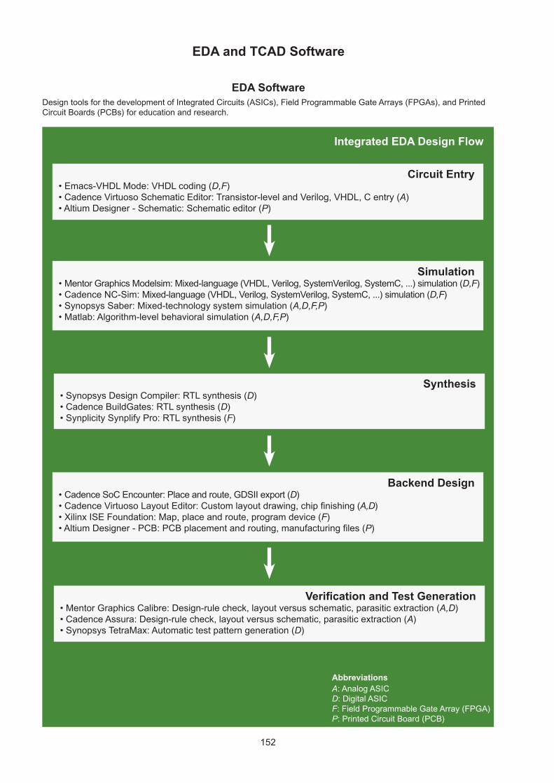
152
EDA SoftwareDesign tools for the development of Integrated Circuits (ASICs), Field Programmable Gate Arrays (FPGAs), and Printed Circuit Boards (PCBs) for education and research.
EDA and TCAD Software
AbbreviationsA: Analog ASICD: Digital ASICF: Field Programmable Gate Array (FPGA)P: Printed Circuit Board (PCB)
Integrated EDA Design Flow
Circuit Entry• Emacs-VHDL Mode: VHDL coding (D,F)• Cadence Virtuoso Schematic Editor: Transistor-level and Verilog, VHDL, C entry (A)• Altium Designer - Schematic: Schematic editor (P)
Simulation• Mentor Graphics Modelsim: Mixed-language (VHDL, Verilog, SystemVerilog, SystemC, ...) simulation (D,F)• Cadence NC-Sim: Mixed-language (VHDL, Verilog, SystemVerilog, SystemC, ...) simulation (D,F)• Synopsys Saber: Mixed-technology system simulation (A,D,F,P)• Matlab: Algorithm-level behavioral simulation (A,D,F,P)
Synthesis• Synopsys Design Compiler: RTL synthesis (D)• Cadence BuildGates: RTL synthesis (D)• Synplicity Synplify Pro: RTL synthesis (F)
Backend Design• Cadence SoC Encounter: Place and route, GDSII export (D)• Cadence Virtuoso Layout Editor: Custom layout drawing, chip finishing (A,D)• Xilinx ISE Foundation: Map, place and route, program device (F)• Altium Designer - PCB: PCB placement and routing, manufacturing files (P)
Verification and Test Generation• Mentor Graphics Calibre: Design-rule check, layout versus schematic, parasitic extraction (A,D)• Cadence Assura: Design-rule check, layout versus schematic, parasitic extraction (A)• Synopsys TetraMax: Automatic test pattern generation (D)
153
TCAD Software
Technology CAD (TCAD) for technology and device development in nanoelectronics and optoelectronics.
Commercial tools of Synopsys, Inc. used in research and education.
Integrated TCAD Flow
FrameworkSentaurus Workbench• workbench for technology and device development• simulation projects to automate large-scale simulation, parameterization of simulations• yield optimization and failure analysis• sensitivity analysis and design-of-experiments• advanced 2D and 3D visualization
LibraryCalibration Library• database of SIMS doping profiles• to calibrate process model parameters• analysis and optimization of process
technology
Structure EditorSentaurus Structure Editor• 2D and 3D device structure editor• meshing engines
Process SimulationSentaurus Process• 1D, 2D and 3D process simulator• optimizing silicon and compound semicon-
ductor process technologies
Device SimulationSentaurus Device• advanced multidimensional device simulator• electrical, thermal, and optical charac-
teristics of silicon-based and compound semiconductor devices
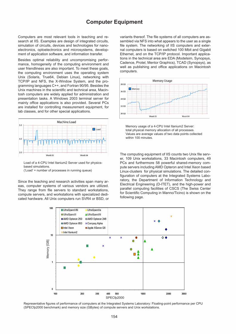
154
Computers are most relevant tools in teaching and re-search at IIS. Examples are design of integrated circuits, simulation of circuits, devices and technologies for nano-electronics, optoelectronics and microsystems, develop-ment of application software, and information transfer.
Besides optimal reliability and uncompromising perfor-mance, homogeneity of the computing environment and user friendliness are also important. To meet these goals, the computing environment uses the operating system Unix (Solaris, True64, Debian Linux), networking with TCP/IP and NFS, the X-Window System, and the pro-gramming languages C++, and Fortran 90/95. Besides the Unix machines in the scientific and technical area, Macin-tosh computers are widely applied for administration and presentation tasks. A Windows 2003 terminal server for mainly office applications is also provided. Several PCs are installed for controlling measurement equipment, for lab classes, and for other special applications.
Since the teaching and research activities span many ar-eas, computer systems of various vendors are utilized. They range from file servers to standard workstations, compute servers, and workstations with specialized dedi-cated hardware. All Unix computers run SVR4 or BSD, or
variants thereof. The file systems of all computers are as-sembled via NFS into what appears to the user as a single file system. The networking of IIS computers and exter-nal computers is based on switched 100 Mbit and Gigabit Ethernet, and on the TCP/IP protocol. Important applica-tions in the technical area are EDA (Modelsim, Synopsys, Cadence, Protel, Mentor Graphics), TCAD (Synopsys), as well as publishing and office applications on Macintosh computers.
The computing equipment of IIS counts two Unix file serv-er, 109 Unix workstations, 33 Macintosh computers, 49 PCs and furthermore 58 powerful shared-memory com-pute servers including AMD Opteron and Intel Xeon based Linux-clusters for physical simulations. The detailed con-figuration of computers at the Integrated Systems Labo-ratory, the Department of Information Technology and Electrical Engineering (D-ITET), and the high-power and parallel computing facilities of CSCS (The Swiss Center for Scientific Computing in Manno/Ticino) is shown on the following page.
Computer Equipment
Representative figures of performance of computers at the Integrated Systems Laboratory: Floating-point performance per CPU (SPECfp2000 benchmark) and memory size (GBytes) of compute servers and Unix workstations.
Load of a 4-CPU Intel Itanium2 Server used for physics-based simulations.(‘Load’ = number of processes in running queue)
Memory usage of a 4-CPU Intel Itanium2 Server:total physical memory allocation of all processes. Values are average values of two data points collected within 100 minutes.
SPECfp2000
Mem
ory
[GB
]
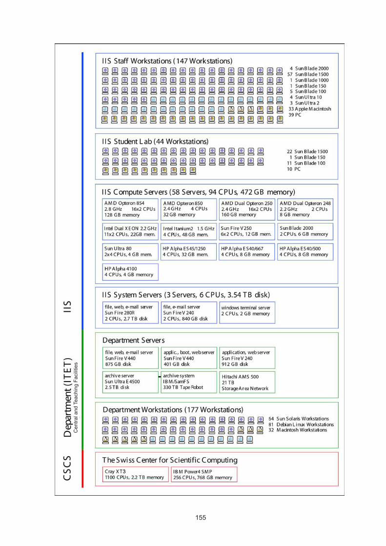
155
Cen
tral
and
Tea
chin
g F
acili
ties