research highlights 2010 - wpi-aimr.tohoku.ac.jp · as materials science, physics, chemistry and...
TRANSCRIPT

RESEARCH H
IGHLIGH
TS 2010
RESEARCH HIGHLIGHTS 2010A publication of the WPI Advanced Institute for Materials Research
Advanced Institute for Materials Research
Tohoku University
SCIENTIFIC COMMUNICATIONS
IN THE SPOTLIGHT
37AIMResearch 2010
What kind of research do you do at the WPI-AIMR?
Caron: I am a research associate working in the BMG Research Group. I use acoustic methods, such as ultrasound and near-field sound, to study the mechanical properties, particularly frictional properties, of BMGs. I did my PhD at Saarland University and a postdoc at the University of Ulm, both in Germany. Since I moved to the WPI-AIMR, I have been using SPM to study the mechanical properties of BMGs.
What was the application process like?
Caron: The first thing I did was to send a CV and a cover letter to the WPI-AIMR. Then I met Professor Dmitri Louzguine, my present boss, in Sendai and we dis-cussed what we could do together. He got quite interested. Three months after my application, I came to Japan.
Does the WPI-AIMR provide assistance for foreign researchers?
Caron: Yes. They provide support for administrative issues, such as fund-ing applications, and for our daily life. Whenever we have problems, we go to see Director Yoshinori Yamamoto or the institute’s secretariat.
Doctor Nakajima, could you tell me more about your current projects?
Nakajima: Polymers cannot be used as single-component materials. You need to mix a polymer with, say, another polymer or an inorganic material. In this case, the interface between the two materials be-comes important. Doctor Xu and I are now studying the interfacial properties of poly-mers. I am also working with researchers on BMGs. We are planning to mix materi-als to make new functional materials. I am not sure if it will work, but this is our goal.
Doctor Xu, could your model be applied to Dr Nakajima’s work?
Xu: That is the dream! My model works well in theory, but I do not know how good it works for real materials. The advantage of my model is that it is quite general. However, there are some specific questions that I still need to answer. One of the big-gest questions in materials science right now is how do we make stable BMGs — or in other words, BMGs that do not crystal-lize easily. My job is to provide the theoreti-cal basis for finding such stable BMGs. My model shows that it is possible to make stable BMGs through polymorphisms, or glass–glass transitions.
Doctors Ueno and Caron, could you tell me about your current projects? Who are you collaborating with at the WPI-AIMR?
Ueno: I am collaborating with Dr Akagi of Prof. Tsukada’s group, who performs theo-retical simulations of the interface between organic polymer and other materials. My device applications rely on the interface between ceramic and organic materials, so the collaborative study can provide invalu-able information.
Caron: I am collaborating with Dr Nakajima to study friction in BMGs. BMGs have the potential to be used in micro-devices, such as microelectromechanical systems (MEMS), so their properties on the microscale are very interesting. We study the frictional properties between silicon and BMGs and try to understand the role of the oxide layer, as well as the relaxation state of the BMG. Doctor Nakajima is bringing his experience in SPM to the experiment.
How are BMGs used in MEMS?
Caron: BMGs can be processed in an undercooled liquid state. You can heat
them up above the glass transition, and in the undercooled liquid state, they are really easy to form into devices such as microge-ars and cantilevers.
What are your goals in the short term? What are some of the challenges?
Nakajima: One of WPI-AIMR’s missions is to bridge conventional disciplines, such as materials science, physics, chemistry and engineering, to create new functional materials — the so-called ‘fusion research’. I think this is very important. We have people from the BMG group, semicon-ductor group, polymer group and soft materials group working together. This is a unique structure. The WPI-AIMR holds seminars regularly and we are starting to understand each other and the different disciplines. However, we are now beginning to realize the difficulty in doing fusion research. I think we will create something new in the future, but this is not something that happens overnight.
Xu: Yes, I know what you mean. It takes time. For me, I find that I have a very different background from most people here — they are more like engineers and I am more theoretical. There is a big gap. If I go to the seminar, I will get something, but it will not be on the same level as when I used to go to seminars in my field. The information I am receiving is huge. As a newcomer, it is difficult to get to the es-sential part immediately.
Ueno: The good thing about the WPI-AIMR is that the laboratory doors are always open. If I need to find someone to discuss something, I can reach them easily. In addition, my contacts at the WPI-AIMR are not limited to physics, but also include other fields such as biol-ogy and chemistry. This provides a good opportunity for me to broaden my scope and grow.
Caron: Even with institute members overseas, communication is still quite easy. There is Skype and email, and they visit several times a year. It is quite easy to discuss our research.
“The WPI-AIMR is a very international institute where I get to interact
with people from different fields and nationalities.”
ArnAud CAron
“The good thing about the WPI-AIMR is that the laboratory doors are always open.”KAzunori ueno
WPI Advanced Institute for Materials Research
The Advanced Institute for Materials Research (AIMR) at Tohoku University in Sendai, Japan, is one of six World Premier International (WPI) Research Centers established with the support of the Japanese Ministry of Education, Culture, Sport, Science and Technology (MEXT). Since its inauguration in 2007, the WPI-AIMR has been bringing together world-class researchers from Japan and abroad to carry out cutting-edge research in materials science through interdisciplinary collaboration among its four groups: Bulk Metallic Glasses, Materials Physics, Soft Materials, and Device/Systems.
Led by chief scientist and institute director Yoshinori Yamamoto, the center promotes fusion research across the different groups while fostering young researchers through a fusion-research proposal system and the Global Intellectual Incubation and Integration Laboratory (GI3 Lab), where international joint research is carried out in close cooperation with high-profile researchers invited from countries throughout the world.
The WPI-AIMR is host to over 100 leading researchers from around the world including 32 principal investigators. In addition to the research hub at Tohoku University, the WPI-AIMR collaborates with research centers in the UK, France, Germany, the USA and China. Close ties with other leading foreign universities are maintained through its international networks.
AIMResearch
AIMResearch is an online and print publication that highlights the scientific achievements and activities of the WPI-AIMR. First published in June 2009, AIMResearch selects the most important papers from the wealth of research produced by WPI-AIMR scientists throughout the year, distilling the essence of the achievements into timely, concise and accessible research highlights that are easy to digest but retain all of the impact and importance of the original research article. Published monthly on the AIMResearch website in both English and Japanese, AIMResearch highlights bring the very best of WPI-AIMR research to a global audience of specialists and nonspecialists alike. AIMResearch also publishes a range of features articles introducing other activities of the WPI-AIMR’s research groups. Visitors to the website can register for monthly email alerts in either Japanese or English to keep abreast of the latest developments and discoveries made at the WPI-AIMR.
research.wpi-aimr.tohoku.ac.jp
RESEARCH HIGHLIGHTS 2010
© 2011 Tohoku University

MESSAGE FROM THE DIRECTORGreen materials
RESEARCH HIGHLIGHTSNanotechnology: metallic glass nanowires Oxide electronics: A robust gate Organic gels: Dynamic duos Interfaces: An in-depth picture Spin dynamics: A nano-spinning top Printable electronics: A little give and takeIron-based superconductors: Borrowing from graphene Nanomaterials: Supersizing at the nanoscale Metallic glass: Go with the flowPolymers: Atomic mapping Photonics: Bright white light Atomic-scale imaging: Stepping up the paceClathrates: Rattling the cageSingle-molecule imaging: Finished in chromeOxides: Approaching perfectionIron-based superconductors: Spin mattersTopological insulators: A large leap aheadSuperconductors: A sound solutionNanostructured catalysts: Golden openingsMetals: Bringing glass to orderOxides: Less is more
2
6789
1011121314151617181920212223242526
In THE SPOTLIGHTTime to shake things up MEMS technology makes the world a merrier placeFusion research on the global stageMixing the unmixableFrom the bottom upLearning the difference
2829
31323436
research.wpi-aimr.tohoku.ac.jp
AIMResearch is a publication of the World Premier International Advanced Institute for Materials Research (WPI-AIMR), a Tohoku University institute funded by the Ministry of Education, Culture, Sports, Science and Technology of Japan.
© 2011 WPI-AIMR, Tohoku University. This publication may be reproduced in its original form for personal use only. Modification or commercial use without prior permission from the copyright holder is prohibited.
EditorialWPI-AIMR, Tohoku University2-1-1 Katahira, Aoba-ku, Sendai,Miyagi 980-8577, Japan
Editor-in-Chief Yoshinori YamamotoManaging Editor Masashi KawasakiEditorial Assistant Mariko Onodera
ISSN 1884-491X
© 2011 Tohoku University

As the institute director of the World Premier International Advanced Institute for Materials Research (WPI-AIMR), I have great pleasure in welcoming you to this, the second print edition of AIMResearch. In April, the AIMResearch website entered its second year, and this print publica-tion is a comprehensive collection of the research highlights published on the website in 2010 along with lively journalistic features that turn a spotlight on the people and activities behind the research carried out at the WPI-AIMR.
The importance of materials science to scientists and society in general continues to grow on an annual basis — a point clearly underlined by the awarding of the 2010 Nobel Prize in Physics for the discovery of graphene, one of the most exciting discoveries in materials science in recent years.
When the WPI-AIMR was inaugurated in 2007, its scientific objectives were threefold. Firstly, to create new substances and materials with innovative
functions by new methods of atom and molecular control; secondly, to construct devices based upon new fundamental research; and finally, to contribute to society by promoting applied research projects on materials and system architectures capable of delivering concrete benefits to humankind.
In October 2010, the WPI-AIMR celebrated its third anniversary and the attainment of this milestone provided an ideal opportunity to consolidate the long-term strategy of the institute and to define more clearly its research direction and vision. Based on the experience and research outcomes garnered over the past three years, it has become clear that the future of the WPI-AIMR lies in the development of green materials.
While there are many areas in which green materials can play an important role, we have identified fields such as energy harvesting, energy saving and environmental clean-up as high priorities. In the arena of energy harvesting,
the WPI-AIMR will target the creation of new materials for photovoltaic and thermoelectric conversion, while research on energy-conserving technologies will concentrate on cutting-edge materials for soft electronics, superconductors, low friction, low wear, lubricants and low energy consumption logic and memory circuits based on magnetic materials. Environmental clean-up is another topic of growing im-portance and the WPI-AIMR will turn its focus on green innovation to the discovery of new catalysts, porous materials, sensors, micro-electromechanical systems and biodevices for applications in this area. The basis of these component technologies lies in the research and development of green materi-als with functional properties that fulfill key objectives.
The theme of green innovation is a diverse and complex one that requires comprehensive and imaginative use of component technologies. It is not possible to confront the demands placed on
MESSAGE FROM THE DIRECTOR
Green materials
© 2011 Tohoku University

green materials and innovative component technologies through the use of a single material. Rather, it is necessary to investigate and explore heteromaterials formed by the combination of two or more different materials and to use their individual characteristics synergis-tically to bring out new innovative functional properties.
For example, ‘hard’ metallic glasses and ‘soft’ polymers constitute, in a static sense, very different systems. However, looked at dynamically, both systems are non-equilibrium materials and this common property makes it easy to fabricate composite materials from a combination of metallic glasses and polymers, which may find applications, for example, as a low-wear rubber. Palladium catalysis for cross-coupling, the discovery for which was awarded the Nobel Prize in Chemistry in 2010, is another example. Although an incredibly powerful and versatile technique, the products of these reactions are often contaminated
with traces of the palladium metal used in the catalysis, which limits the approach’s usefulness in reactions demanding extremely high levels of product purity, such as those involved in the synthesis of pharmaceutical drugs. Our research has shown that nanopo-rous palladium-based catalysts containing a combination of palladium and nickel may offer a solution via heterophase-interface control, which is essential for the realization of the full power of heteromaterial synergetics.
These are just two examples of the ways in which the WPI-AIMR is involved in developing new tools and techniques for basic research into green materials. By pursuing and deepening this kind of basic research, I believe that the WPI-AIMR will become established as a visible and globally recognized research center for green materials in the coming years.
Yoshinori YamamotoDirectorWPI-AIMR
© 2011 Tohoku University

research.wpi-aimr.tohoku.ac.jp
All articles published on AIMResearch can be accessed free of charge. Register for monthly email alerts to get the latest research news from
WPI-AIMR delivered direct to your inbox!
AIMResearch introduces the best of research from the WPI-AIMR in the form of concise, accessible research highlights and casts a spotlight on the
scientists and laboratories behind one of the world's leading institutes for the development of new and innovative functional materials.
AIMResearch is an online publication that highlights the best of cutting-edge research carried out at the World Premier International Advanced Institute for Materials Research (WPI-AIMR),
a leading interdisciplinary and internationally focused center of materials science research based at Tohoku University in Japan.
© 2011 Tohoku University

RESEARCH HIGHLIGHTSThe WPI-AIMR advances research in bulk metallic glasses, materials physics, soft materials and device/systems construc-tion, and actively promotes collaboration among these divisions toward the development of ground-breaking technologies that cross the boundaries of conventional fields of study — bridging the disciplines of materials science, physics, chemistry and precision, mechanical, electronics and information engineering.
© 2011 Tohoku University

RESEARCH HIGHLIGHTS
6 AIMResearch 2010
Metallic glass (MG) is a promising class of material that could find potential use in structural components for ap-plications ranging from mobile phone casings to biomedical implants. At the same time, achieving MG structures on the nanoscale, which could lead to novel applications, has remained a challenge. Researchers from Tohoku University’s WPI-AIMR have now developed a controlled method for producing MG nanowires with very high mechanical elasticity and strength1.
Metallic glasses are amorphous — like window glass except that they are made from metal alloys. Even though their appearance is similar to that of crystal-line metallic alloys, such as steel, their amorphous structure leads to a number of advantageous properties. For example, in steels and other crystalline metals, imperfections such as vacancies, disloca-tions and grain boundaries in the crystal structure are the main cause of mechani-cal failure. Owing to their amorphous structure, however, “MGs possess a com-bination of unique properties including ultrahigh strength, high hardness and high resistance to wear corrosion,” ac-cording to Koji Nakayama, who leads the WPI-AIMR fusion research team.
Remarkable progress has been achieved in exploring alloy compositions that are best suited for the fabrication of MGs in bulk quantities — a requirement for practical utilization of these unusual materials. However, while achievements in this area have been significant, far less attention has been paid to MG nano-structures, such as ultrathin wires.
Metallic glass nanowires were first reported in 2008 by the same group while studying the compression of
bulk MGs. The surfaces of bulk MGs typically get very hot during the fracture process, which leads to the formation of nanowires. Now, the researchers have developed a mechanism to draw MG ribbons in a much more controlled fashion. Their method is based on super-plastic deformation, following a simple principle that glass blowers have been using for centuries. The MG is processed when it is still in a viscous liquid state and, with the help of a weight attached to the ribbon, is drawn out into nanowires by a custom-made machine.
The nanowires obtained by this method display excellent mechanical properties — they can be bent elasti-cally (see image) while overall retaining strength comparable to that of the bulk
material. Furthermore, the versatil-ity of the drawing process ensures that nanowires can be formed from MGs with a broad range of compositions. “In terms of applications, palladium-based MG nanowires could be used as sensors with high hydrogen sensitivity. Iron-based MG, on the other hand, exhibits soft magnetic properties that could be useful in ultrahigh magnetic-field sen-sors for biomagnetic measurements,” says Nakayama.
1. Nakayama, K.S., Yokoyama, Y., Ono, T., Chen,
M.W., Akiyama, K., Sakurai, T. & Inoue, A.
Controlled formation and mechanical character-
ization of metallic glassy nanowires. Advanced
Materials 22, 872–875 (2010).
A flexible metallic glass nanowire. The ribbon sample from which the nanowire is drawn is visible on the left.
The free end of the wire in the center oscillates with a sine-wave-like pattern.
500 μm
Nanotechnology
Metallic glass nanowiresNanowires made from metallic glass are extremely tough and hold promise for a large number of nanotechnology applications
© 2011 Tohoku University

RESEARCH HIGHLIGHTS
7AIMResearch 2010
Silicon and other covalent bond-ing semiconductors have been the primary materials used in electronic components for several decades, but the need to improve performance and develop novel functionalities has spurred research efforts into new ma-terials. Particularly promising are the highly conductive ‘two-dimensional electron gases’ that form at the inter-faces between insulating oxides — for example between LaAlO3/SrTiO3 and MgxZn1–xO/ZnO — in which electrons move freely in two dimensions.
Incorporating such interfaces into electronic devices such as transistors requires the ability to tune the carrier concentration by applying a voltage be-tween a gate electrode and the interface itself. This is what Masashi Kawasaki and colleagues at the WPI-AIMR have now successfully demonstrated by con-structing a transistor using a polymer gate and a MgxZn1–xO/ZnO interface as the active layer1.
When a metallic gate is deposited on a semiconductor, the difference in work function — the energy required for an electron to leave the surface — between the two parts leads to the formation of a Schottky junction, which allows the carrier concentration in the semicon-ductor to be altered with minimal leak-age current from the gate. As Kawasaki explains, however, “Schottky junctions involving ZnO and noble metals have not been adequately reproducible and the device characteristics are far from excellent. We suspect that the metals react with oxygen in the ZnO somehow, which induces defects.” The issue is even more delicate in the case of inter-faces, as any small defect creates a path
for the current to leak from the gate, which has a very damaging effect on the properties of the two-dimensional electron gas.
“Polymers are usually very stable against oxidation, and atoms in poly-mers are already saturated with chemical bonds,” says Kawasaki. The team fabri-cated a transistors using a high-mobility MgxZn1–xO/ZnO interface and a layer of a conducting polymer for the gate (see figure). The polymer, PEDOT:PSS, is commercially available and widely used in organic displays.
The two-dimensional electron gas exhibits sharp resistance oscillations under a magnetic field due to the quantum Hall effect, which confirms the excellent quality of the device. In addition, the oscillations are clearly modulated by the application of a gate voltage, demonstrating that the carrier
concentration can be tuned externally.The results could be very significant
for practical applications. “This in-terface could be one of the important ingredients for future transparent circuitry. The fabrication method is extremely simple and the materials are of low cost,” says Kawasaki. There is also no reason why the same route could not be followed for other conducting oxides: the team has already explored the possibility of using the same poly-mer as a gate for oxides such as SrTiO3 or TiO2.
1. Nakano, M., Tsukazaki, A., Ohtomo, A., Ueno, K.,
Akasaka, S., Yuji, H., Nakahara, K., Fukumura, T. &
Kawasaki, M. Electric-field control of two-
dimensional electrons in polymer-gated–oxide
semiconductor heterostructures. Advanced
Materials 22, 876–879 (2009).
Top view (left) of the transistor and schematic illustration (right) showing the two-dimensional electron gas
interface between ZnO and MgZnO.
Oxide electronics
A robust gateHigh-quality transistors can be fabricated using an oxide interface and a polymer gate
e
PEDOT:PSS
ee ee e e ee eee eeee eee2D electro
ns
ZnO
MgZnO
100 μm
© 2011 Tohoku University

RESEARCH HIGHLIGHTS
8 AIMResearch 2010
Ever since the realization that biomol-ecules such as DNA naturally assemble into three-dimensional helix shapes, researchers have tried to replicate these structures using different chemical units. Helicenes — spiral-shaped mol-ecules made up of several fused benzene rings — have attracted much scientific interest because their conjugated frame-work leads to unique optical, electronic and aggregation properties.
Now, Masahiko Yamaguchi from the WPI-AIMR at Tohoku University1 and colleagues have used short chains of he-licenes, known as oligomers, to produce thermally reversible organic gels. The methodology developed by the research team promises to improve control over the properties of these hybrid liquid–solid materials at the molecular level.
When helicenes are synthesized, they form one of two chiral enantiomers — isomers of the same compound but ar-ranged such that they are mirror images of one another. Most reactions produce equal amounts of both enantiomers, but these racemic mixtures usually form crystals with well-ordered lattices, not gels. In pure solutions of enantiomers, however, the tight packing needed for crystallization is perturbed, and the he-licenes tend to aggregate into long fibers that trap solvent molecules in a gel.
Yamaguchi and his team developed a new series of ‘pseudoenantiomers’, which display better gel-forming prop-erties than pure solutions. Composed of two helicene enantiomers with slightly different sizes, these substances sponta-neously formed a yellow gel (pictured) when mixed together at room tem-perature. Furthermore, this process was thermally reversible: heating to 110 °C
caused the gel to liquefy, but the gel re-formed on cooling to 25 °C. Yamaguchi says that the pseudoenantiomers take on properties that are intermediate between those of the pure enantiomers and the racemic mixture, suppressing crystal-lization and enhancing fiber formation.
The need for soft gel-based materials is expanding in diverse areas ranging from bioengineering to consumer packaging. Gels are suitable for these applications because of their ability to mimic the networks found in living systems and present properties distinct from those of conventional materials. Yamaguchi’s pseudoenantiomer method has the potential to improve gel com-pounds by providing a reliable means of joining small molecules together.
“Precisely constructing gels with specific functions, such as hardness, elasticity, flexibility or processability, requires a delicate method to control the
gel structure,” says Yamaguchi. “In that sense, gel formation by small molecule aggregation is interesting because the structure of small molecules can be readily controlled, and a diversity of gels can be provided.”
The use of two-component gels offers great promise in terms of tuning prop-erties, as different enantiomers ratios produce different gels. It also has other implications, according to Yamaguchi: “For example, one compound can be on a surface, and the other in solution. Such a system can provide control of the interface structure between the solid and liquid.”
1. Amemiya, R., Mizutani, M. & Yamaguchi, M. Two-
component gel formation by pseudoenantio-
meric ethynylhelicene oligomers. Angewandte
Chemie International Edition
49, 1995–1999 (2010).
A new thermally reversible gel (inset) forms long fibrous aggregates (atomic force microscopy image) thanks
to a two-part mixture of pseudoenantiomers.
0.5 μm
Organic gels
Dynamic duosA two-part mixture of molecular helices proves to be a versatile route towards functional soft materials
© 2011 Tohoku University

RESEARCH HIGHLIGHTS
9AIMResearch 2010
The arrangement of atoms at the inter-face between a metal and a semiconduc-tor plays a crucial role in determining the efficiency of electronic devices. But imaging atoms buried deep beneath the surface is not an easy task. Yuichi Ikuhara and co-workers from Tohoku University and Tokyo University1 have now produced an atomic-level picture of these technologically im-portant interfaces by combining state-of-the-art imaging techniques and numerical simulations.
“Because we need to connect electrical components together using wires, a key issue that currently limits the efficiency of electronic circuits is the manufacture of reliable, low-resistance contacts between a metal and a semiconductor,” explains Zhongchang Wang, a member of the WPI-AIMR. A high-resistance barrier formed at some metal–semicon-ductor interfaces, known as a Schottky barrier, hinders the flow of electrons and increases power dissipation.
A good choice of metal and a process known as annealing — quickly heating to a high temperature — can overcome Schottky barriers. In the case of silicon carbide (SiC), a wide-bandgap semi-conductor with potential applications in high-power and high-temperature appli-cations, a trial-and-error approach has determined that titanium–aluminum (TiAl) alloys form such low-resistance contacts with SiC. “Researchers have suggested that a new metallic compound, Ti3SiC2, is formed between the deposited TiAl alloy and the SiC; however, it re-mained unclear how this interface could reduce the contact resistance.”
Ikuhara and his team deposited alter-nating layers of titanium and aluminum
on a SiC substrate and then annealed them at 1,000 °C for a few minutes. They then produced an image (pictured) of the precise arrangement of the atoms at the interface using a powerful technique known as Z-contrast scanning trans-mission electron microscopy (STEM), which is capable of distinguishing differ-ent atomic species. The titanium atoms appeared as bright spots whereas the silicon atoms were much darker.
Numerical calculations simulated 96 possible interface geometries; only two of which matched the STEM image. In both of these variations, the silicon atoms in the metal (Ti3SiC2) sat in the spaces between silicon atoms in the semiconductor (SiC). In one case, however, carbon atoms, not visible in
the STEM image because of their low mass, were also present at the interface (SiCSi). Further calculations indicated that this SiCSi arrangement was more stable than the other candidate (an SiSi interface) and that the presence of the carbon led to a much smaller Schottky barrier. “Our results suggest that an atomic layer of carbon plays an important role in reducing the contact resistance and provides a strategy for producing efficient SiC contacts,” says Wang.
1. Wang, Z., Saito, M., Tsukimoto, S. & Ikuhara, Y.
Interface atomic-scale structure and its impact
on quantum electron transport. Advanced
Materials 21, 4966–4969 (2009).
Z-contrast STEM image of the position of atoms at the interface between SiC and Ti3SiC
2. Titanium atoms are
circled in yellow, and silicon atoms in green. Carbon atoms, shown as white dots, are not evident in the image
but their position is inferred from a theoretical model.
3 Å
SiC
Ti3SiC2
Interfaces
An in-depth pictureCarbon atoms are important for creating efficient metallic contacts with wide-bandgap silicon carbide
© 2
010
Z. W
ang
© 2011 Tohoku University

RESEARCH HIGHLIGHTS
10 AIMResearch 2010
The need for ever-increasing information storage capacity is motivating research-ers to investigate various systems for reducing the size of the basic storage ele-ments and increasing the speed at which data can be written and read. A structure that has recently received considerable attention is ‘spin transfer torque’ (STT) magnetic random access memory (MRAM), which is based on arrays of magnetic tunneling junctions. In such a device, the information is stored in the magnetization of a ferromagnetic film, and is controlled by an electrical current applied through the STT interaction. Shigemi Mizukami and colleagues from the WPI-AIMR and Tohoku University1 have now observed the fast motion of spins in a cobalt film just a few atomic layers thick (0.5–4.0 nm) sandwiched between layers of platinum. “Spin moves constantly, like a bar magnet, in a memory cell, and it experiences ‘friction’, even though it’s a quantum mechani-cal object. This friction, called ‘Gilbert damping’, influences power consumption and speed in devices,” says Mizukami. The researchers’ experiments allowed the friction strength acting on the motion of spin in the cobalt film to be determined precisely for the first time (see figure).
In an ideal STT-MRAM element, the minimum current density needed to switch the magnetization should be the lowest physically possible — a value that is proportional to the Gilbert damp-ing constant α, and the perpendicular magnetic anisotropy Heff. However, changes in Heff also affect thermal stabil-ity. It is therefore crucial to understand how α and Heff are related in order to design the struc tures that provide optimal performance.
Previous theoretical investigations have suggested that there is a linear rela-tionship between α and Heff, but this has yet to be confirmed because it is difficult to observe spin dynamics at high frequen-cies and in ultrathin films. Mizukami’s team developed a special instrument for performing ultrafast time-resolved magneto-optical Kerr effect experiments, which allowed the researchers to derive values for both α and Heff.
The results showed that Heff is inverse-ly proportional to the thickness of the cobalt layer, whereas α increases linearly up to a cobalt layer thickness of 1 nm be-fore increasing more rapidly. Mizukami considers that this behavior could reflect the transition from perpendicular to
parallel magnetization in the cobalt film. “Our experiments demonstrated that Gilbert damping in the cobalt/platinum system can be tuned widely. It is crucial for spintronics applications to optimize Gilbert damping, while maintaining high Heff, in order to achieve high speed and low power consumption,” says Mizukami. The results therefore represent an important step towards the design of applications based on STT.
1. Mizukami, S., Sajitha, E.P., Watanabe, D., Wu, F.,
Miyazaki, T., Naganuma, H., Oogane, M. & Ando,
Y. Gilbert damping in perpendicularly magne-
tized Pt/Co/Pt films investigated by all-optical
pump-probe technique. Applied Physics Letters
96, 152502 (2010).
(Upper) Schematic diagram of an MRAM element and spin dynamics for writing from “0” to “1”. Spin is illustrated
by permanent ‘bar’ magnets (red and blue). (Lower) Spin motion observed in a 0.9 nm-thick cobalt layer.
0 100 200
Kerr
sign
al
(arb
. uni
t)
Pump-probe delay time (ps)
0.9 nm-thick cobalt
0
1
NSN
S
Spin dynamics
A nano-spinning topTime-resolved experiments reveal details of spin motion in magnetic nanostructures, contributing to the development of high-speed spintronic devices with lower power consumption
© 2011 Tohoku University

RESEARCH HIGHLIGHTS
11AIMResearch 2010
Innovative technologies that use molecular-based ‘inks’ to print electronic circuitry onto flexible plastic substrates promise to usher in an era of futuristic low-cost devices, such as smart clothing tags that can communicate instructions to washing machines. Manufacturing printable electronics remains challeng-ing, however, because the high tempera-tures usually needed to bind the inks to surfaces can damage the polymer materi-als used as substrates.
Researchers led by Daisuke Hojo and Tadafumi Adschiri from the WPI-AIMR at Tohoku University have now developed a simple and efficient way to attach an ink made of metal oxide nanocrystals onto surfaces at room temperature1. According to Hojo and Adschiri, the diverse condi-tions needed to deposit extremely small particles in an organized manner made this breakthrough a tough one to achieve. “For printable electronics, the nanopar-ticles have to be well-dispersed in sol-vents, but they also need to self-assemble into films during the drying stage, and to subsequently become immobilized on the substrate,” says Hojo. “For each step, the required interactions between the nanoparticles, the solvent, and the surface are different — making the fabrication process difficult,” says Adschiri.
Researchers at Tohoku University led by Adschiri had previously been successful in coating tiny particles of cerium oxide — a rare-earth compound with catalytic and optical capabilities — with a thin film of organic molecules to prepare highly soluble nanocrystals2. Using a process known as ligand exchange, the researchers demonstrated in their most recent study that cerium oxide nanocrystals can be im-mobilized on a silica surface by replacing
one molecule bound to the nanocrystal with one bound to the substrate — achiev-ing the effect of a chemical ‘glue’.
The scientists prepared the metal oxide nanocrystals for the process by coating the particles with decanoic acid, a long carboxylic acid that binds to cerium oxide via two oxygen atoms. They then deposited the nanocrystals from solu-tion at room temperature onto a silicon surface that had been coated with a thin organic layer of DHCA — a hydrocarbon bearing a catechol group (a benzene ring with two neighboring alcohol units). Chemical equilibrium effects drove the nanocrystals to swap the decanoic acid for the more favorable catechol groups fixed on the silica surface (see figure), effectively binding the nanocrystals to the substrate.
The researchers confirmed that this method produced dense films of surface-bound nanocrystals that were thermally stable up to 200 °C. They also found that
other carboxylic acid-coated nanocrys-tals, including crystals with iron and titanium cores, could be trapped using the same technique because of the broad affinity of catechol groups. According to Hojo and Adschiri, this ligand-exchange method helps solve the critical problem of immobilizing nanoparticles. “This is a definite step toward establishing tech-nology for printed electronics, especially for fabricating photovoltaic devices,” says Adschiri.
1. Hojo, D., Togashi, T., Iwasa, D., Arita, T., Minami,
K., Takami, S. & Adschiri, T. Fabrication of
two-dimensional structures of metal oxide
nanocrystals using Si substrate modified with
3,4-dihydroxyhydrocinnamic acid. Chemistry of
Materials 22, 1862–1869 (2010).
2. Zhang, J., Ohara, S., Umetsu, M., Naka, T.,
Hatakeyama, Y. & Adschiri, T. Colloidal ceria
nanocrystals: A tailor-made crystal morphology
in supercritical water. Advanced Materials
19, 203–206 (2007).
Nanocrystals bearing decanoic acid (left) can be fixed to a substrate bearing catechol groups by ligand exchange
— swapping one molecule for another. This room-temperature ink ‘printing’ technique produces dense films of
metallic nanoparticles (right, scanning electron microscopy image of nanocrystal film).
O
O O
O
O O
O
HN
Organic layer
Substrate
SiO
Nano-crystal
Printable electronics
A little give and takeA selective ‘ligand exchange’ reaction makes molecular-based inks easier to attach to surfaces
© 2
010
D. H
ojo
© 2011 Tohoku University

RESEARCH HIGHLIGHTS
12 AIMResearch 2010
The discovery of iron-based supercon-ductors in 2008 reenergized the field of superconductivity research, all the more so because the electronic properties of these new compounds have proved to be complex and full of surprises. Few, however, would have expected that these superconductors would display features similar to those of another material that has recently attracted the excitement of scientists — graphene.
A team of researchers led by Takashi Takahashi of the WPI-AIMR had been studying the iron-based compound BaFe2As2 in order to gain new insights into its magnetic properties, particu-larly with respect to the ‘spin-density wave’ (SDW) order previously reported for this material. The team discovered that the compound has a Dirac cone-like electronic band structure1 — the same feature that gives graphene its exceptional properties.
BaFe2As2 is the parent compound of one member of the iron-based superconductor family. It is widely accepted that superconductivity in these iron-based compounds, as in the cuprate superconductors, is present in the parent compound but suppressed by another property, usually magnetism. The parent compound is induced into its superconducting state by adding im-purity atoms and cooling it to extremely low temperature.
The researchers examined the parent compound BaFe2As2 using a technique known as angle-resolved photoemission spectroscopy, which revealed two bright points of photon emission in momen-tum space below the SDW temperature (see figure). Focusing on these points and studying emission as a function of
energy and momentum, the team then discovered the Dirac cone — a band structure that describes how electrons behave like massless relativistic particles at certain points in momentum space.
The similarity with graphene is not complete, however. While the Dirac cone of graphene is symmetric with respect to momentum, that for BaFe2As2
is distinctly asymmetric and displays small pocket-like features and nodes, features that present intriguing targets for future research.
The team’s results have broad implica-tions for many of the actively studied topics in solid-state physics. Aside from graphene, Dirac cones have also been observed in ‘topological insulators’, a class of materials that are at once both insulating in the bulk and metallic at the
edges. “Whoever would have thought that iron-based superconductors, one of the hottest materials in materials science, would exhibit low-energy phys-ics similar to graphene?” says Pierre Richard, one of the lead researchers involved in the discovery. “With our findings, people will have to think more carefully on the connection between all of these materials, which could lead to the development of new functional materials with exotic properties.”
1. Richard, P., Nakayama, K., Sato, T., Neupane, M.,
Xu, Y.-M., Bowen, J.H., Chen, G.F., Luo, J.L., Wang,
N.L., Dai, X., Fang, Z., Ding., H. & Takahashi. T.
Observation of Dirac cone electronic dispersion
in BaFe2As2. Physical Review Letters
104, 137001 (2010).
Schematic illustration of the Dirac cones in BaFe2As
2 and the bright points (Λ) in momentum–energy (k–E)
space. The atomic structure of the compound is shown on the right.
ΛM
E
ky
kx
BaFeAs
Iron-based superconductors
Borrowing from grapheneResearchers discover remarkable similarities between an iron-based superconductor compound and graphene carbon
© 2011 Tohoku University

RESEARCH HIGHLIGHTS
13AIMResearch 2010
In a range of advanced technologies that deal with mechanisms on the molecular scale, such as molecular electronics and drug delivery, bridging the gap between nanoscale objects and larger devices is of key importance. Constructing suit-able structures that can fulfill the roles of both nanoscale and bulk objects, however, has generally been performed by miniaturizing larger structures. A research team led by Masatsugu Shimomura and Takeshi Higuchi from the WPI-AIMR1 has now had success with the opposite approach — building structures from the nanoscale up by self-assembly.
Shimomura and Higuchi used an approach known as self-organized pre-cipitation (SORP) to produce nanoscale aggregates from block copolymers —structures containing multiple distinct polymer subunits. Polymer aggregates or particles are typically prepared by emulsion polymerization, which in-volves the use of surfactant-stabilized oil in water. “But with that method, it is difficult to synthesize nanostructured particles,” says Shimomura. “The SORP method, on the other hand, can produce block copolymer particles quite easily,” says Higuchi.
The SORP technique exploits differ-ences in polymer solubility between good and poor solvents. The research-ers created polymer nanoparticles of polystyrene and polyisoprene by adding water to a solution of these two micro-phases in an organic solvent. Two days later, after the solvent had evaporated, the team reacted the nanoparticles with an oxidant, causing the polyisoprene to become insoluble while leaving the polystyrene portion of the particles
intact. The two microphases could then be dissociated by adding the nanopar-ticles once more to an organic solvent.
Using block copolymers containing polystyrene and polyisoprene subunits of similar length, the researchers ob-tained suprapolymer structures consist-ing of evenly stacked and alternating polymer sheets. Imaging experiments revealed that the block copolymers first self-assembled into layered particles, which then dissociated into nanometer-sized disks of polyisoprene sandwiched between polystyrene layers (pictured). In contrast, block copolymers with sub-units of dissimilar length gave cylindri-cal polyisoprene nanoparticles coated with polystyrene chains.
Blends of the two individual polymers produced particles with two distinct
hemispheres, known as ‘Janus’ particles, which dissociated on oxidation into the two constituent halves. “The Janus particles can be applied as pigments for electronic paper,” says Shimomura. Mixtures of the polymer blend and the block copolymers, on the other hand, gave porous nanostructures, “which are applicable as carriers in drug delivery systems,” says Higuchi. The team is currently working on assembling the nanometer-sized disks and cylinders into higher-order structures.
1. Higuchi, T., Tajima, A., Motoyoshi, K., Yabu, H.
& Shimomura, M. Suprapolymer structures
from nanostructured polymer particles.
Angewandte Chemie International Edition
48, 5125–5128 (2009).
Scanning transmission electron microscopy images of nanoparticles consisting of stacked layers (left) that are
transformed into nanodisks (right) by oxidation and dissociation. Schematic illustrations show the polystyrene
(blue) and polyisoprene (green) components of the structures.
300 nm 500 nm
Nanomaterials
Supersizing at the nanoscalePolymer-based structures that bridge the nano- and microscopic scales can now be built from the nanoscale up
© 2011 Tohoku University

RESEARCH HIGHLIGHTS
14 AIMResearch 2010
Portable electronic devices of the future may use a secret ingredient to guard against dents and collisions — a tough new type of alloy called metallic glass. These materials, formed by rapidly cool-ing molten mixtures of metals, have a non-crystalline, tightly packed internal structure that makes them springier, stronger and more scratch-resistant than conventional crystalline metals. However, the random atomic distribu-tion inside metallic glasses also makes it difficult to optimize their mechanical properties, leading to problems such as shattering and sudden failure.
Mingwei Chen, Pengfei Guan and Takeshi Egami from the WPI-AIMR at Tohoku University have now performed computer simulations that provide new microscopic insights into how mechanical failure occurs in metallic glasses1. The team found that external stress — the act of pulling the mate-rial apart — induces a liquid-like ‘flow’ of atoms similar to that caused by an increase in temperature. Their findings uncover the mechanism by which these glassy states can form, with the promise of greatly improving the reliability of manufacture for these alloys.
Despite their rigidity, metallic glasses actually exist in a ‘jammed’ phase of mat-ter that falls between solids and liquids. Forcing hot mobile metal atoms into a mold and then cooling rapidly trans-forms the liquid into a ‘frozen’ glassy state. It is know that expanding the vol-ume or heating can make the atoms flow once more. Until now, however, the role of external stress on this jammed phase had remained controversial.
Chen and his co-workers performed their modeling using a computational
technique known as molecular dynam-ics simulation. They simulated the atomic movements in a zirconium–cop-per–aluminum metallic glass when subjected to a shear force that gradually stretched the glass apart under constant volume and temperature conditions (see figure). After numerous simula-tions considering a range of shear rates, the researchers observed that the metal atoms entered a state of steady viscous flow, similar to that of a liquid, before snapping apart.
Remarkably, the viscosity of the metal under stress was found to be similar to that associated with elevated temperature, and the researchers were
able to model the stress–temperature conditions needed to form either the jammed glassy state or flowing state. The similarity of the effects of tempera-ture and stress indicates that both effects influence atomic flow in a like manner. “This must reflect the simplicity of the dynamics of glasses at a deep level, hidden behind the apparent complexity of the phenomena and the structure,” says Chen.
1. Guan, P., Chen, M. & Egami, T. Stress-
temperature scaling for steady-state flow in
metallic glasses. Physical Review Letters
104, 205701 (2010).
Schematic illustration of the simulated metallic glass system under shear stress.
Al
Cu
Zr
Metallic glass
Go with the flowSimulating the movements of thousands of atoms reveals that stress can transform glassy states into flowing liquids
© 2011 Tohoku University
RESEARCH HIGHLIGHTS
15AIMResearch 2010
The physical properties of polymers are heavily dependent on their molecular structure, and much research effort is expended in obtaining a certain de-sired property, such as high strength or elasticity. Molecular structures are often tailored by preparing copoly-mers combining two or more different monomer building blocks. In one kind of copolymer called a ‘block’ copolymer, the different monomers form separate, homogeneous blocks rather than com-bining in a random arrangement. This block formation usually results in phase separation — the tendency for mono-mers to cluster with other monomers of the same type. Gaining insight into the specific physical properties of block copolymers therefore usually requires an understanding of the composition and properties of the separate blocks.
Dong Wang and co-workers from the WPI-AIMR at Tohoku University1
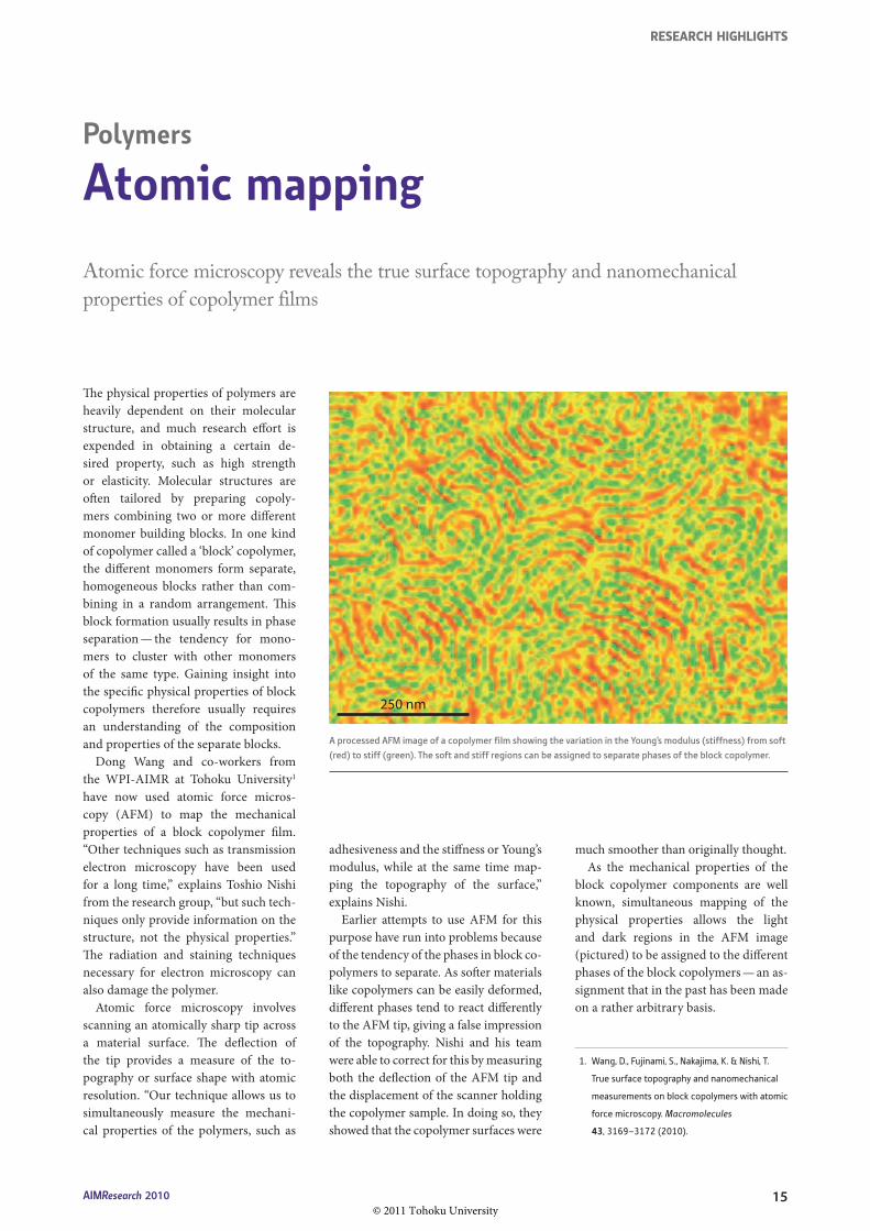
have now used atomic force micros-copy (AFM) to map the mechanical properties of a block copolymer film. “Other techniques such as transmission electron microscopy have been used for a long time,” explains Toshio Nishi from the research group, “but such tech-niques only provide information on the structure, not the physical properties.” The radiation and staining techniques necessary for electron microscopy can also damage the polymer.
Atomic force microscopy involves scanning an atomically sharp tip across a material surface. The deflection of the tip provides a measure of the to-pography or surface shape with atomic resolution. “Our technique allows us to simultaneously measure the mechani-cal properties of the polymers, such as
adhesiveness and the stiffness or Young’s modulus, while at the same time map-ping the topography of the surface,” explains Nishi.
Earlier attempts to use AFM for this purpose have run into problems because of the tendency of the phases in block co-polymers to separate. As softer materials like copolymers can be easily deformed, different phases tend to react differently to the AFM tip, giving a false impression of the topography. Nishi and his team were able to correct for this by measuring both the deflection of the AFM tip and the displacement of the scanner holding the copolymer sample. In doing so, they showed that the copolymer surfaces were
much smoother than originally thought.As the mechanical properties of the
block copolymer components are well known, simultaneous mapping of the physical properties allows the light and dark regions in the AFM image (pictured) to be assigned to the different phases of the block copolymers — an as-signment that in the past has been made on a rather arbitrary basis.
1. Wang, D., Fujinami, S., Nakajima, K. & Nishi, T.
True surface topography and nanomechanical
measurements on block copolymers with atomic
force microscopy. Macromolecules
43, 3169–3172 (2010).
A processed AFM image of a copolymer film showing the variation in the Young’s modulus (stiffness) from soft
(red) to stiff (green). The soft and stiff regions can be assigned to separate phases of the block copolymer.
250 nm
Polymers
Atomic mappingAtomic force microscopy reveals the true surface topography and nanomechanical properties of copolymer films
© 2011 Tohoku University

RESEARCH HIGHLIGHTS
16 AIMResearch 2010
White light-emitting diodes (LEDs) are replacing incandescent light bulbs in a variety of applications, including car headlights. An issue with the current generation of white LEDs, however, is that their color balance tends toward a bluish hue. Researchers from the WPI-AIMR at Tohoku University in collaboration with other institutions in Japan have now demonstrated that LEDs constructed from zinc oxide (ZnO) compounds could solve this problem while also being relatively easy to fabricate1.
“The solid-state lighting market has been expanding rapidly, and now ex-ceeds several billion dollars. I think there is room for ZnO LEDs to penetrate this market, particularly because of their po-tentially very cheap fabrication process,” comments Masashi Kawasaki, the WPI-AIMR researcher who led the team.
The best color balance is achieved in white LEDs when the light-converting phosphors inside the diode are excited with ultraviolet (UV) light, rather than the blue light used in the LEDs available on the market today. Shifting the blue emission of gallium nitride (GaN), used in conventional blue LEDs, to UV is difficult to achieve because of a lack of suitable substrates that could be fabri-cated at practical cost. Zinc oxide, on the other hand, can be grown easily on com-mercially available, UV-compatible ZnO substrates, but preparing high-quality light-emitting films using standard industrial growth processes has been challenging. For example, a laser deposi-tion technique developed previously for the fabrication of ZnO-based LEDs requires extreme processing conditions and large variations in temperature,
making the approach unsuitable for large-scale production.
Instead, Kawasaki’s team used a ‘molecular-beam epitaxy’ process — a widely used technique that grows uniform atomic layers by exposing a substrate to ultrapure atomic clouds of certain elements. The researchers depos-ited thin films of ZnO with magnesium to shift the native blue emission of ZnO to UV, and by optimizing the growth process and structural details of the device, they were able demonstrate very efficient UV emission.
For commercial use, the efficiency of the devices still needs to be improved by a factor of about 100. While this may seem substantial, the present device is already 10,000 times more efficient
than earlier ZnO-based LEDs. “The remaining efficiency gap compared with GaN LEDs could easily be closed with improvements such as optimizing the electric contacts to the LEDs,” says Kawasaki. Once that happens, he is con-vinced that ZnO will not only challenge the dominance of GaN but also lead to the development of efficient UV lasers.
1. Nakahara, K., Akasaka, S., Yuji, H., Tamura, K.,
Fujii, T., Nishimoto, Y., Takamizu, D., Sasaki, A.,
Tanabe, T., Takasu, H., Amaike, H., Onuma, T.,
Chichibu, S. F., Tsukazaki, A., Ohtomo, A. &
Kawasaki, M. Nitrogen doped MgxZn1−x
O/ZnO
single heterostructure ultraviolet light-emitting
diodes on ZnO substrates. Applied Physics
Letters 97, 013501 (2010).
Schematic illustration of a ZnO-based UV-emitting LED with a green phosphor, and a photograph of the
operating LED.
p-MgZnO:N
Green phosphor
n-ZnO substrate
In
n-ZnO
Photonics
Bright white lightMaking way for a new generation of light-emitting diodes based on zinc oxide
© 2
010
AIP
© 2011 Tohoku University

RESEARCH HIGHLIGHTS
17AIMResearch 2010
Electrochemical cells rely on conductive electrodes to convert chemical energy into electrical energy, and any flaws in these materials — such as etched or cor-roded metal surfaces — can detract from device performance. A good understand-ing of electrochemistry at an atomic level is needed to circumvent these issues, but such studies have always been challeng-ing. Kingo Itaya and colleagues from the WPI-AIMR and the Department of Applied Chemistry at Tohoku University1 have now developed an optical technique that makes it possible to visualize gold electrodes in real time as they dissolve, layer by atomic layer.
Although scanning probe micro-scopes have been used previously to trace out atomically resolved images of metal electrode surfaces, these tech-niques have limitations. Imaging areas are typically only a few tenths of a square micrometer in size, and each scan takes several minutes, making it difficult to investigate the electrochemical reactions that take place across an entire electrode. The probe tip itself can also interfere with the surface processes.
To overcome these problems, Itaya and his team turned to a system that combines a laser confocal microscope (LCM) with a differential interference contrast microscope (DIM). In this method, a laser beam is passed through a series of prisms and polarizing filters that rejects all light except for that focused on a very tiny portion of the surface, producing an image with high depth resolution. By using mirrors to rapidly scan the beam over the sample, the LCM-DIM technique can build a three-dimensional surface representa-tion in very short time.
The research team applied LCM-DIM to the visualization of gold surface layers, which consist of small ‘terrace’ domains with steps barely a quarter of a nano-meter high. Resolving the individual layers required a few innovations: the team replaced the polymer coatings on the LCM-DIM filters with silver nanoparticle films to increase the light intensity by an order of magnitude, and they came up with a new method using a hydrogen–oxygen flame and spherical gold beads to create extremely smooth surfaces with more distinct terraces.
In just seconds, the LCM-DIM system provided clear pictures of the surface steps and terraces on the gold electrodes (pictured). The team then ob-served in real-time the retraction of the atomic terraces as they dissolved when
immersed in an acid chloride solution, representing the first direct observa-tional evidence of the electrochemical etching mechanism.
“We believe that LCM-DIM could become the main technique for in-vestigating electrochemical processes at solid/liquid interfaces,” says Itaya, “potentially leading to improvements in systems such as lithium-ion batteries and wet-chemical processes for large-scale integrated circuits.”
1. Wen, R., Lahiri, A., Azhagurajan, M., Kobayashi,
S.-I. & Itaya, K. A new in situ optical microscope
with single atomic layer resolution for observa-
tion of electrochemical dissolution of Au(111).
Journal of the American Chemical Society
132, 13657–13659 (2010).
(Upper) LCM-DIM images of an atomically terraced gold surface. Images on the right show the atomic etching of
the island and terrace edges while the surface is immersed in etchant. (Lower) Etching proceeds by the reaction
of chlorine ions (Cl–) with gold atoms (Au) to produce free gold–chloride complexes (AuCl4) and electrons (e–).
Au + 4Cl– [AuIII Cl4]– + 3e– AuCl4Cl–
10 μm 10 μm
0 min
15 min
Atomic-scale imaging
Stepping up the paceAn optical microscope that captures the dynamic motion of surface atomic layers provides a new tool for the atomic study of electrode materials
© 2011 Tohoku University

RESEARCH HIGHLIGHTS
18 AIMResearch 2010
Many industrial processes, such as the internal combustion engines in cars, generate significant amounts of heat. If some of this heat could be converted into usable energy in the form of electricity, energy consumption could be reduced considerably. Thermoelectrics are a class of materials that convert heat to energy, and unsurprisingly, they are the subject of intensive scientific investigation.
Researchers from the WPI-AIMR at Tohoku University in collaboration with researchers from the university’s depart-ments of physics and chemistry have now investigated how the movement of atoms in a particularly promising class of thermoelectrics called clathrates can influence their thermal properties1. “Clathrates are one of the most promis-ing candidates for efficient thermoelec-tric energy conversion,” says Katsumi Tanigaki, who led the research team.
Clathrates are cage-like compounds that enclose trapped guest atoms (pic-tured). The size of the guest atom in relation to the host structure determines how freely it can move and ‘rattle’ in its cage. These rattling motions suppress heat transmission and therefore have a strong influence on heat conductivity. As thermoelectricity is based on heat differences within a material, lower heat conductivity leads to better thermoelec-tric performance. The open structures of clathrates are well-suited for this pur-pose, particularly when the guest atom is small and therefore interacts less with the surrounding cage as it vibrates.
In their systematic study, the research-ers carefully investigated two similar clathrate compounds: Sr8Ga16Ge30
(SGG), which contains a strontium guest; and Ba8Ga16Ge30 (BGG), which
houses a barium guest. Strontium is smaller than barium, and consequently SGG is the better thermoelectric.
An important contribution to the heat conductivity of clathrates is the movement of the guest atom within a particular cage. To reach a good under-standing of this process, it is important to distinguish the heat capacity contri-bution of atomic movements from that of electron transport. Through careful preparation of samples with different electron concentrations, the researchers were able to separate the influence of electrons on thermal properties from the effect of strontium and barium atomic motion.
As the origin of SGG’s excellent ther-moelectric properties, the researchers identified that the off-center vibration of
strontium atoms in the cage — as opposed to the centered vibration of the barium guest — leads to enhanced coupling be-tween strontium atom movement and electrons in the crystal. This proved to be the key to understanding the enhanced thermoelectric performance of SGG, says Tanigaki. “The anharmonic move-ment of the guest atoms is responsible for their poor thermal conductivity, and could provide a blueprint for enhanced thermoelectric materials.”
1. Xu, J., Tang, J., Sato, K., Tanabe, Y., Miyasaka,
H., Yamashita, M., Heguri, S. & Tanigaki, K.
Low-temperature heat capacity of Sr8Ga16Ge30
and Ba8Ga16Ge30: Tunneling states and electron-
phonon interaction in clathrates. Physics Review
B 82, 085206 (2010).
The structure of BGG and SGG clathrates. The clathrate cages are formed by gallium (Ga) and germanium (Ge)
atoms, with strontium (Sr) or barium (Ba) atoms within the cages.
Guest atom(Sr or Ba)
Ge
Ga
Clathrates
Rattling the cageAtomic cage structures make excellent thermoelectric materials for converting heat into electricity
© 2
010
AIP
© 2011 Tohoku University

RESEARCH HIGHLIGHTS
19AIMResearch 2010
By combining high-resolution atomic force microscopy (AFM) with extensive theoretical modeling, Thomas Trevethan and Alexander Shluger from the WPI-AIMR at Tohoku University, along with co-workers from the University of Hamburg in Germany and University College London in the UK, have deter-mined exactly where a magnetizable metal–organic complex attaches to an insulating surface — a critical step in the development of applications like ultra-dense molecular logic circuits1.
To use single molecules as tiny device elements, scientists must first deposit them on insulating surfaces, such as sodium chloride, to ensure that they are electrically isolated. These insulating surfaces, however, make it exceptionally hard to image the locations and orienta-tions of adsorbed molecules — factors that can have a considerable influence on overall device behavior.
One way to achieve atomic-scale imaging of insulators is with AFM, a technique that uses an atomically ‘sharp’ oscillating tip to physically trace out surface topography. Even so, achieving simultaneous resolution of the structure of both the adsorbed molecules and the substrate underneath is no easy task, ac-cording to Trevethan. “Usually, when the microscope tip is brought close enough to the surface to resolve individual atoms, the adsorbed molecules are pushed out of the way due to strong interaction with the tip itself,” he explains.
The researchers solved this problem by coating a supersharp AFM tip with a layer of chromium metal atoms that interact favorably with surface chloride ions. The resulting tip is able to resolve the topol-ogy of the substrate even while remaining
quite far from the surface, and thus does not disturb the adsorbed molecules.
With this new tip, the team studied the adsorption of Co-salen — a cobalt–aromatic hydrocarbon complex that has interesting magnetic properties — on sodium chloride surfaces. After the system was cooled to near absolute zero, the chromium-coated tip produced ex-ceptionally clear images (pictured) of the adsorbed molecules, which were found to adopt up to sixteen different orientations relative to the underlying ionic lattice.
To understand why Co–salen has such a range of possible adsorption geometries, Trevethan and colleagues turned to quantum chemical calcula-tions. “Co–salen is quite large and to model it accurately, we would normally
have to consider a very big system,” says Trevethan. The researchers designed a novel method that treats only a small part of the surface. This approach re-vealed that the numerous orientations arose from subtle interplay between the Co–salen complex and the atoms of the underlying ionic surface.
The researchers plan to use their chromium-coated tip to study insulat-ing surfaces with interesting magnetic properties, such as nickel oxide.
1. Lämmle, K., Trevethan, T., Schwarz, A., Watkins,
M., Shluger, A. & Wiesendanger, R. Unambiguous
determination of the adsorption geometry of
a metal–organic complex on a bulk insulator.
Nano Letters 10, 2965–2971 (2010).
Atomic force microscopy image of a magnetizable cobalt–aromatic hydrocarbon molecule (yellow-red)
adsorbed on an insulating sodium chloride surface (blue) with a clearly resolved atomic lattice. The schematic
structure of the adsorbed molecule is superimposed.
Single-molecule imaging
Finished in chromeAtomic force microscopy using a chromium-coated tip makes it possible to image molecular-scale devices
© 2
010
ACS
© 2011 Tohoku University

RESEARCH HIGHLIGHTS
20 AIMResearch 2010
Two-dimensional systems confine elec-trons to a single plane, and in doing so produce a whole host of intriguing electri-cal phenomena. Masashi Kawasaki from the WPI-AIMR at Tohoku University and co-workers from a variety of other institutions in Japan have now observed one such effect — the fractional quantum Hall effect — in an oxide material1.
The generation of quantum transport phenomena requires extremely smooth interfaces because such systems are necessarily thin and therefore highly sen-sitive to any imperfections or roughness. As oxide surfaces have a tendency to be quite rough, achieving such quantum phenomena in oxide systems is particu-larly difficult.
Kawasaki and his team used a tech-nique known as molecular-beam epitaxy to slowly deposit a 300 nanometer-thick layer of magnesium-doped zinc oxide onto zinc oxide without introducing any impurities. The electron mobility, a measure of how quickly electrons can move under an electric field, of their ultraflat film was six times higher than that achieved previously for oxides. “We made zinc oxide that is as clean as advanced semiconductors so that electrons can move without scattering,” explains Kawasaki.
The fractional quantum Hall effect arises because of the collective behavior of the electrons confined in a two-dimen-sional system. The electrons behave as if they are a composite particle composed of an electron and three magnetic-flux quanta (see image). The tell-tale signature of this behavior is that the Hall resistance of the material — the transverse electri-cal resistance in the two-dimensional plane — jumps in discrete steps as the
field is increased. These steps appear at values equal to the ‘von Klitzing’ constant divided by either an integer or a fraction.
Integer steps, which have been seen in oxides before, are the result of different, and somewhat simpler, underlying phys-ics, producing what is known as the inte-ger quantum Hall effect. The high quality of the thin film produced by Kawasaki and his team has enabled the observation of fractional steps in an oxide for the first time.
The fractional quantum Hall effect has already been seen in other materi-als such as silicon and gallium arsenide, but Kawasaki hopes that such clean zinc oxide films might soon enable the
observation of a new effect. “Electrons in zinc oxide behave as though they are heavier than those in silicon or gal-lium arsenide. The heavier the electrons are, the more they repulse each other, and this makes the correlation effects more pronounced. It might enable the creation of even-denominator states such as 5/2, which could be used for quantum computation.”
1. Tsukazaki, A., Akasaka, S., Nakahara, K., Ohno, Y.,
Ohno, H., Maryenko, D., Ohtomo, A. & Kawasaki,
M. Observation of the fractional quantum Hall
effect in an oxide. Nature Materials
9, 889–893 (2010).
Schematic illustration of the fractional quantum Hall effect. Electrons confined to two dimensions under a
magnetic field behave like composite particles composed of an electron and three magnetic-flux quanta. This
effect has now been observed in a thin film of zinc oxide.
Oxides
Approaching perfectionPrecise material growth has now enabled observation of the fractional quantum Hall effect in an oxide
© 2
010
M. K
awas
aki
© 2011 Tohoku University
RESEARCH HIGHLIGHTS
21AIMResearch 2010
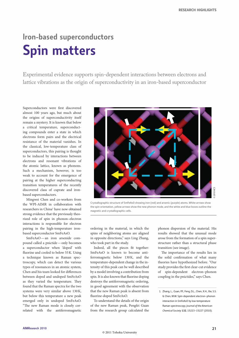
Superconductors were first discovered almost 100 years ago, but much about the origins of superconductivity itself remain a mystery. It is known that below a critical temperature, superconduct-ing compounds enter a state in which electrons form pairs and the electrical resistance of the material vanishes. In the classical, low-temperature class of superconductors, this pairing is thought to be induced by interactions between electrons and resonant vibrations of the atomic lattice, known as phonons. Such a mechanism, however, is too weak to account for the emergence of pairing at the higher superconducting transition temperatures of the recently discovered class of cuprate and iron- based superconductors.
Mingwei Chen and co-workers from the WPI-AIMR in collaboration with researchers in China1 have now obtained strong evidence that the previously theo-rized role of spin in phonon–electron interactions is responsible for electron pairing in the high-temperature iron-based superconductor SmFeAsO.
SmFeAsO — an iron arsenide com-pound called a pnictide — only becomes a superconductor when ‘doped’ with fluorine and cooled to below 55 K. Using a technique known as Raman spec-troscopy, which can detect the various types of resonances in an atomic system, Chen and his team looked for differences between doped and undoped SmFeAsO as they varied the temperature. They found that the Raman spectra for the two systems were very similar above 130 K, but below this temperature a new peak emerged only in undoped SmFeAsO. “The new Raman mode is closely cor-related with the antiferromagnetic
ordering in the material, in which the spins of neighboring atoms are aligned in opposite directions,” says Ling Zhang, who took part in the study.
Indeed, all the pieces fit together: SmFeAsO is known to become anti-ferromagnetic below 130 K, and the temperature-dependent change in the in-tensity of this peak can be well described by a model involving a contribution from spin. It is also known that fluorine doping destroys the antiferromagnetic ordering, in good agreement with the observation that the new Raman peak is absent from fluorine-doped SmFeAsO.
To understand the details of the origin of the new Raman peak, Pengfei Guan from the research group calculated the
phonon dispersion of the material. His results showed that the unusual mode arose from the formation of a spin super-structure rather than a structural phase transition (see image).
The importance of the results lies in the solid confirmation of what many theories have hypothesized before. “Our study provides the first clear-cut evidence of spin-dependent electron–phonon coupling in the pnictides,” says Chen.
1. Zhang, L., Guan, P.F., Feng, D.L., Chen, X.H., Xie, S.S.
& Chen, M.W. Spin-dependent electron–phonon
interaction in SmFeAsO by low-temperature
Raman spectroscopy. Journal of the American
Chemical Society 132, 15223–15227 (2010).
Crystallographic structure of SmFeAsO showing iron (red) and arsenic (purple) atoms. White arrows show
the spin orientation, yellow arrows show the new phonon mode, and the white and blue boxes outline the
magnetic and crystallographic cells.
Iron-based superconductors
Spin mattersExperimental evidence supports spin-dependent interactions between electrons and lattice vibrations as the origin of superconductivity in an iron-based superconductor
© 2
010
ACS
© 2011 Tohoku University

RESEARCH HIGHLIGHTS
22 AIMResearch 2010
Spintronics is a promising alternative to conventional electronics: the use of an electron’s spin instead of its electri-cal charge offers a relatively easy and energy-efficient way of manipulating information. Unfortunately, these spins don’t travel very far without the informa-tion they carry being destroyed. A new class of materials known as topological insulators could offer a solution to this problem by allowing almost unhindered spin transport, but owing to fabrica-tion and materials issues, none of the topological insulators known so far have clearly demonstrated this ability. Researchers from the WPI-AIMR and the Department of Physics at Tohoku University, in collaboration with col-leagues from Osaka University, have now discovered a material that could alleviate such problems1.
As their name suggests, topological insulators have to be electrically insulat-ing — that is, have an energy gap in their electronic states that electrons cannot overcome. Their unique properties arise on the surface, where they are electrically conducting. These conducting surface states are topologically protected, which means that electron spins are protected from degradation by, for example, the presence of impurities in the material.
So far, only a limited number of topo-logical insulators have been discovered, among them Bi2Se3. The problem with virtually all of the existing compounds is that their energy gap is too small, and so they are in fact electrically conducting in the bulk. The researchers have now discovered a new topological insula-tor, TlBiSe2. They found that the use of thallium considerably widens the band gap, leading to a topological insulator
with the largest known energy gap. The existence of protected surface states was confirmed by the tell-tale crossing of surface electronic states (pictured). “The enhanced material properties of this compound strengthen the foundation for high-speed, low-power consump-tion devices powered by topological insulators,” says Seigo Souma from the research team.
Like most other topological insula-tors, the samples fabricated from this compound are still electrically conducting throughout. According to Souma, this most likely results from mismatches in sample composition, and could potentially be solved by tuning the ratio of thallium and bismuth in the samples. The quality of the samples
prepared is sufficient to allow the precise investigation of their properties using the ultrahigh-resolution angle resolved photoemission spectrometer (ARPES) installed at Tohoku University. In any case, the insight gained in this study will also aid the search for new, related topological insulators, says Souma. “The discovery of a topological insulator in this TlBiSe2 ternary compound indicates considerable potential for the discovery of further topological insulators.”
1. Sato, T., Segawa, K., Guo, H., Sugawara, K., Souma,
S., Takahashi, T. & Ando, Y. Direct evidence for
the Dirac-cone topological surface states in the
ternary chalcogenide TlBiSe2. Physical Review
Letters 105, 136802 (2010).
The tell-tale crossing of electronic states in TlBiSe2 is evidence of the protected surface states.
Left: experimental ARPES intensity data (k, electron momentum). Right: three-dimensional theoretical model.
EF
0.2
0.4
0.6
0.8
High
Low–0.10 0.0 0.10
ky
kx
Bind
nig
ener
gy (e
V)
ky (Å–1)
Topological insulators
A large leap aheadThe discovery of a topological insulator with a large band gap suggests that room-temperature operation is possible for these promising spintronic materials
© 2
010
APS
© 2011 Tohoku University

RESEARCH HIGHLIGHTS
23AIMResearch 2010
Superconductors are of significant technological as well as scientific inter-est. Their ability to transport electri-cal current without resistance could provide significant energy savings, yet the known superconductors only dis-play their superconducting properties at temperatures close to absolute zero. Although the recent discovery of a ‘high-temperature’ class of superconductors, which despite their name only become superconducting below 100 °C, suggests that room-temperature superconductiv-ity might one day be possible, scientists still do not understand their physics suf-ficiently well to raise the zero-resistance transition temperature of these com-pounds significantly.
Returning to the classical, low-temper-ature superconductors, researchers from the WPI-AIMR in collaboration with colleagues from Hiroshima University and Yamaguchi University in Japan have now unveiled the possibility of increasing the transition temperature by judicious design of the material’s crystal structure1.
There are fundamental differences be-tween the mechanisms of superconduc-tivity in classical and high-temperature superconductors. In the classical case, su-perconductivity arises from the interac-tion between electrons and vibrations of the crystal lattice, known as phonons. In the high-temperature case, superconduc-tivity is thought to arise through interac-tions between the electrons themselves, mediated by their magnetic properties.
The classical superconductors studied by the researchers have a clathrate crystal structure (pictured) formed by a network of silicon or germanium cages that encap-sulate barium guest atoms. The barium guests are free to ‘rattle’ within the cage,
producing a particular type of phonon that can interact strongly with electrons. “The rattling motions in these cage mate-rials are currently drawing attention as a possible way to increase superconducting temperatures,” says Katsumi Tanigaki from the research team.
The researchers revealed the influ-ence of the cages on superconductivity through a detailed comparison between the properties of two clathrates, Ba24Si100 and Ba24Ge100, both of which are su-perconductors below their transition temperature. Of the two compounds, Ba24Ge100 has the larger cage and thus the stronger rattling motion. It would therefore be expected that it also has the higher transition temperature — but this is not the case. Its cage structure, it turns out, is too weak and distorted, which
degrades its superconducting properties.In principle, the findings point to the
possibility of enhanced properties. “Our work suggests that a higher supercon-ducting temperature may be realized if sufficiently strong cage materials can be designed,” comments Tanigaki. While the transition temperatures of clathrate superconductors are low at present, tun-ing the design of their cage structure may lead not only to higher superconducting temperatures in clathrates, but also to new strategies to improve other classical superconductors.
1. Tang, J., Xu, J., Heguri, S., Fukuoka, H., Yamanaka,
S., Akai, K. & Tanigaki, K. Electron–phonon
interactions of Si100 and Ge100 superconductors
with Ba atoms inside. Physical Review Letters
105, 176402 (2010).
The three-dimensional clathrate structure of Ba24
Si100
and Ba24
Ge100
. Both clathrates have the same polyhedral
network characterized by a framework of pentagonal dodecahedra embedded in a three-dimensional channel
labyrinth. The larger cage of the Ge100 clathrate allows the guest barium atoms to rattle more freely.
Superconductors
A sound solutionThe vibrations of atoms in cage structures point to a strategy to increase the transition temperature of superconductors
© 2011 Tohoku University

RESEARCH HIGHLIGHTS
24 AIMResearch 2010
Gold prices have skyrocketed in the past few years, but a study by research-ers from the WPI-AIMR and others at Tohoku University1 promises to make this precious metal even more valuable. Naoki Asao, Yoshinori Yamamoto and their co-workers have found that nano-porous gold — a material produced by selectively leaching silver atoms from a gold–silver alloy film — can catalyze an important step in the production of silicon-based polymers under milder and ‘greener’ conditions than those re-quired in conventional methods.
In its bulk state, gold has a familiar luster that doesn’t tarnish or discolor because it is chemically unreactive. At the nanoscale, however, the confined electrons of gold atoms can begin to os-cillate together, imparting new colors to the metal. “When we make nanoporous gold with pores around 100 nanometers in size, it has a reddish gold color,” says Asao. “As the pore size becomes smaller, the color becomes deeper, clearly indi-cating a change in electronic properties from the original thin gold film.”
This altered electronic behavior of nanoscale gold also makes it an active catalyst: gold nanoparticles supported on a solid substrate are known to cata-lyze a variety of reactions, providing an alternative to many toxic reagents in in-dustrial processes. Unfortunately, these materials suffer from a limited lifespan: eventually, gold nanoparticles agglomer-ate on the surface of the solid support and lose their reactivity. In light of this issue, attention has recently turned to nanoporous gold films.
The researchers investigated the catalytic performance of nanoporous gold for the oxidation of organosilanes,
which contain silicon–hydrogen bonds (see image). On oxidation, a hydrogen atom on the silicon center is replaced by a hydroxyl group, making the molecule easier to combine into silicon-based polymers. However, the reactions typi-cally used to achieve this result do not oxidize certain substrate types, tend to produce unwanted byproducts, or in-volve lengthy post-treatment processing.
The researchers found that immers-ing the nanoporous gold film in an aqueous organosilane solution at room temperature catalyzed the oxidation of silicon–hydrogen bonds with nearly quantitative efficiency. Furthermore, the catalyst was easily recovered and reused several times with no change in either reactivity or its nanopore structure.
The researchers are now investigating the mechanisms of nanoporous gold catalysis, and expect that this approach will have a major impact in the field of sustainable chemistry. “We believe that nanoporous gold will be useful for molecular transformations of natural gas and bioethanol for green chemis-try,” says Asao. “Nanoporous materials chemistry will surely develop much more in the future.”
1. Asao, N., Ishikawa, Y., Hatakeyama, N., Menggen-
bateer, Yamamoto, Y., Chen, M., Zhang, W. &
Inoue, A. Nanostructured materials as catalysts:
Nanoporous-gold-catalyzed oxidation of
organosilanes with water. Angewandte Chemie
International Edition 49, 10093–10095 (2010).
A nanoporous gold substrate can catalyze the oxidation of organosilane compounds at room temperature,
providing a promising alternative to existing reagents.
Nanostructured catalysts
Golden openingsThin gold sheets with nanoscale pores act as durable and reusable green catalysts
© 2
010
Wile
y-VC
H
© 2011 Tohoku University

RESEARCH HIGHLIGHTS
25AIMResearch 2010
In contrast to most metals in which atoms are arranged in a repeated crystal pattern, the atoms in metallic glasses do not have long-range order. This gives them certain desirable characteristics, including resistance to wear and corro-sion, and high strength. The continued improvement of metallic glasses would benefit greatly, however, from a detailed understanding of their atomic structure.
Various atomic models for metallic glasses exist, yet none have been con-firmed because the experimental char-acterization of metallic glasses has been limited to the acquisition of average data over relatively large volumes. Now, in a collaboration between the WPI-AIMR and the Institute for Materials Research at Tohoku University, Osaka University in Japan and the Grenoble Institute of Technology in France, Mingwei Chen, Akihiko Hirata and colleagues have characterized the atomic structure of metallic glasses with unprecedented resolution by combining ‘nanobeam’ electron diffraction with molecular dy-namics simulations1.
The researchers began by character-izing the metallic glass Zr66.7Ni33.3 using standard electron diffraction and elec-tron microscopy tools. As expected, no diffraction spots were observed, indicat-ing a lack of regular atomic order, and no order could be detected by electron microscopy. Unsatisfied with the find-ing, Chen, Hirata and their co-workers began work to make the electron beam narrower in order to resolve finer atomic structures. By correcting for spherical aberrations in their electron optics and using a specially designed electron beam condenser aperture, they were able to reduce the diameter of their electron
beam to about 3 angstroms (Å) or 0.3 nanometers, the narrowest coherent electron beam demonstrated so far.
This much narrower beam produced a distinct set of diffraction spots (pictured) that could only result from a single crys-tal, confirming predictions that metallic glasses are composed of small ordered atomic clusters as fundamental struc-tural units, even though these materials are disordered on larger scales. By scan-ning their narrow beam around their sample and using a low-power beam to avoid damaging the atomic structure, the team was able to sample hundreds of ordered clusters, each about 4–7 Å in size. The data showed that the average atomic spacing inside an ordered atomic cluster was 2.4 Å. A molecular dynamics
numerical model reproduced key fea-tures of the experimentally measured diffraction pattern, confirming that local order was indeed being observed.
According to Chen, this work could have consequences in both research and applications of metallic glasses. “We can now begin to propose a reliable atomic structure model for new metallic glass design, aiming for better forming ability and a better understanding of important physical processes such as glass transi-tion and deformation,” he says.
1. Hirata, A., Guan, P., Fujita, T., Hirotsu, Y., Inoue,
A., Yavari, A.R., Sakurai, T. & Chen, M.W. Direct
observation of local atomic order in a metallic
glass. Nature Materials 10, 28–33 (2011).
A typical narrow-beam electron diffraction pattern for the metallic glass Zr66.7
Ni33.3
. The distance to the spot A
can be used to model the short-range atomic order.
A
Metals
Bringing glass to orderDiffraction patterns obtained using an electron beam only a few angstroms wide have revealed local order in otherwise amorphous metallic glasses
From
Ref
. 1. ©
201
0 M
.W. C
hen
© 2011 Tohoku University

RESEARCH HIGHLIGHTS
26 AIMResearch 2010
Thin oxide films are used in applications ranging from solar cells to transistors. They are made useful in part by the abil-ity to tune many of their key properties, including conductivity and transpar-ency. Some oxides can be changed from highly insulating to highly conductive by altering their structure or ‘doping’ them with foreign atoms. Zhongchang Wang and co-workers in the laboratories of Yuichi Ikuhara and Masashi Kawasaki at Tohoku University’s WPI-AIMR in collaboration with researchers from the University of Tokyo and the Japan Fine Ceramics Center have now demon-strated a counter-intuitive way to induce an oxide to become conductive1.
The research team studied the con-ductivity of a thin film of a layered oxide composed of lanthanum, strontium and titanium. Using pulsed laser deposition, they were able to construct the film one atomic layer at a time with control over the nature of each layer. They focused on examining the effects of inserting insulating layers of SrTiO3 — a ceramic commonly used in electronic applications. Surprisingly, they found that the oxide underwent a transition from insulating to conductive behavior when a higher density of the insulating layers was included. This conductiv-ity appeared without any change in the density of charge-carrying electrons, showing that the state was not the result of doping — a standard technique for raising conductivity.
Wang and his colleagues investigated the effect of inserting the additional insulating layers using a combination of scanning electron microscopy (micro-graph pictured) and numerical simula-tions. Their studies showed that the
addition of the insulating layers reduced distortion and bond strain in the oxide film. Distortion and strain can lead to insulating states by affecting the inter-actions between the electrons and the lattice, as well as the interactions among the electrons themselves. By allowing the material to relax to a less-strained state, the researchers were able to increase its conductance. Their data show that this counter-intuitive behavior arises from the creation of a conductive two-dimensional layer inside the oxide.
The results represent a new route to obtaining metallic behavior in materi-als that are normally expected to be insulators. The research team expects their finding to accelerate the search for
superconducting and thermoelectric materials in oxides and other insulating materials. “Our first priority now is to consider whether superconductivity can be elicited in this particular oxide by reducing lattice disorder and struc-tural defects so as to lower the barrier to charge carrier motion,” says Wang. The researchers believe that the material may also find use in high-mobility transistor and thermoelectric applications.
1. Wang, Z., Okude, M., Saito, M., Tsukimoto, S.,
Ohtomo, A., Tsukada, M., Kawasaki, M., Ikuhara, Y.
Dimensionality-driven insulator–metal transition
in A-site excess non-stoichiometric perovskites.
Nature Communications 1, 106 (2010).
Scanning transmission electron microscopy image of the layered oxide film. Bright spots represent strontium,
and dimmer spots correspond to titanium.
5 Å
Oxides
Less is moreInserting insulating layers into an oxide can make it more conductive
© 2011 Tohoku University

IN THE SPOTLIGHTThe WPI-AIMR has grown rapidly since its inauguration in 2007, now with over 100 leading researchers from all over the world, including 32 internationally renowned Principal Investigators who are charged with pioneering new and innovative break-throughs in materials science. The institute is also active in developing young, promising researchers with a focus on strong cross-disciplinary collaboration and creativity. AIMResearch spotlights these talented researchers of the present and future, detailing their daily research activities and scientific ambitions.
© 2011 Tohoku University

IN THE SPOTLIGHT
28 AIMResearch 2010
DIRECTOR’S INTERVIEW
Time to shake things upAs the WPI-AIMR celebrates its third anniversary in October 2010, Director Yoshinori Yamamoto shares his vision for the institute’s future.
T he WPI-AIMR first opened its doors in 2007 as one of the first of five World Premier International
research centers to be created under a new initiative of the Ministry of Education, Culture, Sports, Science and Technology of Japan and administered by the Japan Society for the Promotion of Science. The WPI-AIMR has successfully navigated its first three years of life. Now, having estab-lished itself as a leading center of materials research in Japan and with a growing international reputation, attention within the WPI-AIMR is turning to the next phase of development. AIMResearch talked to the institute’s director, Yoshinori Yamamoto, an internationally renowned chemist, about the successes and chal-lenges of his three years at the helm and the path that he has laid out for the future direction of the institute.
The WPI-AIMR has a broad and interdisci-plinary remit. What do you think stand out as the institute’s biggest achievements to date?
The WPI-AIMR program has two main objectives: one is to develop new in-novative materials through the fusion of research, and the other is to establish a new management system that best suits WPI-AIMR. However, achieving these objectives is not so easy.
We have research groups working in bulk metallic glasses, materials physics, soft materials and devices/systems and all of them have made great progress over the last three years. In bulk metallic glasses, for instance, we have published a paper about the controlled formation of metallic glass nanowires in Advanced Materials1. Nanowires are useful materials for a wide
range of applications and we were the first to make metallic glass nanowires. In materials physics, we have published a paper concerning the mechanism behind superconductivity in Europhysics Letters2.
We have the most powerful angle-resolved photoemission spectrometer in the world and we used it to show that electron spin plays an important role in superconductivity. The paper has so far received more than 300 citations. In soft materials, we are making nanoporous pal-ladium catalysts. In devices/systems, we are investigating the use of bulk metallic glasses as soldering materials in micro-electromechanical systems.
Setting up the center and guiding it through its initial phase could not have been easy. What were some of the chal-lenges and how did you overcome them?
Asking researchers to jump outside their own research discipline was quite
a challenge. On the one hand, senior researchers prefer to stay in the same discipline especially when they have estab-lished a presence in the community. On the other hand, young researchers want to establish their own discipline before they venture into something new. I think a good researcher should have a wide view of science, no matter how challenging it may be. At the WPI-AIMR, I often see young researchers jumping between labo-ratories. There is extensive collaboration going on and I think this is a very good thing. However, the fusion of research is much bigger than just collaboration. I hope that in the near future, our research-ers will go beyond collaboration and create some entirely new science.
Reforming our management system was another challenge. Most principal investigators in Japan believe in equality — everyone should get the same area of space, hire the same number of research-ers and receive the same salary. Here at the WPI-AIMR, everything depends on achievement. If your results are excellent, you can hire more people and get more space. Such a management model is very rare in Japan, but I think it suits the WPI-AIMR very well.
A key part of the WPI Initiative is the globalization of research. What plans do you have for strengthening international collaboration?
Internationally, we have been collaborat-ing with the University of Cambridge in the UK in bulk metallic glass research. We have also started collaborating with the Institute of Chemistry, Chinese Academy of Sciences (ICCAS) in materials research.
WPI-AIMR Director Yoshinori Yamamoto would like to see more mixing among WPI-AIMR researchers.
Published online 25 October 2010
© 2011 Tohoku University

IN THE SPOTLIGHT
29AIMResearch 2010
The WPI-AIMR is strong in materials physics, while the ICCAS is strong in ma-terials chemistry. I think this collaboration will benefit us both.
Earlier this year the WPI-AIMR was evalu-ated by a follow-up committee to assess the progress of the project. What were their key findings and advice?
Every year, we need to report the progress of the WPI-AIMR program to a follow-up committee. This year, the program direc-tor and members of the working group of the follow-up committee carried out a two-day site visit at the WPI-AIMR. They submitted a very detailed report to upper committee members from Europe, the United States and Japan. In July, we had a meeting with the upper committee members in Tokyo. We gave a 15-minute presentation and the upper committee members posed some very serious ques-tions and gave some valuable advice. For
example, they said that our quality of science is excellent. However, they also said that there is room for improvement in promoting the fusion of research and global visibility.
The WPI-AIMR will enter its second phase in 2012. What plans does the WPI-AIMR have for the future?
We have set a roadmap for the WPI-AIMR program. In April next year, the construction of the WPI-AIMR main building will be completed. Then in October, we will have an interim evalua-tion. This is a very important time as we will re-evaluate the directorship, the prin-cipal investigators and all researchers, and make any changes that may be necessary. We will also focus our research on the de-velopment of innovative materials, as we have mentioned in our mission statement. In 2017, the WPI-AIMR will enter its third phase. By then, the university must
establish a new organization based on in-novative materials discovered through the WPI-AIMR program.
How will the WPI-AIMR’s new building, to be completed in April 2011, help with the research program?
Right now, some of our researchers are working in Aobayama campus. They will all move to the new building at Katahira campus once the new building is ready. To do fusion research, the researchers must stay in the same building. The building is sort of like a beaker, and my job is to shake things up.
1. Nakayama, K.S., Yokoyama, Y., Ono, T., Chen, M.W., Akiyama, K., Sakurai, T. & Inoue, A. Advanced Materials 22, 872–875 (2010).
2. Ding, H., Richard, P., Nakayama, K., Sugawara, K., Arakane, T., Sekiba, Y., Takayama, A., Souma, S., Sato, T., Takahashi, T., Wang, Z., Dai, X., Fang, Z., Chen, G.F., Luo, J.L. & Wang, N.L. Europhysics Letters 83, 47001 (2008).
TECHNOLOGY FOCUS
MEMS technology makes the world a merrier placeScientists at the WPI-AIMR have developed microelectromechanical systems for a wide variety of applications, ranging from microphones for television studios to automobiles and airport surveillance equipment.
M icroelectromechanical systems (MEMS) are miniature devices containing both electrical and
mechanical components. The technology is an application of microfabrication for integrated circuits and draws together expertise in mechanics, optics and materi-als. “We call this heterogeneous integra-tion,” says Masayoshi Esashi, a principal investigator at Tohoku University’s WPI-AIMR — he is also a global authority on MEMS technology. “By merging different technologies together, we can produce
value-added MEMS devices with impor-tant core functionality in many systems.”
Tiny devices, large applicationsEsashi first encountered MEMS when he was an engineering student at Tohoku University in the early 1970s, and has spent the last 40 years working in the field. In his career, he has developed tech-nologies for numerous MEMS devices that have become integral parts of our daily lives. Video game controllers, inkjet print-ers, digital cameras and automobiles are all
Esashi is the pioneer of MEMS technology and a global authority in the field.
Published online 28 June 2010
© 2011 Tohoku University

IN THE SPOTLIGHT
30 AIMResearch 2010
examples of applications utilizing MEMS technology in some form or another.
“For example, a Nintendo Wii remote controller has a MEMS accelerometer that captures motion, which allows us to control the user interface and enjoy the game,” explains Esashi. “And one printer produced by Canon incorporates a MEMS print head with 6,000 nozzles for emitting small ink droplets, which allows it to print high-resolution images.”
Some of Esashi’s latest MEMS cre-ations include an angular motion sensor developed in collaboration with Toyota researchers that detects any rotation of the car and compares it with the expected speed and angle of steering. When the sensor detects an unexpected spin situa-tion, it automatically applies the brakes. Other transport-related applications for Esashi’s MEMS sensors included a two-dimensional optical scanner that is used in security surveillance equipment at Tokyo’s Haneda International Airport and at railway stations.
Advantest, the world’s largest semi-conductor testing company, is also using Esashi’s MEMS switches in their latest large-scale integration (LSI) testers as a replacement for conventional switches based on electronic transistors, which are susceptible to electrostatic damage. The new MEMS switches are not affected by electrostatic discharge, making the LSI testers much more reliable. Elsewhere, the Japanese television channel NHK is using Esashi’s MEMS microphones in environments with particularly high humidity, such as in television studios for recording cooking programs.
Another important potential applica-tion for MEMS technology is in mag-netic resonance imaging (MRI). “We have developed a thin cantilever holding an iron particle for detecting extremely weak magnetic resonance signals. It is used by the Japanese instrument maker JEOL,” explains Esashi. “They are using it for electron spin resonance imaging on micrometer-sized samples, which will enable the real-time visualization of the effects of medicine on cells.”
Small has its advantageIn addition to their small size, MEMS offer many advantages over conventional electromechanical devices. Esashi can make very small devices that provide extremely high sensitivity or spatial reso-lution, using extended microfabrication technology and at a fraction of the cost of conventional LSI devices.
“LSI fabrication typically involves the use of a photomask for transferring tran-sistor patterns onto the silicon wafer. The mask can be very expensive, up to ¥500 million [US$5 million],” notes Esashi. “Therefore, such advanced technology is only viable for mass-production applica-tions. For small-volume production, we are developing a MEMS-based maskless electron-beam exposure system, in which an electron beam is used to draw the transistor pattern on the wafer. The technology reduces costs and increases controllability, accuracy and versatility.”
Acting as the bridgeEsashi believes that the future of MEMS lies in collaboration among academics and multiple commercial stakehold-ers — what he terms ‘company + company + university collaboration’ — and refocus-ing efforts on practical applications.
“We would like to support the indus-try by establishing a platform on which people can come together to work. We educate the researchers from companies. They learn, and then they go back to their companies to commercialize the technol-ogy, in many cases through inter-com-pany collaboration. This is our way to contribute to society indirectly,” he says.
Esashi’s laboratory currently has 40 full-time researchers, including research-ers from six companies of the likes of Fuji Film. His aim is to bridge the gap between pure research and application, while retaining the challenge and curi-osity of scientific investigation. Within the WPI-AIMR, Esashi promotes joint research with the institute’s bulk metal-lic glasses group on MEMS bonding technology with metallic glass and nano-structured metals.
“Our facilities are like toys. They are home-made instruments, giving re-searchers the chance for a fundamental experience not replicable in a company. If the researchers succeed in making de-vices using such equipment, they find it very rewarding and a lot of fun. This is very important for the researchers.”
Esashi at his MEMS fabrication unit. His distinctive red cleansuit was given to him by his students to celebrate his 60th birthday.
MEMS on a chip
© 2011 Tohoku University

IN THE SPOTLIGHT
31AIMResearch 2010
T he WPI-AIMR Annual Workshop is a key date in the yearly calendar of the WPI-AIMR when the
members of the center join together with other notable researchers from around the globe to discuss the latest developments in materials science, exchange information and ideas, and look towards the future.
The 2010 Annual Workshop — the third in the series — was held from March 25 in the city of Sendai in Japan’s northerly Miyagi prefecture, the base of the WPI-AIMR. The 2010 meeting was attended by more than 220 researchers from 17 countries, including many senior and in-ternationally renowned materials scientists from Asia, Oceania, Europe and North America, who braved the unseasonably low temperatures to engage in three days of wide-ranging discussion and debate.
In his welcoming address, WPI-AIMR Director Yoshinori Yamamoto encouraged all participants to attend as many different sessions as possible over the duration of the workshop. He also pointed out that the guiding principle of the WPI-AIMR is ‘fusion research’, and that the organization of the lecture program into several parallel sessions dealing with a mixture of topics including bulk metallic glasses, nanophys-ics, nanochembio and devices & systems was a conscious effort by the organizers to reflect the center’s mission and encourage cross-disciplinary thinking.
The wide variety of parallel sessions were designed to supplement a program of 18 plenary talks given by leading in-ternational materials science researchers, including WPI-AIMR members based at institutions outside Japan. In addition, the poster session held on the afternoon of Friday March 26 drew close to 80 poster
presentations on a wide variety of topics that were the subject of vigorous debate among the participants.
The workshop also witnessed the presentation of the 2010 Acta Materialia Gold Medal to Akihisa Inoue, president of Tohoku University and an International Advisory Board member at the WPI-AIMR. First awarded in 1974, the prize is given annually by Acta Materialia Inc. to honor a researcher who has made a con-tribution of particular merit to materials science. Inoue is only the third Japanese researcher to receive the award, and the second from Tohoku University. The award, which was made in recognition of Inoue’s pioneering work on bulk metallic glasses and outstanding achievements and leadership in materials science, was presented by Ted B. Massalski (Carnegie Mellon University), the Executive Secretary of Acta Materialia, at a ceremony in the Sendai International Center.
One of the focal points of the workshop
was a special Nobel Laureate Lecture in which Georg Bednorz, who was awarded the 1987 Nobel Prize for Physics for his work on high-temperature superconduc-tivity, gave a wide-ranging talk on the topic of ‘Exploring the Nanotechnology Landscape’, drawing on his work at the IBM Zurich Research Laboratory. Speaking to AIMResearch, Bednorz, a member of the WPI-AIMR International Advisory Committee, praised the work of the center: “Last year I attended the [WPI-AIMR] workshop and I found the activities here to be quite amazing,” he said, particularly noting that the work of the center encompasses “quite a broad spectrum of activities.” Bednorz also described the fusion research approach as being “very important” and praised the WPI-AIMR policy of giving young researchers a free hand in directing their research. “I think it’s important that young people take the initiative … they get financial support and take over a common project. I think this is important,” he said.
Yamamoto also spoke to AIMResearch
INTERNATIONAL WORKSHOP
Fusion research on the global stage25–27 March 2010: The World Premier International Advanced Institute for Materials Research (WPI-AIMR) held its third WPI-AIMR Annual Workshop in Sendai, Japan.
WPI-AIMR Director Yoshinori Yamamoto welcomes participants to the 2010 WPI-AIMR Annual Workshop
Akihisa Inoue (right) receives the 2010 Acta Materialia Gold Medal
Published online 26 April 2010
© 2011 Tohoku University

IN THE SPOTLIGHT
32 AIMResearch 2010
M any scientists focus their research on making new materials, but tend to lose
sight of novelty and the environment. Supercritical fluid technology opens a new world of possibilities in making hybrid materials with multiple functions without relying on hazardous chemicals.
Every fluid has a critical point — a specific combination of temperature and pressure above which the liquid and gas phases disappear and are replaced with a ‘supercritical fluid’ phase.
Supercritical fluids have many un-usual properties, such as high density and low viscosity, which make them ideal
for use as solvents, as Tadafumi Adschiri — a principal investigator at Tohoku University’s WPI-AIMR and a global leader in supercritical fluids — points out. “We can tune the density of a supercriti-cal fluid through small changes in tem-perature or pressure,” he says. “Because solubility and phase behavior are a direct function of density, we could mix a supercritical fluid, such as water, with many things that are normally immiscible or insoluble, such as oil or hydrogen gas.”
Supercritical fluids have many usesAdschiri has been using supercritical fluids for the synthesis of inorganic
Tadafumi Adschiri is a global leader in supercritical fluids
about the importance of fusion research, and confirmed his commitment to keep it at the heart of the scientific activities of the center. “The WPI-AIMR is now in its third year, and we feel that we have finally established the right organizational and research structure that will allow us to go forward,” he said. “We have already made a number of interesting discoveries and now we can accelerate the pace of deliv-ery. The concept of fusion research will be critical in realizing this goal.”
Himself a longstanding proponent of increased participation of overseas researchers in Japanese institutions, Yamamoto commented favorably on the international diversity of the workshop. This is reflected in the makeup of the WPI-AIMR personnel, in which one-third of the academic staff and almost two-thirds of the research associates are non-Japanese, a fact that Yamamoto iden-tified as being one of the key strengths of the center. This success is a result
of a conscious and sustained policy of proactively recruiting talented young re-searchers from overseas to work alongside Japanese counterparts, he noted. “We are now in the happy position of actually getting unsolicited enquiries from young foreign scientists asking us about research opportunities at the WPI-AIMR,” com-mented Yamamoto. “We expect that in the near future, young people from all over
the world will come to see the WPI-AIMR as a natural choice for advancing their re-search career in materials science.”
The very high level of science on dis-play at the 2010 WPI-AIMR Annual Workshop and the obvious enthusiasm of the many young international partici-pants would seem to suggest that this am-bition may well be realized sooner rather than later.
TECHNOLOGY FOCUS
Mixing the unmixableThe synergy of different expertise and ideas helps advance the development of ‘super’ hybrid materials.
The audience at the third WPI-AIMR Annual Workshop
Published online 30 August 2010
© 2011 Tohoku University

IN THE SPOTLIGHT
33AIMResearch 2010
nanocrystals, which have a vast number of potential uses in industry but which are usually prepared using harsh chemi-cals. So far he has made nanocrystals of various metal oxides, including titanium dioxide, zirconium oxide and selenium oxide, as well as double-metal oxides such as barium titanate and barium fer-rite. “There are many methods for syn-thesizing nanocrystals, but there are several problems. One problem is the use of organic solvents, which are hazardous to the environment. Another problem is low productivity.”
Adschiri has been able to increase the productivity of synthesis by growing the nanocrystals in supercritical water, avoiding the use of hazardous chemicals. Furthermore, as supercritical water mixes with oil, Adschiri can synthesize novel organic–inorganic hybrid nanocrystals — a feat that could not be achieved using conventional methods.
“Many people can make inorganic nanocrystals, but they have difficulty dispersing these nanocrystals in poly-mers or organic solvents. We can make nanocrystals with organic molecules on the surface, which have high affinity with plastic polymers and organic solvents, and then transplant them into polymer films. We can also tune the properties of the polymers very easily.”
A super filmmakerUsing his unique nanocrystals, Adschiri is developing a range of nanocrystal–polymer hybrids, including a transpar-ent film with high refractive index. The plastic film rolls up just like any normal plastic film, but its high refractive index could be useful for manufacturing thin-ner optical lens and anti-reflective coat-ings. “You cannot see the particles, but they give the film a very high refractive index,” says Adschiri.
Another hybrid film he is developing is a plastic film consisting of over 90% boron nitride particles. The hybrid mate-rial has high thermal conductivity but low electrical conductivity — normally in-compatible properties — and can be used as a heat-transfer material for cellular phones, computers and other electronic devices. In collaboration with other WPI-AIMR researchers, Adschiri is also work-ing on a plastic film containing magnetic particles, which he believes could be use-ful for making polarizers and photonic tuners. “We call these novel hybrid mate-rials ‘super hybrid materials’ because they have multiple, normally incompatible properties,” he says.
A mix of ideasAdschiri opened his laboratory eight years ago, and at that time, he already foresaw the importance of working with research-ers from completely different fields. “I was
working in the field of supercritical fluids, but to explore new materials, I needed people who had different viewpoints. I had three positions in the laboratory, so I invited a biochemist, a material scientist and a computer scientist to join,” he says.
In the beginning, the four original members of the team did not have a common scientific background. But they spent half a year explaining their ideas to each other from a basic graduate level and eventually found a direction they all could follow — the combination of nanoparticles, polymers and biomaterials, brought together with simulations of the underlying physics.
Adschiri now has 30 researchers, including ten postdoctoral researchers, working in his laboratory. His unique philosophy of fusing different expertise and ideas is still evident in the people he employs, and he remains undaunted by any perceived risk of working with people with such diverse backgrounds: “It’s a gamble, but I like a gamble,” he says.
Many companies are now interested in using organic and inorganic materials to make super hybrid materials. Looking forward, Adschiri has a clear vision for where he wants to take his group’s research on super hybrid materials: He intends to support the growth of this unique technology while exploring the creation of new materials through the fusion of ideas.
A transparent, high-refractive-index film based on nanocrystal–polymer hybrid technology
Tadafumi Adschiri and his co-workers use supercritical fluid technology to create new hybrid materials.
© 2011 Tohoku University

IN THE SPOTLIGHT
34 AIMResearch 2010
TECHNOLOGY FOCUS
From the bottom upResearchers in the Bulk Metallic Glasses Group at the WPI-AIMR are showing how fusion research can be used to understand the structure and properties of ‘atomic’ materials.
W hen asked to describe the toughest challenge facing him in his work, Mingwei Chen,
group leader and principal investigator of the Bulk Metallic Glasses Group, does not hesitate in reply: “Bulk metallic glass is an atomic-scale material. We still don’t know how the individual atoms are arranged. Understanding structure at the atomic level is the most important topic in this research,” he says.
First reported in the early 1960s, metallic glasses are a special type of metal alloy that promise to revolutionize the materials industry. Unlike conventional metals, which are produced by allowing the molten metal to cool slowly to afford a material with a well-ordered crystalline structure at the microscopic level, bulk metallic glasses (BMGs) are formed by rapid cooling of the bulk sample such that it solidifies without crystallization. The resulting metals are locked into a disor-dered ‘liquid-like’ structure, which means that they soften and flow at comparatively low temperatures allowing them to be molded and processed much more eas-ily than conventional metals. At the same time, the irregular, tightly packed internal arrangement of the atoms in BMGs gives them higher density, strength and resis-tance to wear and corrosion compared to many crystalline metals. Early BMGs had critical cooling rates — the rate of cooling required to create the characteristic amor-phous structure — on the order of one million degrees per second. More recent systems, some of which were discovered in the ‘80s and ‘90s at Tohoku University, the home of the WPI-AIMR, have much lower critical cooling rates, although the reasons behind this are still not clear. “Part
of our work focuses on some of the most fundamental issues in BMG research, such as the mechanism of BMG formation,” says Chen. “Why, for example, do some alloys have very low critical cooling rates and such good glass-forming ability? This is a big question in this area and we spend a lot of time and effort to understand this issue in my group.”
Deformation without crystallizationAnother important topic is the ques-tion of how BMGs can be plastically deformed. Although BMGs are typically several times stronger than conventional crystalline metals, they are not ductile at normal temperatures and have a tendency to fail abruptly when stretched, with no indication that failure is imminent. This limits their usefulness in load-bearing applications where structural reliability is critical. “Crystalline materials can be plastically deformed by the motion of dis-locations — a line of defects in the crystal lattice,” explains Chen. “BMGs are glassy and do not have a crystalline structure, yet we still observe plastic deformation in these systems.” To account for this phenomenon, Chen and his co-workers utilize and develop the theory of shear transformation zones (STZs), nano-sized pockets that undergo plastic deformation resulting in a build-up of stress and the formation of localized shear bands, which can eventually lead to mechanical failure of the BMGs. Examination of a series of different BMG systems using a new tech-nique called ‘rate-jump nanoindentation’ developed at the WPI-AIMR has made it possible to correlate the volume of the atomic clusters involved in the STZs with the ductility of the BMGs. “Unlike
conventional metals where we can gain information about the bulk properties of a sample by looking at its microstructure through a microscope, in the case of BMGs we have to examine the structure at the atomic scale in order to understand the material’s bulk mechanical properties. Once we have a clear understanding of this we can begin to design BMG systems with the desired atomic arrangement for improved mechanical properties,” he says.
Looking at the small pictureGetting down to this level of structural detail requires the deployment of cutting-edge experimental techniques such as extended X-ray absorption fine structure spectroscopy, which is carried out using the synchrotron radiation facility at the RIKEN SPring-8 center located at the Harima institute west of Kobe in central western Japan. Closer to home, Chen and
Mingwei Chen, leader of the BMG Group at the WPI-AIMR
Published online 28 February 2011
© 2011 Tohoku University

IN THE SPOTLIGHT
35AIMResearch 2010
his co-workers have also developed an angstrom beam electron diffraction tech-nique using a coherent electron beam with a width of approximately 0.3 nanometers to observe the arrangement of individual atomic clusters in a BMG sample. The high levels of precision required for the experiment were only possible thanks to a state-of-the-art, custom-made spheri-cal aberration-corrected transmission electron microscope, which was built in collaboration with a major Japanese scien-tific instrument manufacturer and which incorporates a condenser aperture de-signed by researchers at the WPI-AIMR. The electron microscope, purchased with strategic funding from the WPI-AIMR, is one of only a handful of such instruments in Japan and has generated interest from other researchers both inside and outside the WPI-AIMR.
Although he considers BMG as his main field and notes its position as one of the mainstays of the work of the WPI-AIMR, Chen is keen to stress that the Advanced Functional Materials Laboratory is concerned with much more than just BMG research. The remit of the section is broad — nanostructured materials, nanocomposites and nanocrys-talline metals for high-strength materials are all included in the portfolio, along with research into metal colloids and the theoretical studies and simulations that underpin concepts such as STZs. “We carry out a wide range of research here, but BMG research will always be a key topic for the WPI-AIMR, not just because of its inherent importance but also because Tohoku University has made a special contribution in this area,” says
Chen referring to the more than 40-year involvement of the university in the field of BMG research.
Fusion research, green innovationA key member of the original committee that proposed and subsequently set up the WPI-AIMR, Chen began his academic career as an associate professor at the prestigious Shanghai Jiaotong University in China before joining the Institute for Materials Research at Tohoku University as a guest researcher from 1997 to 1999. Following a stint in the US where he worked as an associate research professor at Johns Hopkins University, he returned to Sendai in 2003 to join the International Frontier Center for Advanced Materials as one of the first non-Japanese research-ers to be hired as a professor at Tohoku University. “One of the reasons I came back to Japan is because the equipment here is so good. Plus the research funding is much more stable than in other coun-tries such as the US,” he says. Chen also cites the strong teamwork ethic in Japan, which sees graduate students working closely with associate, assistant and full professors, as another positive point of working at Japanese institutions such as the WPI-AIMR.
As might be expected for one who has been intimately involved with the WPI-AIMR since its inception, Chen is an enthusiastic supporter of the concept of fusion research being pioneered at
the institute. Discoveries made by Chen and his co-workers in the Advanced Functional Materials Laboratory are already being applied in other groups of the WPI-AIMR. Nanoporous metal–ionic liquid composites, for example, which are being developed for electrocatalysis and super capacitors, have their origins in Chen’s laboratory, as do the nanoporous gold catalysts being used in chemical synthesis by the Soft Materials Group. Other products of BMG research are being taken up by microelectromechani-cal systems (MEMS) researchers in the Devices/Systems Group as materials for micro-mirrors in applications such as virtual retinal displays, virtual keyboards and mobile phone projectors. In addition to these applications, Chen foresees an increased emphasis on the development of functional applications for materi-als in the arena of green innovation, an endeavor in which fusion research will be even more important. “I come from a background of traditional physical met-allurgy, but now I am doing research in so many areas, from physics, chemistry and electrochemistry to energy-storage devices and biosensors. My research team all come from different backgrounds too: applied chemistry, applied physics, mechanics — the lot. Fusion research is absolutely essential for the work of the WPI-AIMR, and when you think about it, we’re actually doing fusion research within my own group,” he says.
Using the spherical aberration-corrected transmission electron microscope
Chen works on a number of topics in addition to BMG research
© 2011 Tohoku University

IN THE SPOTLIGHT
36 AIMResearch 2010
Since the WPI-AIMR first started in 2007, the institute has been bringing together researchers
from all over the world to work on new fields in materials science. AIMResearch speaks to four researchers who have made the plunge and moved to Japan to join the WPI-AIMR.
How did you discover the WPI-AIMR at Tohoku University here in Sendai, and what kind of research are you now involved in?
Ken Nakajima: After finishing my PhD in polymer physics at the University of Tokyo, I took a postdoctorate position at RIKEN and then joined the Tokyo Institute of Technology as an assistant professor. I was actually born in Sendai though, and Tohoku University is known as one of the best universities in Japan. I joined the Soft Materials Research Group at the WPI-AIMR and am now an associate professor.
Are you glad to be back in Sendai?
Nakajima: I am honoured to be here. The WPI-AIMR has a unique organizational structure that gives me many new chal-lenges. I get to work with many foreign re-searchers and they give me broad insights into science. I am now studying polymers and their mechanical properties using scanning probe microscopy (SPM).
Limei Xu: I came here by coincidence. I discovered the WPI-AIMR when some-one passed me an advertisement for the institute while at a conference in Europe. I knew the WPI-AIMR was the world’s lead-ing research institute in materials science. I thought it might be good chance to shift my research direction to materials science, so I immediately applied.
Was the transition difficult?
Xu: My PhD at the Center of Polymer Studies at Boston University involved using statistical physics to study critical phenomena in glasses and polymers. Now I am an assistant professor working in the Bulk Metallic Glass Research Group at the WPI-AIMR. Materials science was new to me and the transition from polymers to bulk metallic glasses (BMGs) was not straightforward. Before, my study was more fundamental and the models I developed were for general materials. Here at the WPI-AIMR, researchers work with very specific materials. It is very difficult for me as a theoretician to come up with a model that incorporates the properties of all the different kinds of materials.
Kazunori Ueno: I did my doctorate study at the National Institute of Advanced Industrial Science and Technology (AIST) in Tsukuba. Professor Masashi Kawasaki,
my boss now at the WPI-AIMR, was one of the principal investigators at AIST at that time. Because Tohoku University’s Institute for Materials Research is very famous for research in material sciences, I decided to join Kawasaki’s group at Tohoku University and do my postdoctor-ate here. Five years later, the WPI-AIMR was established, and I didn’t hesitate to join.
What was the attraction of the WPI-AIMR?
Ueno: The new Materials Science Research Group was very attractive for me as a young scientist. I am an assistant professor working in the Materials Physics Research Group, where I study oxide materials and ceramics, particularly their applications in semiconductor devices, su-perconductors and field-effect transistors. I am currently trying to combine ceramics with organic materials to create materials with new properties.
Doctor Caron, you were born in France? Why did you come to Japan?
Arnaud Caron: Yes, I was born in France. I came to Japan partly because of curiosity. I went to Germany to do postdoctoral study at the University of Ulm. Professor Hans-Jörg Fecht, my supervisor at that time, happened to be an adjunct professor at the WPI-AIMR. He suggested that I should apply for a position here. As a young researcher, I try to broaden my scope, and the WPI-AIMR is a very international institute where I get to interact with people from different fields and nationalities. I wanted to see something different to Europe and so I applied.
FEATURED RESEARCHERS
Learning the differenceAt the WPI-AIMR, researchers are beginning to understand each other’s strengths but there are still hurdles on the road to finding new functional materials.
“The WPI-AIMR has a unique organizational
structure that gives me many new challenges.”
KEn nAKAjIMA
“I knew the WPI-AIMR was the world’s leading research institute in materials science.”LIMEI XU
Published online 27 December 2010
© 2011 Tohoku University

IN THE SPOTLIGHT
37AIMResearch 2010
What kind of research do you do at the WPI-AIMR?
Caron: I am a research associate working in the BMG Research Group. I use acoustic methods, such as ultrasound and near-field sound, to study the mechanical properties, particularly frictional properties, of BMGs. I did my PhD at Saarland University and a postdoc at the University of Ulm, both in Germany. Since I moved to the WPI-AIMR, I have been using SPM to study the mechanical properties of BMGs.
What was the application process like?
Caron: The first thing I did was to send a CV and a cover letter to the WPI-AIMR. Then I met Professor Dmitri Louzguine, my present boss, in Sendai and we dis-cussed what we could do together. He got quite interested. Three months after my application, I came to Japan.
Does the WPI-AIMR provide assistance for foreign researchers?
Caron: Yes. They provide support for administrative issues, such as fund-ing applications, and for our daily life. Whenever we have problems, we go to see Director Yoshinori Yamamoto or the institute’s secretariat.
Doctor Nakajima, could you tell me more about your current projects?
Nakajima: Polymers cannot be used as single-component materials. You need to mix a polymer with, say, another polymer or an inorganic material. In this case, the interface between the two materials be-comes important. Doctor Xu and I are now studying the interfacial properties of poly-mers. I am also working with researchers on BMGs. We are planning to mix materi-als to make new functional materials. I am not sure if it will work, but this is our goal.
Doctor Xu, could your model be applied to Dr Nakajima’s work?
Xu: That is the dream! My model works well in theory, but I do not know how good it works for real materials. The advantage of my model is that it is quite general. However, there are some specific questions that I still need to answer. One of the big-gest questions in materials science right now is how do we make stable BMGs — or in other words, BMGs that do not crystal-lize easily. My job is to provide the theoreti-cal basis for finding such stable BMGs. My model shows that it is possible to make stable BMGs through polymorphisms, or glass–glass transitions.
Doctors Ueno and Caron, could you tell me about your current projects? Who are you collaborating with at the WPI-AIMR?
Ueno: I am collaborating with Dr Akagi of Prof. Tsukada’s group, who performs theo-retical simulations of the interface between organic polymer and other materials. My device applications rely on the interface between ceramic and organic materials, so the collaborative study can provide invalu-able information.
Caron: I am collaborating with Dr Nakajima to study friction in BMGs. BMGs have the potential to be used in micro-devices, such as microelectromechanical systems (MEMS), so their properties on the microscale are very interesting. We study the frictional properties between silicon and BMGs and try to understand the role of the oxide layer, as well as the relaxation state of the BMG. Doctor Nakajima is bringing his experience in SPM to the experiment.
How are BMGs used in MEMS?
Caron: BMGs can be processed in an undercooled liquid state. You can heat
them up above the glass transition, and in the undercooled liquid state, they are really easy to form into devices such as microge-ars and cantilevers.
What are your goals in the short term? What are some of the challenges?
Nakajima: One of WPI-AIMR’s missions is to bridge conventional disciplines, such as materials science, physics, chemistry and engineering, to create new functional materials — the so-called ‘fusion research’. I think this is very important. We have people from the BMG group, semicon-ductor group, polymer group and soft materials group working together. This is a unique structure. The WPI-AIMR holds seminars regularly and we are starting to understand each other and the different disciplines. However, we are now beginning to realize the difficulty in doing fusion research. I think we will create something new in the future, but this is not something that happens overnight.
Xu: Yes, I know what you mean. It takes time. For me, I find that I have a very different background from most people here — they are more like engineers and I am more theoretical. There is a big gap. If I go to the seminar, I will get something, but it will not be on the same level as when I used to go to seminars in my field. The information I am receiving is huge. As a newcomer, it is difficult to get to the es-sential part immediately.
Ueno: The good thing about the WPI-AIMR is that the laboratory doors are always open. If I need to find someone to discuss something, I can reach them easily. In addition, my contacts at the WPI-AIMR are not limited to physics, but also include other fields such as biol-ogy and chemistry. This provides a good opportunity for me to broaden my scope and grow.
Caron: Even with institute members overseas, communication is still quite easy. There is Skype and email, and they visit several times a year. It is quite easy to discuss our research.
“The WPI-AIMR is a very international institute where I get to interact
with people from different fields and nationalities.”
ArnAud CAron
“The good thing about the WPI-AIMR is that the laboratory doors are always open.”KAzunori ueno
WPI Advanced Institute for Materials Research
The Advanced Institute for Materials Research (AIMR) at Tohoku University in Sendai, Japan, is one of six World Premier International (WPI) Research Centers established with the support of the Japanese Ministry of Education, Culture, Sport, Science and Technology (MEXT). Since its inauguration in 2007, the WPI-AIMR has been bringing together world-class researchers from Japan and abroad to carry out cutting-edge research in materials science through interdisciplinary collaboration among its four groups: Bulk Metallic Glasses, Materials Physics, Soft Materials, and Device/Systems.
Led by chief scientist and institute director Yoshinori Yamamoto, the center promotes fusion research across the different groups while fostering young researchers through a fusion-research proposal system and the Global Intellectual Incubation and Integration Laboratory (GI3 Lab), where international joint research is carried out in close cooperation with high-profile researchers invited from countries throughout the world.
The WPI-AIMR is host to over 100 leading researchers from around the world including 32 principal investigators. In addition to the research hub at Tohoku University, the WPI-AIMR collaborates with research centers in the UK, France, Germany, the USA and China. Close ties with other leading foreign universities are maintained through its international networks.
AIMResearch
AIMResearch is an online and print publication that highlights the scientific achievements and activities of the WPI-AIMR. First published in June 2009, AIMResearch selects the most important papers from the wealth of research produced by WPI-AIMR scientists throughout the year, distilling the essence of the achievements into timely, concise and accessible research highlights that are easy to digest but retain all of the impact and importance of the original research article. Published monthly on the AIMResearch website in both English and Japanese, AIMResearch highlights bring the very best of WPI-AIMR research to a global audience of specialists and nonspecialists alike. AIMResearch also publishes a range of features articles introducing other activities of the WPI-AIMR’s research groups. Visitors to the website can register for monthly email alerts in either Japanese or English to keep abreast of the latest developments and discoveries made at the WPI-AIMR.
research.wpi-aimr.tohoku.ac.jp
RESEARCH HIGHLIGHTS 2010
© 2011 Tohoku University

RESEARCH H
IGHLIGH
TS 2010
RESEARCH HIGHLIGHTS 2010A publication of the WPI Advanced Institute for Materials Research
Advanced Institute for Materials Research
Tohoku University
SCIENTIFIC COMMUNICATIONS