report - silense
TRANSCRIPT

Page 1
REPORT
JU Grant Agreement number: 737487
SILENSE
“(Ultra)Sound Interfaces and Low Energy iNtegrated SEnsors”
Design & simulation environment
Deliverable Report for D 3.3.2
Due Date: M24 – 2019-04-30
Point of Contact Gerold Schropfer, Coventor (COV)
Nature: "O = Other" (report/manual describing the design & simulation environment)
Dissemination Level:
PU Public X
PP Restricted to other programme participants (including the JU)
RE Restricted to a group specified by the consortium (including the JU)
CO Confidential, only for members of the consortium (including the JU)
Ref. Ares(2019)2924476 - 01/05/2019

Page 2
Project Information Work package WP 3 Electronics Task T 3.3.2 Develop design methodology Deliverable D 3.3.2 Design & simulation environment
Lead Contractors
Work package IFAT, Alessandro Caspani Task COV, Gerold Schropfer Deliverable COV, Gerold Schropfer
Author(s)
Name Organisation E-mail Gerold Schröpfer COV [email protected]
Internal reviewers Name Organisation E-mail David Cheyns IMEC [email protected] Hilde De Witte NXP-BE [email protected] Danielle Baetens NXP-BE (Grant@vice) [email protected]
Executive summary
In this task, Coventor created a design and simulation environment optimized for microphone transduces by further advancing the models and EDA design tools to match the electronics with the other elements (for which the MEMS transducers are the most important ones). A MEMS-IC co-design enables evaluation of the system specification, such as SNR, dynamic range and harmonic distortion. The main challenge for the designers comes from the fact that different design communities have to be aligned. The ultrasound experts are using different tools and are far away from using standard design flow. The advances in this task will enable new applications to be developed faster and with much lower risks for design errors. This deliverable is marked as type “Other” and is providing the main principles as well as guidelines on how to use developed design and simulation environment. Date Version Author Comments 10.04.2019 V0 A. Parent Tutorial 11.04.2019 V1 G. Schröpfer Minor edits 27.04.2019 V2 D. Cheyns Consistency check 01.05.2019 V3 D. Baetens Layout optimisation

Page 3
TABLE OF CONTENTS
Page 1 INTRODUCTION ................................................................................................................... 4
2 INTRODUCTION TO MEMS+ MICROPHONE DESIGN FLOW ....................................... 5 2.1 Document presentation ................................................................................................. 5 2.2 MEMS Microphone basics ........................................................................................... 5
2.2.1 Components and operation ............................................................................... 5 2.2.2 MEMS+ Microphone ........................................................................................ 6
3 MODEL CREATION .............................................................................................................. 8 3.1 Material Database ......................................................................................................... 8 3.2 Process Editor ............................................................................................................... 8 3.3 Component Library ...................................................................................................... 9 3.4 Innovator ..................................................................................................................... 11
3.4.1 Clamped Membrane – Mechanics .................................................................. 11 3.4.2 Microphone Backplate .................................................................................... 17 3.4.3 Microphone Back Chamber ............................................................................ 19 3.4.4 Microphone Vent (Pierce Hole) ...................................................................... 20
4 MICROPHONE SIMULATION ........................................................................................... 22 4.1 Microphone performances: Sensitivity and Noise Overview ..................................... 22
4.1.1 Sensitivity ....................................................................................................... 22 4.1.2 Signal-to-Noise Ratio ..................................................................................... 23
4.2 Simulator Plug-In ....................................................................................................... 24 4.2.1 Sensitivity ....................................................................................................... 24 4.2.2 Pull-In Analysis .............................................................................................. 26 4.2.3 Noise Spectral Density ................................................................................... 28
4.3 MATLAB Scripting .................................................................................................... 29 4.3.1 Configure MATLAB/MEMS+ ....................................................................... 29 4.3.2 Sensitivity ....................................................................................................... 29 4.3.3 Signal-to-Noise Ratio ..................................................................................... 34
4.4 Cadence Spectre ......................................................................................................... 37 4.4.1 IC Circuit ........................................................................................................ 37 4.4.2 Create the Virtuoso ......................................................................................... 38 4.4.3 Create DC, AC and noise ADE Analyses ....................................................... 41 4.4.4 Simulation post-processing: Sensitivity and SNR calculation ....................... 43
5 COVENTORWARE SIMULATION VERIFICATION ....................................................... 45 5.1 Verification of Mechanics in CoventorWare.............................................................. 47
5.1.1 Stress deformation .......................................................................................... 49 5.1.2 Mode Frequencies ........................................................................................... 51
5.2 Verification of Electrostatics in CoventorWare ......................................................... 52 5.2.1 Model Creation from GDS ............................................................................. 52 5.2.2 Simulation ....................................................................................................... 59 5.2.3 Verification of Coupled Electrostatics-Mechanics in CoventorWare ............ 61
6 REFERENCES ...................................................................................................................... 62

Page 4
1 INTRODUCTION Work package 3 deals with all electronics needed to drive and read-out the transducers, convert and process the signals, to compute and communicate data (if needed). In the figure below, the aggregation of the different blocks and domains is shown:
The top-level objective of this work package is to ensure the availability of competitive, innovative electronics components (ECS) for Ultra Sound applications. This availability will be accomplished by a mixture of: a) careful selection of components (off-the-shelf – where possible from the partner’s product
portfolio b) b) adaptation of existing designs to the system requirements (e.g. expanding bandwidth
from audio to ultra sound frequencies) c) c) development of new components (new technologies, architectures and circuitries) In this task (3.3.2), Coventor created a design and simulation environment by further advancing the models and EDA design tools to match the electronics with the other elements (for which the MEMS transducers are the most important ones). A MEMS-IC co-design should enable evalua-tion of the system specification, such as SNR, dynamic range and harmonic distortion. The main challenge for the designers comes from the fact that different design communities must be aligned. The ultrasound experts are using different tools and are far away from using standard design flows. The advances in this task will enable new applications to be developed faster and with much lower risks for design errors. The design environment is described below, applied to the design and simulation of MEMS Mi-crophones.

Page 5
2 INTRODUCTION TO MEMS+ MICROPHONE DESIGN FLOW 2.1 Document presentation MEMS microphones are being rapidly adopted in consumer electronics. Smart devices now use two or more MEMS microphones to improve directional sensitivity and employ active noise cancellation for better sound quality. Microphone arrays are also being used in other consumer-based products, with multi-directional functions to improve performance. The purpose of this deliverable is to show how to use MEMS+ to build a circular MEMS capaci-tive microphone model and to simulate its performance (sensitivity and noise). We start from a predefined component library file. First the material database, the process and the component library files are explored. Then, the microphone device is constructed with com-ponents from the MEMS+ Innovator component library. This Innovator 3-D model (.3dsch file) can be loaded into third-party solvers such as MATLAB, Simulink, or Cadence Spectre to con-duct performance simulations. Here we conduct a sensitivity analysis in MEMS+ Simulator and in Cadence Spectre and perform a noise analysis in Cadence Spectre. 2.2 MEMS Microphone basics The first MEMS microphone was described in 1983 and typically consists of a fixed electrode or backplate, and a pressure sensitive membrane separated from each other by a small air gap [1]. There are several types of membranes, including planar or corrugated (square or circular), fully clamped, simply supported, and those supported by suspension arms. Furthermore, there are different configurations of backplates and dissimilar materials used for fabrication [2, 3, 4]. Here, we will model a circular, fully clamped, planar MEMS microphone. 2.2.1 Components and operation Figure 1 shows a schematic 2-D cross-section of a basic microphone. The membrane (or dia-phragm) is positioned a short distance below a backplate, forming a cavity identified as the air gap. The backplate is perforated with acoustic holes that let air flow through and excite the membrane. The sensing capacitance is formed by two electrodes: one located on top of the mem-brane and the other on the bottom of the backplate. The sense capacitance is optimized by mini-mizing the gap between the backplate and membrane.
Figure 1: 2-D Schematic cross-section of Microphone Design
Page 6
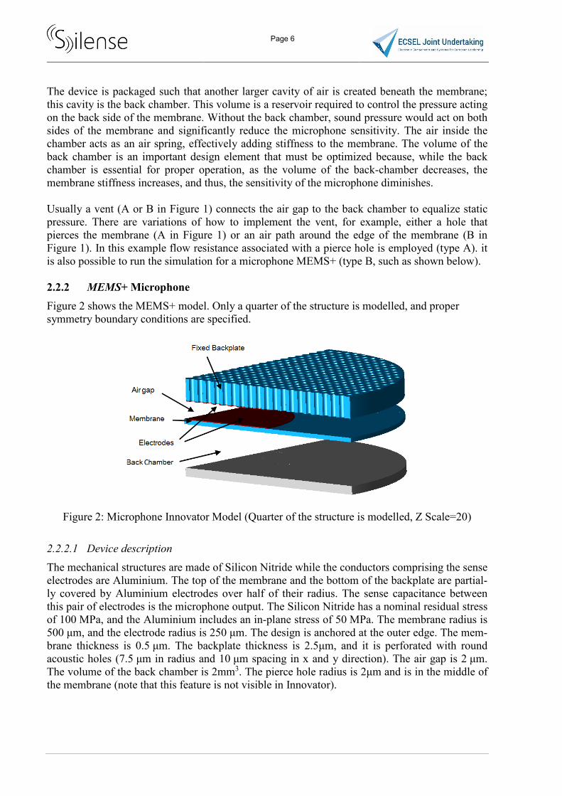
The device is packaged such that another larger cavity of air is created beneath the membrane; this cavity is the back chamber. This volume is a reservoir required to control the pressure acting on the back side of the membrane. Without the back chamber, sound pressure would act on both sides of the membrane and significantly reduce the microphone sensitivity. The air inside the chamber acts as an air spring, effectively adding stiffness to the membrane. The volume of the back chamber is an important design element that must be optimized because, while the back chamber is essential for proper operation, as the volume of the back-chamber decreases, the membrane stiffness increases, and thus, the sensitivity of the microphone diminishes. Usually a vent (A or B in Figure 1) connects the air gap to the back chamber to equalize static pressure. There are variations of how to implement the vent, for example, either a hole that pierces the membrane (A in Figure 1) or an air path around the edge of the membrane (B in Figure 1). In this example flow resistance associated with a pierce hole is employed (type A). it is also possible to run the simulation for a microphone MEMS+ (type B, such as shown below). 2.2.2 MEMS+ Microphone Figure 2 shows the MEMS+ model. Only a quarter of the structure is modelled, and proper symmetry boundary conditions are specified.
Figure 2: Microphone Innovator Model (Quarter of the structure is modelled, Z Scale=20)
2.2.2.1 Device description The mechanical structures are made of Silicon Nitride while the conductors comprising the sense electrodes are Aluminium. The top of the membrane and the bottom of the backplate are partial-ly covered by Aluminium electrodes over half of their radius. The sense capacitance between this pair of electrodes is the microphone output. The Silicon Nitride has a nominal residual stress of 100 MPa, and the Aluminium includes an in-plane stress of 50 MPa. The membrane radius is 500 μm, and the electrode radius is 250 μm. The design is anchored at the outer edge. The mem-brane thickness is 0.5 μm. The backplate thickness is 2.5μm, and it is perforated with round acoustic holes (7.5 μm in radius and 10 μm spacing in x and y direction). The air gap is 2 μm. The volume of the back chamber is 2mm3. The pierce hole radius is 2μm and is in the middle of the membrane (note that this feature is not visible in Innovator).

Page 7
2.2.2.2 Vent Leakage Resistance (A) The leakage flow resistance through the vent must be obtained from either an analytical model, empirical data, or another simulation outside of MEMS+. For this tutorial we use the analytical model described below. The leakage Ra flow resistance value is described by the following equation: Equation 1:
where l is the thickness of the membrane, r is the hole radius, μ is the viscosity of air (μ = 1.71×10¬5Pa•s at 273.15K).
The leakage flow resistance of the vent of this design is calculated as Ra = 1.36×10¹²kg•s 1•m-4. Note that this leakage flow resistance value is appropriate for the complete device; however, be-cause we are only modelling a quarter of the model, we will need to adjust the value, as calcula-ted in section 2.4.4. 2.2.2.3 Effective Compliance Another important characteristic of a microphone is the effective compliance, Ca, of the back chamber, which is required to calculate the roll-off frequency (see section 2.4.3). It can be calcu-lated using the equation [2]: Equation 2:
where ρair is the density of air, c the speed of sound, and β the compressibility of air (β = 7.05×10⁶Pa-1 at 273.15K).
MEMS+ accepts both the compressibility and density of fluids in the material database. The chamber volume, Vch, is determined by the process description and the planar area of the mem-brane. However, the Fluid Back Chamber component also includes a Chamber Volume Scale Factor parameter that allows users to scale the size of their fluid cavity without needing to arbi-trarily modify their process description. The Chamber Volume Scale Factor will be explained in more detail in the section beginning on page T3-28. The acoustic compliance of this microphone is thus
Ca = 2mm3•7.05×10 6Pa 1 = 1.41×10 14m4•s2•kg In the next section the creation of the model is described. The construction of the model is shown step by step, starting with the membrane to which other components are added to comple-te the design.

Page 8
3 MODEL CREATION 3.1 Material Database Add variables and update materials properties
1. Navigate to Material Database module. See the available materials. 2. See the variable pane, exercise the Right Click Button (RMB) inside this panel and create
a group called Stress that contains two variables called Silicon Nitride and Aluminium. Expose those variables (RMB > Expose).
3. Change the pre-stress in-plane isotropic stress value of Aluminium and Silicon Nitride with the corresponding previously created variable. Pay attention to the unit (MPa).
Figure 3: Material Database plugin
3.2 Process Editor You will encounter an update bar on top of a module every time its dependent module has been updated. Clicking this bar will update the module with the changes of the dependent module. Please click this bar each time you need. Complete the Process
1. Navigate to Process Editor module. Compare to Figure 4 (two steps are missing: MechanicalMaterial2 and BackPlateCut).
2. Add a Stack Material step (RMB the substrate and select add). Configure this step properties; Layer Name: Backplate, Material: Silicon Nitride, Thickness: 2.5um.
3. Add a Straight Cut step set its Mask Name to BackplateCut. 4. Set its mask to BackplateMask. 5. Drag and drop the steps to their correct position (See Figure 4, next page).

Page 9
Figure 4: Process pane as seen in the Process Editor Plugin
Figure 5: Layer Table pane
3.3 Component Library The mechanical membrane of the device we are designing is constituted of 6 individual compo-nents made of three types (1 Pie, 2 ArcElectrode and 4 ArcOurter). The Component types are defined in the component library and have their settings and addable child tuned to ease and accelerate the device creation made in Innovator.
Figure 6: The Membrane (Component view on the right and Mechanical vies on the left)
Explore the Component Library (see pictures next page) 1. First navigate to Innovator, RMB component tree and select Add. This the complete list
of components you can use to create the 3D design. 2. Navigate to Component Library module, now see the User Library available Prototypes
list: the list of Innovator addable component is defined here. Compare to Figure 6 ArcOuter component and its sub-components are missing
3. Add Backplate to the layers of Inherited Gap child components of Pie and Arc Electrode components.
4. Copy and paste (RMB or CTRL-C/V) ArcElectrode component and remane it ArcOuter. 5. Change the layer property of ArcOuter and its child Inherited Gap to respectively
Membrane only and Bacplate only. 6. Change ArcOuter
o Outer Radius Face Type to Fix o Gap Model to Squeezed Film only

Page 10
Figure 7: Component Library
Page 11
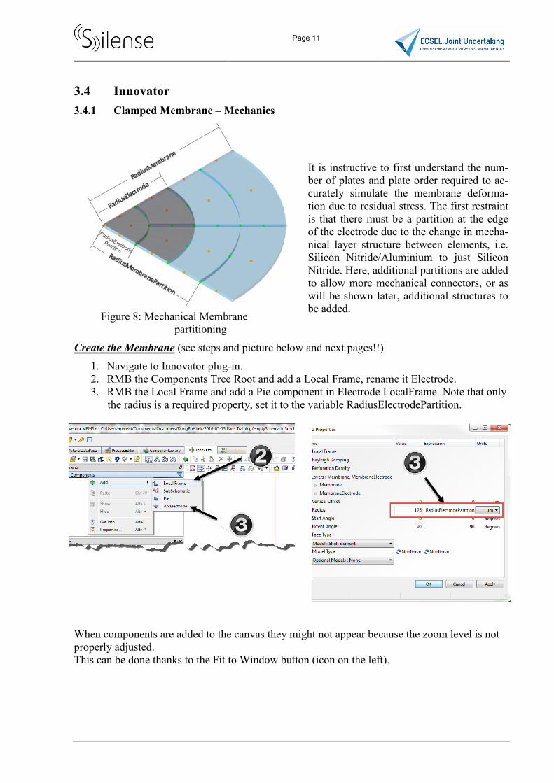
3.4 Innovator 3.4.1 Clamped Membrane – Mechanics
Figure 8: Mechanical Membrane
partitioning
It is instructive to first understand the num-ber of plates and plate order required to ac-curately simulate the membrane deforma-tion due to residual stress. The first restraint is that there must be a partition at the edge of the electrode due to the change in mecha-nical layer structure between elements, i.e. Silicon Nitride/Aluminium to just Silicon Nitride. Here, additional partitions are added to allow more mechanical connectors, or as will be shown later, additional structures to be added.
Create the Membrane (see steps and picture below and next pages!!) 1. Navigate to Innovator plug-in. 2. RMB the Components Tree Root and add a Local Frame, rename it Electrode. 3. RMB the Local Frame and add a Pie component in Electrode LocalFrame. Note that only
the radius is a required property, set it to the variable RadiusElectrodePartition.
When components are added to the canvas they might not appear because the zoom level is not properly adjusted. This can be done thanks to the Fit to Window button (icon on the left).

Page 12
4. RMB > Add two ArcElectrode components to Electrode Local Frame with properties set as shown in the picture below.
5. RMB the Component Tree Root and add another Local Frame at the tree root level and rename it OuterRing.
6. Add four ArcOuter components with properties set as shown in the picture below.
Page 13
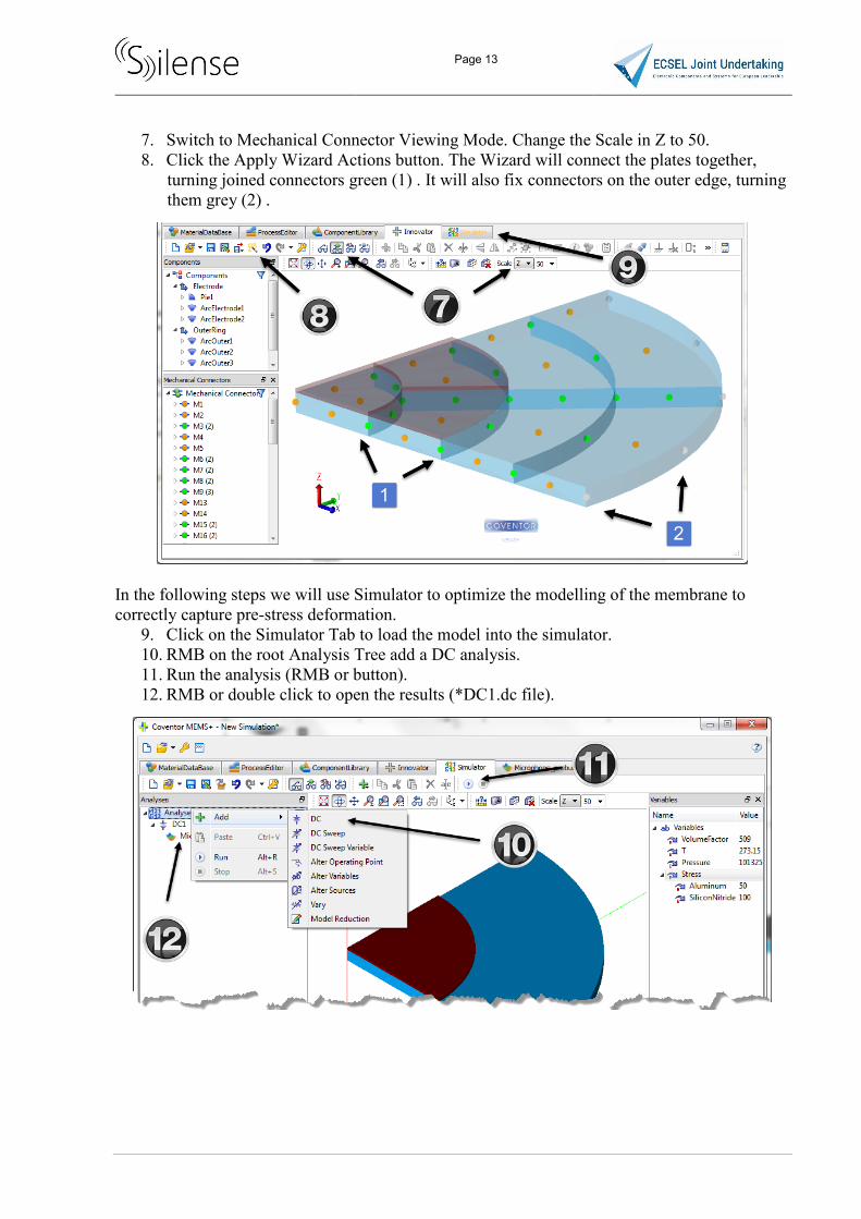
7. Switch to Mechanical Connector Viewing Mode. Change the Scale in Z to 50. 8. Click the Apply Wizard Actions button. The Wizard will connect the plates together,
turning joined connectors green (1) . It will also fix connectors on the outer edge, turning them grey (2) .
In the following steps we will use Simulator to optimize the modelling of the membrane to correctly capture pre-stress deformation.
9. Click on the Simulator Tab to load the model into the simulator. 10. RMB on the root Analysis Tree add a DC analysis. 11. Run the analysis (RMB or button). 12. RMB or double click to open the results (*DC1.dc file).
Page 14
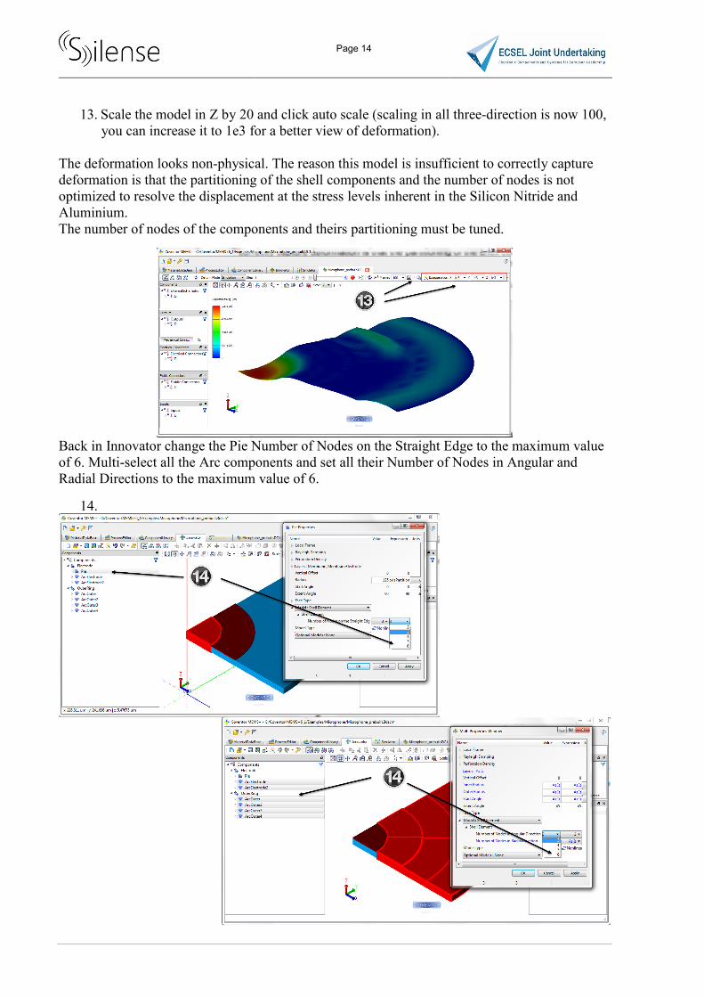
13. Scale the model in Z by 20 and click auto scale (scaling in all three-direction is now 100, you can increase it to 1e3 for a better view of deformation).
The deformation looks non-physical. The reason this model is insufficient to correctly capture deformation is that the partitioning of the shell components and the number of nodes is not optimized to resolve the displacement at the stress levels inherent in the Silicon Nitride and Aluminium. The number of nodes of the components and theirs partitioning must be tuned.
Back in Innovator change the Pie Number of Nodes on the Straight Edge to the maximum value of 6. Multi-select all the Arc components and set all their Number of Nodes in Angular and Radial Directions to the maximum value of 6.
14.
Page 15
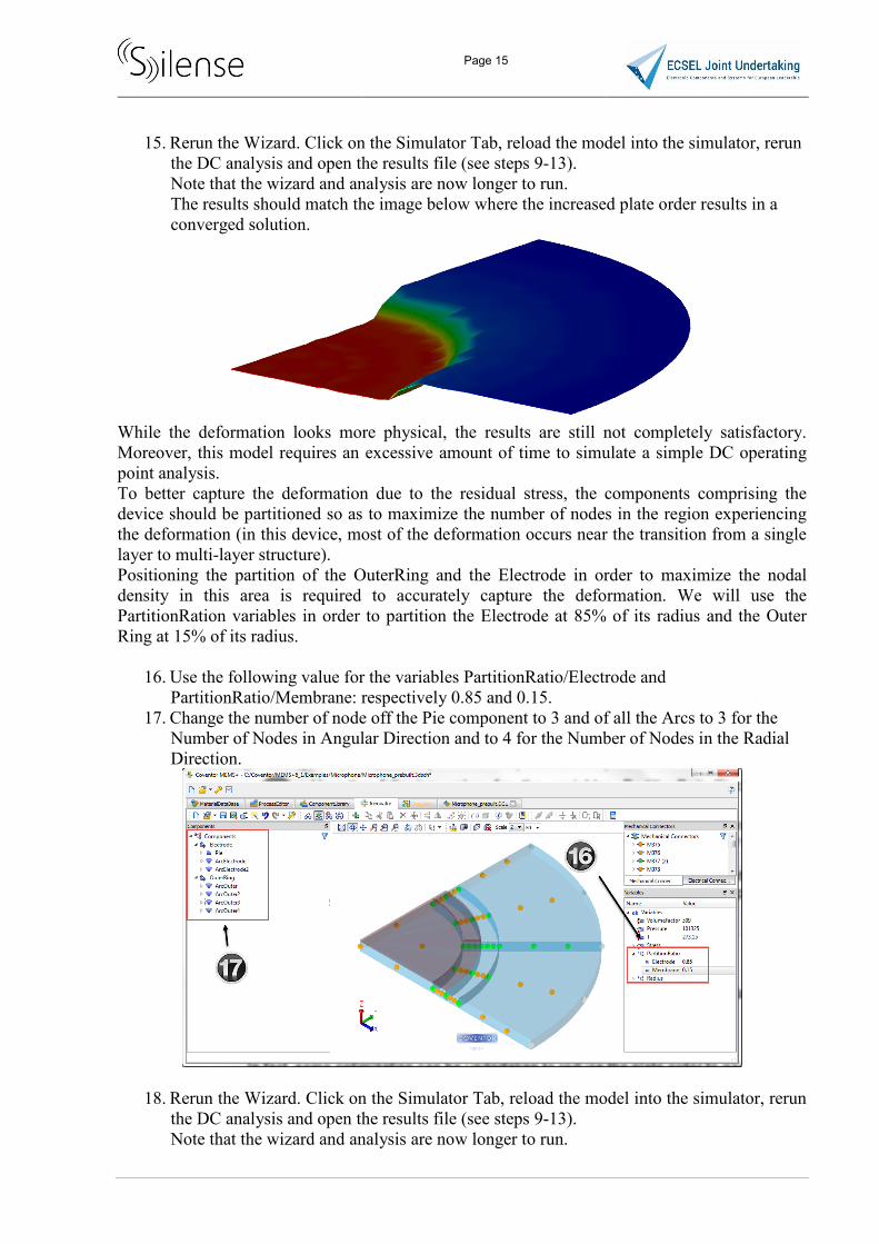
15. Rerun the Wizard. Click on the Simulator Tab, reload the model into the simulator, rerun the DC analysis and open the results file (see steps 9-13). Note that the wizard and analysis are now longer to run. The results should match the image below where the increased plate order results in a converged solution.
While the deformation looks more physical, the results are still not completely satisfactory. Moreover, this model requires an excessive amount of time to simulate a simple DC operating point analysis. To better capture the deformation due to the residual stress, the components comprising the device should be partitioned so as to maximize the number of nodes in the region experiencing the deformation (in this device, most of the deformation occurs near the transition from a single layer to multi-layer structure). Positioning the partition of the OuterRing and the Electrode in order to maximize the nodal density in this area is required to accurately capture the deformation. We will use the PartitionRation variables in order to partition the Electrode at 85% of its radius and the Outer Ring at 15% of its radius.
16. Use the following value for the variables PartitionRatio/Electrode and PartitionRatio/Membrane: respectively 0.85 and 0.15.
17. Change the number of node off the Pie component to 3 and of all the Arcs to 3 for the Number of Nodes in Angular Direction and to 4 for the Number of Nodes in the Radial Direction.
18. Rerun the Wizard. Click on the Simulator Tab, reload the model into the simulator, rerun the DC analysis and open the results file (see steps 9-13). Note that the wizard and analysis are now longer to run.
Page 16
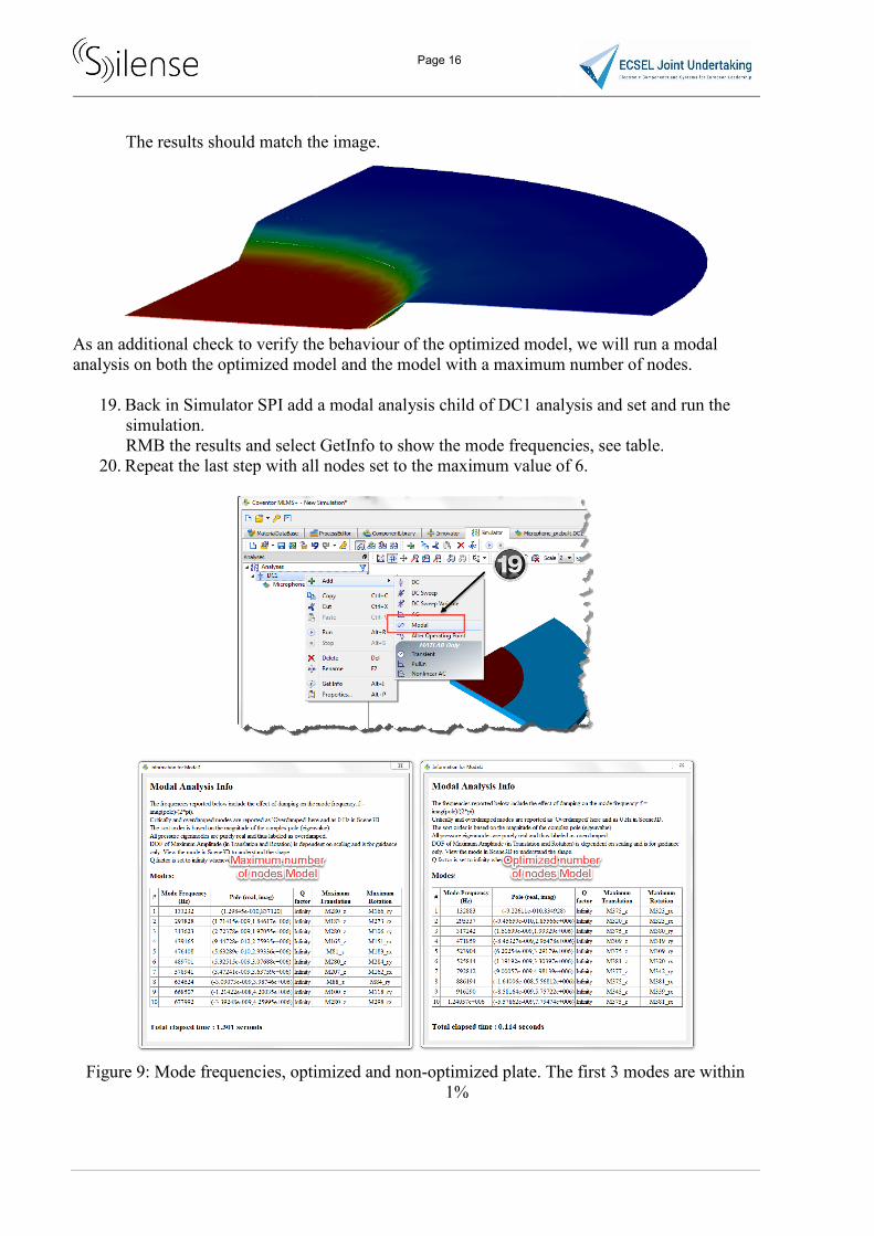
The results should match the image.
As an additional check to verify the behaviour of the optimized model, we will run a modal analysis on both the optimized model and the model with a maximum number of nodes.
19. Back in Simulator SPI add a modal analysis child of DC1 analysis and set and run the simulation. RMB the results and select GetInfo to show the mode frequencies, see table.
20. Repeat the last step with all nodes set to the maximum value of 6.
Figure 9: Mode frequencies, optimized and non-optimized plate. The first 3 modes are within
1%

Page 17
3.4.2 Microphone Backplate Since MEMS+6.1, it is possible to create flexible backplate thanks to the new component Mova-ble Gap. This is based on microphone modelled with a rigid backplate nevertheless the steps to create a flexible backplate are also presented below. Having determined the layout and elements to model the mechanics of the membrane, the remainder of the microphone can be created. The Backplate consists of an electrical and a fluidic model. You can define both of these models with the Gap component, which can include an Electrode/Contact model, a Squeezed Film Damping model, or both. Create the Backplate
1. Back in Innovator RMB the Pie component and Add an Inherited Gap. 2. RMB the Inherited Gap and add a Pressure load. 3. Repeat step one and two for the 6 Arc components. To add an Inherited Gap and a
Pressure load on this inherited gap on each Arc components.
4. Switch to Electrical Connectors Viewing Mode. Note that the Inherited Gaps of the Pie and the two Arc Electrode components contains an Electrode model (see their properties). Note that therefore, there are 3 pairs of Electrical Connectors in the Electrical Connectors tree (1).
5. Click the Apply Wizard Actions button. The Wizard will connect touching Electrical Connectors together ( (1) =>(2) ). There is now two remaining Electrical Connectors, on for the Electrode attached to the Membrane and one for the Backplate.

Page 18
The wizard fails and throws an error message. No Fluidic Connectors are Exposed, no boundary condition can be applied to fluidic, the model is not properly constrained. As if air is trapped inside the device and cannot escape at all (nothing would move). At least one Fluidic Connectors must be Exposed, at step 9 the Microphone Input Pressure (on top of the Backplate is exposed).
6. Click on Electrical Connector and see on the canvas (still in Electrical Viewing Mode) which one is the attached to the Backplate or the Membrane. RMB and rename them respectively Membrane and Backplate. Expose the two Electrical Connectors.
7. In the Outputs pane, rename Cap1 to OutputCap, and expose it. 8. Switch to Fluidic Connectors Viewing Mode. Rename the fluidic connector group that
represents the top of the Backplate the fluid connectors InputPressure and expose it. See picture below. Click the Apply Wizard Actions button, no error message shows up this time.
Page 19
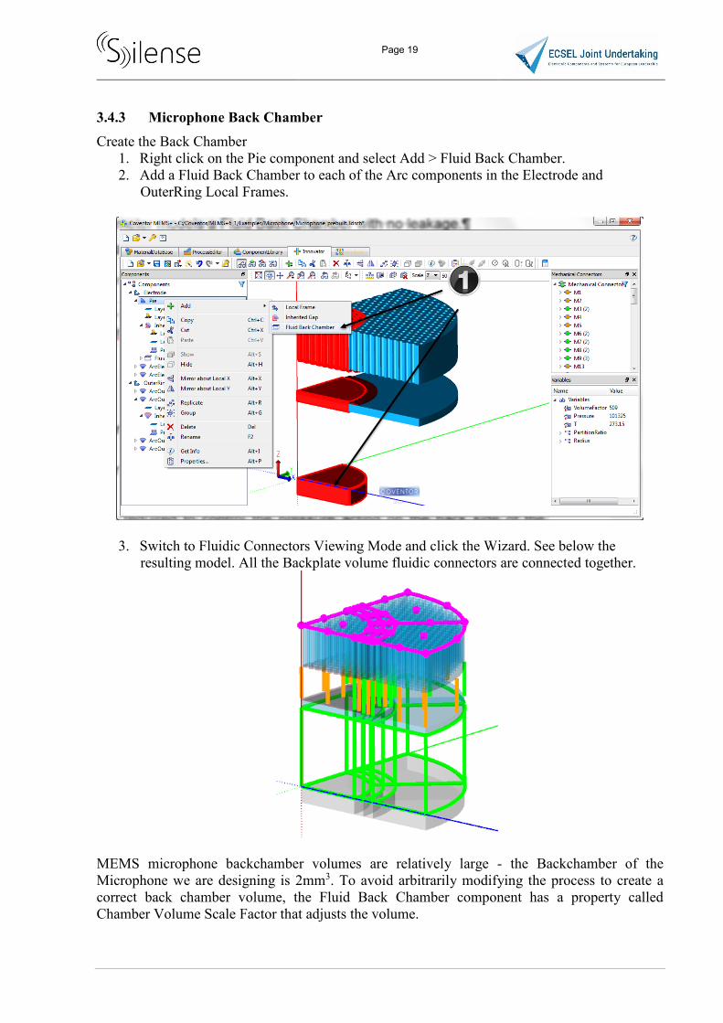
3.4.3 Microphone Back Chamber Create the Back Chamber
1. Right click on the Pie component and select Add > Fluid Back Chamber. 2. Add a Fluid Back Chamber to each of the Arc components in the Electrode and
OuterRing Local Frames.
3. Switch to Fluidic Connectors Viewing Mode and click the Wizard. See below the resulting model. All the Backplate volume fluidic connectors are connected together.
MEMS microphone backchamber volumes are relatively large - the Backchamber of the Microphone we are designing is 2mm3. To avoid arbitrarily modifying the process to create a correct back chamber volume, the Fluid Back Chamber component has a property called Chamber Volume Scale Factor that adjusts the volume.

Page 20
The effective volume is thus the volume encapsulated between the component layer and the Fluid Back Chamber Fixed Layer, as defined by the process and device area, multiplied by the Chamber Volume Scale Factor.
Figure 10: Pie FluidBackChamber GetInfo (left) and properties window (right)
4. Change the VolumeFactor Variable value from 1 to 509.
3.4.4 Microphone Vent (Pierce Hole) There are two design trends in MEMS microphones to create the vent between the membrane air gap (front side) and back chamber (back side) that allows for equalizing static pressure. Air can either flow through a pierce hole on the membrane or through a channel around the membrane edge. The microphone used in this tutorial is modelled with a pierce hole (Pierce Hole: A in Figure 1). The Pierce Hole radius is 2μm, and it introduces a leakage between the air gap (above the membrane) and the back chamber (below the membrane). The total leakage flow resistance due to this hole, originally calculated with the equation in Leakage Resistance RFullDevice = 1.36×10¹²kg•s-1•m4, applies to the complete model. Because we are modelling only a quarter of the complete device (and because the four quarter models would be configured in a parallel configuration) the leakage flow resistance RQuarterModel of quarter model of the device is 4 time the full one. Equation 3:
RQuarterModel = 4×RFullDevice = 5.44×10¹²kg•s 1•m 4. This leakage is modelled with a lump component: Fluid Resistance.

Page 21
Implement the Vent flow through pierce hole 1. Right click the Component Tree root and select Add > Fluid Resistance.
2. Set Pin1 Location to (0, 0, 5um) and Pin2 Location to (0, 0, 5.6um), this are respectively
on bottom and top of the Membrane on the center. Set the Resistance value to Resistance to 5.44×10¹²kg•s-1•m 4
3. In the Fluidic Connectors Viewing Mode see the tow newly created Fluidic Connector. And rename them VentPierceHoleBottom and VentPierceHoleTop.
4. Click the Wizard. Note that the top and bottom new connectors are now respectively connected to a Squeezed Film Damping fluidic connector and the Back-Chamber Fluid Connectors. The result is shown on the figure below.
Page 22
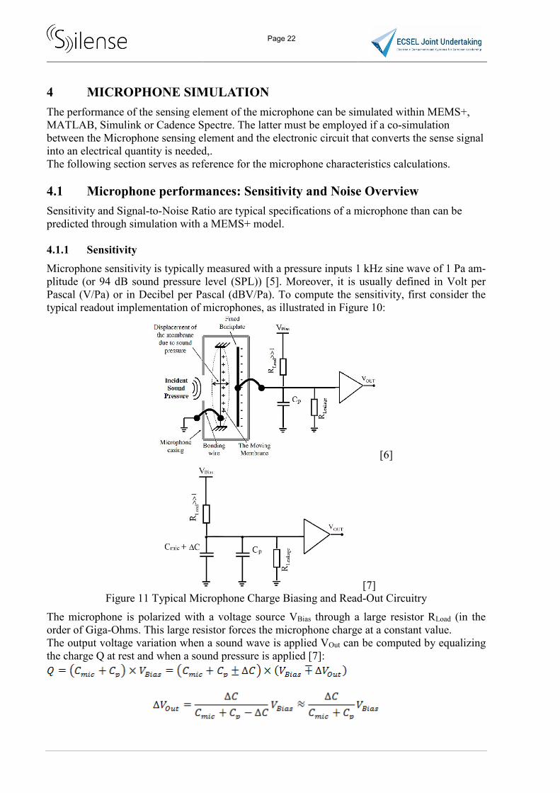
4 MICROPHONE SIMULATION The performance of the sensing element of the microphone can be simulated within MEMS+, MATLAB, Simulink or Cadence Spectre. The latter must be employed if a co-simulation between the Microphone sensing element and the electronic circuit that converts the sense signal into an electrical quantity is needed,. The following section serves as reference for the microphone characteristics calculations. 4.1 Microphone performances: Sensitivity and Noise Overview Sensitivity and Signal-to-Noise Ratio are typical specifications of a microphone than can be predicted through simulation with a MEMS+ model. 4.1.1 Sensitivity Microphone sensitivity is typically measured with a pressure inputs 1 kHz sine wave of 1 Pa am-plitude (or 94 dB sound pressure level (SPL)) [5]. Moreover, it is usually defined in Volt per Pascal (V/Pa) or in Decibel per Pascal (dBV/Pa). To compute the sensitivity, first consider the typical readout implementation of microphones, as illustrated in Figure 10:
[6]
[7] Figure 11 Typical Microphone Charge Biasing and Read-Out Circuitry
The microphone is polarized with a voltage source VBias through a large resistor RLoad (in the order of Giga-Ohms. This large resistor forces the microphone charge at a constant value. The output voltage variation when a sound wave is applied VOut can be computed by equalizing the charge Q at rest and when a sound pressure is applied [7]:
Page 23
It follows the definition of the voltage sensitivity (at 1 kHz) [5]: Equation 4:
Where VBias is the bias voltage applied to the membrane, ΔC is the capacitance change due to a 1 Pa magnitude input pressure (F/Pa), and Ctotal is the sum of the microphone static capacitance and the parasitic capacitance between the backplate and the ground. The sensitivity in decibel is defined as [5]: Equation 5:
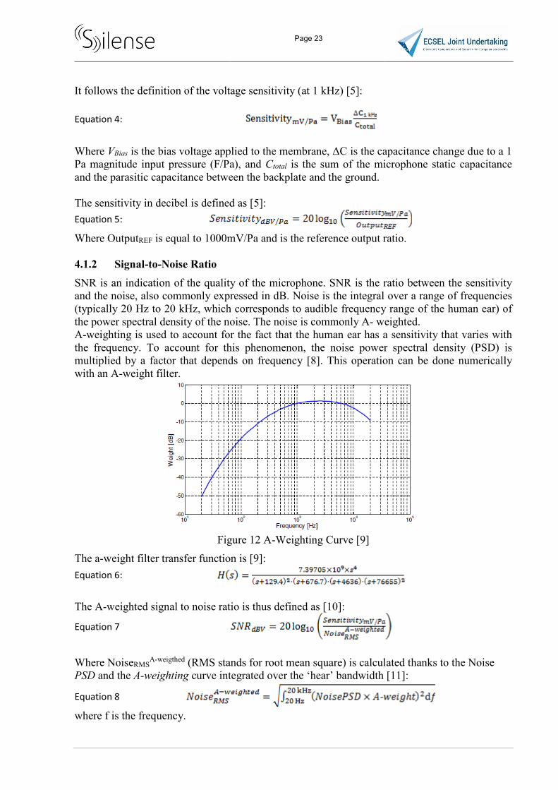
Where OutputREF is equal to 1000mV/Pa and is the reference output ratio. 4.1.2 Signal-to-Noise Ratio SNR is an indication of the quality of the microphone. SNR is the ratio between the sensitivity and the noise, also commonly expressed in dB. Noise is the integral over a range of frequencies (typically 20 Hz to 20 kHz, which corresponds to audible frequency range of the human ear) of the power spectral density of the noise. The noise is commonly A- weighted. A-weighting is used to account for the fact that the human ear has a sensitivity that varies with the frequency. To account for this phenomenon, the noise power spectral density (PSD) is multiplied by a factor that depends on frequency [8]. This operation can be done numerically with an A-weight filter.
Figure 12 A-Weighting Curve [9]
The a-weight filter transfer function is [9]: Equation 6:
The A-weighted signal to noise ratio is thus defined as [10]:
Equation 7
Where NoiseRMS
A-weigthed (RMS stands for root mean square) is calculated thanks to the Noise PSD and the A-weighting curve integrated over the ‘hear’ bandwidth [11]:
Equation 8
where f is the frequency.
Page 24
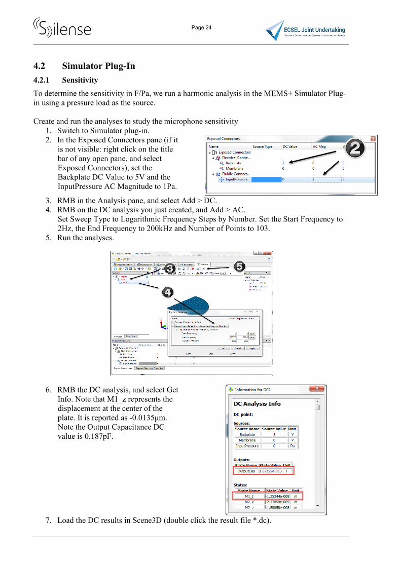
4.2 Simulator Plug-In 4.2.1 Sensitivity To determine the sensitivity in F/Pa, we run a harmonic analysis in the MEMS+ Simulator Plug-in using a pressure load as the source. Create and run the analyses to study the microphone sensitivity
1. Switch to Simulator plug-in. 2. In the Exposed Connectors pane (if it
is not visible: right click on the title bar of any open pane, and select Exposed Connectors), set the Backplate DC Value to 5V and the InputPressure AC Magnitude to 1Pa.
3. RMB in the Analysis pane, and select Add > DC. 4. RMB on the DC analysis you just created, and Add > AC.
Set Sweep Type to Logarithmic Frequency Steps by Number. Set the Start Frequency to 2Hz, the End Frequency to 200kHz and Number of Points to 103.
5. Run the analyses.
6. RMB the DC analysis, and select Get Info. Note that M1_z represents the displacement at the center of the plate. It is reported as -0.0135μm. Note the Output Capacitance DC value is 0.187pF.
7. Load the DC results in Scene3D (double click the result file *.dc).

Page 25
8. Set the Z scale to 10 and click on the Set Exaggeration Automatically icon. The results are in Figure 13.
Figure 13 3D deformation result of a 5V bias DC in Scene3D
9. Load the AC results in Scen3D (back in Innovator plug-in double click the result file *.ac).
10. Set the Z scale to 10. Move the sliding bar at approximately its center. Click on the Set Exaggeration Automatically icon. Move back the slider to the beginning and play the animation.
11. In Scene3D, click on the Open New Graph icon. 12. Expand the Outputs tree until the OutputCap(Membrane, Backplate) entry is shown.
Drag and drop the OutputCap to 2D plot window. 13. Double click on the X axis to open the properties dialog. Expand the X Axis list, and
change the Scale to Log. Click on OK to apply. The results are in Figure 14 below.
Figure 14: AC results in Scene3D

Page 26
Roll-off frequency: The low frequency roll-off shown in Figure 13 is the result of the vent resistance and the back-chamber compliance. The roll-off frequency of the microphone can be obtained with the following equation: Equation 9:
where Ra is the leakage flow resistance, and Ca the acoustic compliance of the microphone. Here Ra=1.36×10¹²kg/s/m4, Ca =1.42×10¹⁴m4s2/kg (see section 1.2.2), fRO = 8.24Hz. Microphone sensitivity The sensitivity of the microphone (in mV/Pa) can be computed with Equation 4 and Equation 5 introduced in section 3.1.1, with VBias = 5 V, capacitance sensitivity measured at 1 kHz is ΔC1 kHz=85.4aF/Pa and static capacitance of the microphone is Ctotal = 187.2 fF (parasitic capacitances are ignored). Because only a quarter of the microphone the capacitances must be multiplied by four:
The sensitivity can be expressed in decibel:
4.2.2 Pull-In Analysis The Pull-in analysis is used to compute system instabilities; it can be used to compute pull-in voltages, as well as lift-off voltages and the behavior of the device between and beyond those voltages. Pull-in analysis should be run if the DC Sweep exhibits a discontinuity or fails to converge; it avoids the challenges of a DC sweep by using an independent variable, assigned the name of lambda, to follow the curve of the many workable solutions to force balance rather than compute one of the solutions to force balance at a given voltage. In operation, a condenser microphone is often polarized with a voltage applied in between the membrane and the backplate. To set this voltage, one must take precaution to not exceed the pull-in voltage which will put in contact and stuck the two electrodes. Create and run a DC-Sweep and a Pull-in analyses.
1. RMB on the Analyses pane and select Add > AC with the following settings: Sweep Source: Backplate, Backplate: Linear by Increment, Start Value: 0, End Value: 30 and Increment: 1.
2. Rune the analysis.
This analysis fails at ~25 V this is certainly because the voltage sweep is reaching an instability that the DC solver cannot solve.

Page 27
We will use the advanced pull-in analysis to simulates beyond this voltage value.
3. Open the Scene3D results and plot the displacing of the Mechanical connectors M1 4. The Membrane is moving toward the Backplate. The simulation stops at 25V and dz =
0.57μm.
5. RMB on the Analyses pane and select Add > PullIn with the settings on the following screenshot:

Page 28
6. Open the results in Scene3D. Plot the mechanical connectors M1.
The pullin analysis result shows the many instabilities though the complete curve of equilibrium. Here the pullin (colpase) value is 25.88V (see getInfo). 4.2.3 Noise Spectral Density Starting with version 6.3 MEMS+ offers the possibility to run Noise analysis within the Simula-tor plug-in. This analysis computes the spectral density of noise of every states and inputs of the model (e.g. capacitance outputs in F/√Hz, mechanical connectors displacement in m/√Hz). Noise sources are Squeezed-Film Damping elements, Lumped Fluid Resistances. Create and run the analyses to study the microphone noise
1. In the Analyses tree, RMB DC1 and select Add > Noise Set Sweep Type to Logarithmic Frequency Steps by Number. Set the Start Frequency to 2Hz, the End Frequency to 200kHz and Number of Points to 103.
2. Load the Noise result file in Scene3D (double click the result file *.dc). Open a new graph window and plot the OutputCapat (set the scale to log/log)

Page 29
With this capacitance spectral density of noise, it is possible to compute the Signal-to-Noise Ratio of the modeled microphone. This would require some additional postprocessing that can be done for example in excel spreadsheet. Nevertheless, Signal-to-Noise Ratio computed thanks to this curve are demonstrated in the following MATLAB and Cadence sections. 4.3 MATLAB Scripting MEMS+ MATLAB scripting interface allows model import, manipulation and simulation directly from the MATLAB command line interface. Available DC, DC sweep, modal, AC, Transient, Pull-In, Nonlinear AC multiple-variable parametric simulations can be run without requiring any additional toolbox. The scripting code follows the same structural hierarchy as the MEMS+ graphic interface:
Figure 15: MATLAB interface
4.3.1 Configure MATLAB/MEMS+ 1. Start MATLAB 2. Configure MEMS+ for MATLAB environment:
Execute (e.g. drag and drop in the command window) the script: configureMatlabForMEMSplus.m located at: C:\Coventor\MEMS+6\runtime\matlab.
3. Set your working directory to the folder containing the MEMS+ files previously created. In this section, we recommend typing the line of code in the MATLAB Editor and to save the script file (*.m) regularly. The script can then be rune (MATLAB shortcut F5) or individual highlighted lines can be evaluated (F9). 4.3.2 Sensitivity Run analyses in MATLAB to study the microphone sensitivity
1. Create a Simulator MATLAB document from the Microphone 3D schematic file (.3dsch): h = cov.memsplus.Simulation(‘SchematicName.3dsch’);
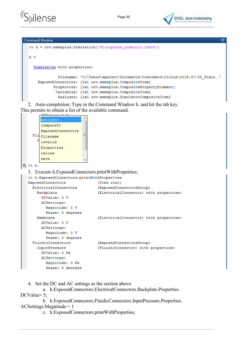
Page 30
2. Auto-completion: Type in the Command Window h. and hit the tab key.
This permits to obtain a list of the available command.
3. Execute h.ExposedConnectors.printWithProperties;
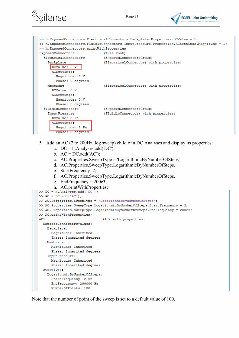
4. Set the DC and AC settings as the section above: a. h.ExposedConnectors.ElectricalConnectors.Backplate.Properties.
DCValue= 5; b. h.ExposedConnectors.FluidicConnectors.InputPressure.Properties.
ACSettings.Magnitude = 1 c. h.ExposedConnectors.printWithProperties;
Page 31
5. Add an AC (2 to 200Hz, log sweep) child of a DC Analyses and display its properties: a. DC = h.Analyses.add('DC'); b. AC = DC.add('AC'); c. AC.Properties.SweepType = 'LogarithmicByNumberOfSteps'; d. AC.Properties.SweepType.LogarithmicByNumberOfSteps. e. StartFrequency=2; f. AC.Properties.SweepType.LogarithmicByNumberOfSteps. g. EndFrequency = 200e3; h. AC.printWithProperties;
Note that the number of point of the sweep is set to a default value of 100.
Page 32
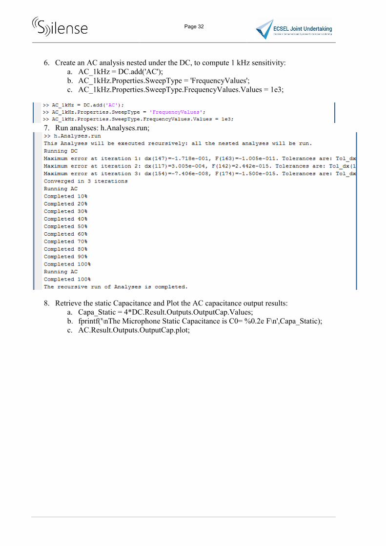
6. Create an AC analysis nested under the DC, to compute 1 kHz sensitivity: a. AC_1kHz = DC.add('AC'); b. AC_1kHz.Properties.SweepType = 'FrequencyValues'; c. AC_1kHz.Properties.SweepType.FrequencyValues.Values = 1e3;
7. Run analyses: h.Analyses.run;
8. Retrieve the static Capacitance and Plot the AC capacitance output results: a. Capa_Static = 4*DC.Result.Outputs.OutputCap.Values; b. fprintf('\nThe Microphone Static Capacitance is C0= %0.2e F\n',Capa_Static); c. AC.Result.Outputs.OutputCap.plot;

Page 33
Figure 16 AC results in MATLAB
9. Compute the Sensitivity (with Equation 4 and Equation 5):
a. CapaSensitivity = 4*abs(AC_1kHz.Result.Outputs.OutputCap.Values(:,2)); b. Sensitivity_mV = 5*CapaSensitivity/(4*Capa_Static)*1000; c. Sensititvity_dBV = 20*log10(Sensitivity_mV/1000); d. fprintf('The Capacitance Sensitivity is Sensitivity_Capacitance= %.2s
F/Pa\n',CapaSensitivity); e. fprintf('The Voltage Sensitivity is Sensitivity_mVolt= %0.2f
mV/Pa\n',Sensitivity_mV); f. fprintf('The dB20 Voltage Sensitivity is Sensitivity_dBV= %0.2f
dB/Pa\n',Sensititvity_dBV);
Page 34
4.3.3 Signal-to-Noise Ratio Run analyses in MATLAB to study the microphone SNR
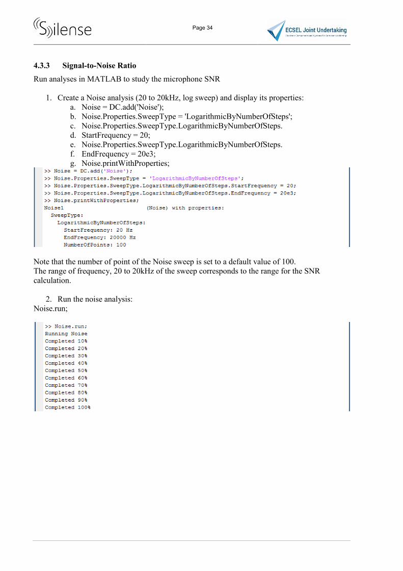
1. Create a Noise analysis (20 to 20kHz, log sweep) and display its properties: a. Noise = DC.add('Noise'); b. Noise.Properties.SweepType = 'LogarithmicByNumberOfSteps'; c. Noise.Properties.SweepType.LogarithmicByNumberOfSteps. d. StartFrequency = 20; e. Noise.Properties.SweepType.LogarithmicByNumberOfSteps. f. EndFrequency = 20e3; g. Noise.printWithProperties;
Note that the number of point of the Noise sweep is set to a default value of 100. The range of frequency, 20 to 20kHz of the sweep corresponds to the range for the SNR calculation.
2. Run the noise analysis: Noise.run;
Page 35
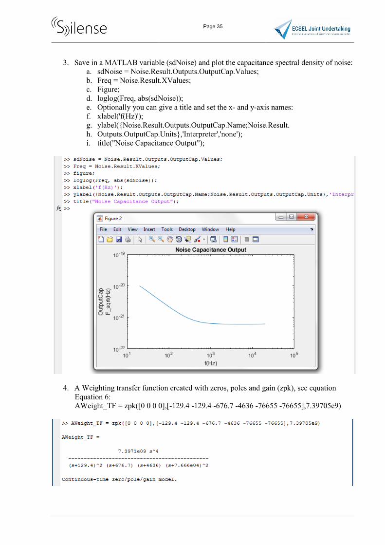
3. Save in a MATLAB variable (sdNoise) and plot the capacitance spectral density of noise: a. sdNoise = Noise.Result.Outputs.OutputCap.Values; b. Freq = Noise.Result.XValues; c. Figure; d. loglog(Freq, abs(sdNoise)); e. Optionally you can give a title and set the x- and y-axis names: f. xlabel('f(Hz)'); g. ylabel({Noise.Result.Outputs.OutputCap.Name;Noise.Result. h. Outputs.OutputCap.Units},'Interpreter','none'); i. title("Noise Capacitance Output");
4. A Weighting transfer function created with zeros, poles and gain (zpk), see equation Equation 6: AWeight_TF = zpk([0 0 0 0],[-129.4 -129.4 -676.7 -4636 -76655 -76655],7.39705e9)
Page 36
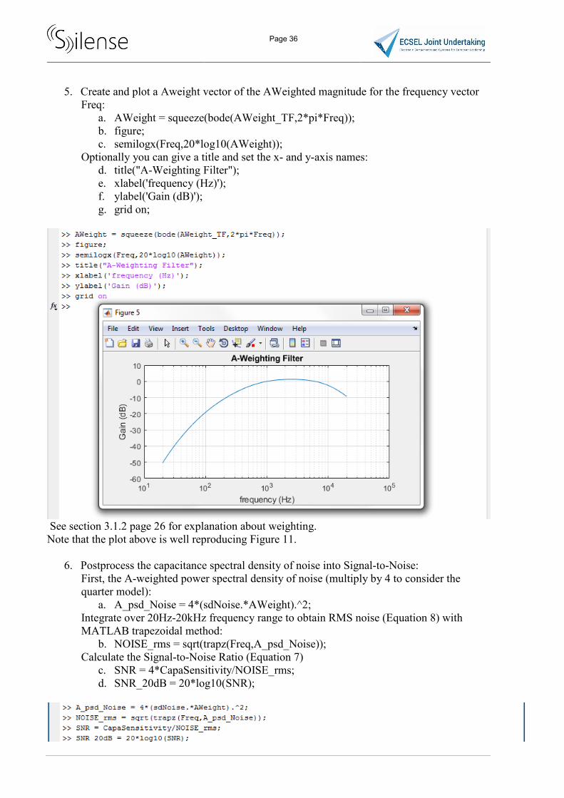
5. Create and plot a Aweight vector of the AWeighted magnitude for the frequency vector Freq:
a. AWeight = squeeze(bode(AWeight_TF,2*pi*Freq)); b. figure; c. semilogx(Freq,20*log10(AWeight));
Optionally you can give a title and set the x- and y-axis names: d. title("A-Weighting Filter"); e. xlabel('frequency (Hz)'); f. ylabel('Gain (dB)'); g. grid on;
See section 3.1.2 page 26 for explanation about weighting. Note that the plot above is well reproducing Figure 11.
6. Postprocess the capacitance spectral density of noise into Signal-to-Noise: First, the A-weighted power spectral density of noise (multiply by 4 to consider the quarter model):
a. A_psd_Noise = 4*(sdNoise.*AWeight).^2; Integrate over 20Hz-20kHz frequency range to obtain RMS noise (Equation 8) with MATLAB trapezoidal method:
b. NOISE_rms = sqrt(trapz(Freq,A_psd_Noise)); Calculate the Signal-to-Noise Ratio (Equation 7)
c. SNR = 4*CapaSensitivity/NOISE_rms; d. SNR_20dB = 20*log10(SNR);
Page 37
MATLAB trapezoidal numerical integration method:
7. Display results:
a. fprintf('\nThe 20-20kHz band RMS total noise is Noise_RMS= %0.3g F\n',NOISE_rms);
b. fprintf('The Signal-to-Noise Ratio is SNR= %0.3g 1/Pa\n',SNR); c. fprintf('The dB20 Signal-to-Noise Ratio is SNR_db20= %0.3g dB\n',SNR_20dB);
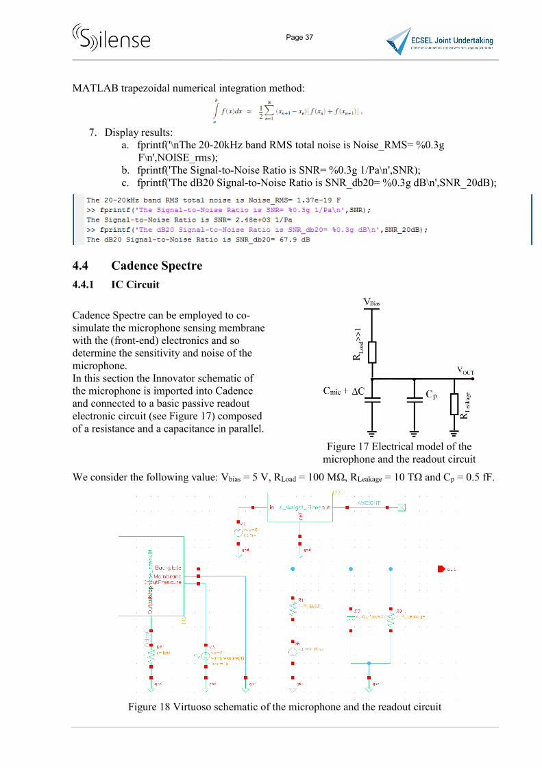
4.4 Cadence Spectre 4.4.1 IC Circuit Cadence Spectre can be employed to co-simulate the microphone sensing membrane with the (front-end) electronics and so determine the sensitivity and noise of the microphone. In this section the Innovator schematic of the microphone is imported into Cadence and connected to a basic passive readout electronic circuit (see Figure 17) composed of a resistance and a capacitance in parallel.
Figure 17 Electrical model of the
microphone and the readout circuit We consider the following value: Vbias = 5 V, RLoad = 100 MΩ, RLeakage = 10 TΩ and Cp = 0.5 fF.
Figure 18 Virtuoso schematic of the microphone and the readout circuit
Page 38
4.4.2 Create the Virtuoso 1. Start Cadence Virtuoso.
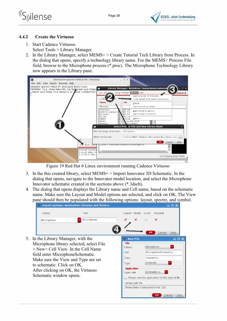
Select Tools > Library Manager. 2. In the Library Manager, select MEMS+ > Create Tutorial Tech Library from Process. In
the dialog that opens, specify a technology library name. For the MEMS+ Process File field, browse to the Microphone process (*.proc). The Microphone Technology Library now appears in the Library pane.
Figure 19 Red Hat 6 Linux environment running Cadence Virtuoso
3. In the this created library, select MEMS+ > Import Innovator 3D Schematic. In the dialog that opens, navigate to the Innovator model location, and select the Microphone Innovator schematic created in the sections above (*.3dsch).
4. The dialog that opens displays the Library name and Cell name, based on the schematic name. Make sure the Layout and Model options are selected, and click on OK. The View pane should then be populated with the following options: layout, spectre, and symbol.
5. In the Library Manager, with the
Microphone library selected, select File > New> Cell View. In the Cell Name field enter MicrophoneSchematic. Make sure the View and Type are set to schematic. Click on OK. After clicking on OK, the Virtuoso Schematic window opens.
Page 39
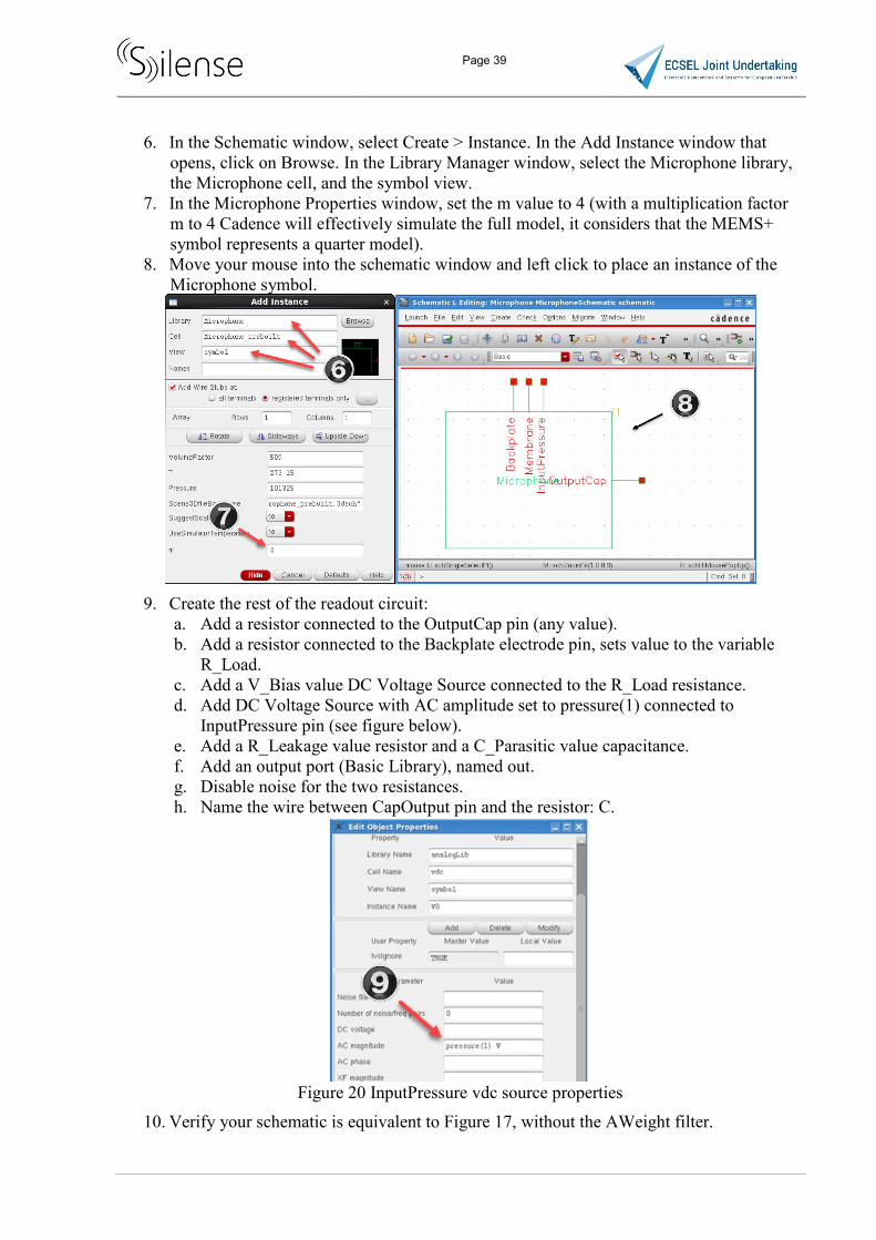
6. In the Schematic window, select Create > Instance. In the Add Instance window that opens, click on Browse. In the Library Manager window, select the Microphone library, the Microphone cell, and the symbol view.
7. In the Microphone Properties window, set the m value to 4 (with a multiplication factor m to 4 Cadence will effectively simulate the full model, it considers that the MEMS+ symbol represents a quarter model).
8. Move your mouse into the schematic window and left click to place an instance of the Microphone symbol.
9. Create the rest of the readout circuit:
a. Add a resistor connected to the OutputCap pin (any value). b. Add a resistor connected to the Backplate electrode pin, sets value to the variable
R_Load. c. Add a V_Bias value DC Voltage Source connected to the R_Load resistance. d. Add DC Voltage Source with AC amplitude set to pressure(1) connected to
InputPressure pin (see figure below). e. Add a R_Leakage value resistor and a C_Parasitic value capacitance. f. Add an output port (Basic Library), named out. g. Disable noise for the two resistances. h. Name the wire between CapOutput pin and the resistor: C.
Figure 20 InputPressure vdc source properties
10. Verify your schematic is equivalent to Figure 17, without the AWeight filter.
Page 40
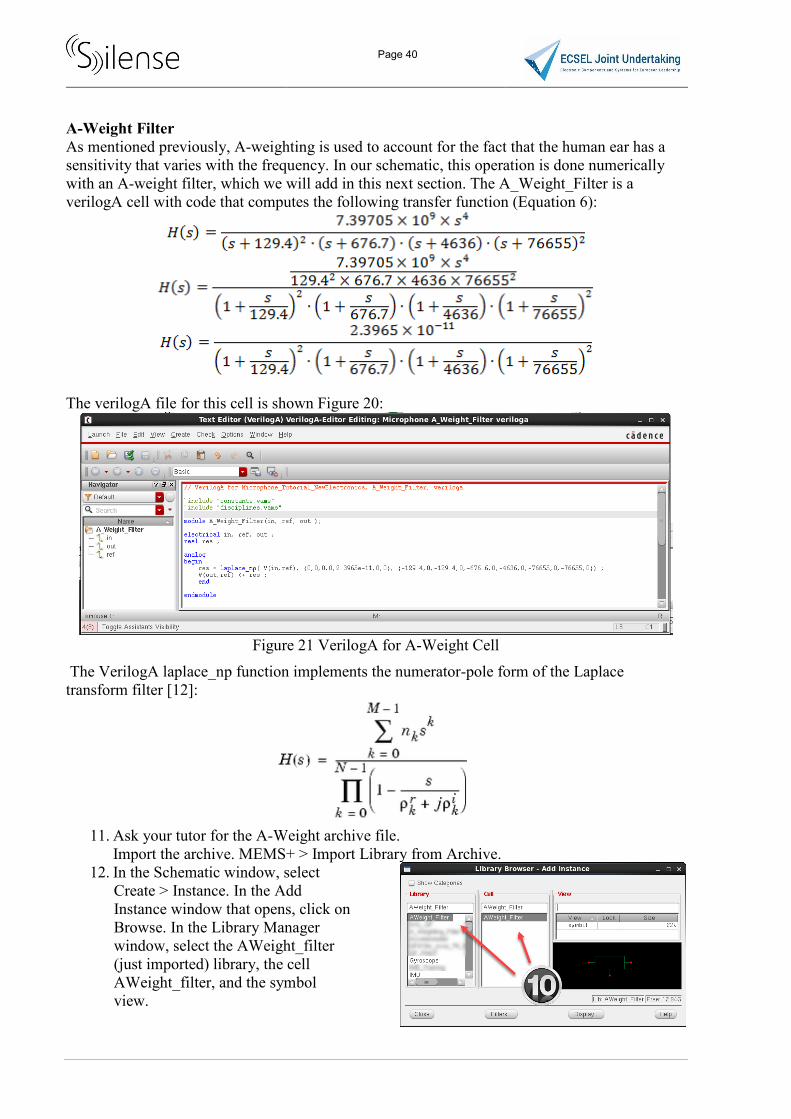
A-Weight Filter As mentioned previously, A-weighting is used to account for the fact that the human ear has a sensitivity that varies with the frequency. In our schematic, this operation is done numerically with an A-weight filter, which we will add in this next section. The A_Weight_Filter is a verilogA cell with code that computes the following transfer function (Equation 6):
The verilogA file for this cell is shown Figure 20:
Figure 21 VerilogA for A-Weight Cell
The VerilogA laplace_np function implements the numerator-pole form of the Laplace transform filter [12]:
11. Ask your tutor for the A-Weight archive file.
Import the archive. MEMS+ > Import Library from Archive. 12. In the Schematic window, select
Create > Instance. In the Add Instance window that opens, click on Browse. In the Library Manager window, select the AWeight_filter (just imported) library, the cell AWeight_filter, and the symbol view.
Page 41
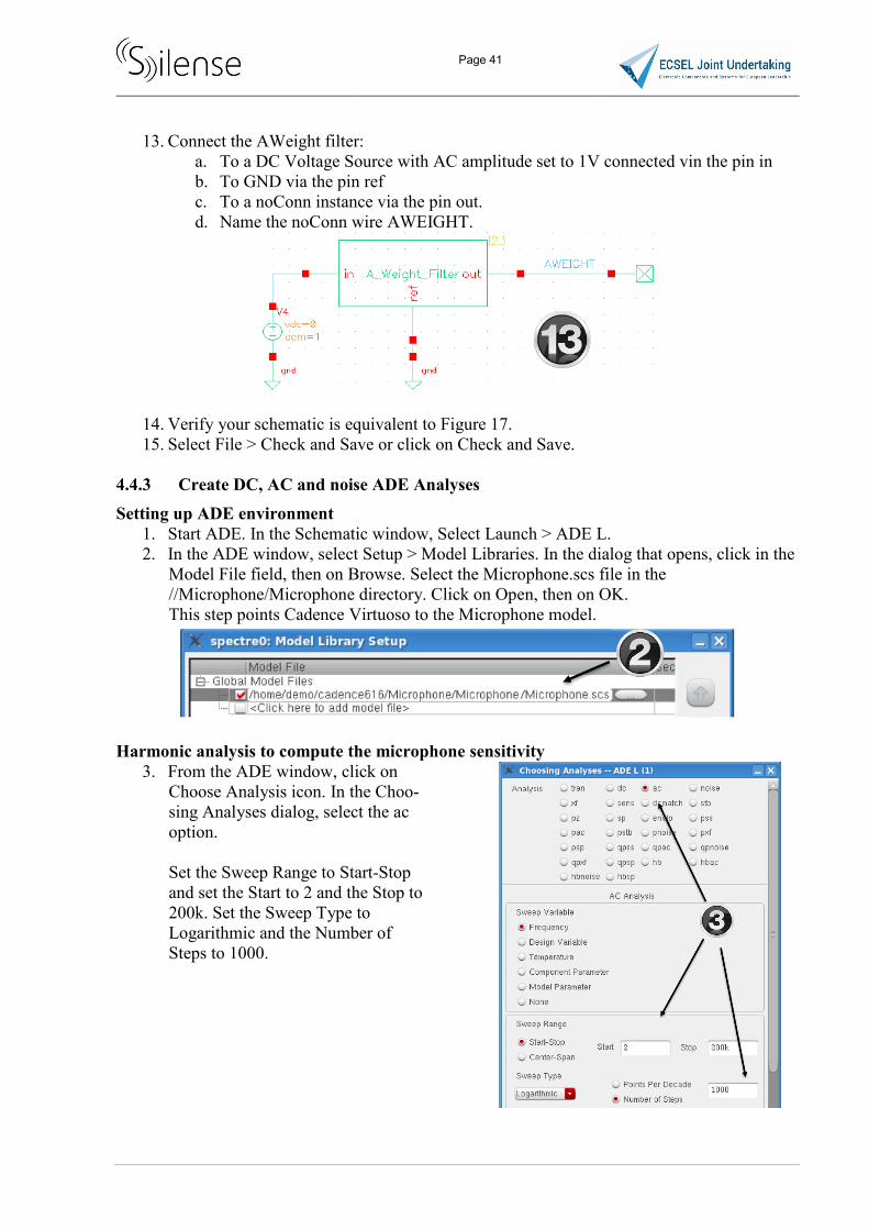
13. Connect the AWeight filter: a. To a DC Voltage Source with AC amplitude set to 1V connected vin the pin in b. To GND via the pin ref c. To a noConn instance via the pin out. d. Name the noConn wire AWEIGHT.
14. Verify your schematic is equivalent to Figure 17. 15. Select File > Check and Save or click on Check and Save.
4.4.3 Create DC, AC and noise ADE Analyses Setting up ADE environment
1. Start ADE. In the Schematic window, Select Launch > ADE L. 2. In the ADE window, select Setup > Model Libraries. In the dialog that opens, click in the
Model File field, then on Browse. Select the Microphone.scs file in the //Microphone/Microphone directory. Click on Open, then on OK. This step points Cadence Virtuoso to the Microphone model.
Harmonic analysis to compute the microphone sensitivity
3. From the ADE window, click on Choose Analysis icon. In the Choo-sing Analyses dialog, select the ac option.
Set the Sweep Range to Start-Stop and set the Start to 2 and the Stop to 200k. Set the Sweep Type to Logarithmic and the Number of Steps to 1000.
Page 42
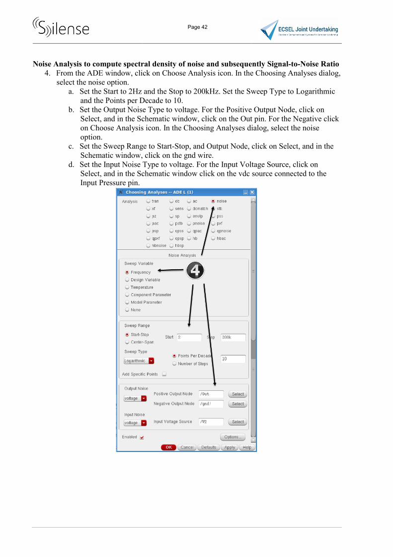
Noise Analysis to compute spectral density of noise and subsequently Signal-to-Noise Ratio 4. From the ADE window, click on Choose Analysis icon. In the Choosing Analyses dialog,
select the noise option. a. Set the Start to 2Hz and the Stop to 200kHz. Set the Sweep Type to Logarithmic
and the Points per Decade to 10. b. Set the Output Noise Type to voltage. For the Positive Output Node, click on
Select, and in the Schematic window, click on the Out pin. For the Negative click on Choose Analysis icon. In the Choosing Analyses dialog, select the noise option.
c. Set the Sweep Range to Start-Stop, and Output Node, click on Select, and in the Schematic window, click on the gnd wire.
d. Set the Input Noise Type to voltage. For the Input Voltage Source, click on Select, and in the Schematic window click on the vdc source connected to the Input Pressure pin.

Page 43
4.4.4 Simulation post-processing: Sensitivity and SNR calculation Sets ADE Outputs / Run Simulations / Post process results
1. Right Click in the Design Variables pane and select Copy From Cellview. 2. Set the variable as follows:
a. C_Parasitic = 0 b. V_Bias = 5 c. R_Load = 100G d. R_Leakage = 10T
3. Right Click in the Outputs pane of ADE and select Edit.
4. Add the 5 following signals: a. Name: Plot A-Weighted Curve,
Expression: dB20(mag(getData(“ /AWEIGHT” ?result “ac-ac”))) b. Name: Sensitivity Plot (dBV)
Expression: dB20(mag(getData(“/out” ?result “ac-ac”))) c. Sensitivity at 1 kHz (dBV)
Expression: dB20(value(mag(getData(“/out” ?result “ac-ac”)) 1000)) d. Noise Plot (V/sqrt(Hz))
Expression: getData(“out” ?result “noise) e. A-Weighted Signal-to-Noise Ratio (dBa)
Expression: dB20((value(mag(getData(“/out” ?result “ac-ac”)) 1000) / sqrt(integ(((mag(getData(“/AWEIGHT” ?result “ac-ac”)) * mag(getData(“out” ?result “noise”)))**2) 20 20000))))
Page 44
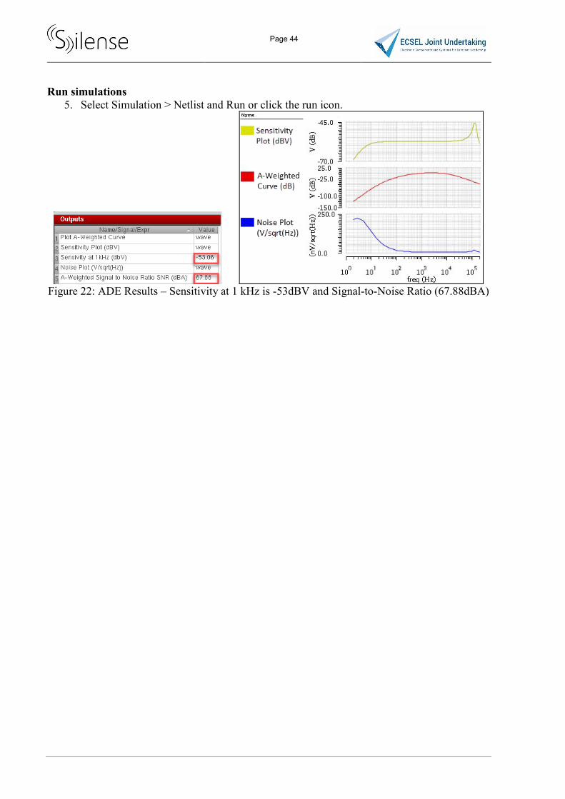
Run simulations 5. Select Simulation > Netlist and Run or click the run icon.
Figure 22: ADE Results – Sensitivity at 1 kHz is -53dBV and Signal-to-Noise Ratio (67.88dBA)
Page 45
5 COVENTORWARE SIMULATION VERIFICATION In this section we will export the model from MEMS+ to CoventorWare to compare the predicted behavior between the two tools, i.e. high order finite elements in MEMS+ and low order conventional finite elements in CoventorWare. In all cases we show the results between the two approaches match well. The model can be exported from MEMS+ either as a GDS file or as a solid model (SAT) file. The SAT files can be meshed directly whereas the GDS is used to recreate a SAT model from a process description in CoventorWare.
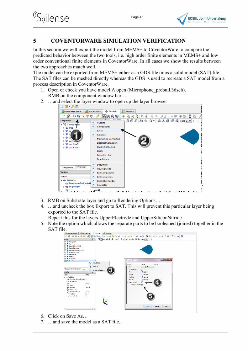
1. Open or check you have model A open (Microphone_prebuil.3dsch). RMB on the component window bar…
2. …and select the layer window to open up the layer browser
3. RMB on Substrate layer and go to Rendering Options… 4. …and uncheck the box Export to SAT. This will prevent this particular layer being
exported to the SAT file. Repeat this for the layers UpperElectrode and UpperSiliconNitride
5. Note the option which allows the separate parts to be booleaned (joined) together in the SAT file.
6. Click on Save As… 7. …and save the model as a SAT file...

Page 46
8. …and GDS file. These files can now be imported into other CAD tools including CoventorWare.
Page 47
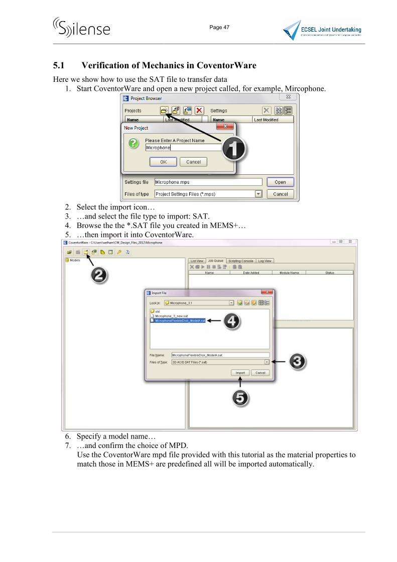
5.1 Verification of Mechanics in CoventorWare Here we show how to use the SAT file to transfer data
1. Start CoventorWare and open a new project called, for example, Mircophone.
2. Select the import icon… 3. …and select the file type to import: SAT. 4. Browse the the *.SAT file you created in MEMS+… 5. …then import it into CoventorWare.
6. Specify a model name… 7. …and confirm the choice of MPD.
Use the CoventorWare mpd file provided with this tutorial as the material properties to match those in MEMS+ are predefined all will be imported automatically.
Page 48
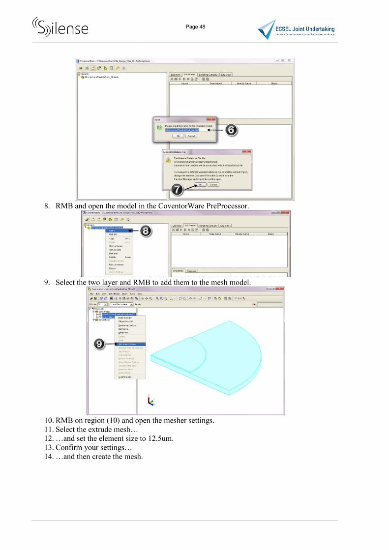
8. RMB and open the model in the CoventorWare PreProcessor.
9. Select the two layer and RMB to add them to the mesh model.
10. RMB on region (10) and open the mesher settings. 11. Select the extrude mesh… 12. …and set the element size to 12.5um. 13. Confirm your settings… 14. …and then create the mesh.

Page 49
15. Set the patch names and then save the model.
Note, for clarity the mesh and top surfaces are not visible in the image. It is also scaled in Z (by 200). The model can now be simulated in MemMech…
5.1.1 Stress deformation
16. In the CoventorWare consol RMB on the model and set a new analysis. 17. Select MemMech and proceed to the surface boundary conditions table… 18. …and set the conditions shown opposite.
Here, the outer edge of the membrane is fixed, and the straight edges restrained to respect the quarter symmetry of the model.

Page 50
19. When the simulation has completed, load the 3D results into CoventorWare Post-
Processor. The 2D results table gives a maximum displacement magnitude of 0.0279 um. Note, ideally, a mesh study should be performed to gauge the effect of mesh density on the result.
20. Re-run the dc analysis with no bias in MEMS+ and check the d.c. displacement, it should match at 0.029 um (20)

Page 51
5.1.2 Mode Frequencies As well as the static displacement the mode frequencies can be compared. Table 1 compares the mode frequencies from MEMS+ (optimized model) with those from the CoventorWare model described above.
Table 1: Mode frequencies, MEMS+ optimized and CoventorWare
Page 52
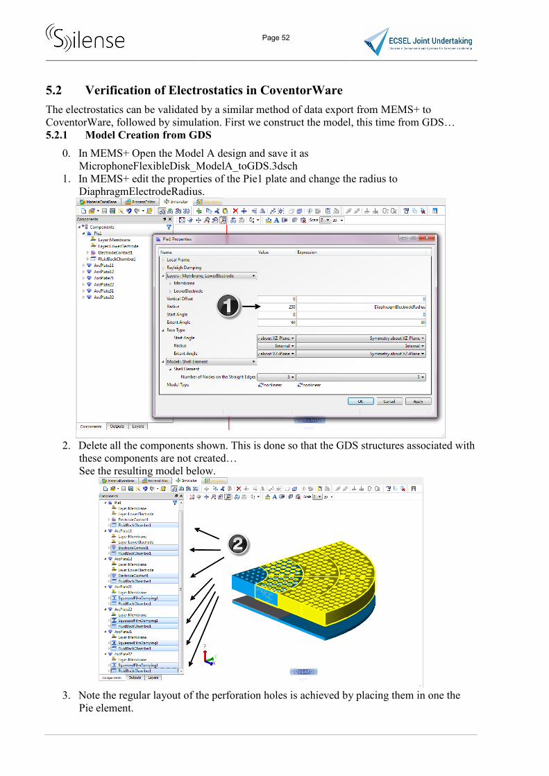
5.2 Verification of Electrostatics in CoventorWare The electrostatics can be validated by a similar method of data export from MEMS+ to CoventorWare, followed by simulation. First we construct the model, this time from GDS… 5.2.1 Model Creation from GDS
0. In MEMS+ Open the Model A design and save it as MicrophoneFlexibleDisk_ModelA_toGDS.3dsch
1. In MEMS+ edit the properties of the Pie1 plate and change the radius to DiaphragmElectrodeRadius.
2. Delete all the components shown. This is done so that the GDS structures associated with
these components are not created… See the resulting model below.
3. Note the regular layout of the perforation holes is achieved by placing them in one the
Pie element.
Page 53
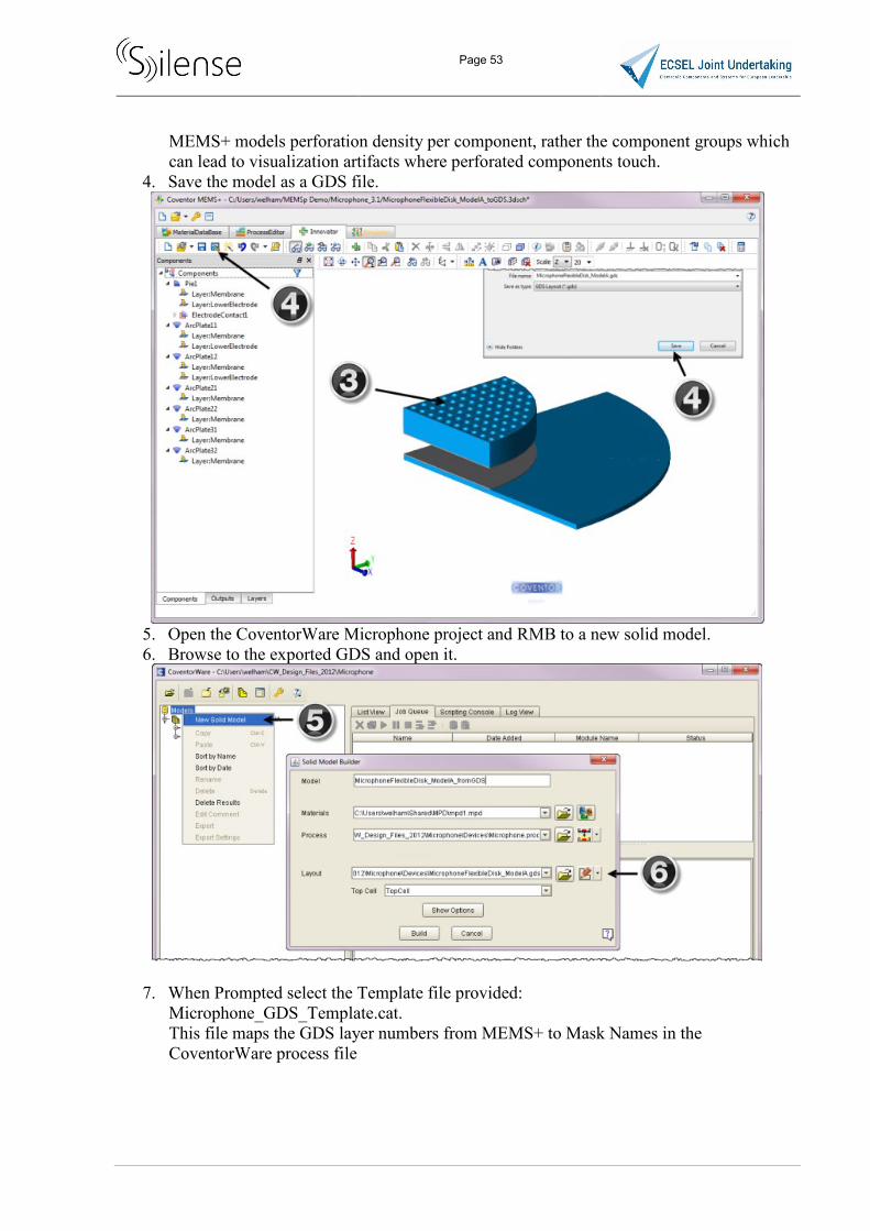
MEMS+ models perforation density per component, rather the component groups which can lead to visualization artifacts where perforated components touch.
4. Save the model as a GDS file.
5. Open the CoventorWare Microphone project and RMB to a new solid model. 6. Browse to the exported GDS and open it.
7. When Prompted select the Template file provided: Microphone_GDS_Template.cat. This file maps the GDS layer numbers from MEMS+ to Mask Names in the CoventorWare process file
Page 54
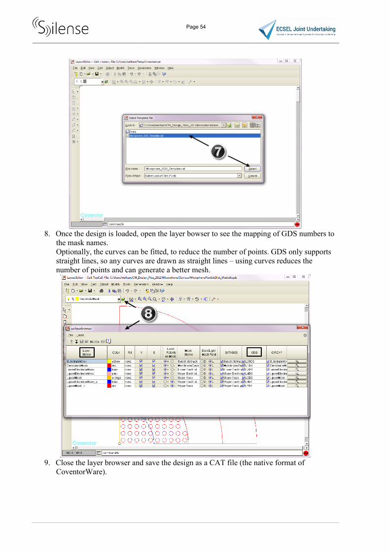
8. Once the design is loaded, open the layer bowser to see the mapping of GDS numbers to
the mask names. Optionally, the curves can be fitted, to reduce the number of points. GDS only supports straight lines, so any curves are drawn as straight lines – using curves reduces the number of points and can generate a better mesh.
9. Close the layer browser and save the design as a CAT file (the native format of
CoventorWare).
Page 55
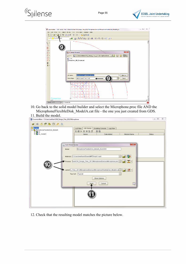
10. Go back to the solid model builder and select the Microphone.proc file AND the
MicrophoneFlexibleDisk_ModelA.cat file - the one you just created from GDS. 11. Build the model.
12. Check that the resulting model matches the picture below.

Page 56
13. To model the quarter symmetry in both the electrostatic domain and mechanical domain
add a Wedge. Once the wedge is meshed it will apply symmetry conditions for both electrostatics and mechanics.
14. Add all the layers, including the wedge, to the mesh model. Do not add the substrate.

Page 57
15. Scale the model in Z by 500. 16. Using “box select” (shift and LMB) select all the external patches on the membrane edge
Make sure these are the only patches selected. Set the name to fixAll. Note – scaling in Z helps to select the patches.
17. Create an extrude mesh on the backplate and membrane using the settings shown below.

Page 58
18. Create a surface mesh for the symmetry planes.
19. Check your mesh looks the same as in the image below and rename the conductor names.
20. Finally, select the backplate layers and RMB to set the selection Supress, Except
MemElectro. Save the model. Supressed parts will not be seen by the mechanical solver resulting is reduced simulation time. Here, they are considered rigid so this setting is acceptable.
Page 59
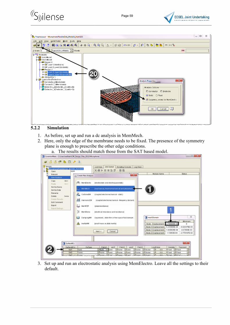
5.2.2 Simulation
1. As before, set up and run a dc analysis in MemMech. 2. Here, only the edge of the membrane needs to be fixed. The presence of the symmetry
plane is enough to prescribe the other edge conditions. a. The results should match those from the SAT based model.
3. Set up and run an electrostatic analysis using MemElectro. Leave all the settings to their
default.

Page 60
4. Check the capacitance in the result table, it should be 0.185pF for the quarter model.
The full model will be 4 times this value. Note, ideally, a mesh study should be performed to gauge the effect of mesh density on the result.
5. Go back to MEMS+, add and run a dc analysis (no bias). Open the result in Scene3D
viewer (double click). In the results viewer plot the output capacitance – there is only one value as it is a dc. simulation. Add a data label. The result is 0.186pF compared to the CoventorWare value of 0.185pF
Page 61
5.2.3 Verification of Coupled Electrostatics-Mechanics in CoventorWare
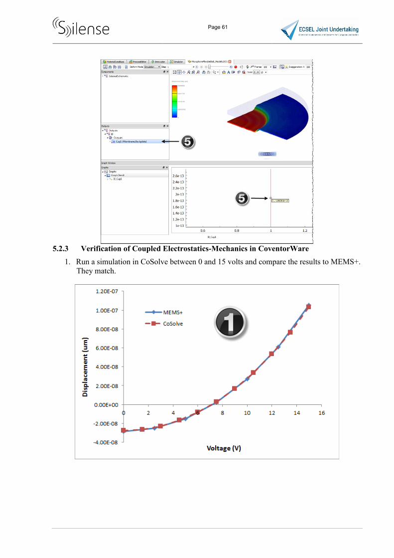
1. Run a simulation in CoSolve between 0 and 15 volts and compare the results to MEMS+. They match.

Page 62
6 REFERENCES [1] M. Royer, J. O. Holmen, M. A. Wurm, O. S. Aadland and M. Glenn, "ZnO on Si integrated
acoustic sensor," Sensors and Actuators A, vol. 4, pp. 357-362, 1983. [2] M. Pedersen, W. Olthuis and P. Bergveld, "A silicon condenser microphone wih polyimide
diaphragm and backplate," Sensors and Actuators A, vol. 63, pp. 97-104, 1997. [3] A. Torkkeli, H. Sipola, H. Sepa, J. Saarilahti, O. Rusanen and J. Hietanen, "Capacitive
Microphone with Low-stress Polysilicon Membrane and High-stress Polysilicon Backplate," in Eurosensors XIII, The Hague, The Netherlands, 1999.
[4] M. Sheplak and J. Seiner, "A MEMS Microphone for Aeroacoustics Measurements," in 37th AIAA Aerospace Sciences Meeting & Exhibit, -, 1999.
[5] J. Lewis, "Understanding Microphone Sensitivity," Analog Devices, 2004. [Online]. Available: http://www.analog.com/en/analog-dialogue/articles/understanding-microphone-sensitivity.html.
[6] S. A. Jawel, CMOS Readout Interfaces for MEMS Capacitive Microphones,, PhD Thesis, 2009.
[7] A. Cheng, Design of a Readout Scheme for a MEMS Microphone, Master of Science Thesis, 2009.
[8] Wikipedia, "A-weighting," Wikimedia, [Online]. Available: https://en.wikipedia.org/wiki/A-weighting.
[9] D. Cattin, Design, Modelling and Control of IRST Capacitive Mems Microphone, PhD Thesis, 2009.
[10] Anlog Devices, "Microphone Specifications Explained," ADI, 2011. [Online]. Available: https://wiki.analog.com/resources/app-notes/an-1112.
[11] I. Williams, "Noise - 2," Texas Instruments - Precision Labs, 2015. [Online]. Available: https://training.ti.com/system/files/docs/1312%20-%20Noise%202%20-%20slides.pdf.
[12] Verilog-A, Language Reference Manual, Open Verilog International, 1996. [13] M. S. Floater and K. Hormann, "Barycentric rational interpolation with no poles and high
rates of approximation," NumerischeMathematik, vol. 107, pp. 315-331, 2007. [14] R. Kressmann, M. Klaiber and G. Hess, "Silicon Condenser microphones with corrugated
siliconoxide/nitride electret membranes," Sensors and Actuators A, vol. 100, pp. 301-309, 2002.
[15] P. R. Scheeper, W. Olthuis and P. Bergvwld, "he design, fabricatation and testing of corru-gated silicon nitride diaphragms," IEEE J. Microelectromech. Syst., vol. 13, pp. 36-42, 1994.