report on the radiation hardness tests developed for the...
TRANSCRIPT

Report on the radiation hardness testsdeveloped for the PAMELA experiment
September 2002
In the last years several tests have been carried out to measure radiation hardness of theelectronic components of the PAMELA experiment. A large number of devices have beentested and two different categories of experiments can be distinguished, on the basis of theeffect to be stressed:
1. test for Total Ionising Dose (TID);
2. test for Single Event Effects (SEE), Upset (SEU) or Latch–up (SEL).
In order to estimate the total dose of radiation during the mission on satellite, simulationsby means of the CREME96 software have been performed. This program, available onlineat [1], is designed to study the effect of radiation in space on microelectronic devices: it takesinto account the contributions coming from
� protons and heavy nuclei, both of cosmic origin and trapped in the radiation beltsaround the Earth;
� protons and heavy nuclei emitted during solar flares, whose flux changes in differentphases of the solar cycle.
In figure 1 the flux of particles impinging on the PAMELA apparatus, as calculated byCREME96, is reported. This calculation has been carried out taking into accont the orbitalconditions of the satellite and the metallic shield around the detector (2 mm of Al). The solarparticles contribution has been evaluated using the incoming flux in the worst week of thelast solar cycle. As we can see, the solar activity increases flux at low energies. Solar activitycan also change the field into the magnetosphere, reducing the magnetic screen around theEarth for cosmic particles.
For a three year mission at 300–600 km of altitude and 70.4�
of inclination a 1 kradtotal dose on the apparatus has been estimated using CREME96 and assuming the solarflux equivalent to that obtained in 10 days with intensity of the worst week (see figure 1).
Test for Total Ionising Dose. The first class of tests has been done in 1999 at the researchcenter of Casaccia (Roma), by irradiating electronics components with a � source. It wasa high intensity ( ������� ��� Bq) ��� Co emitter. The decay scheme of this isotope is shown infigure 2. For our purposes we can consider that a couple of 1.25 MeV � rays are emitted
1

Kinetic energy (MeV/nucleon)
Diff
eren
tial f
lux
(par
ticle
s (m
2 s sr
MeV
/nuc
leon
)-1)
10-14
10-12
10-10
10-8
10-6
10-4
10-2
1
10 2
10 4
10 6
1 10 102
103
104
105
Figure 1: Main contributions of cosmic rays and solar particles (averaged on 200 orbits) tothe differential flux of particles on the PAMELA detector. The solar contribution is calcu-lated in the worst week of the last cycle of the Sun.
Figure 2: Decay scheme of ��� Co. The mean energy of a � ray is 1.25 MeV.
2

Ionizing radiation dose (Rad)
Loss
of r
eman
ence
(dB
r / B
r)
0
0.01
0.02
0.03
0.04
0.05
107
108
109
Figure 3: Effects of ionizing radiation on the remanence ��� of Nd–Fe–B material. Thisfigure is taken from [2].
in each decay. At this energy the predominant interaction mechanism is Compton effect. Inaddition, by using a � –ray source instead of charged particles, the energy deposit is due tosecondary electrons and it is more uniform in the sensitive volume and less intense.
In the irradiation phase, the source is extracted from the deep well where is usually keptfor reasons of security and placed near objects to be irradiated for a suitable amount of time.Tests of functionality of the chips have been performed when doses of 1, 2, 10, 30 krad werereached. The final dose 30 krad is about 30 times greater with respect to that expected forthe PAMELA mission. A list of the tested chip is given in Appendix I, where results of theirradiation are reported: four components showed a failure.
Obviously in all the boards realized for the flight model of the detector only componentsthat passed successfully this test and the subsequent ones have been employed.
For what concerns the material constituting the permanent magnet of the tracking system,some works have been found in literature where irradiation tests of such materials wereperformed. In the reference [2] the Nd–Fe–B alloy (which composes the PAMELA magnet)has been subjected to irradiation at very high doses and no significant effects are reported.Figure 3, taken from this paper, shows that the remanence ��� has only a small variation( � 5%) observed for doses five orders of magnitude larger with respect to those expected inthree years in orbit.
Other tests have been performed at Casaccia in 2002, both concerning electronic com-
3

ponents (also listed in Appendix I) and the magnetic screens to be positioned around themagnet. The irradiation test of the magnetic screens has been performed in three steps:
� A system composed of one PAMELA magnet module and four screens has been as-sembled. The main axis (where the magnetic field is greater) is called � axis. Theexternal magnetic field along � axis has been measured in different points by meansof a hand Hall probe.
� The magnetic screens have been irradiated at a total dose level of 10 krad.
� The field along the � axis has been newly measured in the same positions and bymeans of the same probe as already done before the irradiation.
The results of these measurements, reported in Appendix III, show no difference in the fieldintensity.
Test for Single Event Upset and Latch–up. In the period 2000–2002 three beam testsessions have been developed at GSI [3] and two in Dubna [4]. High Z nuclei have beenutilized from these facitilies in order to study upset and latch–up for some chips.
COUNTER 1
FPGA under test
COMPARATORPROCESSOR
current SENSOR
reset
u
l
COUNTER 2
Figure 4: Scheme of the circuit for SEU/SEL detection at GSI.
� Upset is the inversion of the logic state of a memory cell which causes loss of infor-mation contained in.
� Latch–up is the activation of a conduction channel inside the chip. In this case theabsorbed current increases and the chip can be permanently damaged if high tempera-tures are reached, so to fuse the ohmic contacts. A protection circuit, which can switchoff the power supply when the current becomes greater than a given limit, has to beforeseen to avoid damage.
4

At GSI in November 2000 beams of Xenon and Uranium were available for such type ofstudies. The energy deposition is usually measured giving the Linear Energy Transfer of theparticle (LET)1 when it enter a material. Available energies were 100 to 800 MeV/ � at angles0, 30, 60 deg., corresponding to Effective LET values in the range 5–70 MeV cm � /mg.
We tested two FPGA chips, namely QuickLogic QL12x16BL and Actel 54SX32. Inorder to perform a significant test, these chips have been mounted as piggy-back on a boardwhere they could be controlled by a microprocessor (DSP). On each FPGA two identicalcounters, driven by a clock signal from DSP, have been built (see scheme in figure 4). Thesecounters, at the same time, have to give the same progressive number, if no upset occurs inthe memory cells. On the same chip a comparator reads the values given by these counters:when a difference is found, a signal � (see figure) is sent to DSP and it increases the internalSEU counter. Latch–up is detected monitoring the current flowing in the chip. Cross sectionsfor single event effect (upset or latch–up) are reported in figure 4 for both chips.
These results can be enumerated:
� measured cross section for Actel chip is lower: so this chip family has been chosen foruse in control logic;
� Actel 54SX32, unlike Quick Logic chip, showed no latch–up, the more dangerouseffect;
� the cross section for Actel can be used as input of the CREME96 program; by simulat-ing fluxes of protons and high Z nuclei, rates of SEE can be determined. On the orbitof PAMELA the following error rates can be estimated, taking into account the totalnumber of such devices in the telescope:
a) galactic + trapped particles: ���������� !� SEU/dayb) solar particles: ������! !" SEU/day
The a) contribution has to be multiplied approximately for 1000 days to obtain thetotal rate, while b) for only 10 days. So they become of the same order of magnitude,i.e. �� !� SEU for these chips in the whole apparatus in three years. Little variationsto these values have to be taken into account, because the SEU rates depend on thenumber of bits utilized in the FPGA.
In the same and subsequent test sessions at GSI other components have been tested in asimilar manner and all the tested components are enumerated in Appendix II.
In Dubna, at Nuclotron facility, a �$# Mg beam was employed for SEU/SEL tests in De-cember 2001. The beam energy was 150 MeV/ � , corresponding to LET of about 1 MeVcm � /mg on the sensitive part of the chip (after crossing dead layers).
1The LET is equivalent to % dE/( & dx) of the Bethe–Bloch formula. The Effective LET takes into accountthe angle of incidence ' of the particles and it is equal to LET divided by (*),+-' .
5

10-7
10-6
10-5
10-4
10-3
10-2
20 30 40 50 60 70 80
Effective LET (MeV cm2 mg-1)
Cro
ss s
ectio
n (c
m2 /d
evic
e)
Effective LET (MeV cm2 mg-1)
Cro
ss s
ectio
n (c
m2 /d
evic
e)
10-7
10-6
10-5
10-4
10-3
10-2
20 30 40 50 60 70 80
Figure 5: Cross sections for single event effect (upset or latch–up) incm � device .� , measured at GSI for two FPGA chips.
6

A 1 Mbit flash memory chip (mod. M25P10 manufactured by ST Microelectronics) hasbeen tested filling all the memory cells with a sequence of ’1’ and checking continuously ifsome ’0’ appeared. In this case a SEU counter was increased and the bulk erase of the chiprepeated. Latch–up was monitored through the current passing in the chip and a protectioncircuit prevented permanent damages.
All the other components were tested only for latch–up, checking their functionalityduring the irradiation and after. Two DC/DC converter boards, mod. S9004 and S9006,manufactured by CAEN as power supplies for analogic and digital electronics of PAMELAwere subject of investigation. Both the boards have an input voltage in the range 15–20 V andthe output is 5.6 V and 3.4 V respectively. On each board some chips have been irradiated,continuously checking the output voltage of the board.
A MOSFET failed on S9006 board: the output voltage of the DC/DC converter switchedoff during the irradiation of this component and could not be restored.
As a consequence of this failure, in February 2002 at Nuclotron and in May 2002 at GSIother power MOSFETs have been extensively tested for latch–up. A 100 MeV/ �/�$# Mg beamhas been used in the first test. In the second one, a 900–150 MeV/ �0��"�1 U beam was presentinstead: the high energy transfer of such particles produced failures on some chips that hadpassed successfully the Nuclotron run. In the test procedure each MOS (built to work at 100or 150 V) was subject to a power supply of 40, 70 and 100 V during the irradiation and theabsorbed current was checked.
Also these chips tested at Dubna and GSI are listed in Appendix II, where permanentdamages to the chips are reported.
Conclusions. As a result of all the test performed on the electronics of PAMELA we canbe confident that no failure can result during the mission on satellite, both for total dose andfor latch–up. Also results of SEU test are encouraging, because threshold for this process indigital components corresponds to high values of the energy transfer. In fact, by simulatinga LET spectrum in orbit we found that the fraction of the spectrum above SEU–threshold isvery small. In addition, protection circuits for latch–up have been introduced where possibleand redundancies have been foreseen to avoid loss of information caused by upsets.
7
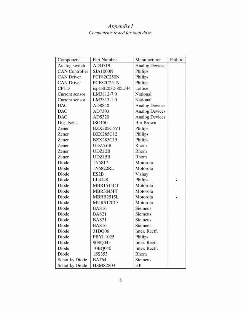
Appendix IComponents tested for total dose.
Component Part Number Manufacturer FailureAnalog switch ADG719 Analog DevicesCAN Controller SJA1000N PhilipsCAN Driver PCF82C250N PhilipsCAN Driver PCF82C251N PhilipsCPLD ispLSI2032-80LJ44 LatticeCurrent sensor LM3812-7.0 NationalCurrent sensor LM3813-1.0 NationalDAC AD8840 Analog DevicesDAC AD7303 Analog DevicesDAC AD5320 Analog DevicesDig. Isolat. ISO150 Bur BrownZener BZX285C5V1 PhilipsZener BZX285C12 PhilipsZener BZX285C15 PhilipsZener UDZ5.6B RhomZener UDZ12B RhomZener UDZ15B RhomDiode 1N5817 MotorolaDiode 1N5822RL MotorolaDiode ES2B VishayDiode LL4148 Philips 2Diode MBR1545CT MotorolaDiode MBR3045PT MotorolaDiode MBRB2515L Motorola 2Diode MURS120T3 MotorolaDiode BAS16 SiemensDiode BAS21 SiemensDiode BAS21 SiemensDiode BAS16 SiemensDiode 31DQ06 Inter. Rectf.Diode PBYL1025 PhilipsDiode 90SQ045 Inter. Rectf.Diode 10BQ040 Inter. Rectf.Diode 1SS353 RhomSchottky Diode BAT64 SiemensSchottky Diode HSMS2803 HP
8

Component Part Number Manufacturer FailureDSP ADSP-2187L Analog DevicesDSP ADSP-2185L Analog DevicesDSP ADSP-2189MBST-266 Analog DevicesFlash EEPROM Am29F010-120 AMDIsolator ISO508 Burr-BrownIsolator ISO518 Burr-BrownIsolator ISO422 Burr-BrownLinear Regulator LM2941T NationalLinear Regulator LP2952IN NationalLinear Regulator TPS76701QD Texas 2Linear Regulator LM2940CT-5.0 NationalLinear Regulator LM2991T NationalLinear Regulator LX8941CP LinfinityLinear Regulator LX8940CP LinfinityLinear Regulator LX8586A(6A) LinfinityMOS N–channel MTD20N06HD MotorolaMOS N–channel SI4810DY VishayMOS N–channel FDS9936A FairchildMOS N–channel FDS6680A FairchildMOS N–channel FDS6612A FairchildMOS N–channel FDS6690A FairchildMOS N–channel SUP60N06 VishayMOS N–channel SI4466DY VishayMOS N–channel IRF540 Inter. Rectf.MOS N–channel IRF640 Inter. Rectf.MOS N–channel IRF740 Inter. Rectf.MOS P–channel NDP6020P MotorolaOperational LT1014DN Linear Tech 2Operational OP471G Analog DevicesOperational LF347BN NationalOperational LM6142AIN NationalOperational LT1366CN8 Linear TechOperational OP17GZ Analog DevicesOperational OP249AZ Analog DevicesOperational OP42G Analog DevicesOperational AD713BQ Analog DevicesOptocoupler PC905Y SharpOptocoupler MOC207 SiemensOptocoupler SFH6186-5 HP
9

Component Part Number Manufacturer FailureLinear regulator 100V S9001 CAENTemperature sensor DS1820 DallasBipolar Transistor MMBTA42 MotorolaBipolar Transistor MMBTA92 MotorolaBipolar Transistor 2N5401 MotorolaBipolar Transistor 2N5551 MotorolaBipolar Transistor BD433 PhilipsBipolar Transistor BD434 PhilipsBipolar Transistor MJD200 MotorolaBipolar Transistor MJD210 MotorolaBipolar Transistor MJE340 MotorolaBipolar Transistor MJE350 MotorolaBipolar Transistor MMBT3904LT1 MotorolaBipolar Transistor MMBT3906LT1 MotorolaVoltage Ref. LM185H-1.2 NationalVoltage Ref. LM4040CIM3-10.0 NationalVoltage Ref. LM4040BIM3-5.0 NationalCMOS DS90LV027A NationalCMOS DS90LV028A NationalCMOS DS90LV047A NationalCMOS DS90LV048A NationalOscillator CX03M 25 MHz StatekOscillator CX03M 40 MHz StatekTemperature sensor AD590 Analog DevicesB field sensor BH203 BellLinear regulator LX8941 Linfinity 2 (30 krad)
10

Appendix IIComponents tested for SEU/SEL.
Component Part Number Manufacturer Test session Permanentdamage
Digital Coupler ADuM1100 Analog Devices GSI 2000VA-chip VA 32 old Ideas GSI 2000VA-chip VA 32 new Ideas GSI 2000PGA QL12 � 16BL QuickLogic GSI 2000FPGA 54SX32 Actel GSI 2000ADC AD7476 Analog Devices GSI 2001DSP ADSP2187L Analog Devices GSI 2001PGA 54SX32A Actel GSI 2001Flash Memory AM29LV004 AMD GSI 2001Mosfet N channel HUF76629D3S Fairchild GSI 2002 2Mosfet N channel IRFR18N15D I.R. GSI 2002Mosfet N channel FDD2570 Fairchild GSI 2002Mosfet N channel FDD3670 Fairchild GSI 2002 2Flash Memory M25P10 ST Dubna 2001Mosfet P channel IRFR5305 Digi–key Dubna 2001Transistor array MMPQ3906 Fairchild Dubna 2001Quad Comparator LM239 National Dubna 2001Optocoupler OLS303-SB Isolink Dubna 2001Shunt regulator TL431 Fairchild Dubna 2001Mosfet N channel SUB60N06-18 Vishay Dubna 2001PWM controller UC2843AD8 Texas Dubna 2001BJT NPN FZT605 Zetex Dubna 2001Mosfet N channel MTD20N06HD ON Dubna 2001 2Mosfet N channel IRFR3910 I.R. Dubna 2002Mosfet N channel IRFZ44ES I.R. Dubna 2002Mosfet N channel HUF76629D3S Intersil Dubna 2002Mosfet N channel SPB11N60S5 Infineon Dubna 2002Mosfet N channel SPB20N60S5E3045 Infineon Dubna 2002Mosfet N channel IRFR18N15D I.R. Dubna 2002Mosfet N channel IRFR2407 I.R. Dubna 2002Mosfet N channel IRFR13N15 I.R. Dubna 2002Mosfet N channel IRFR15N20 I.R. Dubna 2002Mosfet N channel SPD30N08S2L-21 Infineon Dubna 2002Mosfet N channel SPD30N08S2-22 Infineon Dubna 2002Mosfet N channel MTD20N06HD Motorola Dubna 2002Mosfet N channel RFP40N10 Intersil Dubna 2002Mosfet N channel HUF76619D3S Intersil Dubna 2002
11

Appendix IIITest of the magnetic screens:
measurement of intensity before and after the irradiation.
Distance from the screen B before the irradiation B after the irradiation(mm) (mT) (mT)
60 1.96 1.9580 1.57 1.57
100 1.26 1.27120 1.01 1.02140 0.81 0.80160 0.65 0.64180 0.53 0.52200 0.44 0.42220 0.35 0.35240 0.28 0.29260 0.24 0.24280 0.20 0.19300 0.17 0.17
12

Bibliography
[1] http://crsp3.nrl.navy.mil/creme96
[2] W. V. Hassenzahl et al., NIM A291 (1990) 378-382
[3] http://www.gsi.de
[4] http://www.jinr.ru
13