renesas synergy development kit dk-s7g2 user's …€™s manual renesas synergy development...
TRANSCRIPT

User’s M
anual
Renesas Synergy™Development Kit DK-S7G2 v3.0
User’s Manual
Synergy S7G2 MCU
All information contained in these materials, including products and product specifications, represents information on the product at the time of publication and is subject to change by Renesas Electronics Corp. without notice. Please review the latest information published by Renesas Electronics Corp. through various means, including the Renesas Electronics Corp. website (http://www.renesas.com).

Legal Notice
1) Descriptions of circuits, software and other related information in this document are provided only to illustrate the operation of semiconductor products and application examples. You are fully responsible for the incorporation of these circuits, software, and information in the design of your equipment. Renesas Electronics assumes no responsibility for any losses incurred by you or third parties arising from the use of these circuits, software, or information.
2) Renesas Electronics has used reasonable care in preparing the information included in this document, but Renesas Electronics does not warrant that such information is error free. Renesas Electronics assumes no liability whatsoever for any damages incurred by you resulting from errors in or omissions from the information included herein.
3) Renesas Electronics does not assume any liability for infringement of patents, copyrights, or other intellectual property rights of third parties by or arising from the use of Renesas Electronics products or technical information described in this document. No license, express, implied or otherwise, is granted hereby under any patents, copyrights or other intellectual property rights of Renesas Electronics or others.
4) You should not alter, modify, copy, or otherwise misappropriate any Renesas Electronics product, whether in whole or in part. Renesas Electronics assumes no responsibility for any losses incurred by you or third parties arising from such alteration, modification, copy or otherwise misappropriation of Renesas Electronics product.
5) Renesas Electronics products are classified according to the following two quality grades: “Standard” and “High Quality”. The recommended applications for each Renesas Electronics product depends on the product’s quality grade, as indicated below.
“Standard”: Computers; office equipment; communications equipment; test and measurement equipment; audio and visual equipment; home electronic appliances; machine tools; personal electronic equipment; and industrial robots etc.
“High Quality”: Transportation equipment (automobiles, trains, ships, etc.); traffic control systems; anti-disaster systems; anticrime systems; and safety equipment etc.
Renesas Electronics products are neither intended nor authorized for use in products or systems that may pose a direct threat to human life or bodily injury (artificial life support devices or systems, surgical implantations etc.), or may cause serious property damages (nuclear reactor control systems, military equipment etc.). You must check the quality grade of each Renesas Electronics product before using it in a particular application. You may not use any Renesas Electronics product for any application for which it is not intended. Renesas Electronics shall not be in any way liable for any damages or losses incurred by you or third parties arising from the use of any Renesas Electronics product for which the product is not intended by Renesas Electronics.
6) You should use the Renesas Electronics products described in this document within the range specified by Renesas Electronics, especially with respect to the maximum rating, operating supply voltage range, movement power voltage range, heat radiation characteristics, installation and other product characteristics. Renesas Electronics shall have no liability for malfunctions or damages arising out of the use of Renesas Electronics products beyond such specified ranges.
7) Although Renesas Electronics endeavors to improve the quality and reliability of its products, semiconductor products have specific characteristics such as the occurrence of failure at a certain rate and malfunctions under certain use condi-tions. Further, Renesas Electronics products are not subject to radiation resistance design. Please be sure to implement safety measures to guard them against the possibility of physical injury, and injury or damage caused by fire in the event of the failure of a Renesas Electronics product, such as safety design for hardware and software including but not limited to redundancy, fire control and malfunction prevention, appropriate treatment for aging degradation or any other appro-priate measures. Because the evaluation of microcomputer software alone is very difficult, please evaluate the safety of the final products or systems manufactured by you.
8) Please contact a Renesas Electronics sales office for details as to environmental matters such as the environmental compatibility of each Renesas Electronics product. Please use Renesas Electronics products in compliance with all applicable laws and regulations that regulate the inclusion or use of controlled substances, including without limitation, the EU RoHS Directive. Renesas Electronics assumes no liability for damages or losses occurring as a result of your noncompliance with applicable laws and regulations.
9) Renesas Electronics products and technology may not be used for or incorporated into any products or systems whose manufacture, use, or sale is prohibited under any applicable domestic or foreign laws or regulations. You should not use Renesas Electronics products or technology described in this document for any purpose relating to military applications

or use by the military, including but not limited to the development of weapons of mass destruction. When exporting the Renesas Electronics products or technology described in this document, you should comply with the applicable export control laws and regulations and follow the procedures required by such laws and regulations.
10) It is the responsibility of the buyer or distributor of Renesas Electronics products, who distributes, disposes of, or otherwise places the product with a third party, to notify such third party in advance of the contents and conditions set forth in this document, Renesas Electronics assumes no responsibility for any losses incurred by you or third parties as a result of unauthorized use of Renesas Electronics products.
11) This document may not be reproduced or duplicated in any form, in whole or in part, without prior written consent of Renesas Electronics.
12) Please contact a Renesas Electronics sales office if you have any questions regarding the information contained in this document or Renesas Electronics products, or if you have any other inquiries.
NOTE: “Renesas Electronics” as used in this document means Renesas Electronics Corporation and also includes its majority-owned subsidiaries.
NOTE: “Renesas Electronics product(s)” means any product developed or manufactured by or for Renesas Electronics.
Renesas Synergy™ Development Kit DK-S7G2 Disclaimer
By using this DK-S7G2, the user accepts the following terms, which are in addition to, and control in the event of disagreement, with Renesas’ General Terms and Conditions available at http://am.renesas.com/legal/legaltc.html:
The DK-S7G2 is not guaranteed to be error free, and the entire risk as to the results and performance of the DK-S7G2 is assumed by the User. The DK-S7G2 is provided by Renesas on an “as is” basis without warranty of any kind whether express or implied, including but not limited to the implied warranties of satisfactory quality, fitness for a particular purpose, title and non-infringement of intellectual property rights with regard to the DK-S7G2. Renesas expressly disclaims all such warranties. Renesas does not consider the DK-S7G2 a finished product and therefore the DK-S7G2 may not yet comply with some requirements applicable to finished products, including, but not limited to recycling (WEEE), CE, UL, restricted substances (ROHS), FCC, FEE, and electromagnetic compatibility regulations. Renesas or its affiliates shall in no event be liable for any loss of profit, loss of data, loss of contract, loss of business, damage to reputation or goodwill, any economic loss, any reprogramming or recall costs (whether the foregoing losses are direct or indirect) nor shall Renesas or its affiliates be liable for any other direct or indirect special, incidental or consequential damages arising out of or in relation to the use of this DK-S7G2, even if Renesas or its affiliates have been advised of the possibility of such damages.
Renesas has used reasonable care in preparing the information included in this document, but Renesas does not warrant that such information is error free nor does Renesas guarantee an exact match for every application or parameter to part numbers designated by other vendors listed herein. The information provided in this document is intended solely to enable the use of Renesas products. No express or implied license to any intellectual property right is granted by this document or in connection with the sale of Renesas products. Renesas reserves the right to make changes to specifications and product descriptions at any time without notice. Renesas assumes no liability for any damages incurred by you resulting from errors in or omissions from the information included herein. Renesas cannot verify, and assumes no liability for, the accuracy of information available on another company’s website.

Precautions
This Renesas Synergy™ Development Kit is only intended for use in a laboratory environment under ambient temperature and humidity conditions. A safe separation distance should be used between this and any sensitive equipment. Its use outside the laboratory, classroom, study area or similar such area invalidates conformity with the protection requirements of the Electromagnetic Compatibility Directive and could lead to prosecution.
The product generates, uses, and can radiate radio frequency energy and may cause harmful interference to radio communications. However, there is no guarantee that interference will not occur in a particular installation. If this equipment causes harmful interference to radio or television reception, which can be determined by turning the equipment off or on, you are encouraged to try to correct the interference by one or more of the following measures:
• Ensure attached cables do not lie across the equipment.
• Reorient the receiving antenna.
• Increase the distance between the equipment and the receiver.
• Connect the equipment into an outlet on a circuit different from that which the receiver is connected.
• Power down the equipment when not in use.
• Consult the dealer or an experienced radio/TV technician for help.
NOTE: It is recommended that wherever possible shielded interface cables are used.
The product is potentially susceptible to certain EMC phenomena. To mitigate against them it is recommended that the following measures be undertaken:
• The user is advised that mobile phones should not be used within 10m of the product when in use.
• The user is advised to take ESD precautions when handling the equipment.
The Renesas Synergy™ Development Kit does not represent an ideal reference design for an end product and does not fulfill the regulatory standards for an end product.

Table of ContentsChapter 1 Overview ........................................... 61.1 Purpose ....................................................................61.2 In the box .................................................................71.3 Block diagram ..........................................................91.3.1 Main Board ...........................................................91.3.2 Breakout Board ...................................................101.4 Hardware features ..................................................101.4.1 Main Board .........................................................101.4.2 Breakout Board ...................................................111.4.3 LCD panel ...........................................................111.4.4 Camera module ...................................................121.4.5 On-board external memory .................................121.4.6 Power ..................................................................121.4.7 Debugging ..........................................................121.5 Resources ...............................................................12Chapter 2 Getting Started ............................... 13Chapter 3 Power Supplies ............................... 143.1 Power supply .........................................................143.2 Power-up behavior .................................................143.3 Battery supply ........................................................143.4 Microcontroller current ..........................................143.5 Battery current .......................................................15Chapter 4 Main Board Components .............. 164.1 Pmod A ..................................................................164.2 32-MB QSPI serial flash ........................................164.3 SDRAM .................................................................164.4 JTAG .....................................................................164.5 J-Link .....................................................................164.6 USB High-Speed ...................................................174.7 USB Full Speed .....................................................174.8 Ethernet ..................................................................17Chapter 5 Breakout Board Components........ 185.1 RS-232/485 transceiver .........................................185.2 CAN Transceiver ...................................................185.3 TFT LCD panel connector .....................................185.4 Camera interface ....................................................195.5 Pmod Compatible connectors ................................195.6 Ethernet ..................................................................195.7 Audio output ..........................................................195.8 Potentiometer .........................................................205.9 SD card socket .......................................................205.10 eMMC ..................................................................205.11 Bluetooth Low Energy (BLE) device ..................20Chapter 6 Board Layout.................................. 216.1 Component placement ...........................................21Chapter 7 Configuration.................................. 237.1 Function select DIP switches .................................237.2 RS-232/485 transceiver configuration ...................257.3 Boot configuration .................................................26Chapter 8 Connectivity .................................... 278.1 SDRAM/Pmod C/Pmod D .....................................27
8.1.1 SDRAM ..............................................................298.1.2 Pmod C ...............................................................298.1.3 Pmod D ...............................................................308.2 Pmod B/BLE .........................................................318.2.1 Pmod B ...............................................................328.2.2 Bluetooth ............................................................338.3 Ethernet 1/camera ..................................................348.3.1 Ethernet 1 ...........................................................358.3.2 Camera interface .................................................368.4 SD Card/eMMC/Ethernet 0 ...................................378.4.1 SD/MMC Interface .............................................398.4.1.1 SD card interface .............................................398.4.1.2 eMMC interface ..............................................398.4.2 Ethernet 0 ...........................................................408.5 RS-232/485 ............................................................408.6 CAN .......................................................................418.7 Pmod A ..................................................................428.8 QSPI flash ..............................................................438.9 Push buttons ..........................................................438.10 User LEDs ...........................................................448.11 JTAG ...................................................................45Chapter 9 e2 studio Support............................ 469.1 Project configuration .............................................469.2 Board Support Package (BSP) configuration ........479.3 Clock configuration ...............................................489.4 Pin configuration ...................................................489.5 Interrupt configuration ..........................................499.6 QSPI set-up ............................................................509.7 SDRAM set-up ......................................................519.8 User LED set-up ....................................................529.9 Software features ...................................................529.9.1 Application notes ................................................529.9.2 Suggested links ...................................................52Chapter 10 Appendix A................................... 5410.1 Pin connections - Main Board .............................5410.2 Pin connections - Breakout Board .......................62

DK-S7G2 User’s Manual
Overview > Purpose >
R12UM0002EU0100 Rev. 1.00 Page 6 of 697 Oct 2015
Chapter 1 Overview
1.1 Purpose
The DK-S7G2 is a development kit for the Renesas Synergy™ S7G2 microcontroller in a BGA224 package. The kit contains two boards: the Main Board and the Breakout Board. The boards together provide easy-to-access interfaces to the peripherals of the S7G2 microcontroller for application development. The Main Board can be used without the Breakout Board as a compact stand-alone development board.
The Main Board of the DK-S7G2 includes four connectors for direct access to the S7G2 microcontroller I/O pins. A row of DIP configuration switches allows easy transition between different board configurations and ensures that the signal lines are always properly connected. The Main Board includes USB Full-Speed and High-Speed, Ethernet, and SEGGER J-Link connectors.
The DK-S7G2 Main Board connects to a Breakout Board, which features dedicated connectors for a 4.3-in. resistive-touch WQVGA TFT LCD display panel and a camera module, an SD card socket, and multiple additional ports for serial communication.
The DK-S7G2 is supported by the e2 studio Integrated Solution Development Environment (ISDE) from Renesas.
The DK-S7G2 is particularly suitable to develop applications for:
• Human Machine Interfaces (HMI)
• USB, Ethernet, and/or Bluetooth connectivity

DK-S7G2 User’s Manual
Overview > In the box >
R12UM0002EU0100 Rev. 1.00 Page 7 of 697 Oct 2015
Figure 1: DK-S7G2 boards
1.2 In the box
The following components are included in the DK-S7G2:
• DK-S7G2 Main Board
• DK-S7G2 Breakout Board
• Detachable 4.3-in. resistive-touch WQVGA TFT LCD panel
• Detachable CMOS VGA camera module
• One USB Type A to Micro-B cable
• Multi-region 5-V power supply
• Quick Start Guide

DK-S7G2 User’s Manual
Overview > In the box >
R12UM0002EU0100 Rev. 1.00 Page 8 of 697 Oct 2015
Figure 2: DK-S7G2

DK-S7G2 User’s Manual
Overview > Block diagram > Main Board
R12UM0002EU0100 Rev. 1.00 Page 9 of 697 Oct 2015
1.3 Block diagram
1.3.1 Main Board
Figure 3: Block diagram: Main Board

DK-S7G2 User’s Manual
Overview > Hardware features > Breakout Board
R12UM0002EU0100 Rev. 1.00 Page 10 of 697 Oct 2015
1.3.2 Breakout Board
Figure 4: Block diagram: Breakout Board
1.4 Hardware features
The DK-S7G2 uses the Renesas Synergy S7G2 240-MHz ARM® Cortex®-M4 microcontroller with 4 MB of flash, 640 KB of SRAM, and IEEE 754 single precision Floating Point Unit (FPU).
For a list of S7G2 peripherals and hardware details, see the S7 Series User’s Manual: Microcontrollers.
1.4.1 Main Board
• One High-Speed USB Host interface
• One Full-Speed USB Device interface

DK-S7G2 User’s Manual
Overview > Hardware features > Breakout Board
R12UM0002EU0100 Rev. 1.00 Page 11 of 697 Oct 2015
• One Micro-B USB connector for debug access
• One Ethernet 10/100 RJ45 socket with support for IEEE 1588 Precision Time Protocol (PTP)
• One 12-pin Type 2A Pmod™ Compatible connector for SPI, IIC, and UART
• Up to 10 standard serial interfaces such as SPI, UART, and IIC
• Multiple LEDs to indicate power and status
• Two user-programmable LEDs
• Configuration DIP switches to enable Ethernet, QSPI flash, SDRAM, Debug, or Pmod Compatible connectors
• Four 50-pin connectors to S7G2 I/O pins
• Push buttons: three user-configurable and one reset
• Current sense resistors and power measurement test points for precision current consumption measurement
1.4.2 Breakout Board
• One Ethernet 10/100 RJ45 socket with support for IEEE 1588 (PTP)
• Three 12-pin Type 2A Pmod Compatible connectors
• One CAN interface with CAN transceiver (1 Mbit/s)
• RS-232/485 interface with on-board transceiver
• Bluetooth Low Energy (BLE) device
• Full-size SD card socket
• 10-kΩ potentiometer to ADC
• Dedicated expansion LCD connector with support for four common TFT LCD interfaces including a 4.3-in. resistive-touch WQVGA TFT LCD display panel
The LCD connector plugs into the Breakout Board and includes all signals required to connect a TFT display. It supports the LCD control signals (HSYNC, VSYNC, DISPLAY ENABLE, LCD CLK) and provides power (+5 V, +3.3 V).
• Camera connector with 8-bit parallel data capture and IIC camera configuration
• Audio amplifier and 3.5-mm audio jack
• Additional extension connectors including a serial communication interface
1.4.3 LCD panel
• WQVGA (480 x 272) TFT LCD
• Backlight driver
• IIC-controlled, four-wire resistive touch controller
• 16-bit data

DK-S7G2 User’s Manual
Overview > Resources > Camera module
R12UM0002EU0100 Rev. 1.00 Page 12 of 697 Oct 2015
1.4.4 Camera module
• CMOS image sensor
• Format VGA (640 x 480)
• Support for a maximum of 30 frames per second at VGA resolution
• 20-μA standby current
1.4.5 On-board external memory
• 32-MB SDRAM
• 32-MB QSPI flash
• 4-GB eMMC
1.4.6 Power
The DK-S7G2 Main Board features a 5-V power input using a 2.1-mm center-positive barrel connector. An on-board backup battery provides power for the S7G2 Realtime Clock power domain, which remains powered even when the 5-V input power is removed.
1.4.7 Debugging
• SEGGER J-Link On-Board based on a RX621
• 19-pin (0.05”) ARM® Cortex® Debug+ETM connector
• LED status indicator to support debugging
1.5 Resources
The following documents are related to S7G2 and DK-S7G2 hardware:
• DK-S7G2 Quick Start Guide
• DK-S7G2 Board Schematics
• DK-S7G2 Data Short
• S7G2 User’s Manual: Hardware
• S7G2 Datasheet
For programming the DK-S7G2, refer to the SSP User’s Manual.

DK-S7G2 User’s Manual
Getting Started > Resources > Debugging
R12UM0002EU0100 Rev. 1.00 Page 13 of 697 Oct 2015
Chapter 2 Getting Started
The DK-S7G2 includes the Main Board mounted on the Breakout Board. Additional boards included in the kit are the camera module and the WQVGA TFT LCD display. To start working with the DK-S7G2, see the Quick Start Guide included with the DK-S7G2.
Figure 5: DK-S7G2 assembled

DK-S7G2 User’s Manual
Power Supplies > Power supply > Debugging
R12UM0002EU0100 Rev. 1.00 Page 14 of 697 Oct 2015
Chapter 3 Power Supplies
3.1 Power supply
A 5-V/2.5-A wall-mounted power supply provides power to the DK-S7G2 through a barrel connector (J1) on the DK-S7G2 Main Board. When +5 V is applied to J1, LED3 on the Main Board lights green.
NOTE: Do not use the J-Link on-board connector (J17) to supply power to the DK-S7G2.
3.2 Power-up behavior
The current version of DK-S7G2 does not include preloaded applications or demonstration programs.
3.3 Battery supply
In the out-of-the-box board configuration, the CR1220 coin cell battery BAT1 supplies voltage to the VBAT pin for backup power. The VBAT voltage powers the Realtime Clock power domain of the S7G2 microcontroller, which remains powered even when the main power is removed.
The source of the VBAT power supply is controlled through connector J20. By default, no jumper is set on J20. In this configuration, the battery (BAT1) is the VBAT supply. If you want to remove BAT1, connect VBAT to the main power supply by setting a jumper across pins 1 and 2 of J20.
Connector J20 can also be used to measure the battery current as described in Battery current.
IMPORTANT: For normal operation of the S7G2 microcontroller, VBAT must be powered at all times.
3.4 Microcontroller current
You can monitor the power supply current for the following two power supply inputs of the S7G2 microcontroller by measuring the voltage drop across the precision 50-mΩ 1% resistors R1 and R26:
• To monitor MCU current, use connector J18 on the Main Board to measure the voltage drop across resistor R1.
• To monitor analog current, use connector J19 on the Main Board to measure the voltage drop across resistor R26.
DK-S7G2 User’s Manual
Power Supplies > Battery current > Debugging
R12UM0002EU0100 Rev. 1.00 Page 15 of 697 Oct 2015
3.5 Battery current
You can monitor the VBAT current by measuring the voltage drop across the 1-kΩ resistor R27 using pins 2 and 3 of connector J20. In this setting, the voltage drop indicates the current consumption of the S7G2 microcontroller when the microcontroller is powered by the on-board coin cell battery.

DK-S7G2 User’s Manual
Main Board Components > Pmod A > Debugging
R12UM0002EU0100 Rev. 1.00 Page 16 of 697 Oct 2015
Chapter 4 Main Board Components
The Main Board features configuration DIP switches, push buttons, user-configurable LEDs, and the devices and connectors listed below.
4.1 Pmod A
The DK-S7G2 Main Board includes one standard 12-pin Digilent Pmod Compatible connector (Pmod A) with the voltage selectable between 3.3 V and 5.5 V through a jumper. Pmod A is connected to channel 8 of the SCI peripheral and to three GPIO pins and one External Interrupt pin on the S7G2 microcontroller.
4.2 32-MB QSPI serial flash
The Main Board also includes a 32-MB Micron Serial Flash QSPI (N25Q256A13EF840E). The QSPI serial flash device (U16) connects to the QSPI peripheral on the S7G2 microcontroller and defaults to standard SPI mode initially. The flash memory is enabled for XIP (Execute-in-Place) mode directly after power-on.
4.3 SDRAM
The Main Board contains 32-MB high-density SDRAM device that support operation speeds of up to 120 MHz. The SDRAM device is a Micron SDRAM MT48LC16M16A2B4 device. The SDRAM device (U26) is connected to the external bus controller on the S7G2 microcontroller.
4.4 JTAG
The JTAG interface (J16) is a standard ARM® Cortex®-M 19-pin header located on the Main Board that provides the standard four-pin connection used for programming and debugging and a five-pin ETM interface for trace function.
4.5 J-Link
The DK-S7G2 Main Board also features a SEGGER J-Link On-Board with a USB interface (J17) for connection to an external debug system, eliminating the need for an external J-Link probe.

DK-S7G2 User’s Manual
Main Board Components > USB High-Speed > Debugging
R12UM0002EU0100 Rev. 1.00 Page 17 of 697 Oct 2015
4.6 USB High-Speed
The USB High-Speed port is a USB Host Type A connector (J3) connected to the USBHS peripheral on the S7G2 microcontroller. The High-Speed USB port is capable of High-Speed, Full-Speed, and Low-Speed operation.
When the S7G2 USBHS peripheral is operating in Host mode, the S7G2 has control of the power provided to the connected USB device. The on-board USB power switch (U9) limits the supply current of the connected device to 550 mA. If U9 detects an overcurrent on the port, it communicates the overcurrent fault to the S7G2 microcontroller. The microcontroller can then disable power to the USB device.
The USB High-Speed pins on connector J3 are protected through a low-capacitance ESD protection device (U8).
4.7 USB Full Speed
The USB Full-Speed port is a USB micro Type B connector (J2) connected to the USBFS peripheral on the S7G2 microcontroller. The USB Full-Speed port is capable of Full-Speed and Low-Speed operation in Host and Device modes. The USB Full-Speed connector is protected through a low-capacitance ESD protection device (U7).
The USB Full-Speed can be used in Device mode with the board-supplied Type B connector. To use the USB Full-Speed port in Host mode, you must supply a special USB micro Type B to USB Type A connector.
NOTE: The USB Full-Speed port is not capable of supplying power, which requires additional wiring when the port is used in Host mode.
The USB Full-Speed port can be configured as a boot source. See Boot configuration.
4.8 Ethernet
The DK-S7G2 includes two Micrel KSZ8091 10/100 Ethernet PHYs. One PHY is located on the Main Board (U19 with connector J4) and connected to Ethernet channel 1 on the S7G2 microcontroller. The other connector is located on the Breakout Board (U116 with connector J113) and connected to Ethernet channel 0 on the S7G2 microcontroller.

DK-S7G2 User’s Manual
Breakout Board Components > RS-232/485 transceiver > Debugging
R12UM0002EU0100 Rev. 1.00 Page 18 of 697 Oct 2015
Chapter 5 Breakout Board Components
The Breakout Board features connectors for the camera module, the TFT LCD display, and additional devices and connectors that extend the functions available on the Main Board.
The Breakout Board also includes a prototyping area with connections to Pmod Compatible connectors Pmod B, C, and D, and to power and ground.
5.1 RS-232/485 transceiver
The Breakout Board includes an Intersil ISL41387 dual-protocol RS-232/485 Transceiver (U118) with loop-back mode and shutdown functions. The shutdown mode disables the receive and transmit outputs of the transceiver, disables the charge pump in RS-232 mode, and places the transceiver in low-current (35 μA) mode.
In RS-232 mode, the on-board charge pump generates RS-232 compliant +/- 5 V Tx output levels. The transceiver supports Rx input levels of +/- 25 V and Tx output levels of +/- 12 V with data rates of up to 650 kbps.
In RS-485 mode, the charge pump is disabled to save power and minimize noise. The RS-485 receiver supports full fail-safe operation that keeps the Rx output in a high state if the inputs are opened or shorted together. The RS-485 transmitter supports three data rates, up to 20 Mbps, 460 kbps, and 115 kbps. Data rates of 460 kbps and 115 kbps in RS-485 mode are slew-rate limited for problem-free communication.
For configuring the transceiver, see RS-232/485 transceiver configuration. The transceiver is connected to the Serial Communication Interface SCI channel 1 on the S7G2 microcontroller and to connector J112 on the Breakout Board.
5.2 CAN Transceiver
The Infineon IFX1050GVIO CAN Transceiver (U112) supports transmission rates from 1 kbaud to 1 Mbaud. An OnSemi NUP2105 Bus Protector protects the CAN transceiver.
The CAN transceiver is connected to CAN channel 0 on the S7G2 microcontroller and to connector J112 on the Breakout Board.
5.3 TFT LCD panel connector
The Breakout Board contains a connector to a WQVGA (480 x 272) TFT LCD panel, one of which is also included with the DK-S7G2. The connector supports a 16-bit LCD data bus, a resistive touch controller, and a backlight driver.

DK-S7G2 User’s Manual
Breakout Board Components > Camera interface > Debugging
R12UM0002EU0100 Rev. 1.00 Page 19 of 697 Oct 2015
5.4 Camera interface
The DK-S7G2 includes an Omnivision OV7670 image sensor with adjustable lens. The image sensor can be mounted to the J101 on the Breakout Board. The image sensor combines a VGA camera with an image processor and can be controlled through an IIC-bus interface connected to the Serial Communications Interface peripheral (SCI channel 7) on the S7G2 microcontroller.
The 8-bit data bus supports data formats YUV/YCbCr 4:2:2, RGB565/555, GRB 4:2:2, or Raw RGB Data.
The sensor has an image array operating at up to 30 frames per second in VGA. Image quality, image format, and output data transfer are user programmable. The sensor supports image processing such as exposure control, gamma correction, and adjustment of white balance, color saturation, and hue.
5.5 Pmod Compatible connectors
The Breakout Board includes three standard 12-pin Digilent Pmod Compatible connectors (Pmod B, Pmod C, Pmod D), each with the voltage selectable between 3.3 V and 5.5 V through a jumper. Each Pmod is connected to one channel of the SCI peripheral and to three GPIO pins and one External Interrupt pin on the S7G2 microcontroller.
5.6 Ethernet
The Breakout Board includes a Micrel KSZ8091 10/100 Ethernet PHY (U116 with connector J113) connected to the Ethernet 0 peripheral on the S7G2 microcontroller.
5.7 Audio output
The Breakout Board contains a 1-W Dual-Mode Class AB/D speaker driver (Wolfson WM9001, U101). The output signal is generated by the Digital-to-Analog peripheral DA0 on the S7G2 microcontroller. You can adjust the audio amplifier gain by installing jumpers across pins 1-to-2, 3-to-4, and 5-to-6 of J114, in the combinations listed in Audio amplifier gain settings.
Table 1: Audio amplifier gain settings
J114 Pins 1, 2 J114 Pins 3, 4 J114 Pins 5, 6 Amplifier Gain
Connected Connected Connected 1.00x boost (+0 dB)
Connected Connected Open 1.27x boost (+2.1 dB)
Connected Open Connected 1.40x boost (+2.9 dB)

DK-S7G2 User’s Manual
Breakout Board Components > Potentiometer > Debugging
R12UM0002EU0100 Rev. 1.00 Page 20 of 697 Oct 2015
5.8 Potentiometer
The potentiometer (POT100) on the Breakout Board is a 10 k single-turn potentiometer connected to the Analog-to-Digital peripheral ADC0 on the S7G2 microcontroller through pin AN000 (P0_0). A 3.3-V LDO (U113) supplies power to the potentiometer.
5.9 SD card socket
The Breakout Board includes an SD/MMC card socket (SD100) with a four-bit data bus and card detect and write protect functions.
The SD card socket is connected to channel 0 of the SD/MMC controller on the S7G2 microcontroller.
5.10 eMMC
The Breakout Board includes a Micron MTFC4GMDEA 4-GB embedded MultiMediaCard (eMMC) device (U110).
The eMMC is connected to channel 0 of the SD/MMC controller on the S7G2 microcontroller.
5.11 Bluetooth Low Energy (BLE) device
The Breakout Board includes a C_Max CMM-9301-V4.4 Bluetooth Low Energy (BLE) device (RF100). The BLE module is based on EM Microelectronic’s low-power, fully-integrated, single-chip BLE Controller EM9301 and includes a folded dipole antenna.
The BLE device is connected to SCI channel 5 (SPI mode) on the S7G2 microcontroller.
Connected Open Open 1.52x boost (+3.6 dB)
Open Connected Connected 1.67x boost (+04.5 dB)
Open Connected Open 1.8x boost (+5.1 dB)
Open Open Connected Reserved
Open Open Open Reserved
Table 1: Audio amplifier gain settings (Continued)
J114 Pins 1, 2 J114 Pins 3, 4 J114 Pins 5, 6 Amplifier Gain

DK-S7G2 User’s Manual
Board Layout > Component placement > Debugging
R12UM0002EU0100 Rev. 1.00 Page 21 of 697 Oct 2015
Chapter 6 Board Layout
6.1 Component placement
The DK-S7G2 Main Board measures 130.0 mm x 130.0 mm and is mounted on the Breakout Board, which measures 190.0 mm x 185.0 mm. The TFT LCD panel measures 74.0 mm x 150.0 mm. The following figures show the component placement for the DK-S7G2 boards.
Figure 6: Component placement: Main Board

DK-S7G2 User’s Manual
Board Layout > Component placement > Debugging
R12UM0002EU0100 Rev. 1.00 Page 22 of 697 Oct 2015
Figure 7: Component placement: Breakout Board
RELATED LINKS:Main Board Components
Breakout Board Components

DK-S7G2 User’s Manual
Configuration > Function select DIP switches > Debugging
R12UM0002EU0100 Rev. 1.00 Page 23 of 697 Oct 2015
Chapter 7 Configuration
The DK-S7G2 has the following configuration options:
• DIP switches for enabling functions of the Main Board and Breakout Board:
– S5 on the Main Board
– S101 on the Breakout Board
• Switch S102 for configuring the RS-232/485 transceiver
• VBAT power configuration
• Boot configuration
7.1 Function select DIP switches
Most pins of the Synergy S7G2 microcontroller support multiple functions and can therefore be connected to more than one device or connector on the DK-S7G2 boards. To make it easy and safe to connect important functions, especially those with wide data bus connections, the DK-S7G2 provides banks of DIP switches:
• S5 on the Main Board
• S101 on the Breakout Board
Each DIP switch controls a high-speed buffer which, when the switch is in the ON position, connects the signal lines between the microcontroller and the on-board device or connector. When the switch is in the OFF position, the microcontroller pins are isolated from the respective connector or device and can be used for another board function. All microcontroller pins are accessible on the Main Board connectors J7 to J10, regardless of the switch settings.
When the DIP switches are in the OFF position, software can dynamically enable the respective peripherals at system initialization through an I/O expander. The I/O expander is controlled through software through an IIC port connected to the SCI channel 7 on the S7G2 microcontroller and performs the following functions:
• Sense the position of the DIP switch.
• Generate the enable signal for the buffer.
• Control an LED.
Through the I/O expander’s IIC port, software can read the position of the DIP switch and, if the DIP switch is open, enable the buffers to connect the device to the microcontroller pins. LEDs 6-13, adjacent to the DIP switches on the Main Board, indicate when the respective device is connected under software control.
Timing critical, high-speed devices have test points located close to the device for measuring the signal propagation delay across the buffer.

DK-S7G2 User’s Manual
Configuration > Function select DIP switches > Debugging
R12UM0002EU0100 Rev. 1.00 Page 24 of 697 Oct 2015
Figure 8: Function selection

DK-S7G2 User’s Manual
Configuration > RS-232/485 transceiver configuration > Debugging
R12UM0002EU0100 Rev. 1.00 Page 25 of 697 Oct 2015
7.2 RS-232/485 transceiver configuration
The Breakout Board includes a dual-protocol (RS-232/485) transceiver, which can be configured for either RS-232 or RS-485 and for various data rates using DIP switches 1-3 on S102 as shown in the table below.
Supported data rates are up to 650 kbps in RS-232 mode. Three different data rates can be selected in RS-485 mode: up to 20 Mbps, 460 kbps, and 115 kbps. Data rates of 460 kbps and 115 kbps in RS-485 mode are slew-rate limited for robust communication.
DIP switch 4 (HALF) on S102 can be used to disable the receiver output and set up the UART in half-duplex mode by controlling the direction through a GPIO pin.
Table 2: Function control switches
Switch Location Function Connectivity
S5/1 Main Board SDRAM SDRAM/Pmod C/Pmod D
S5/2 Main Board QSPI QSPI flash
S5/3 Main Board ENET1 Ethernet 1/camera
S5/4 Main Board PMODA Pmod A
S5/5 Main Board PB Push buttons
S5/6 Main Board JTAG JTAG
S5/7 Main Board EXP (Breakout Board) SDRAM/Pmod C/Pmod D
S5/8 Main Board Boot Boot configuration
S101/1 Breakout Board RS RS-232/485
S101/2 Breakout Board CAN CAN
S101/3 Breakout Board ENET0 SD Card/eMMC/Ethernet 0
S101/4 Breakout Board SD SD Card/eMMC/Ethernet 0
S101/5 Breakout Board MMC SD Card/eMMC/Ethernet 0
S101/6 Breakout Board PMODB Pmod B/BLE
S101/7 Breakout Board BLE Pmod B/BLE
S101/8 Breakout Board CAM Ethernet 1/camera

DK-S7G2 User’s Manual
Configuration > Boot configuration > Debugging
R12UM0002EU0100 Rev. 1.00 Page 26 of 697 Oct 2015
7.3 Boot configuration
By default, the S7G2 microcontroller boots from internal flash. To enable an external boot source, set the BOOT switch 8 on S5 to ON to enable the SCI or the USBFS interfaces for booting. You can find details on the boot configuration and boot process in the S7G2 User’s Manual: Hardware.
Table 3: RS-232/485 (S102) configuration
S1 (232) S2 (SLEW) S3 (SPB) Data rate Mode
OFF ON ON 115 kbps 485
OFF ON OFF 460 kbps 485
OFF OFF X 20 Mbps 485
ON X X 460 kbps 232

DK-S7G2 User’s Manual
Connectivity > SDRAM/Pmod C/Pmod D > Debugging
R12UM0002EU0100 Rev. 1.00 Page 27 of 697 Oct 2015
Chapter 8 Connectivity
8.1 SDRAM/Pmod C/Pmod D
Pmod C and Pmod D each share connections to the S7G2 microcontroller with the on-board SDRAM. Only SDRAM or the Pmod connectors can be enabled at any time. To connect or disconnect SDRAM and Pmods, use DIP switch S5.
Figure 9 shows the connectivity.

DK-S7G2 User’s Manual
Connectivity > SDRAM/Pmod C/Pmod D > Debugging
R12UM0002EU0100 Rev. 1.00 Page 28 of 697 Oct 2015
Figure 9: SDRAM/Pmod C/Pmod D selection
RELATED LINKS:SDRAM
Pmod C
Pmod D

DK-S7G2 User’s Manual
Connectivity > SDRAM/Pmod C/Pmod D > SDRAM
R12UM0002EU0100 Rev. 1.00 Page 29 of 697 Oct 2015
8.1.1 SDRAM
The on-board SDRAM connections are shared with Pmod Compatible connectors Pmod C and Pmod D. To use the SDRAM, set the DIP switches to disable the Pmod C and Pmod D connections and enable the SDRAM connections:
1) Set DIP switch 7 (EXP) on S5 to OFF.
When switch 7 of S5 is OFF, the SDRAM signals are disconnected from the Breakout Board, where the SDRAM connections are shared with Pmod C and Pmod D.
2) Enable SDRAM by one of the following methods:
• Set DIP switch 1 (SDRAM) on S5 to ON.
• If DIP switch 1 on S5 is in the OFF position, SDRAM can be enabled under software control through the IIC-controlled I/O Expander U22.
The SDRAM device (U26) connects to the 16-bit data and address bus lines and control signals of the external memory peripheral on the S7G2 microcontroller. The address, data, and control data signals are connected to the microcontroller through two separate buffers (U11 and U12) controlled by DIP switch 1 on S5 (SDRAM).
To measure the propagation delay of the SDRAM signals across buffer U11, use test point TP6 located on the SDRAM side of buffer U11. The signal delay can be probed between breakout pin P6_11 on the breakout pin connector J7 and TP6.
RELATED LINKS:Configuration
Main Board Components
8.1.2 Pmod C
Pmod Compatible connector Pmod C provides access to channel 0 of the Serial Communications Interface (SCI) peripheral on the S7G2 microcontroller, which can be configured through software as an SPI, UART, or IIC-bus interface (IIC Fast mode and Standard mode only).
The Pmod C signals are shared with the on-board SDRAM. To use Pmod C, set the DIP switches to disable the SDRAM connections and enable the Pmod C connections:
1) Set DIP switch 1 on S5 (SDRAM) to OFF.
2) Enable Pmod C by one of the following methods:
• Set DIP switch 7 (EXP) on S5 to ON.
• If DIP switch 7 on S5 is in the OFF position, Pmod C can be enabled under software control through the IIC-controlled I/O Expander U22.

DK-S7G2 User’s Manual
Connectivity > SDRAM/Pmod C/Pmod D > Pmod D
R12UM0002EU0100 Rev. 1.00 Page 30 of 697 Oct 2015
RELATED LINKS:Configuration
Breakout Board Components
8.1.3 Pmod D
Pmod Compatible connector Pmod D provides access to channel 6 of the Serial Communications Interface (SCI) peripheral on the S7G2 microcontroller, which can be configured through software as an SPI, UART, or IIC-bus interface (IIC Fast mode and Standard mode only).
The Pmod D signals are shared with the on-board SDRAM. To use Pmod D, set the DIP switches to disable the SDRAM connections and enable the Pmod D connections:
1) Set DIP switch 1 on S5 (SDRAM) to OFF.
2) Enable Pmod D by one of the following methods:
• Set DIP switch 8 (EXP) on S5 to ON.
• If DIP switch 8 on S5 is in the OFF position, Pmod D can be enabled under software control through the IIC-controlled I/O Expander U22.
Table 4: Pmod C connector (J104)
PMODC connector (Breakout Board) S7G2 microcontroller
Pin Description Pin Function name
1 SCI CTS P103 (P1_3) CTS0
2 SCI transmit P101 (P1_1) TXD0
3 SCI receive P100 (P1_0) RXD0
4 SCI serial clock P102 (P1_2) SCK0
5, 11 GND - -
6, 12 +3V3 or +5V depending on the setting of J105
- -
7 IRQ P008 (P0_8) -
8 GPIO P600 (P6_0) -
9 GPIO P601 (P6_1) -
10 GPIO P602 (P6_2) -

DK-S7G2 User’s Manual
Connectivity > Pmod B/BLE > Pmod D
R12UM0002EU0100 Rev. 1.00 Page 31 of 697 Oct 2015
RELATED LINKS:Configuration
Breakout Board Components
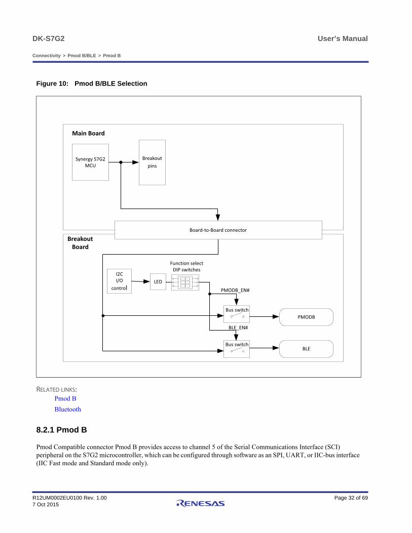
8.2 Pmod B/BLE
The Bluetooth Low Energy (BLE) device and Pmod Compatible connector Pmod B both use the Serial Communication Interface (SCI) channel 5 of the S7G2 microcontroller. Only the BLE device or Pmod B may be enabled at any time. To connect or disconnect the BLE or Pmod B, use DIP switch S101.
Figure 10 shows the connectivity.
Table 5: Pmod D connector (J100)
PMODD connector (Breakout Board) S7G2 microcontroller
Pin Description Pin Function name
1 SCI CTS P307 (P3_7) CTS6
2 SCI transmit P305 (P3_5) TXD6
3 SCI receive P304 (P3_4) RXD6
4 SCI serial clock P306 (P3_6) SCK6
5, 11 GND - -
6, 12 +3V3 or +5V depending on the setting of J103
- -
7 IRQ P009 (P0_9) -
8 GPIO P603 (P6_3) -
9 GPIO P604 (P6_4) -
10 GPIO P605 (P6_5) -
DK-S7G2 User’s Manual
Connectivity > Pmod B/BLE > Pmod B
R12UM0002EU0100 Rev. 1.00 Page 32 of 697 Oct 2015
Figure 10: Pmod B/BLE Selection
RELATED LINKS:Pmod B
Bluetooth
8.2.1 Pmod B
Pmod Compatible connector Pmod B provides access to channel 5 of the Serial Communications Interface (SCI) peripheral on the S7G2 microcontroller, which can be configured through software as an SPI, UART, or IIC-bus interface (IIC Fast mode and Standard mode only).

DK-S7G2 User’s Manual
Connectivity > Pmod B/BLE > Bluetooth
R12UM0002EU0100 Rev. 1.00 Page 33 of 697 Oct 2015
The Pmod B connector and the BLE device connect to the same pins on the S7G2 microcontroller. To use Pmod B, set the DIP switches to disable the BLE device connections and enable the Pmod B connections:
1) Set DIP switch 7 on S101 (BLE) to OFF.
2) Enable Pmod B by one of the following methods:
• Set DIP switch 6 (PMODB) on S101 to ON.
• If DIP switch 6 on S101 is in the OFF position, PMODB can be enabled under software control through the IIC-controlled I/O Expander U119.
RELATED LINKS:Configuration
Breakout Board Components
8.2.2 Bluetooth
The BLE device is connected to channel 5 of the Serial Communications Interface (SCI) peripheral on the S7G2 microcontroller, which must be configured through software as an SPI interface when used for the BLE device.
Table 6: Pmod B connector (J106)
PMODB connector (Breakout Board) S7G2 microcontroller
Pin Description Pin Function name
1 SCI CTS P507 (P5_7) CTS5
2 SCI transmit P509 (P5_9) TXD5
3 SCI receive P510 (P5_10) RXD5
4 SCI serial clock P508 (P5_8) SCK5
5, 11 GND - -
6, 12 +3V3 or +5V depending on the setting of J109
- -
7 IRQ P005 (P0_5) -
8 GPIO PA05 (PA_5) -
9 GPIO PA06 (PA_6) -
10 GPIO PA07 (PA_7) -

DK-S7G2 User’s Manual
Connectivity > Ethernet 1/camera > Bluetooth
R12UM0002EU0100 Rev. 1.00 Page 34 of 697 Oct 2015
The Pmod B connector and the BLE device connect to the same pins on the S7G2 microcontroller. To use the BLE device, set the DIP switches to disable the Pmod B connections and enable the BLE device connections:
1) Set DIP switch 6 (PMODB) on S101 to OFF.
2) Enable the BLE Device by one of the following methods:
• Set DIP switch 7 (BLE) on S101 to ON.
• If DIP switch 7 on S101 is in the OFF position, BLE can be enabled under software control through the IIC-controlled I/O Expander U119.
RELATED LINKS:Configuration
Breakout Board Components
8.3 Ethernet 1/camera
The Ethernet connector ENET1 on the Main Board and the camera interface on the Breakout Board share pins of the S7G2 microcontroller.
Table 7: BLE Interface (RF1)
BLE Device (Main Board) S7G2 microcontroller
Pin Description Pin Function name
BLE_CS# SPI mode Chip Select P507 (P5_7) CTS5
BLE_MISO SPI Master In Slave Out P510 (P5_10) RXD5
BLE_MOSI SPI Master Out Slave In P507 (P5_9) TXD5
BLE_SCK SPI Serial Clock P508 (P5_8) SCK5
BLE_IRQ# BLE Interrupt P005 (P0_5) IRQ10-DS
BLE_RESET BLE Reset PA05 (PA_5) GTIOC11A_B

DK-S7G2 User’s Manual
Connectivity > Ethernet 1/camera > Ethernet 1
R12UM0002EU0100 Rev. 1.00 Page 35 of 697 Oct 2015
Figure 11: Ethernet 1/camera interface selection
RELATED LINKS:Ethernet 1
Camera interface
8.3.1 Ethernet 1
The Ethernet 1 PHY is connected to the Ethernet MAC Controller (ETHERC) channel 1 on the S7G2 microcontroller. The Ethernet signals of the Ethernet 1 PHY on the Main Board are shared with the camera interface signals on the

DK-S7G2 User’s Manual
Connectivity > Ethernet 1/camera > Camera interface
R12UM0002EU0100 Rev. 1.00 Page 36 of 697 Oct 2015
Breakout Board. To use the Ethernet 1 connector, set the DIP switches to disable the camera connections and enable the Ethernet 1 connections:
1) Set DIP switch 8 on S101 (CAM) to OFF.
2) Enable the Ethernet connector by one of the following methods:
• Set DIP switch 3 (ENET1) on S5 to ON.
• If DIP switch 3 on S5 is in the OFF position, all Ethernet signals to the Ethernet PHY can be enabled under software control through the IIC-controlled I/O Expander U22.
To measure the propagation delay of the Ethernet signals across buffer U18, use test point TP5 located on the PHY side of U18. The signal delay can be measured between breakout pin P0_2 on breakout pin connector J9 and TP5.
RELATED LINKS:Configuration
Main Board Components
8.3.2 Camera interface
The camera interface is connected to Parallel Data Capture (PDC) peripheral on the S7G2 microcontroller. The IIC channel 7 controls the camera settings as well as image acquisition and image quality. The camera interface signals are shared with the Ethernet signals of the Ethernet 1 connector on the Main Board. To use the camera interface, set the DIP switches to disable the Ethernet 1 connections and enable the camera connections:
1) Set DIP switch 3 (ENET1) on S5 to OFF.
2) Enable the camera interface by one of the following methods:
• Set DIP switch 8 (CAM) on S101 to ON.
• If DIP switch 8 on S101 is in the OFF position, all camera interface signals except the IIC-bus control signals can be enabled under software control through the IIC-controlled I/O Expander U119.
Table 8: Camera interface (J101)
Camera interface connector (Breakout Board) S7G2 microcontroller
Pin Description Pin Function name
3 PA_3/SCL7 PA03 (PA_3) SCL7
4 PA_2/SDA7 PA02 (PA_2) SDA7
5 VSYNC P512 (P5_12) VSYNC
6 HSYNC P704 (P7_4) HSYNC
7 PIXCLK P705 (P7_5) PIXCLK

DK-S7G2 User’s Manual
Connectivity > SD Card/eMMC/Ethernet 0 > Camera interface
R12UM0002EU0100 Rev. 1.00 Page 37 of 697 Oct 2015
RELATED LINKS:Configuration
Breakout Board Components
8.4 SD Card/eMMC/Ethernet 0
The following devices on the Breakout Board all share the same pins of the of the S7G2 microcontroller:
• eMMC
• SD Card
• Ethernet 0
Figure 12 shows the connectivity.
8 PCKO P511 (P5_11) PCKO
9 PXD7 P403 (P4_3) PIXD7
10 PXD6 P404 (P4_4) PIXD6
11 PXD5 P405 (P4_5) PIXD5
12 PXD4 P406 (P4_6) PIXD4
13 PXD3 P700 (P7_0) PIXD3
14 PXD2 P701 (P7_1) PIXD2
15 PXD1 P702 (P7_2) PIXD1
16 PXD0 P703 (P7_3) PIXD0
17 CAM_RESET# PB06 (PB_6) GPIO
18 CAM_PWDN# PB07 (PB_7) GPIO
Table 8: Camera interface (J101) (Continued)
Camera interface connector (Breakout Board) S7G2 microcontroller
Pin Description Pin Function name

DK-S7G2 User’s Manual
Connectivity > SD Card/eMMC/Ethernet 0 > Camera interface
R12UM0002EU0100 Rev. 1.00 Page 38 of 697 Oct 2015
Figure 12: eMMC/SD Card/Ethernet 0 Selection
RELATED LINKS:SD/MMC Interface
Ethernet 0

DK-S7G2 User’s Manual
Connectivity > SD Card/eMMC/Ethernet 0 > SD/MMC Interface
R12UM0002EU0100 Rev. 1.00 Page 39 of 697 Oct 2015
8.4.1 SD/MMC Interface
The SD card interface and the MMC interface are both connected to the channel 0 of the SD/MMC controller on the S7G2 microcontroller. However, the bus and control signals to each device can be enabled separately through two DIP switches on S101 or through software.
The SD/MMC controller uses a four-bit wide data bus for the SD Card interface and an up to eight-bit wide data bus for the external memory eMMC.
CAUTION: Pin P313 (P3_13) is used for the eMMC data bus and for the LCD control signal TCON. When both the LCD and the eMMC are used with the DK-S7G2, the data bus on the eMMC is limited to the lower four bits (MMC D0 to MMC D3).
The SD/MMC signals on the Breakout Board are shared with the Ethernet 0 signals on the Breakout Board.
8.4.1.1 SD card interface
To use the SD card interface (SD100) on the DK-S7G2 Breakout Board:
1) Set DIP switch 3 (ENET0) on S101 to OFF.
2) Set DIP switch 5 (MMC) on S101 to OFF.
3) Enable the SD card interface by one of the following methods:
• Set DIP switch 4 (SD) on S101 to ON.
• If DIP switch 4 on S101 is in the OFF position, all SD card interface signals can be enabled under software control through the IIC-controlled I/O Expander U119.
8.4.1.2 eMMC interface
To use the eMMC interface (U110) on the DK-S7G2 Breakout Board:
1) Set DIP switch 3 (ENET0) on S101 to OFF.
2) Set DIP switch 4 (SD) on S101 to OFF.
3) Enable the eMMC interface by one of the following methods:
• Set DIP switch 5 (MMC) on S101 to ON.
• If DIP switch 5 on S101 is in the OFF position, all eMMC interface signals can be enabled under software control through the IIC-controlled I/O Expander U119.
RELATED LINKS:Configuration
Breakout Board Components

DK-S7G2 User’s Manual
Connectivity > RS-232/485 > Ethernet 0
R12UM0002EU0100 Rev. 1.00 Page 40 of 697 Oct 2015
8.4.2 Ethernet 0
The Ethernet 0 PHY (U116 on the Breakout Board) is connected to the Ethernet MAC Controller (ETHERC) channel 0 on the S7G2 microcontroller. The Ethernet signals of the Ethernet 0 PHY on the Breakout Board are shared with the eMMC and SD Card signals on the Breakout Board.
To use the Ethernet 0 PHY with connector J113 on the DK-S7G2 Breakout Board:
1) Set DIP switch 5 (MMC) on S101 to OFF.
2) Set DIP switch 4 (SD) on S101 to OFF.
3) Enable the Ethernet 0 interface by one of the following methods:
• Set DIP switch 3 (ENET0) on S101 to ON.
• If DIP switch 3 on S101 is in the OFF position, all Ethernet signals to the Ethernet PHY can be enabled under software control through the IIC-controlled I/O Expander U119.
RELATED LINKS:Configuration
Breakout Board Components
8.5 RS-232/485
The RS-232/485 signals are controlled by the RS-232/485 transceiver (U118) on the Breakout Board. The transceiver uses channel 1 of the Serial Communication Interface (SCI) on the S7G2 microcontroller, which must be configured through software as a UART interface. Two GPIO pins are used to turn the transceiver and the receive channel on and off. The transceiver signals are routed to connector J112 on the Breakout Board.
The RS-232/485 transceiver signals are not shared with other devices on the DK-S7G2.
To use the RS-232/485 transceiver on the DK-S7G2 Breakout Board, enable the RS-232/485 signal connections by one of the following methods:
• Set DIP switch 1 (RS) on S101 to ON.
• If DIP switch 1 on S101 is in the OFF position, the RS-232/485 signal connections can be enabled under software control through the IIC-controlled I/O Expander U119.
Table 9: RS-232/485device (U118)
RS-232/485 device (Breakout Board) S7G2 microcontroller
Pin Description Pin Function name
RS_RX UART Receive P708 (P7_8) RXD1
RS_DEN RS DEN P914 (P9_14) GPIO

DK-S7G2 User’s Manual
Connectivity > CAN > Ethernet 0
R12UM0002EU0100 Rev. 1.00 Page 41 of 697 Oct 2015
RELATED LINKS:Configuration
Breakout Board Components
8.6 CAN
The CAN signals are controlled by the CAN transceiver (U112) on the Breakout Board. The transceiver uses channel 0 of the CAN Controller on the S7G2 microcontroller. The transceiver signals are routed to connector J112 on the Breakout Board.
The CAN Transceiver signals are not shared with other devices on the DK-S7G2.
To use the CAN transceiver on the DK-S7G2 Breakout Board, enable the CAN Transceiver signal connections by one of the following methods:
• Set DIP switch 2 (CAN) on S101 to ON.
• If DIP switch 2 on S101 is in the OFF position, the CAN transceiver can be enabled under software control through the IIC-controlled I/O Expander U119.
RELATED LINKS:Configuration
Breakout Board Components
RS_TX UART Transmit P709 (P7_9) TXD1
RS_ON RS ON P915 (P9_15) GPIO
Table 10: CAN transceiver (U112)
CAN transceiver (Breakout Board) S7G2 microcontroller
Pin Description Pin Function name
CAN_TX CAN Transmit P811 (P8_11) CTX0
CAN_RX CAN Receive P812 (P8_12) CRX0
Table 9: RS-232/485device (U118) (Continued)
RS-232/485 device (Breakout Board) S7G2 microcontroller
Pin Description Pin Function name

DK-S7G2 User’s Manual
Connectivity > Pmod A > Ethernet 0
R12UM0002EU0100 Rev. 1.00 Page 42 of 697 Oct 2015
8.7 Pmod A
Pmod Compatible connector Pmod A provides access to channel 8 of the Serial Communications Interface (SCI) peripheral on the S7G2 microcontroller, which can be configured through software as an SPI, UART, or IIC-bus interface (IIC Fast mode and Standard mode only).
The Pmod A signals are not shared with other devices on the DK-S7G2.
To use the 12-pin Pmod A connector (PMODA) on the DK-S7G2 Main Board, enable the Pmod A signal connections by one of the following methods:
• Set DIP switch 4 (PMOD) on S5 to ON.
• If DIP switch 4 on S5 is in the OFF position, PMODA can be enabled under software control through the IIC-controlled I/O Expander (U22).
RELATED LINKS:Configuration
Main Board Components
Table 11: Pmod A connector (J5)
PMODA connector (Main Board) S7G2 microcontroller
Pin Description Pin Function name
1 SCI CTS PB02 (PB_2) CTS8
2 SCI transmit PB04 (PB_4) TXD8
3 SCI receive PB05 (PB_5) RXD8
4 SCI serial clock PB03 (PB_3) SCK8
5, 11 GND - -
6, 12 +3V3 or +5V depending on the setting of J6
- -
7 IRQ P004 (P0_4) -
8 GPIO P911 (P9_11) -
9 GPIO P912 (P9_12) -
10 GPIO P913 (P9_13) -

DK-S7G2 User’s Manual
Connectivity > QSPI flash > Ethernet 0
R12UM0002EU0100 Rev. 1.00 Page 43 of 697 Oct 2015
8.8 QSPI flash
The QSPI flash signals are not shared with other devices on the DK-S7G2.
To use the on-board QSPI flash on the DK-S7G2 Main Board, enable the QSPI flash signal connections by one of the following methods:
• Set DIP switch 2 (QSPI) on S5 to ON.
• If DIP switch 2 on S5 is in the OFF position, the QSPI flash can be enabled under software control through the IIC-controlled I/O Expander (U22).
To measure the propagation delay of the QSPI flash signals across buffer U15 on the DK-S7G2 Main Board, use test point TP4, located on the QSPI side of buffer U15. The signal delay can be measured between breakout pin P5_1 on the breakout pin connector J10 and TP4.
RELATED LINKS:Configuration
Main Board Components
8.9 Push buttons
The Main Board features three push buttons, which are connected to the external interrupt inputs of the S7G2 microcontroller. The push button connections are not shared with other devices on the DK-S7G2.
To use the push buttons on the DK-S7G2 Main Board, enable the push button signal connections by one of the following methods:
• Set DIP switch 5 (PBs) on S5 to ON.
Table 12: QSPI flash
QSPI flash (Main Board) S7G2 microcontroller
Pin Description Pin Function name
QSPI CS# - P501 (P5_1) QSSL
QSPI CLK - P500 (P5_0) QSPCLK
QSPI DQ0 - P502 (P5_2) QIO0
QSPI DQ1 - P503 (P5_3) QIO1
QSPI DQ2 - P504 (P5_4) QIO2
QSPI DQ3 - P505 (P5_5) QIO3

DK-S7G2 User’s Manual
Connectivity > User LEDs > Ethernet 0
R12UM0002EU0100 Rev. 1.00 Page 44 of 697 Oct 2015
• If DIP switch 5 on S5 is in the OFF position, the push buttons can be enabled under software control through the IIC-controlled I/O Expander (U22).
RELATED LINKS:Configuration
8.10 User LEDs
The Main Board features two LEDs, which can be controlled by the application through the GPIO pins of the S7G2 microcontroller. Each LED supports two colors, red and green, which can be individually turned on or off through the corresponding GPIO pins.
The user LED signal connections are not shared with other devices on the DK-S7G2.
RELATED LINKS:Configuration
Table 13: Push Buttons (S1 to S3)
Push Buttons (Main Board) S7G2 microcontroller
Pin Description Pin Function name
S1 IRQ11 P006 (P0_6) IRQ11
S2 IRQ14 P010 (P0_10) IRQ14
S3 IRQ15 P011 (P0_11) IRQ15
Table 14: LED1 and LED2
User LED (Main Board) S7G2 microcontroller
Pin Description Pin Function name
LED1 Green, LED2_G P807 (P8_7) GPIO
LED1 Red, LED2_R P808 (P8_8) GPIO
LED2 Green, LED3_G P809 (P8_9) GPIO
LED2 Red, LED3_R P810 (P8_10) GPIO

DK-S7G2 User’s Manual
Connectivity > JTAG > Ethernet 0
R12UM0002EU0100 Rev. 1.00 Page 45 of 697 Oct 2015
8.11 JTAG
The JTAG signals can be used through the J-Link OB USB port (J17), directly through the JTAG connector J16, or through the SEGGER J-Link OB connector J15. The SEGGER J-Link OB connector and the J-Link OB USB port are connected to the RX621 microcontroller (U24).
The JTAG signal connections are not shared with other devices on the DK-S7G2.
To use the JTAG signals on the DK-S7G2 Main Board, enable the JTAG signal connections by one of the following methods:
• Set DIP switch 6 (JTAG) on S5 to ON.
• If DIP switch 6 on S5 is in the OFF position, the JTAG signals can be enabled under software control through the IIC-controlled I/O Expander (U22).
NOTE: The JTAG Trace port signals are not affected by DIP switch 6.
RELATED LINKS:Configuration
Main Board Components
Table 15: JTAG
JTAG (Main Board) S7G2 microcontroller
Pin Description Pin Function name
TMS/SWDIO - P108 (P1_8) TMS/SWDIO
TCK/SWCLK - P300 (P3_0) TCK/SWCLK
TDO - P109 (P1_9) TDO
TDI - P110 (P1_10) TDI
RESET# - RESET#
TCLK - PA12 (PA_12) TCLK
TDATA0 - PA13 (PA_13) TDATA0
TDATA1 - PA14 (PA_14) TDATA1
TDATA2 - PA15 (PA_15) TDATA2
TDATA3 - P813 (P8_13) TDATA3

DK-S7G2 User’s Manual
e2 studio Support > Project configuration > Ethernet 0
R12UM0002EU0100 Rev. 1.00 Page 46 of 697 Oct 2015
Chapter 9 e2 studio Support
The DK-S7G2 is fully supported by the e2 studio ISDE and the Renesas Synergy Software Package (SSP). When you download the SSP, the DK-S7G2 related configuration files are included in the pack.
9.1 Project configuration
During the Synergy Project configuration steps in the e2 studio ISDE, specify DK-S7G2 in the Device Selection box of the Synergy Configuration view. This selection enables several project templates for the DK-S7G2:
• Project template for developing RTOS-independent applications
• Project template for developing ThreadX-based applications
• Project template for a simple demonstration application (Blinky)
• Project template for a thermostat reference application
Figure 13: e2 studio ISDE DK-S7G2 Project templates

DK-S7G2 User’s Manual
e2 studio Support > Board Support Package (BSP) configuration > Ethernet 0
R12UM0002EU0100 Rev. 1.00 Page 47 of 697 Oct 2015
9.2 Board Support Package (BSP) configuration
The DK-S7G2 BSP is included in the Renesas Synergy Software Package (SSP) and contains all board specific configuration files to set up the S7G2 microcontroller’s ROM registers, clocks, interrupts, and the Event Link Controller (ELC) events. The initial pin configuration for this board is also included in the BSP. The BSP and its configuration files enable the S7G2 microcontroller on this board to boot up from reset to the start of code execution in the user’s application main.c file.
The initial BSP settings for the DK-S7G2 are displayed in the e2 studio ISDE in the Synergy Configuration view under the BSP tab in the Properties window.
Figure 14: DK-S7G2 BSP Settings
You can edit any of the BSP properties in the Properties window to optimize memory use and code generation for your application. However, be careful when changing the properties as incorrect settings may prevent access to required memory areas or to the entire chip.
The BSP configuration parameters are included in the file ssp_cfg\bsp\bsp_cfg.h in the SSP.
IMPORTANT: The SSP User’s Manual includes a detailed description of the BSP Architecture and the BSP configuration parameters.

DK-S7G2 User’s Manual
e2 studio Support > Clock configuration > Ethernet 0
R12UM0002EU0100 Rev. 1.00 Page 48 of 697 Oct 2015
9.3 Clock configuration
The BSP determines the initial clock configuration of the S7G2 microcontroller for the particular board on start-up. You can see and edit the clock configuration in the Clocks window of the Synergy Configuration view.
Figure 15: DK-S7G2 Clock settings
The BSP clock configuration parameters are included in the file ssp_cfg\bsp\bsp_clock_cfg.h in the SSP.
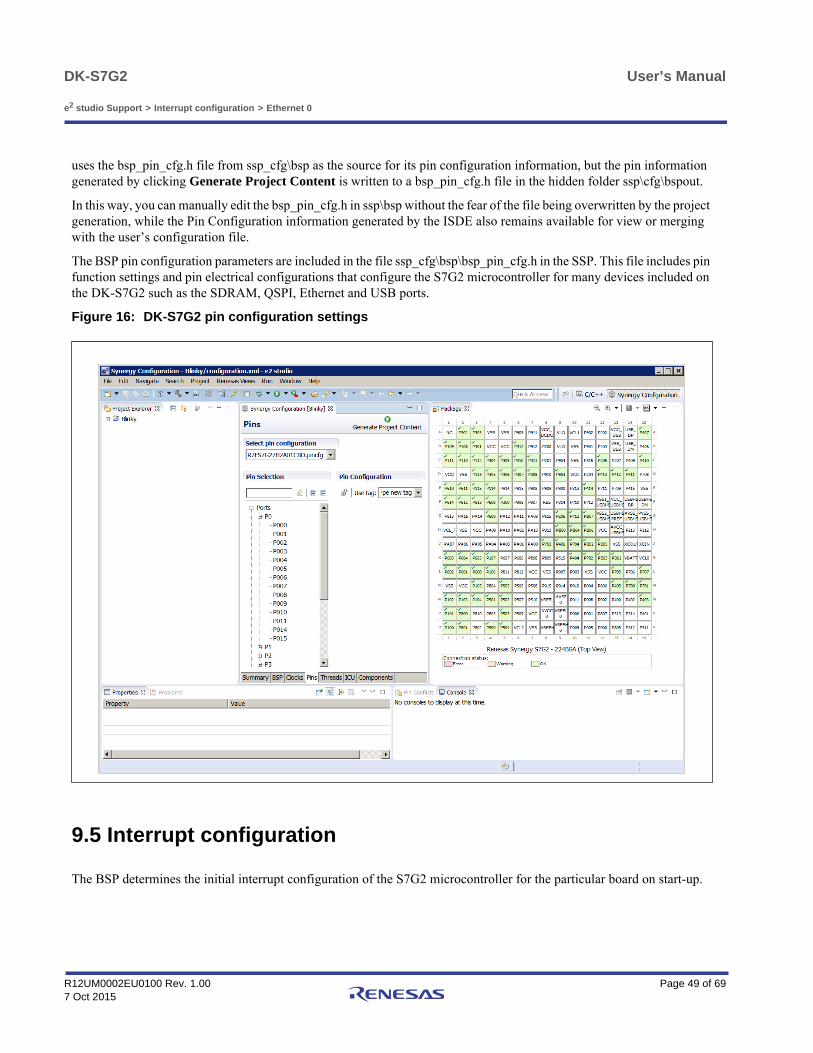
9.4 Pin configuration
The BSP determines the initial pin configuration of the S7G2 microcontroller for the particular board on start-up.
During start-up, and before main() is executed, the BSP iterates over this array and initializes the microcontroller's port pins based on the settings in the array. Initially, before any pin configuration by the user, the Pins tab displays the initial reference configuration defined for the selected board type. Once the user modifies the pin configuration and clicks Generate Project Content, a new bsp_pin_cfg.h file is generated containing the new pin configuration. The BSP always
DK-S7G2 User’s Manual
e2 studio Support > Interrupt configuration > Ethernet 0
R12UM0002EU0100 Rev. 1.00 Page 49 of 697 Oct 2015
uses the bsp_pin_cfg.h file from ssp_cfg\bsp as the source for its pin configuration information, but the pin information generated by clicking Generate Project Content is written to a bsp_pin_cfg.h file in the hidden folder ssp\cfg\bspout.
In this way, you can manually edit the bsp_pin_cfg.h in ssp\bsp without the fear of the file being overwritten by the project generation, while the Pin Configuration information generated by the ISDE also remains available for view or merging with the user’s configuration file.
The BSP pin configuration parameters are included in the file ssp_cfg\bsp\bsp_pin_cfg.h in the SSP. This file includes pin function settings and pin electrical configurations that configure the S7G2 microcontroller for many devices included on the DK-S7G2 such as the SDRAM, QSPI, Ethernet and USB ports.
Figure 16: DK-S7G2 pin configuration settings
9.5 Interrupt configuration
The BSP determines the initial interrupt configuration of the S7G2 microcontroller for the particular board on start-up.

DK-S7G2 User’s Manual
e2 studio Support > QSPI set-up > Ethernet 0
R12UM0002EU0100 Rev. 1.00 Page 50 of 697 Oct 2015
Figure 17: DK-S7G2 Interrupt settings
The BSP interrupt configuration parameters are included in the file ssp_cfg\bsp\bsp_irq_cfg.h in the SSP. This file includes all interrupts usable on the DK-S7G2. All interrupts are disabled by default. This file is overwritten when you change the project configuration by pressing the Generate Project Configuration Button.
9.6 QSPI set-up
The QSPI parameters are configured as part of the BSP for the particular QSPI device mounted on the Main Board. The configuration settings are included in the following files in the SSP:
• bsp_qspi.c
• bsp_qspi.h
See 32-MB QSPI serial flash for the QSPI hardware specifications.

DK-S7G2 User’s Manual
e2 studio Support > SDRAM set-up > Ethernet 0
R12UM0002EU0100 Rev. 1.00 Page 51 of 697 Oct 2015
Figure 18: DK-S7G2 BSP Settings for QSPI
NOTE: The QSPI configuration files are not available for editing through an e2 studio property window.
9.7 SDRAM set-up
The SDRAM parameters are configured as part of the BSP for the particular SDRAM device mounted on the Main Board. The configuration settings are defined in the following files in the SSP in the same way as for the QSPI describe above:
• bsp_sdram.c
• bsp_sdram.h
See SDRAM for the SDRAM hardware specifications.
NOTE: The SDRAM configuration files are not available for editing through an e2 studio property window.

DK-S7G2 User’s Manual
e2 studio Support > User LED set-up > Application notes
R12UM0002EU0100 Rev. 1.00 Page 52 of 697 Oct 2015
9.8 User LED set-up
The GPIO pins used for the user-programmable LEDs are configured as part of the BSP. The configuration settings defined in the following files in the SSP:
• bsp_leds.c
• bsp_leds.h
9.9 Software features
Demonstration software programs are available as downloads from the Renesas Synergy Gallery in the form of a CMSIS-Pack that can be imported to the e2 studio Integrated System Development Environment (ISDE) to build and run on the DK-S7G2.
9.9.1 Application notes
Application notes and demonstration applications are available in the Demos and Applications tab of the Renesas Synergy website at https://synergygallery.renesas.com/ssp. Examples of the categories we are developing are:
• Wired connectivity (CAN, RS-232/485, TCP/IP, web server, networking services)
• Bluetooth connectivity (Bluetooth Classic and Bluetooth Low Energy connection to mobile devices using various profiles)
• Wi-Fi connectivity (access point enumeration, access point connection using secure protocols, TCP/IP, web server, networking services)
• Multi-media (webcam, audio playback and record, audio processing, GUIX tutorials)
• MCU performance and power measurement (thread, throughput, and I/O performance, low-power modes and power measurement)
• Security (protected memory and bus access examples, stack security examples, security protocols and services examples)
9.9.2 Suggested links
Renesas Synergy Gallery
• https://synergygallery.renesas.com
Support
• https://synergygallery.renesas.com/support
Technical Contact Details
• America: https://renesas.zendesk.com/anonymous_requests/new

DK-S7G2 User’s Manual
e2 studio Support > Software features > Suggested links
R12UM0002EU0100 Rev. 1.00 Page 53 of 697 Oct 2015
• Europe: http://www.renesas.eu/support/index.jsp
• Japan: https://synergybeta.renesas.com

DK-S7G2 User’s Manual
Appendix A > Pin connections - Main Board > Suggested links
R12UM0002EU0100 Rev. 1.00 Page 54 of 697 Oct 2015
Chapter 10 Appendix A
10.1 Pin connections - Main Board
The table Pin and board-to-board connectors on the Main Board shows the peripherals and their signals supported by the Main Board. Some peripherals such as the Ethernet 1 or the peripherals accessed through the Pmod A connector can be disabled entirely through switch S5. The corresponding pins are then available for another component on the Breakout Board or for another function as defined by the pin function multiplexing of the S7G2 microcontroller.
The microcontroller port pins with their functions selected by switch S5 are routed from the Main Board to the Breakout Board through connectors J11 to J14 on the Main Board.
All port pins regardless of their assigned function can be monitored through the breakout pin connectors J7 to J10 on the Main Board.
Table 16: Pin and board-to-board connectors on the Main Board
S7G2 Pin - available on
connectors J7 to J10aPeripheral Signal DK2M
board-to-board connection
P0_0/AN000 (P000) No connector on Main Board - J11-3
P0_1/AN001 (P001) No connector on Main Board - J11-4
P0_2/AN002 (P002) ETH1 (enable/disable switch S5) IRQ# J11-5
P0_3/PGAVSS000 (P003) No connector on Main Board - J11-6
P0_4/AN100 (P004) PMODA (SCI8) (enable/disable switch S5) IRQ# J11-7
P0_5/AN101 (P005) No connector on Main Board - J11-8
P0_6/AN102 (P006) PB (enable/disable switch S5) S1 J11-9
P0_7/PGAVSS100 (P007) No connector on Main Board - J11-10
P0_8/AN003 (P008) No connector on Main Board - J11-11
P0_9/AN004 (P009) No connector on Main Board - J11-12
P0_10/AN103 (P010) PB (enable/disable switch S5) S2 J11-15
P0_11/AN104 (P011) PB (enable/disable switch S5) S3 J11-16

DK-S7G2 User’s Manual
Appendix A > Pin connections - Main Board > Suggested links
R12UM0002EU0100 Rev. 1.00 Page 55 of 697 Oct 2015
P0_14/DA0/AN005/AN105 (P014)
No connector on Main Board - J11-17
P0_15/DA1/AN006/AN106 (P015)
No connector on Main Board - J11-18
P1_0 (P100) SDRAM (enable/disable switch S5) DQ0 J11-19
P1_1 (P101) SDRAM (enable/disable switch S5) DQ1 J11-20
P1_2 (P102) SDRAM (enable/disable switch S5) DQ2 J11-21
P1_3 (P103) SDRAM (enable/disable switch S5) DQ3 J11-22
P1_4 (P104) SDRAM (enable/disable switch S5) DQ4 J11-23
P1_5 (P105) SDRAM (enable/disable switch S5) DQ5 J11-24
P1_6 (P106) SDRAM (enable/disable switch S5) DQ6 J11-25
P1_7 (P107) SDRAM (enable/disable switch S5) DQ7 J11-26
P1_8 (P108) JTAG (enable/disable switch S5) TMS J11-27
P1_9 (P109) JTAG (enable/disable switch S5) TDO J11-28
P1_10 (P110) JTAG (enable/disable switch S5) TDI J11-29
P1_11 (P111) SDRAM (enable/disable switch S5) A5 J11-30
P1_12 (P112) SDRAM (enable/disable switch S5) A4 J11-31
P1_13 (P113) SDRAM (enable/disable switch S5) A3 J11-32
P1_14 (P114) SDRAM (enable/disable switch S5) A2 J11-35
P1_15 (P115) SDRAM (enable/disable switch S5) A1 J11-36
P2_2 (P202) No connector on Main Board - J11-37
P2_3 (P203) No connector on Main Board - J11-38
P2_4 (P204) No connector on Main Board - J11-39
Table 16: Pin and board-to-board connectors on the Main Board (Continued)
S7G2 Pin - available on
connectors J7 to J10aPeripheral Signal DK2M
board-to-board connection

DK-S7G2 User’s Manual
Appendix A > Pin connections - Main Board > Suggested links
R12UM0002EU0100 Rev. 1.00 Page 56 of 697 Oct 2015
P2_5 (P205) No connector on Main Board - J11-40
P2_6 (P206) No connector on Main Board - J11-41
P2_7 (P207) No connector on Main Board - J11-42
P3_0 (P300) JTAG (enable/disable switch S5) TCK J13-3
P3_1 (P301) SDRAM (enable/disable switch S5) A6 J13-4
P3_2 (P302) SDRAM (enable/disable switch S5) A7 J13-5
P3_3 (P303) SDRAM (enable/disable switch S5) A8 J13-6
P3_4 (P304) SDRAM (enable/disable switch S5) A9 J13-7
P3_5 (P305) SDRAM (enable/disable switch S5) A10 J13-8
P3_6 (P306) SDRAM (enable/disable switch S5) A11 J13-9
P3_7 (P307) SDRAM (enable/disable switch S5) A12 J13-10
P3_8 (P308) SDRAM (enable/disable switch S5) A13 J13-11
P3_9 (P309) SDRAM (enable/disable switch S5) A14 J13-12
P3_10 (P310) SDRAM (enable/disable switch S5) A15 J13-15
P3_11 pr P311) SDRAM (enable/disable switch S5) RAS# J13-16
P3_12 (P312) SDRAM (enable/disable switch S5) CAS# J13-17
P3_13 (P313) No connector on Main Board - J13-18
P3_14 (P314) No connector on Main Board - J13-19
P3_15 (P315) No connector on Main Board - J13-20
P4_0 (P400) No connector on Main Board - J13-21
P4_1 (P401) No connector on Main Board - J13-22
P4_2 (P402) No connector on Main Board - J13-23
Table 16: Pin and board-to-board connectors on the Main Board (Continued)
S7G2 Pin - available on
connectors J7 to J10aPeripheral Signal DK2M
board-to-board connection

DK-S7G2 User’s Manual
Appendix A > Pin connections - Main Board > Suggested links
R12UM0002EU0100 Rev. 1.00 Page 57 of 697 Oct 2015
P4_3 (P403) ETH1 (enable/disable switch S5) MDC J13-24
P4_4 (P404) ETH1 (enable/disable switch S5) MDIO J13-25
P4_5 (P405) ETH1 (enable/disable switch S5) TXEN J13-26
P4_6 (P406) ETH1 (enable/disable switch S5) TXD1 J13-27
P4_7 (P407) USBFS VBUS J13-28
P4_8 (P408) No connector on Main Board - J13-29
P4_9 (P409) No connector on Main Board - J13-30
P4_10 (P410) No connector on Main Board - J13-31
P4_11 (P411) No connector on Main Board - J13-32
P4_12 (P412) No connector on Main Board - J13-35
P4_13 (P413) No connector on Main Board - J13-36
P4_14 (P414) No connector on Main Board - J13-37
P4_15 (P415) No connector on Main Board - J13-38
P5_0/AN016 (P500) QSPI (enable/disable switch S5) CLK J13-39
P5_1/AN116 (P501) QSPI (enable/disable switch S5) CS# J13-40
P5_2/AN017 (P502) QSPI (enable/disable switch S5) DQ0 J13-41
P5_3/AN117 (P503) QSPI (enable/disable switch S5) DQ1 J13-42
P5_4/AN018 (P504) QSPI (enable/disable switch S5) DQ2 J13-43
P5_5/AN118 (P505) QSPI (enable/disable switch S5) DQ3 J13-44
P5_6/AN019 (P506) No connector on Main Board - J13-45
P5_7/AN119 (P507) No connector on Main Board - J13-46
P5_8/AN020 (P508) No connector on Main Board - J13-49
Table 16: Pin and board-to-board connectors on the Main Board (Continued)
S7G2 Pin - available on
connectors J7 to J10aPeripheral Signal DK2M
board-to-board connection

DK-S7G2 User’s Manual
Appendix A > Pin connections - Main Board > Suggested links
R12UM0002EU0100 Rev. 1.00 Page 58 of 697 Oct 2015
P5_9/AN120 (P509) No connector on Main Board - J13-50
P5_10/AN021 (P510) No connector on Main Board - J13-51
P5_11 (P511) No connector on Main Board - J13-52
P5_12 (P512) No connector on Main Board - J13-53
P5_13 (P513) No connector on Main Board - J13-54
P5_14 (P514) No connector on Main Board - J13-55
P5_15 (P515) No connector on Main Board - J13-56
P6_0 (P600) No connector on Main Board - J12-3
P6_1 (P601) SDRAM (enable/disable switch S5) LDQM J12-4
P6_2 (P602) SDRAM (enable/disable switch S5) CLK J12-5
P6_3 (P603) SDRAM (enable/disable switch S5) DQ13 J12-6
P6_4 (P604) SDRAM (enable/disable switch S5) DQ12 J12-7
P6_5 (P605) SDRAM (enable/disable switch S5) DQ11 J12-8
P6_6 (P606) No connector on Main Board - J12-9
P6_7 (P607) No connector on Main Board - J12-10
P6_8 (P608) SDRAM (enable/disable switch S5) UDQM J12-11
P6_9 (P609) SDRAM (enable/disable switch S5) CKE J12-12
P6_10 (P610) SDRAM (enable/disable switch S5) WE# J12-15
P6_11 (P611) SDRAM (enable/disable switch S5) CS# J12-16
P6_12 (P612) SDRAM (enable/disable switch S5) DQ8 J12-17
P6_13 (P613) SDRAM (enable/disable switch S5) DQ9 J12-18
P6_14 (P614) SDRAM (enable/disable switch S5) DQ10 J12-19
Table 16: Pin and board-to-board connectors on the Main Board (Continued)
S7G2 Pin - available on
connectors J7 to J10aPeripheral Signal DK2M
board-to-board connection

DK-S7G2 User’s Manual
Appendix A > Pin connections - Main Board > Suggested links
R12UM0002EU0100 Rev. 1.00 Page 59 of 697 Oct 2015
P6_15 (P615) No connector on Main Board - J12-20
P7_0 (P700) ETH1 (enable/disable switch S5) TXD0 J12-21
P7_1 (P701) ETH1 (enable/disable switch S5) REFCLK J12-22
P7_2 (P702) ETH1 (enable/disable switch S5) RXD0 J12-23
P7_3 (P703) ETH1 (enable/disable switch S5) RXD1 J12-24
P7_4 (P704) ETH1 (enable/disable switch S5) RXER J12-25
P7_5 (P705) ETH1 (enable/disable switch S5) CRS DV J12-26
P7_6 (P706) ETH1 (enable/disable switch S5) RES# J12-27
P7_7 (P707) USBHS HS-OC -
P7_8 (P708) No connector on Main Board - J12-29
P7_9 (P709) No connector on Main Board - J12-28
P7_10 (P710) No connector on Main Board - J12-31
P7_11 (P711) No connector on Main Board - J12-30
P7_12 (P712) No connector on Main Board - J12-35
P7_13 (P713) No connector on Main Board - J12-36
P8_0 (P800) SDRAM (enable/disable switch S5) DQ14 J12-37
P8_1 (P801) SDRAM (enable/disable switch S5) DQ15 J12-38
P8_2 (P802) No connector on Main Board - J12-39
P8_3 (P803) No connector on Main Board - J12-40
P8_4 (P804) No connector on Main Board - J12-41
P8_5 (P805) No connector on Main Board - J12-42
P8_6 (P806) No connector on Main Board - J12-43
Table 16: Pin and board-to-board connectors on the Main Board (Continued)
S7G2 Pin - available on
connectors J7 to J10aPeripheral Signal DK2M
board-to-board connection

DK-S7G2 User’s Manual
Appendix A > Pin connections - Main Board > Suggested links
R12UM0002EU0100 Rev. 1.00 Page 60 of 697 Oct 2015
P8_7 (P807) User LED LED1G J12-44
P8_8 (P808) User LED LED1R J12-45
P8_9 (P809) User LED LED2G J12-46
P8_10 (P810) User LED LED2R J12-49
P8_11 (P811) No connector on Main Board - J12-50
P8_12 (P812) No connector on Main Board - J12-51
P8_13 (P813) JTAG (enable/disable switch S5) TDATA3 J12-52
P9_0 (P900) No connector on Main Board - J14-3
P9_1 (P901) No connector on Main Board - J14-4
P9_2 (P902) No connector on Main Board - J14-5
P9_3 (P903) No connector on Main Board - J14-6
P9_4 (P904) No connector on Main Board - J14-7
P9_5 (P905) No connector on Main Board - J14-8
P9_6 (P906) No connector on Main Board - J14-9
P9_7 (P907) No connector on Main Board - J14-10
P9_8 (P908) No connector on Main Board - J14-11
P9_9 (P909) No connector on Main Board - J14-12
P9_10 (P910) No connector on Main Board - J14-15
P9_11 (P911) PMODA (SCI8) (enable/disable switch S5) GPIO J14-16
P9_12 (P912) PMODA (SCI8) (enable/disable switch S5) GPIO J14-17
P9_13 (P913) PMODA (SCI8) (enable/disable switch S5) GPIO J14-18
P9_14 (P914) No connector on Main Board - J14-19
Table 16: Pin and board-to-board connectors on the Main Board (Continued)
S7G2 Pin - available on
connectors J7 to J10aPeripheral Signal DK2M
board-to-board connection

DK-S7G2 User’s Manual
Appendix A > Pin connections - Main Board > Suggested links
R12UM0002EU0100 Rev. 1.00 Page 61 of 697 Oct 2015
P9_15 (P915) No connector on Main Board - J14-20
PB_0 (PB00) USBHS VBUS_EN -
PB_2 (PB02) PMODA (SCI8) (enable/disable switch S5) CTS J14-39
PB_3 (PB03) PMODA (SCI8) (enable/disable switch S5) SCK J14-42
PB_4 (PB04) PMODA (SCI8) (enable/disable switch S5) TXD J14-41
PB_5 (PB05) PMODA (SCI8) (enable/disable switch S5) RXD J14-44
PA_0 (PA00) No connector on Main Board - J14-21
PA_1 (PA01) No connector on Main Board - J14-22
PA_2 (PA02) IIC SDA J14-23
PA_3 (PA03) IIC SCL J14-24
PA_4 (PA04) No connector on Main Board - J14-25
PA_5 (PA05) No connector on Main Board - J14-26
PA_6 (PA06) No connector on Main Board - J14-27
PA_7 (PA07) No connector on Main Board - J14-28
PA_8 (PA08) No connector on Main Board - J14-29
PA_9 (PA09) No connector on Main Board - J14-30
PA_10 (PA10) No connector on Main Board - J14-31
PA_11 (PA11) No connector on Main Board - J14-32
PA_12 (PA12) JTAG (enable/disable switch S5) TCLK J14-35
PA_13 (PA13) JTAG (enable/disable switch S5) TDATA0 J14-36
PA_14 (PA14) JTAG (enable/disable switch S5) TDATA1 J14-37
PA_15 (PA15) JTAG (enable/disable switch S5) TDATA2 J14-38
Table 16: Pin and board-to-board connectors on the Main Board (Continued)
S7G2 Pin - available on
connectors J7 to J10aPeripheral Signal DK2M
board-to-board connection

DK-S7G2 User’s Manual
Appendix A > Pin connections - Breakout Board > Suggested links
R12UM0002EU0100 Rev. 1.00 Page 62 of 697 Oct 2015
10.2 Pin connections - Breakout Board
The table Pin connectors on the Breakout Board shows the additional peripherals and connectors on the DK-S7G2 Breakout Board. The Breakout Board has one switch (S101) to enable/disable selected peripherals.
ATTENTION: Because port pins can host signals from multiple peripherals, certain settings of switches S5 on the Main Board and S101 are mutually exclusive. See tables Interfaces on the main board and Interfaces on the breakout board.
Any port pin can be probed on the Main Board through connectors J7 to J10.
PB_1 (PB01) No connector on Main Board - J14-40
PB_6 (PB06) No connector on Main Board - J14-43
PB_7 (PB07) No connector on Main Board - J14-46
XCIN SUBOSC XCIN -
XCOUT XCOUT -
RES# RESET RES# -
USBHS_RREF USBHS RREF -
USBHS_DM USBHS HS-DM -
USBHS_DP USBHS HS-DP -
USB_DM USBFS FS-DM -
USB_DP USBFS FS-DP -
a. The first pin notation refers to the schematics. The second pin notation refers to the hardware user’s manual.
Table 16: Pin and board-to-board connectors on the Main Board (Continued)
S7G2 Pin - available on
connectors J7 to J10aPeripheral Signal DK2M
board-to-board connection

DK-S7G2 User’s Manual
Appendix A > Pin connections - Breakout Board > Suggested links
R12UM0002EU0100 Rev. 1.00 Page 63 of 697 Oct 2015
Table 17: Pin connectors on the Breakout Board
Peripheral Signal Pin namea
ETH0 (enable/disable switch S101); only enable one of Ethernet 0, SD, eMMC
MDC P4_1 (P401)
MDIO P4_2 (P402)
IRQ# P0_15/DA1/AN006/AN106 (P015)
TXEN P4_15 (P415)
TXD1 P4_14 (P414)
TXD0 P4_13 (P413)
REFCLK P4_12 (P412)
RXD0 P4_11 (P411)
RXD1 P4_10 (P410)
RXER P4_9 (P409)
CRS DV P4_8 (P408)
RES# P9_3 (P903)
IRQ# P0_15/DA1/AN006/AN106 (P015)
SD (enable/disable switch S101); only enable one of Ethernet 0, SD, eMMC.
WP P4_14 (P414)
CLK P4_13 (P413)
CMD P4_12 (P412)
D0 P4_11 (P411)
D1 P4_10 (P410)
D2 P2_6 (P206)
D3 P2_5 (P205)
CD P9_3 (P903)

DK-S7G2 User’s Manual
Appendix A > Pin connections - Breakout Board > Suggested links
R12UM0002EU0100 Rev. 1.00 Page 64 of 697 Oct 2015
eMMC (enable/disable switch S101); only enable one of Ethernet 0, SD, eMMC
WP P4_14 (P414)
CLK P4_13 (P413)
CMD P4_12 (P412)
D0 P4_11 (P411)
D1 P4_10 (P410)
RES# P2_7 (P207)
D2 P2_6 (P206)
D3 P2_5 (P205)
PMODB (SCI5) (enable/disable switch S101) GPIO PA_7 (PA07)
GPIO PA_6 (PA06)
GPIO PA_5 (PA05)
CTS P5_7/AN119 (P507)
SCK P5_8/AN020 (P508)
TXD P5_9/AN120 (P509)
RXD P5_10/AN021 (P510)
IRQ# P0_5/AN101 (P005)
Table 17: Pin connectors on the Breakout Board (Continued)
Peripheral Signal Pin namea

DK-S7G2 User’s Manual
Appendix A > Pin connections - Breakout Board > Suggested links
R12UM0002EU0100 Rev. 1.00 Page 65 of 697 Oct 2015
PMODC (SCI0) (enable/disable switch S5) GPIO P6_2 (P603)
GPIO P6_1 (P601)
GPIO P6_0 (P600)
CTS P1_3 (P103)
SCK P1_2 (P102)
TXD P1_1 (P101)
RXD P1_0 (P100)
IRQ# P0_8/AN003 (P008)
PMODD (SCI6) (enable/disable switch S5) CTS P3_7 (P307)
SCK P3_6 (P306)
TXD P3_5 (P305)
RXD P3_4 (P304)
GPIO P6_5 (P605)
IRQ# P0_9/AN004 (P009)
GPIO P6_4 (P604)
GPIO P6_3 (P603)
Table 17: Pin connectors on the Breakout Board (Continued)
Peripheral Signal Pin namea

DK-S7G2 User’s Manual
Appendix A > Pin connections - Breakout Board > Suggested links
R12UM0002EU0100 Rev. 1.00 Page 66 of 697 Oct 2015
Camera (enable/disable switch 101) PXD7 P4_3 (P403)
PXD6 P4_4 (P404)
PXD5 P4_5 (P405)
PXD4 P4_6 (P406)
PXD3 P7_0 (P700)
PXD2 P7_1 (P701)
PXD1 P7_2 (P702)
PXD0 P7_3 (P703)
HSYNC P7_4 (P704)
PIXCLK P7_5 (P705)
RES# PB_6 (PB06)
PWDN# PB_7 (PB07)
VSYNC P5_12 (P512)
PCKO P5_11 (P511)
Table 17: Pin connectors on the Breakout Board (Continued)
Peripheral Signal Pin namea

DK-S7G2 User’s Manual
Appendix A > Pin connections - Breakout Board > Suggested links
R12UM0002EU0100 Rev. 1.00 Page 67 of 697 Oct 2015
LCD RES# P7_13 (P713)
BLEN P7_12 (P712)
TOUCH RES# P7_11 (P711)
ON P7_10 (P710)
VSYNC P3_13 (P313)
HSYNC P3_14 (P314)
DE P3_15 (P315)
CLK P9_0 (P900)
DATA15 P9_1 (P901)
DATA14 P9_8 (P908)
DATA13 P9_7 (P907)
DATA12 P9_6 (P906)
Table 17: Pin connectors on the Breakout Board (Continued)
Peripheral Signal Pin namea

DK-S7G2 User’s Manual
Appendix A > Pin connections - Breakout Board > Suggested links
R12UM0002EU0100 Rev. 1.00 Page 68 of 697 Oct 2015
LCD DATA11 P9_5 (P905)
DATA10 P6_15 (P615)
DATA9 PA_8 (PA08)
DATA8 PA_9 (PA09)
DATA7 PA_10 (PA10)
DATA6 PA_1 (PA01)
DATA5 PA_0 (PA00)
DATA4 P6_7 (P607)
DATA3 P6_6 (P606)
DATA2 P8_2 (P802)
DATA1 P8_3 (P803)
DATA0 P8_4 (P804)
TOUCH IRQ# P0_1/AN001 (P001)
UART (SCI1) (enable/disable switch S101; node switch S2)
TXD P7_9 (P709)
RXD P7_8 (P708)
RS ON P9_15 (P915)
RS DEN P9_14 (P914)
AUDIO EN P9_2 (P902)
DA0 P0_14/DA0/AN005/AN105 (P014)
Table 17: Pin connectors on the Breakout Board (Continued)
Peripheral Signal Pin namea

DK-S7G2 User’s Manual
Appendix A > Pin connections - Breakout Board > Suggested links
R12UM0002EU0100 Rev. 1.00 Page 69 of 697 Oct 2015
RELATED LINKS:Configuration
RF1 (SCI5) (enable/disable switch S101) RES# PA_5 (PA05)
CS# P5_7/AN119 (P507)
SCK P5_8/AN020 (P508)
MOSI P5_9/AN120 (P509)
MISO P5_10/AN021 (P510)
IRQ# P0_5/AN101 (P005)
IIC SCL PA_3 (PA03)
SDA PA_2 (PA02)
CAN (enable/disable switch S101) CTX P8_11 (P811)
RTX P8_12 (P812)
POT AN000 P0_0/AN000 (P000)
a. The first pin notation refers to the schematics. The second pin notation refers to the hardware user’s manual.
Table 17: Pin connectors on the Breakout Board (Continued)
Peripheral Signal Pin namea

Revision Record
Revision DateDescription
Page Summary
0.2 March 2015 - First preliminary version
0.2.1 April 2015 - Graphics updated; editorial changes
0.2.2 April 2015 - Graphics updated; editorial changes; software applications added
0.2.3 June 2015 - Graphics display type changed to resistive-touch WVGA
0.5 July 2015 Multiple updates throughout the document. Sections Connectivity, Configurations, e2 studio Support added. Legal disclaimer updated.
1.0 October 2015 Updated document for kit version 3

Renesas Synergy™ DK-S7G2
User’s Manual
Publication Date: Rev. 1.0 October, 2015

http://www.renesas.comRefer to "http://www.renesas.com/" for the latest and detailed information.
Renesas Electronics America Inc.2801 Scott Boulevard Santa Clara, CA 95050-2549, U.S.A.Tel: +1-408-588-6000, Fax: +1-408-588-6130
Renesas Electronics Canada Limited9251 Yonge Street, Suite 8309 Richmond Hill, Ontario Canada L4C 9T3Tel: +1-905-237-2004
Renesas Electronics Europe LimitedDukes Meadow, Millboard Road, Bourne End, Buckinghamshire, SL8 5FH, U.KTel: +44-1628-585-100, Fax: +44-1628-585-900
Renesas Electronics Europe GmbHArcadiastrasse 10, 40472 Düsseldorf, GermanyTel: +49-211-6503-0, Fax: +49-211-6503-1327
Renesas Electronics (China) Co., Ltd.Room 1709, Quantum Plaza, No.27 ZhiChunLu Haidian District, Beijing 100191, P.R.ChinaTel: +86-10-8235-1155, Fax: +86-10-8235-7679
Renesas Electronics (Shanghai) Co., Ltd.Unit 301, Tower A, Central Towers, 555 Langao Road, Putuo District, Shanghai, P. R. China 200333Tel: +86-21-2226-0888, Fax: +86-21-2226-0999
Renesas Electronics Hong Kong LimitedUnit 1601-1611, 16/F., Tower 2, Grand Century Place, 193 Prince Edward Road West, Mongkok, Kowloon, Hong KongTel: +852-2265-6688, Fax: +852 2886-9022
Renesas Electronics Taiwan Co., Ltd.13F, No. 363, Fu Shing North Road, Taipei 10543, TaiwanTel: +886-2-8175-9600, Fax: +886 2-8175-9670
Renesas Electronics Singapore Pte. Ltd.80 Bendemeer Road, Unit #06-02 Hyflux Innovation Centre, Singapore 339949Tel: +65-6213-0200, Fax: +65-6213-0300
Renesas Electronics Malaysia Sdn.Bhd.Unit 1207, Block B, Menara Amcorp, Amcorp Trade Centre, No. 18, Jln Persiaran Barat, 46050 Petaling Jaya, Selangor Darul Ehsan, MalaysiaTel: +60-3-7955-9390, Fax: +60-3-7955-9510
Renesas Electronics India Pvt. Ltd.No.777C, 100 Feet Road, HALII Stage, Indiranagar, Bangalore, IndiaTel: +91-80-67208700, Fax: +91-80-67208777
Renesas Electronics Korea Co., Ltd.12F., 234 Teheran-ro, Gangnam-Gu, Seoul, 135-080, KoreaTel: +82-2-558-3737, Fax: +82-2-558-5141
SALES OFFICES
© 2015 Renesas Electronics Corporation. All rights reserved.
Colophon 4.0

Renesas SynergyTM DK-S7G2
User’s Manual
R12UM0002EU0100