registers & counterspeople.sabanciuniv.edu/~erkays/cs303/ch06.pdf• a counter is essentially a...
TRANSCRIPT

1
Registers & Counters
Logic and Digital System Design - CS 303Erkay Savaş
Sabanci University

2
Registers• Registers like counters are clocked sequential
circuits• A register is a group of flip-flops
– Each flip-flop capable of storing one bit of information– An n-bit register
• consists of n flip-flops• capable of storing n bits of information
– besides flip-flops, a register usually contains combinational logic to perform some simple tasks
– In summary• flip-flops to hold information• combinational logic to control the state transition

3
Counters• A counter is essentially a register that goes
through a predetermined sequence of states
flip-flopsFF0 FF1 FFN
Combinational logic
4
Uses of Registers and Counters• Registers are useful for storing and manipulating
information– internal registers in microprocessors to manipulate
data • Counters are extensively used in control logic
– PC (program counter) in microprocessors
5
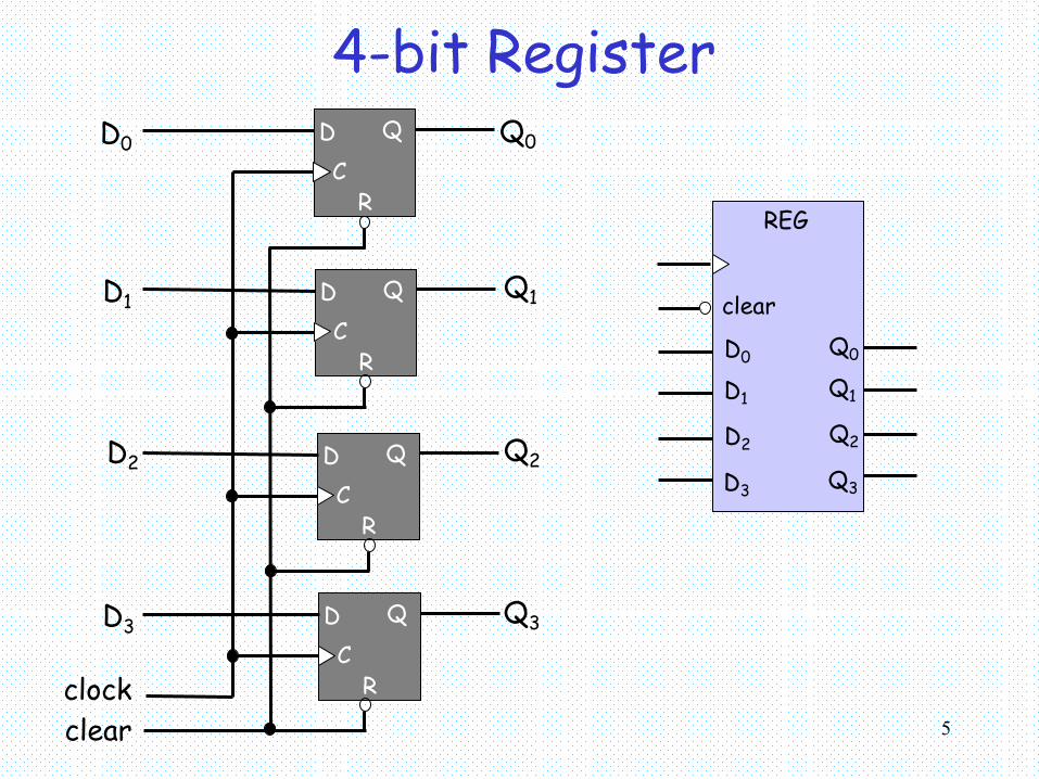
4-bit Register
REG
Q3
Q2
Q1
Q0
D3
D2
D1
D0
clear
D Q
clock
CR
D Q
CR
D Q
CR
D Q
CR
clear
D0
D1
D2
D3
Q0
Q1
Q2
Q3

6
Register with Parallel LoadLoad
D Q
CR
Q0
D Q
CR
Q1
D Q
CR
Q2
D Q
CR
Q3
clockclear
D1
D2
D3
D0

7
Loading Register
clock
C inputs
load
8
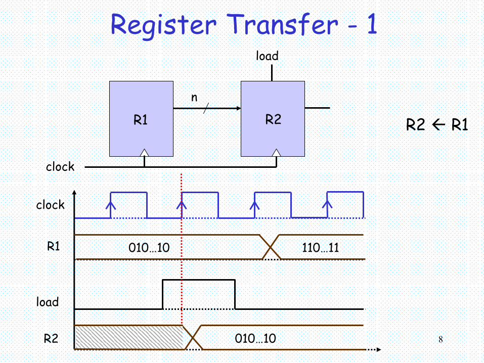
Register Transfer - 1
R1 R2n
load
clock
load
clock
R2 R1
R1 010…10 110…11
010…10R2
9
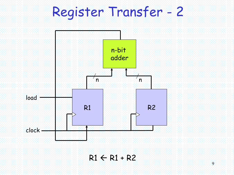
Register Transfer - 2
load
R1 R1 + R2
clock
R1 R2
n
n-bit adder
n
10
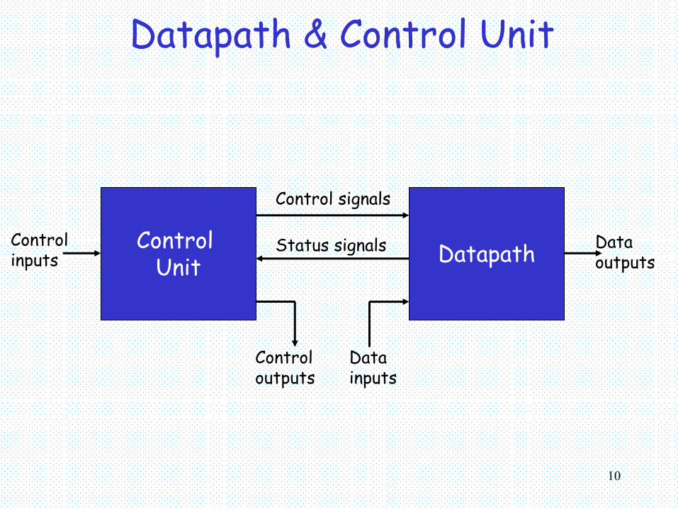
Datapath & Control Unit
Control Unit Datapath
Control signals
Status signalsControlinputs
Controloutputs
Dataoutputs
Datainputs

11
Shift Registers• A register capable of shifting its information in
one or both directions – Flip-flops in cascade
serial input
serial outputD Q
C
SID Q
C
D Q
C
D Q
C
SO
clock
• The current state can be output in n clock cycles

12
Serial Mode• A digital system is said to operate in serial mode
when information is transferred and manipulated one bit a time.
shift register A shift register BSOSI SI SO
clk clkclockshiftcontrol
clock
shift control
clkT1 T2 T3 T4
13
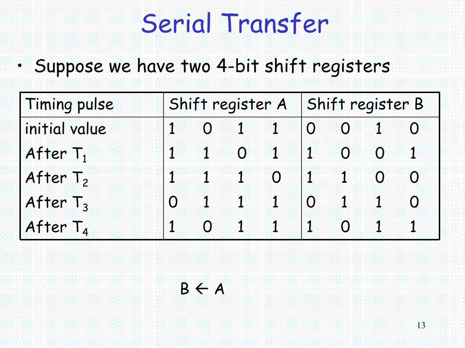
Serial Transfer• Suppose we have two 4-bit shift registers
11011101After T4
01101110After T3
00110111After T2
10011011After T1
01001101initial valueShift register BShift register ATiming pulse
B A

14
Serial Addition• In digital computers, operations are usually
executed in parallel, since it is faster• Serial mode is sometimes preferred since it
requires less equipment
shift register A
shift register B
SI
FAabC_in
S
C
DQ
C
SO
SO
SIserialinput
clockshiftcontrol
reset
15
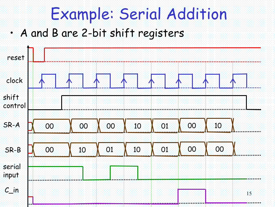
Example: Serial Addition
shift control
• A and B are 2-bit shift registers
reset
clock
00
10 01
00 10
10
01
01
serial input
00
00
10
00
SR-A
SR-B
C_in
00
00

16
Designing Serial Adder - 1
0X0X0X1X
11111010110110110001
X10111010010 X0
X010100X000000KQJQSQyxQ
Flip-flop inputsOutputNext stateInputsPresent state
Q(t+1) = JQ’ + K’Q
JQ = xy KQ = x’y’ = (x + y)’ S = x ⊕ y ⊕ Q

17
Designing Serial Adder - 2
SI
SIserialinput
shift register A
shift register B
clockshiftcontrol
JQ = xy KQ = x’y’ = (x + y)’ S = x ⊕ y ⊕ Q
reset
QJ
C
K
Sx
y
SO =
SO =

18
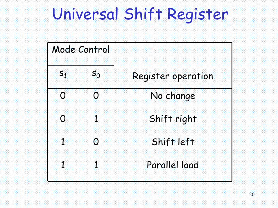
Universal Shift Register• Capabilities:
1. A clear control to set the register to 0.2. A clock input3. A shift-right control4. A shift-left control5. n input lines6. A parallel-load control 7. n parallel output lines8. A shift-control

19
Universal Shift Register
D
QCD
Q
CD
QCD
QC
A0A1A2A3
parallel outputs
clearclk
4×1MUX
0123
4×1MUX
0123
4×1MUX
0123
4×1MUX
0123
s1
s2
serialinput for shift-right
serial input for shift-left
parallel inputs
20
Universal Shift Register
Shift right10
Parallel load11
Shift left01
No change00
s0s1 Register operation
Mode Control

21
Counters• A counter is basically a register that goes
through a prescribed sequence of states upon the application of input pulses– input pulses are usually clock pulses
• Example: n-bit binary counter– count in binary from 0 to 2n-1
• Classification1. Ripple counters
• flip-flop output transition serves as the pulse to trigger other flip-flops
2. Synchronous counters• flip-flops receive the same common clock as the
pulse

22
Binary Ripple Counter
1 1 170 0 00
1 1 061 0 151 0 040 1 130 1 020 0 110 0 00
3-bit binary ripple counter
• Idea:– to connect the output of one flip-flop
to the C input of the next high-order flip-flop
• We need “complementing” flip-flops– We can use T flip-flops to obtain
complementing flip-flops or– JK flip-flops with its inputs are tied
together or– D flip-flops with complement output
connected to the D input.

23
4-bit Binary Ripple CounterT Q
CR
A0
T Q
CR
A1
T Q
CR
A2
T Q
CR
A3
clear
count
logic-1
D Q
CR
A0
D Q
CR
A1
D Q
CR
A2
D Q
CR
A3
clear
count

24
4-bit Binary Ripple Counter– Suppose the
current state is 1100
– What is the next state?
– A0 = 1 (0 1)– A1 = 1 (0 1)– A2 = 0 (1 0)– A3 = 1 – next state: 1011
• Binary count-down counter
T Q
CR
A0
T Q
CR
A1
T Q
CR
A2
T Q
CR
A3
clear
count
logic-1
25
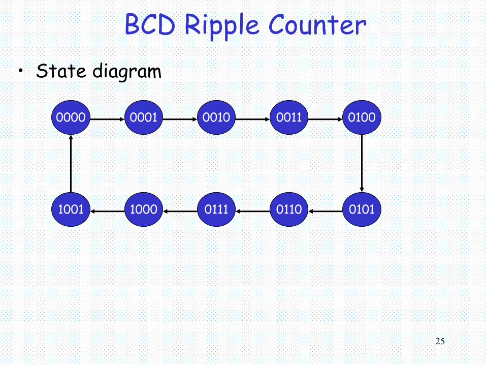
BCD Ripple Counter• State diagram
0000 0001 0010 0011 0100
1001 1000 0111 0110 0101
26
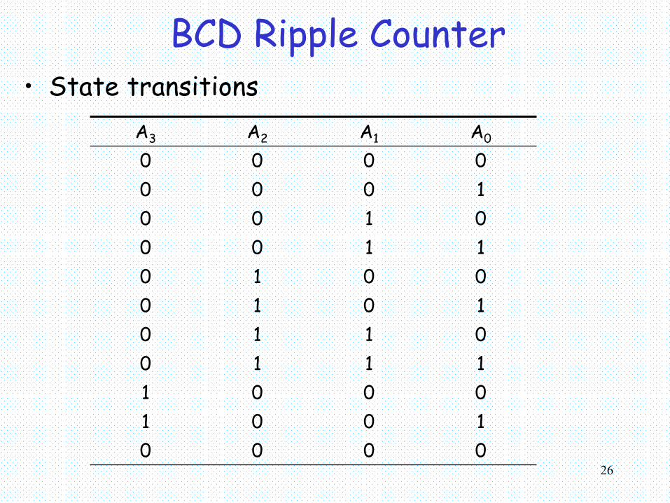
BCD Ripple Counter• State transitions
10010000
000111100110101000101100010010000000A0A1A2A3

27
BCD Ripple Counter with JK FFs
countJ Q
CA0
J QC
A1
J QC
A2
J QC
A3
K
K
K
K
logic-1

28
Multi-digit BCD Counter
BCD Counter
A0A1A2A3
count pulses
BCD Counter
A0A1A2A3
BCD Counter
A0A1A2A3
3-digit BCD counter
29
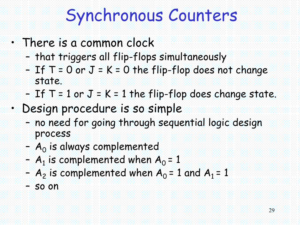
Synchronous Counters• There is a common clock
– that triggers all flip-flops simultaneously– If T = 0 or J = K = 0 the flip-flop does not change
state.– If T = 1 or J = K = 1 the flip-flop does change state.
• Design procedure is so simple– no need for going through sequential logic design
process– A0 is always complemented– A1 is complemented when A0 = 1– A2 is complemented when A0 = 1 and A1 = 1 – so on

30
4-bit Binary Synchronous CounterJ Q
CA0
J QC
A1
J QC
A2
J QC
A3
K
K
K
K
clock
countenable
to next stage
Polarity of theclock is notessential

31
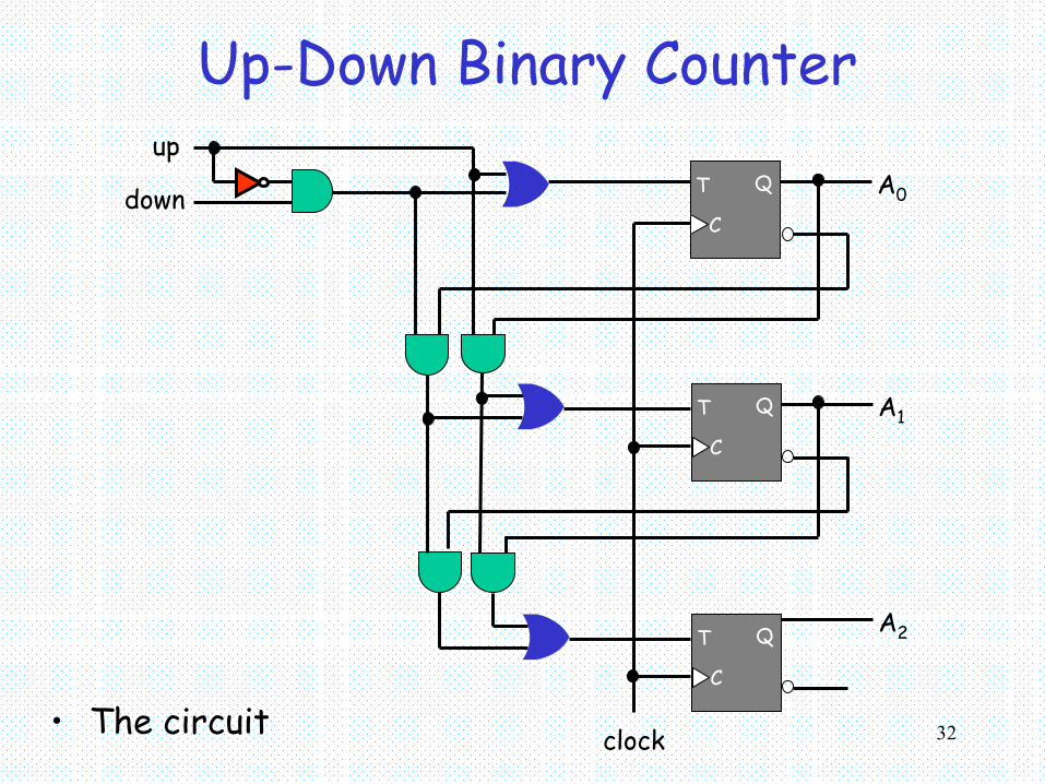
Up-Down Binary Counter• When counting downward
– the least significant bit is always complemented (with each clock pulse)
– A bit in any other position is complemented if all lower significant bits are equal to 0.
– For example: 0100 • Next state: 0011
– For example: 1100• Next state: 1011
32
Up-Down Binary Counter
• The circuit
T Q
C
A0
T Q
C
A1
T Q
C
A2
Cclock
up
down

33
Synchronous BCD Counter• Better to apply the sequential circuit design
procedure
001010101
11111111110
0010001000
1010000000
1000000000y
00001001100100010001111011100110011010101010001000101100110001000100100010000000
T1T2T4T8A1A2A4A8A1A2A4A8
Flip-Flop inputsoutputNext statePresent state

34
Synchronous BCD Counter• The flip-flop input equations
– T1 = 1– T2 = A8’ A1– T4 = A2A1– T8 = A8 A1 + A4 A2 A1
• Output equation– y = A8A1
• Cost– Four T flip-flops– four 2-input AND gates– one OR gate– one inverter

35
Binary Counter with Parallel Load
J QC
A0
J QC
A1
J QC
A2
K
K
K
clock
clear
countloadD0
D1
D2
carryoutput

36
Binary Counter with Parallel Load
no change00↑1
count up10↑1
load inputsX1↑1
clear to 0XXX0
FunctionCountloadclockclear
Function Table
37
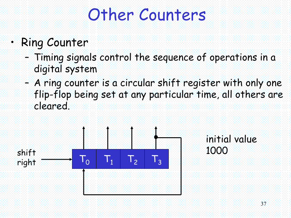
Other Counters• Ring Counter
– Timing signals control the sequence of operations in a digital system
– A ring counter is a circular shift register with only one flip-flop being set at any particular time, all others are cleared.
shift right T0 T1 T2 T3
initial value1000

38
Ring Counter• Sequence of timing signals
clock
T0
T1
T2
T3

39
Ring Counter
• To generate 2n timing signals, – we need a shift register with 2n flip-flops
• or, we can construct the ring counter with a binary counter and a decoder
2x4 decoder
T0 T1 T2 T3
2-bit countercount
Cost:• 2 flip-flop• 2-to-4 line decoderCost in general case: • n flip-flops• n-to-2n line decoder
• 2n n-input AND gates

40
Johnson Counter• A k-bit ring counter can generate k
distinguishable states• The number of states can be doubled if the shift
register is connected as a switch-tail ring counter
clock
D Q
C
D Q
C
D Q
C
D Q
C
X
X’
Y
Y’
Z
Z’
T
T’

41
Johnson Counter• Count sequence and required decoding
Z’T1000Y’Z1100X’Y1110XT1111ZT’0111YZ’0011XY’0001X’T’0000
87654321
TZYX OutputFlip-flop outputssequence
number

42
Johnson Counter• Decoding circuit
clock
D Q
C
D Q
C
D Q
C
D Q
C
X Y Z T
S0 S1 S2 S3 S4 S5 S6 S7

43
Unused States in Counters• 4-bit Johnson counter
0000 1000 1100
1110
111101110011
0001
0010 1001 0100
1010
110101101011
0101

44
Johnson Counter
00101001
OutputsInputs
00010010
1001010000001010101011011101011001101011101101010000100010001100110011101110111111110111011100110011000100010000TZYXTZYX
45
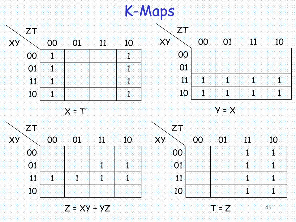
K-Maps
1110111111011100
10110100ZT
XY
X = T’
111110111111
0100
10110100ZT
XY
Y = X
101111111101
0010110100
ZTXY
Z = XY + YZ
1110111111011100
10110100ZT
XY
T = Z
46
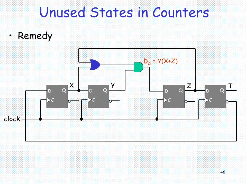
Unused States in Counters• Remedy
clock
D Q
C
D Q
C
D Q
C
D Q
C
X Y Z T
DZ = Y(X+Z)
47
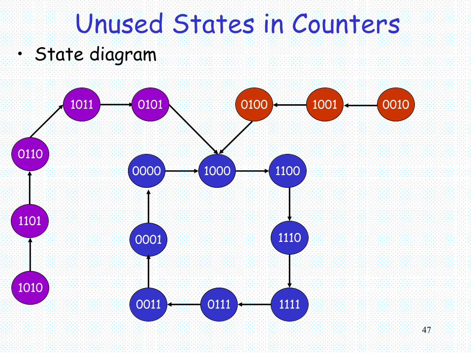
Unused States in Counters• State diagram
0000 1000 1100
1110
111101110011
0001
00100100 10011011 0101
0110
1010
1101