register-level design
TRANSCRIPT

Page 1
Register-Level Design
A digital system can be treated at different level of abstraction or complexity.So far, we have seen it at the gate level and the transistor level.
At a higher level than the gate level, we have the register level. The centralcomponent at this level is an n-bit storage device, or register.
Central Component
Transistor Level Transistor
Gate Level Logic Gate
Register Level Register
Higher levelof abstraction

Page 2
Logic Circuit for the 74X181 ALU

Page 3
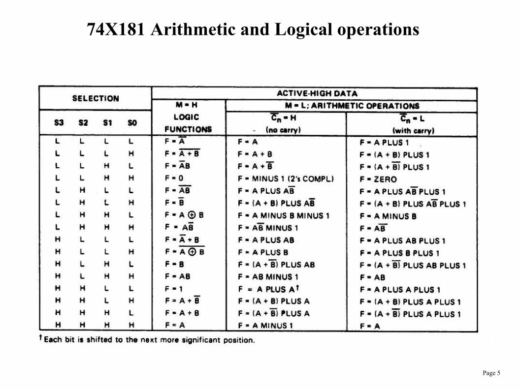
From the logic circuit for the 74X181, we can write
F 0=MC na0B0 S 0 B0 S1A0 B0 S 2A0 B0 S 3
which gives little information on what functions the circuit perform.
Using a truth table to describe the functions of the circuit is not a goodidea either as the circuit has 14 inputs, which means the truth table willhave 214=16384 rows!
The 74X181 is actually a 4-bit ALU which performs 32 different arithmeticand logical operations on two 4-bit inputs A=A3 A2 A1 A0 and B=B3 B2 B1 B0, producing the result F=F 3 F 2 F 1 F 0.
The operation to be performed is determined by the control signalsM and S=S 3 S 2 S1 S 0. In particular, the mode control signal M is set to 1 for logical operations, and 0 for arithmetic operations. Theselect control signal S is use to select the required operation.

Page 4
Register-Level Model of the 74X181 ALU
Page 5
74X181 Arithmetic and Logical operations
Page 6
Register-level design is geared toward the processing of words as thebasic units of information or signals. In contrast, in gate-level designindividual bits are treated as basic signals.
The word length is register-level design varies, but it is always a multiple of 4.
Another important aspect of register-level design is the data-flow representationwhich views the function of a digital circuit as processing data words that flowbetween computational and storage devices. The computational devices aretypically multifunction combinatorial circuits (e.g. the ALU), and the storagedevices are registers.
To manage these devices and control the data flow, control signals and circuitsthat generate these signals are required.
Page 7
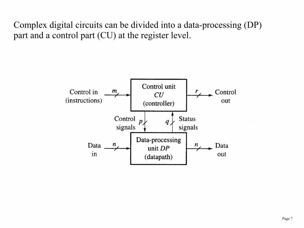
Complex digital circuits can be divided into a data-processing (DP)part and a control part (CU) at the register level.
Page 8
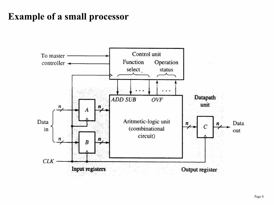
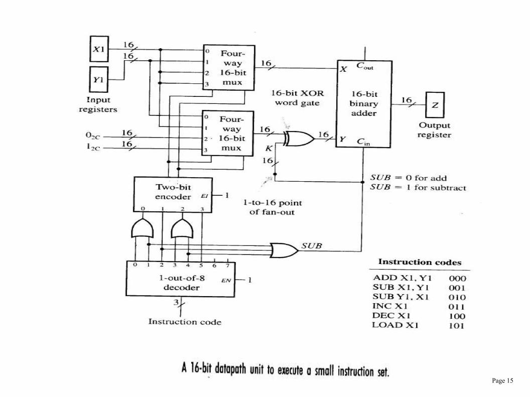
Example of a small processor
Page 9
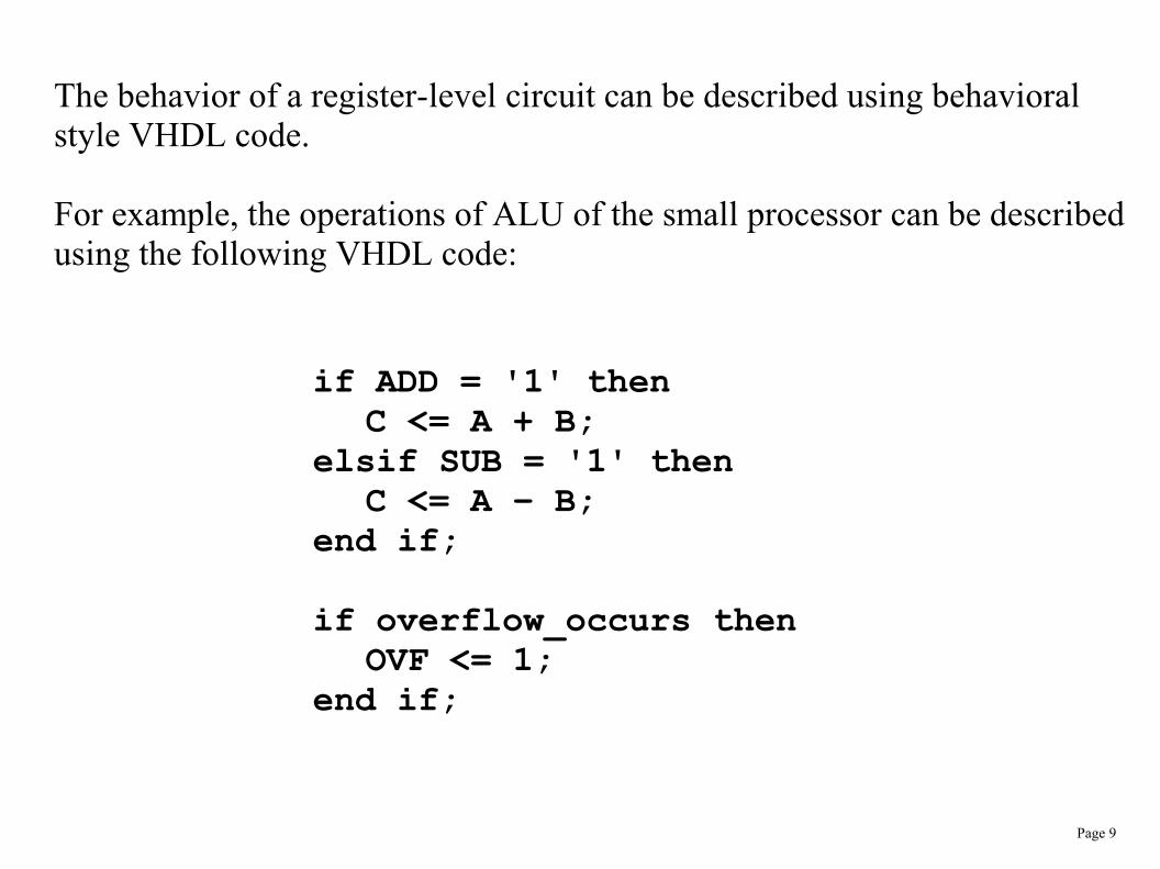
The behavior of a register-level circuit can be described using behavioralstyle VHDL code.
For example, the operations of ALU of the small processor can be describedusing the following VHDL code:
if ADD = '1' thenC <= A + B;
elsif SUB = '1' thenC <= A – B;
end if;if overflow_occurs then
OVF <= 1;end if;

Page 10
Basic components of register-level design:

Page 11
Component Expansion by Bit Slicing

Page 12
Shift Register Expansion using Bit Slicing

Page 13
Datapath Units (DP)
DP's are used to move and process data (in words).

Page 14
Page 15
Page 16
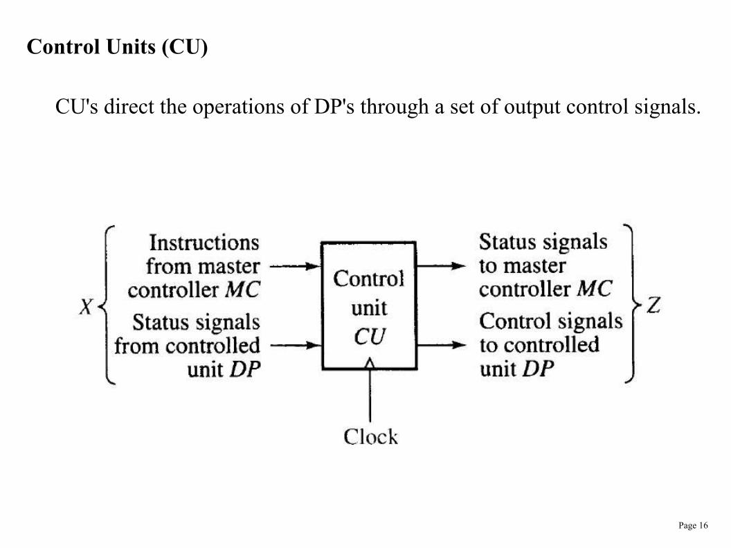
Control Units (CU)
CU's direct the operations of DP's through a set of output control signals.

Page 17
The Control Unit (CU) has a well-defined and fairly small set ofstates and is often implemented as a FSM.
Page 18
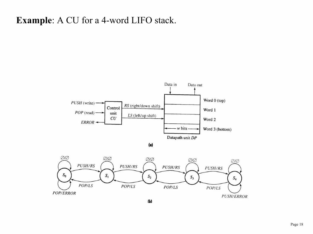
Example: A CU for a 4-word LIFO stack.
Page 19
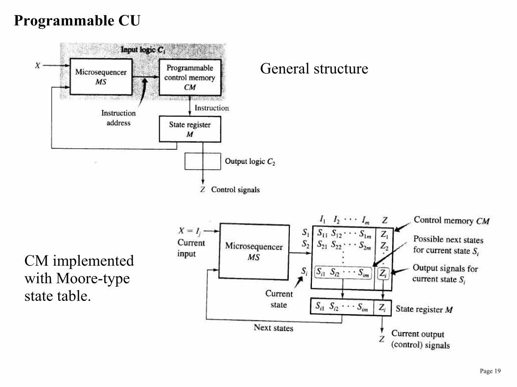
Programmable CU
General structure
CM implementedwith Moore-typestate table.

Page 20

Page 21
EPROM EPROMAddress Contents
a4 a3 a2 a1 a0 d7 d6 d5 d4 d3 d2 d1 d0push pop Present State Next Statew1 w0 y2 y1 y0 RS LS E Y2 Y1 Y00 0 0 0 0 0 0 0 0 0 00 0 0 0 1 0 0 0 0 0 10 0 0 1 0 0 0 0 0 1 00 0 0 1 1 0 0 0 0 1 10 0 1 0 0 0 0 0 1 0 00 0 1 0 1 x x x x x x0 0 1 1 0 x x x x x x0 0 1 1 1 x x x x x x0 1 0 0 0 0 0 1 0 0 00 1 0 0 1 0 1 0 0 0 00 1 0 1 0 0 1 0 0 0 10 1 0 1 1 0 1 0 0 1 00 1 1 0 0 0 1 0 0 1 10 1 1 0 1 x x x x x x0 1 1 1 0 x x x x x x0 1 1 1 1 x x x x x x1 0 0 0 0 1 0 0 0 0 11 0 0 0 1 1 0 0 0 1 01 0 0 1 0 1 0 0 0 1 11 0 0 1 1 1 0 0 1 0 01 0 1 0 0 0 0 1 1 0 01 0 1 0 1 x x x x x x1 0 1 1 0 x x x x x x1 0 1 1 1 x x x x x x1 1 0 0 0 x x x x x x1 1 0 0 1 x x x x x x1 1 0 1 0 x x x x x x1 1 0 1 1 x x x x x x1 1 1 0 0 x x x x x x1 1 1 0 1 x x x x x x1 1 1 1 0 x x x x x x1 1 1 1 1 x x x x x x
Alternative Programmable CU for the 4-Word LIFO Stack
Page 22
The Architecture Level
At the next higher level, we have the architecture level. This level dealswith memories and processing units that store and process blocks ofdata words known as program instructions and program data.
The interconnection of the digital system to the outside world is alsodealt with at this level through input/output circuits.
The major components at this level are: CPU, memory and I/O circuits.The operations of these components are determined by executing a seriesof control words, or program instructions.

Page 23
The primary function of the CPU is to fetch instructions from themain memory and execute them.
CPUM

Page 24
The CPU can be divided into 2 parts: the control part and the data part.
The control part is called the instruction unit (I-unit). It contains aninstruction register (IR), a program counter (PC), an instructiondecoder.
The data part is called the execution unit(E-unit). It contains at least a datapathand a set of registers for temporary datastorage. Some E-units also contain afast local memory called the cache memory.
Page 25
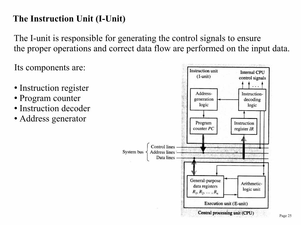
The Instruction Unit (I-Unit)
The I-unit is responsible for generating the control signals to ensurethe proper operations and correct data flow are performed on the input data.
Its components are:
● Instruction register● Program counter● Instruction decoder● Address generator

Page 26
In order to perform computing operations, a CPU executes instructions froma program written in its machine language. The machine language of a CPUis simply a collection of instructions (called the instruction set) that defineall the possible operations of the CPU.
A typical sequence of operations performed by the I-Unit is:
1. Load the location (address) of the first instruction of the program into the Program Counter (PC).
2. Load the instruction into the Instruction Register (IR).
3. Initiate the instruction decoder to decode the instruction so that the appropriate control and address signals for the datapath unit are generated.
4. Increment the value of the Program Counter (PC) by 1.
5. Repeated Steps 2 to 4 until the end of the program is reached.

Page 27
The datapath consists of at least 2 main components: the register file, andthe ALU.
● The ALU performs logical and arithmetic operations on the input data.● The register file provides a set of fast local storage locations.
The interconnections of these units determine the allowable data flow paths.The properties of these units and how they are connected together definethe architecture of the CPU.
Some datapaths also contain a local memory called the cache memory. Itallows the CPU to access the main memory (M) more efficiently.

Page 28
The instruction set of a CPU is determined by its architecture.
Instruction Set
A machine language instruction is a binary-encoded word. In other words,it is just a binary code. The code is derived from the property of the datapathand the data flow paths.
A machine language instruction usually consists of two parts: the opcodeand the operand. Some instructions do not have operands.
For example:
The processor in Lab 7 uses 8-bit machine language instructions. Forinstructions with operands, the most significant 4 bits used as opcode and theremaining 4 bits as operand. For instructions without operands, the mostsignificant 4 bits and the least significant bit form a 5-bit opcode.

Page 29
The instruction set of a typical commercial CPU is quite large, but can becategorized into the following groups:
1. Data-transfer instructions(load, store and I/O)
2. Data-processing instructions(arithmetic and logic operations)
3. Program-control instructions(conditional and unconditional branching)
Page 30
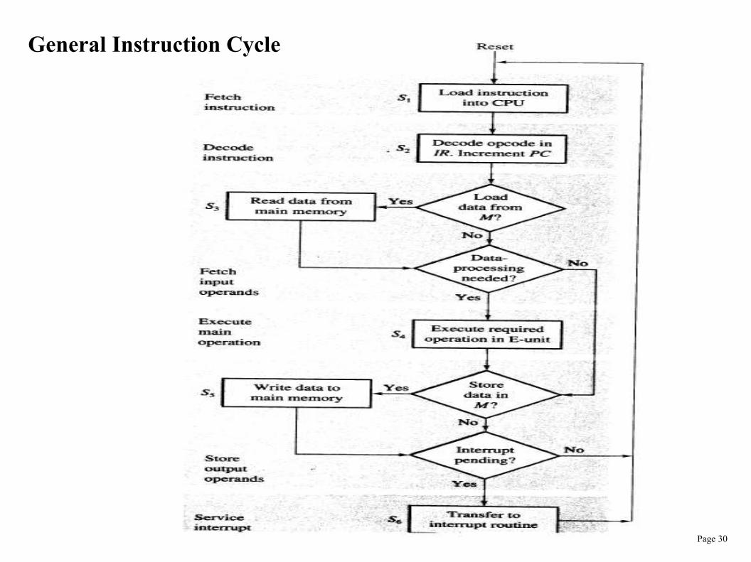
General Instruction Cycle

Page 31
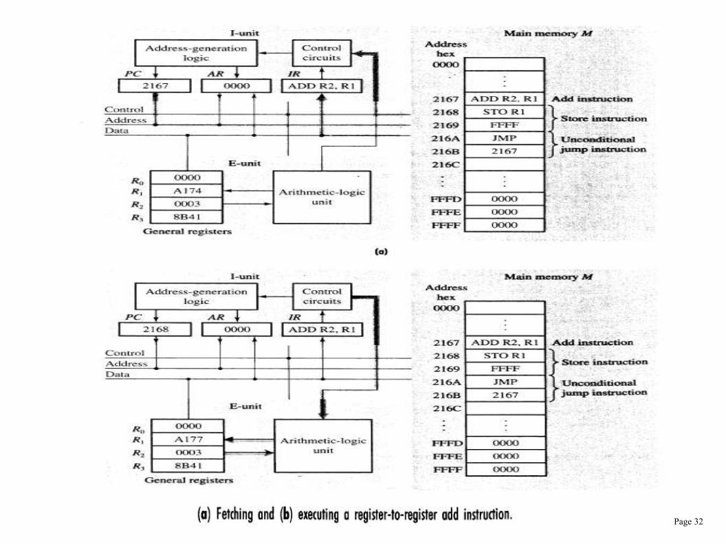
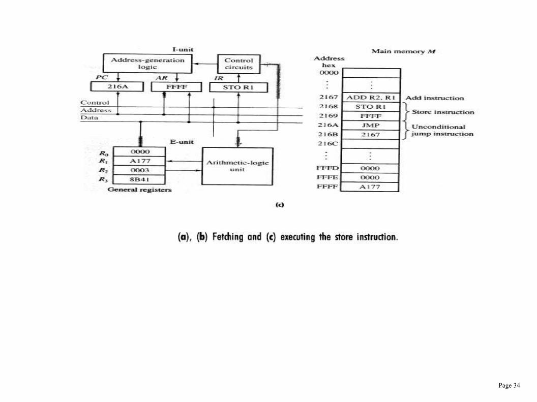
Program Segment:
ADD R2, R1 ; R1 := (R1) + (R2)
STO R1, FFFF ; (FFFF) := R1
JMP 2167 ; Jump to address 2167
Example:
Page 32

Page 33
Page 34

Page 35
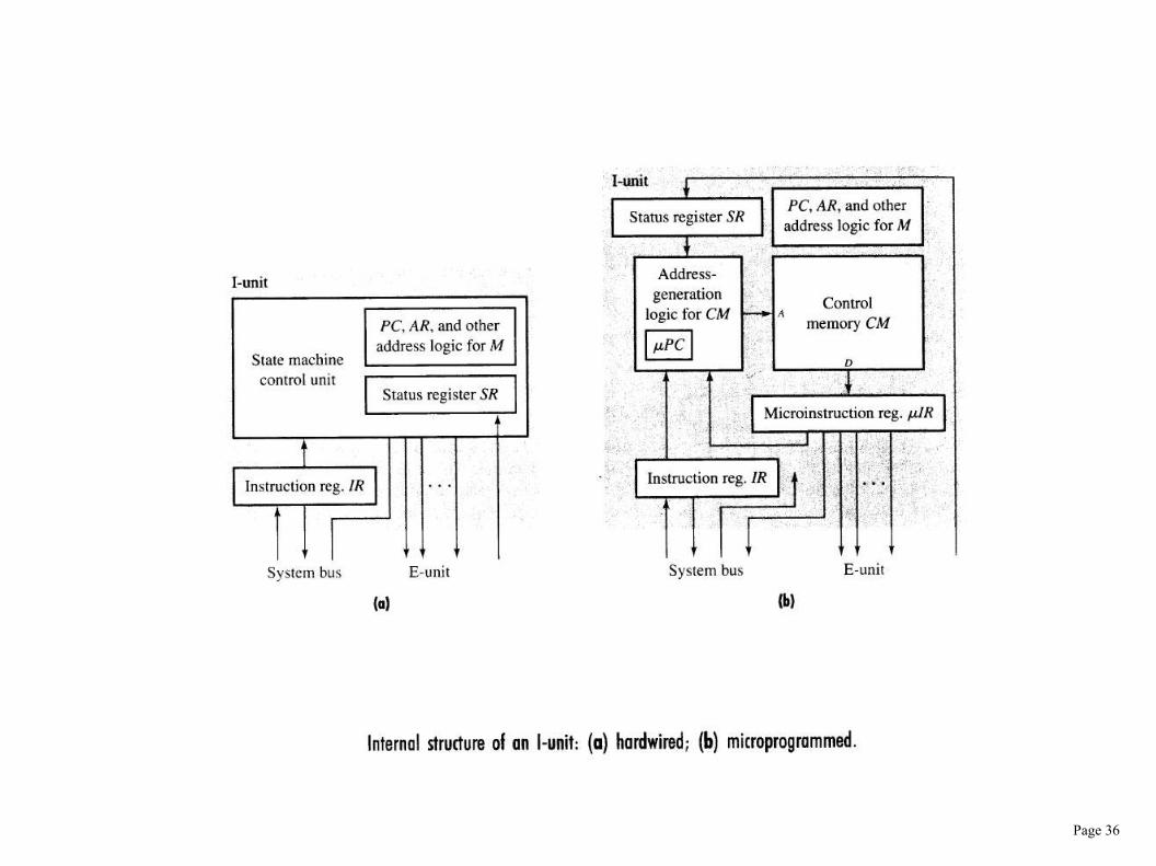
Structure of Typical I-Units
The I-unit is responsible for controlling the entire instruction cycle.The actions to be taken depend on the instructions being executed.
An I-unit may be either hardwired, or microprogrammed.
Hardwired I-units: amount of hardware is minimized, speed is maximized.
Microprogrammed I-units: flexible and expandable.
Page 36

Page 37
In a microprogrammed I-unit, the machine language instruction of the processor is used to access a microcode sequence to perform a series of operations. The microcode sequence is stored in a microcode ROMcalled the control memory (CM).
The microcode basically contain values of control signals for the CPU.
Page 38
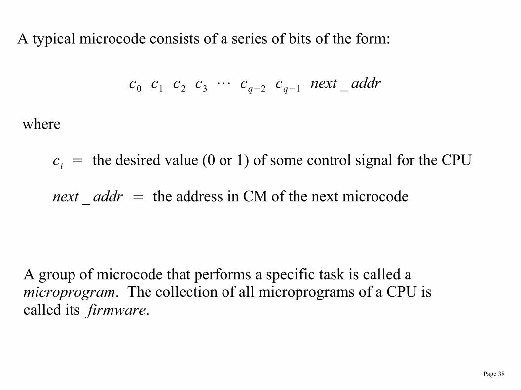
A typical microcode consists of a series of bits of the form:
c0 c1 c2 c3 ⋯ cq−2 cq−1 next _ addr
ci = the desired value (0 or 1) of some control signal for the CPU
where
next _ addr = the address in CM of the next microcode
A group of microcode that performs a specific task is called amicroprogram. The collection of all microprograms of a CPU iscalled its firmware.