reference design for uhf ask/fsk transmitter ata5756 and...
TRANSCRIPT

NOTE: This is a summary document. The complete document is available. For more information, please contact your local Atmel sales office.
Transmitter ICs ATA5756 and ATA5757
Application Note
Summary
4835BS–RKE–07/07
Reference Design for UHF ASK/FSK Transmitter ATA5756 and ATA5757
Features• PLL Transmitter IC With Single-ended Output• High Output Power (6 dBm) at 8.1 mA (315 MHz) and 8.5 mA (433 MHz) Typical Values• Divide by 24 (ATA5756) and 32 (ATA5757) Blocks for 13-MHz Crystal Frequencies and
for Low XTO Start-up Times• Modulation Scheme ASK/FSK With Internal FSK Switch• Up to 20 kBaud Manchester Coding, Up to 40 kBaud NRZ Coding• Power-down Idle and Power-up Modes to Adjust Corresponding Current Consumption
through ASK/FSK/ENABLE Input Pins• ENABLE Input for Parallel Usage of Controlling Pins in a 3-wire-bus System• CLK Output Switches ON if the Crystal Current Amplitude has Reached 35% to 80% of
its Final Value• Crystal Oscillator Time Until CLK Output is Activated, Typically 0.6 ms• Supply Voltage 2.0V to 3.6V in Operation Temperature Range of –40°C to +125°C• ESD Protection at All Pins (4 kV HBM)• Small Package, TSSOP10
Benefits• Integrated Low Parasitic FSK Switch• Very Short and Reproducible Time to Transmit, Typically < 0.85 ms• 13.125-MHz/13.56-MHz Crystals Make Small Package Sizes Possible
1. DescriptionThe reference design PCB (demo board) using the Atmel ATA5756/ATA5757 trans-mitter ICs meets the requirements of dedicated short range device (SRD) applicationssuch as tire pressure monitoring systems (TPMS) and remote keyless entry (RKE).For extended evaluation purposes, a 50Ω SMB connector is available. Assembly andmatching recommendations are provided. Using the on-board (commonly used) inte-grated printed loop antenna, a radiated power of –13.2 dBm effective radiated power(e.r.p.) at 315 MHz and –15.0 dBm e.r.p. at 433.92 MHz is achieved. The typicalAtmel® demo boards ATAB5756 and ATA5757 have been tested in an authorizedTest house under the requirements of FCC part15 and EN 300 220. This test showsthat a type approval based on FCC part15 as well as EN 300 220 could be achievedwith the transmitter.
The selected quartz crystals from two manufactures are compliant with the challeng-ing TPMS demands covering the environmental conditions and provide the bestperformance for the transmitter. For this purpose, a crystal selection guide is alsoincluded in this document. This application note explains technical issues useful dur-ing the design phase of this transmitter type. Some of these technical issues are of ageneral nature and also useful for other transmitters.

2. Description of ATA5756/ATA5757The ATA5756/ATA5757 is a PLL transmitter IC which has been developed for the demands ofRF low-cost transmission systems at data rates up to 20 kBaud (Manchester coding) and40 kBaud (NRZ coding). The transmitting frequency range is 313 MHz to 317 MHz (for theATA5756) and 432 MHz to 448 MHz (for the ATA5757). It can be used in both frequency shiftkeying (FSK) and amplitude shift keying (ASK) systems. Due to its short crystal oscillator settlingtime, it is well suited for TPMS and for passive entry go (PEG) applications.
Figure 2-1. System Block Diagram
3. Pin Configuration
Figure 3-1. Pinning TSSOP10
IF Amp
LNA VCO
PLL XTO
Control
U3741B/ U3745B/ T5743/ T5744
1...3
Mic
roco
ntro
ller
UHF ASK/FSK Remote Control Receiver
Demod.
Antenna Antenna
PLL
ATA5756/ATA5757
UHF ASK/FSK TPM and Remote Control
Transmitter1 Li cell
Keys
VCO
Power amplifier
VCO
Encoder ATARx9x
1
2
3
10
9
8
7
CLK
ASK
FSK
ANT2
ENABLE
GND
VS
XTO1
ATA5756 ATA5757
5ANT1 6 XTO2
4
24835BS–RKE–07/07
ATA5756/ATA5757

ATA5756/ATA5757
4. Demo Board
Figure 4-1. Demo Board Schematic
VD
D
BP
40/S
C/IN
T3
1 2 3 4 5 6 7 8 9 10
20 19 18 17 16 15 14 13 12 11
VS
S
BP
53/IN
T1
OS
C1
BP
10
X1
X1X2X3X4X5X6X7X8
D1D2D3D4D5D6D7D8
VS
D1
0
0BR
4B
R5
U2
EN
1F
SK
1
AS
K1
CLK
1
BR
3
BR
2
1
2
3
S1
EN
GN
D
VS
XT
O1
XT
O2
CLK
AS
K
FS
K
AN
T2
AN
T1
109876
VS
Q1
C3
C2
C1
0
U1
12345
X4
X3
C16
VS 0
BA
2032
SM 1 2
VS
C4
C5
0
C6
L1
Loop
Ant
enna
P
CB
V1.
0 30
mm
× 2
0 m
m
BP
52/IN
T1
BP
51/IN
T6
BP
50/IN
T6
OS
C2
BP
60/T
30
BP
43/S
D/IN
T3
BP
42/T
20B
P41
/T2I
/VM
IB
P23
BP
22B
P21
BP
20/N
TE
BP
63/T
3I/IN
T5
BP
13
0
0
+ -
0
L2
C8
C9
C10
C11
C12
C13C
70X
2
BR
1
R1
00
C14
C15
0 0
11
2 2
3 3
4 4 4
S2
S3
34835BS–RKE–07/07
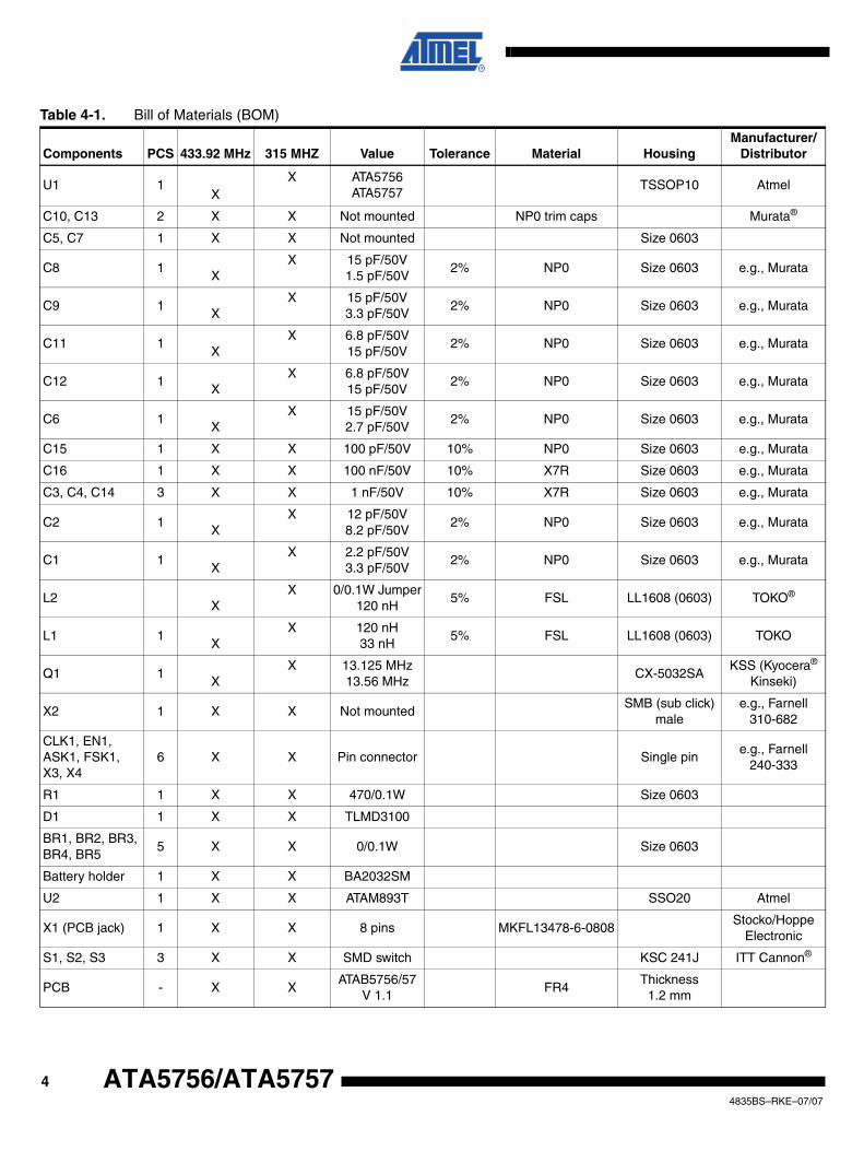
Table 4-1. Bill of Materials (BOM)
Components PCS 433.92 MHz 315 MHZ Value Tolerance Material HousingManufacturer/
Distributor
U1 1X
X ATA5756ATA5757
TSSOP10 Atmel
C10, C13 2 X X Not mounted NP0 trim caps Murata®
C5, C7 1 X X Not mounted Size 0603
C8 1X
X 15 pF/50V1.5 pF/50V
2% NP0 Size 0603 e.g., Murata
C9 1X
X 15 pF/50V3.3 pF/50V
2% NP0 Size 0603 e.g., Murata
C11 1X
X 6.8 pF/50V15 pF/50V
2% NP0 Size 0603 e.g., Murata
C12 1X
X 6.8 pF/50V15 pF/50V
2% NP0 Size 0603 e.g., Murata
C6 1X
X 15 pF/50V2.7 pF/50V
2% NP0 Size 0603 e.g., Murata
C15 1 X X 100 pF/50V 10% NP0 Size 0603 e.g., Murata
C16 1 X X 100 nF/50V 10% X7R Size 0603 e.g., Murata
C3, C4, C14 3 X X 1 nF/50V 10% X7R Size 0603 e.g., Murata
C2 1X
X 12 pF/50V8.2 pF/50V
2% NP0 Size 0603 e.g., Murata
C1 1X
X 2.2 pF/50V3.3 pF/50V
2% NP0 Size 0603 e.g., Murata
L2X
X 0/0.1W Jumper120 nH
5% FSL LL1608 (0603) TOKO®
L1 1X
X 120 nH33 nH
5% FSL LL1608 (0603) TOKO
Q1 1X
X 13.125 MHz13.56 MHz
CX-5032SAKSS (Kyocera®
Kinseki)
X2 1 X X Not mountedSMB (sub click)
malee.g., Farnell
310-682
CLK1, EN1, ASK1, FSK1, X3, X4
6 X X Pin connector Single pine.g., Farnell
240-333
R1 1 X X 470/0.1W Size 0603
D1 1 X X TLMD3100
BR1, BR2, BR3, BR4, BR5
5 X X 0/0.1W Size 0603
Battery holder 1 X X BA2032SM
U2 1 X X ATAM893T SSO20 Atmel
X1 (PCB jack) 1 X X 8 pins MKFL13478-6-0808Stocko/Hoppe
Electronic
S1, S2, S3 3 X X SMD switch KSC 241J ITT Cannon®
PCB - X XATAB5756/57
V 1.1FR4
Thickness 1.2 mm
44835BS–RKE–07/07
ATA5756/ATA5757

ATA5756/ATA5757
4.1 Layout
Figure 4-2. Top Layer
Figure 4-3. Bottom Layer
54835BS–RKE–07/07
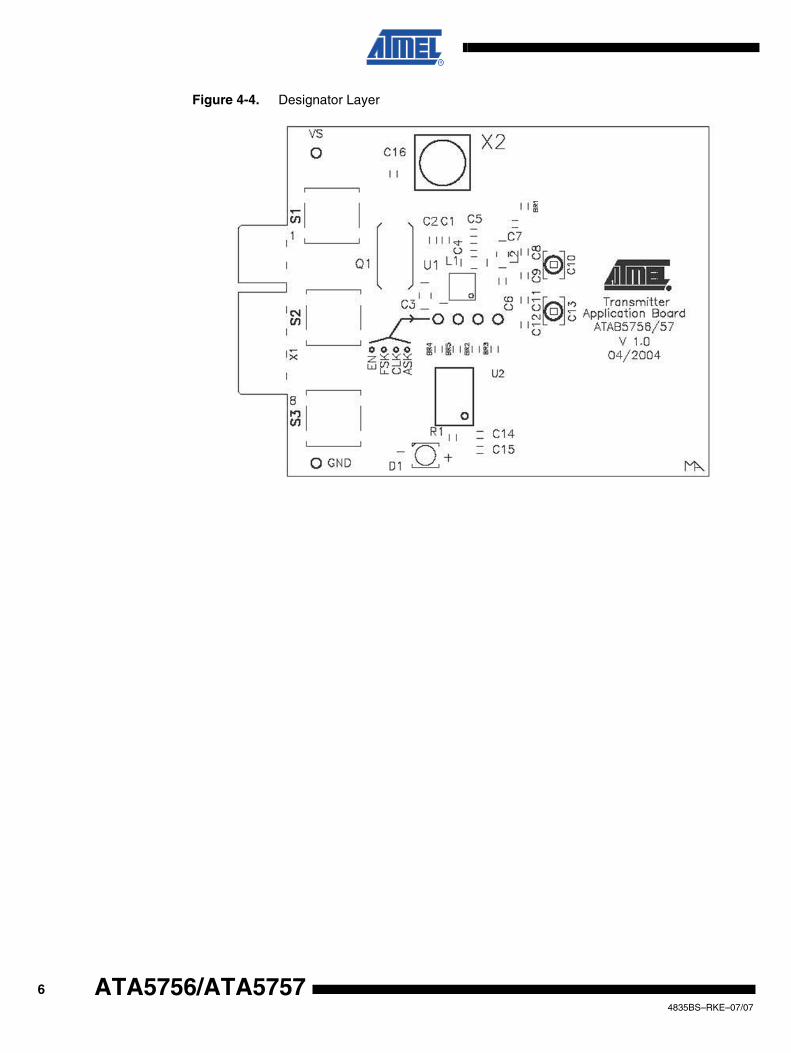
Figure 4-4. Designator Layer
64835BS–RKE–07/07
ATA5756/ATA5757

ATA5756/ATA5757
4.2 Using the RF Design Kit and Demo BoardFor development purposes, Atmel provides a demo board for the transmitter together with amicrocontroller board with which the transmitter (or receiver, as the case may be) can be pro-grammed. In order to program the transmitter, an Atmel 4-bit microcontroller for stand-aloneoperation, a microcontroller board with AVR®, and the Windows®-based software, RF DesignKit, will be needed. Figure 4-5 shows the RF Design Kit software after startup.
Figure 4-5. RF Design Kit Software
Atmel’s transmitter types (in this example, ATA5756) can be chosen from the pull-down menuTransmitter. After specifying a transmitter, the list of the parameters that can be set appears.Choosing Telegram activates the window in Figure 4-6 on page 8.
74835BS–RKE–07/07

Figure 4-6. Menu Telegram in RF Design Kit
The Telegram menu is used to set the modulation types (ASK or FSK), the data rate, preburst,and the test word to be sent from the transmitter (Figure 4-7). The Programmable Push But-tons menu is used to set the functionality of each button on the demo board. Each button canenable the sending of a continuous telegram, a single telegram, a continuous pattern, a singlepattern, and, of course, a continuous carrier. The continuous transmission takes about 30s. Thelist of alternatives is implemented in a pull-down menu for each button (shown in Figure 4-8 onpage 9).
84835BS–RKE–07/07
ATA5756/ATA5757

ATA5756/ATA5757
Figure 4-7. Programmable Push Button Menu
Figure 4-8. Contents of the Pull-down Menu for Functionality of Each Button
The menu Pattern (Figure 4-9) is used to set the pattern of the data to be sent and the modula-tion types. The last menu is Application (Figure 4-10 on page 10); this menu shows theschematic of the general transmitter's application on the demo board. In addition to the sche-
94835BS–RKE–07/07

matic, the user can check the defined timing for ASK/FSK and the recommended settings forAtmel's receiver application, which work well with the transmitter.
Figure 4-9. Pattern Menu
Figure 4-10. Application Menu
For more information, refer to the documents Software Description RF Design Kit and HardwareDescription RF Design Kit, available on the demo software CD-ROM or on Atmel’s website.
104835BS–RKE–07/07
ATA5756/ATA5757
ATA5756/ATA5757
5. Application Hints
5.1 Antenna Selection and DesignDifferent applications and frequency bands require different antenna solutions. Short rangedevices (SRD) in the ISM bands around 315 MHz and 433.92 MHz use mostly quarter-wavemonopoles, helical antennas, or printed small-loop antennas. The characteristic antenna data(such as directivity, gain, polarization, impedance, and bandwidth) determines the application.Cost is one of the most significant parameters for mass production.
For use in remote keyless entry (RKE) devices, or, more generally, hand-held devices for wire-less control transmitters, the printed small-loop antenna is free of cost. It also has a sufficientperformance, the hand-sensitivity is little, and the size is small.
Certain tire pressure monitoring systems (TPMS) currently use the valve as radiator element— a short quarter-wave monopole. Advantages include the double usage of the valve asantenna and the higher gain of the monopole. Since the radiation starts outside the rim, the linkbudget to the RF receiver is much better. A side effect is the influence of the actual rim of the tireon the radiation pattern and antenna impedance. The placement of a small-loop antenna radiat-ing from inside the rim results in a sufficient link budget, but without these drawbacks. A furtheradvantage is improved ESD protection, since there is no possibility for the user to come in con-tact with the transmitter module during maintenance.
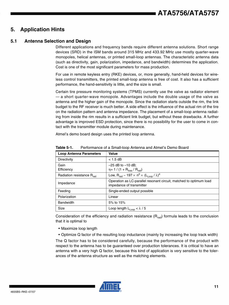
Atmel’s demo board design uses the printed loop antenna.
Consideration of the efficiency and radiation resistance (Rrad) formula leads to the conclusionthat it is optimal to
• Maximize loop length
• Optimize Q factor of the resulting loop inductance (mainly by increasing the loop track width)
The Q factor has to be considered carefully, because the performance of the product withrespect to the antenna has to be guaranteed over production tolerances. It is critical to have anantenna with a very high Q factor, because this kind of application is very sensitive to the toler-ances of the antenna structure as well as the matching elements.
Table 5-1. Performance of a Small-loop Antenna and Atmel’s Demo Board
Loop Antenna Parameters Value
Directivity < 1.5 dB
GainEfficiency
–25 dB to –10 dB; η = 1 / (1 + Rloss / Rrad)
Radiation resistance Rrad Low, Rrad ~ 197 × n2 × (LLoop / λ)4
ImpedanceOperation as LC-parallel resonant circuit, matched to optimum load impedance of transmitter
Feeding Single-ended output possible
Polarization Linear
Bandwidth 5% to 15%
Size Loop length LLoop < λ / 5
114835BS–RKE–07/07

The definition of the small-loop antenna is valid up to a length < λ / 5 and the high Q factor andbandwidth must meet the demands for mass production.
The Atmel reference board V1.1 shows an example for a design compromise:
• Loop length ~ λ / 7 (for the 433.92 MHz application), λ / 9 (315 MHz application)
• Loop width = 1.1 mm
• Resulting efficiency is η = –17 dBi to –19 dBi
For more information please see Section “Layout” on page 5
Figure 5-1 shows the inductance loop versus trace width of the loop for two lengths: LnH5 = λ / 5and LnH10 = λ / 10.
The formula for the inductance is
where l represents the trace length of the loop,
with I / width > 50, and k = 1.07 for a circle or k = 1.47 for a square loop
Figure 5-1. Inductance LLoop versus Loop Width for Two Loop Lengths: LnH5 = λ / 5 and LnH10 = λ / 10
Figure 5-2 on page 13 shows the loop antenna efficiency of a copper trace (length LnH5 = λ / 5)versus loop width.
LLoop/ nH 2 l / cm× lnl
width--------------⎝ ⎠
⎛ ⎞ k– ;×=
0.0
50.0
100.0
150.0
200.0
250.0
0.0E+00 5.0E-04 1.0E-03 1.5E-03 2.0E-03
Width (m)
L_l
oo
p/n
H
LnH5
LnH10
η 1
1Rloss
Rrad-------------+⎝ ⎠
⎛ ⎞----------------------------=
124835BS–RKE–07/07
ATA5756/ATA5757

ATA5756/ATA5757
Figure 5-2. Efficiency of the Copper Trace
Generally, the loop should not be routed over a ground plane. But, in case of space constraints,the loop can overlap the entire PCB circuit and achieve sufficient performance.
5.2 Understanding the Load Impedance of the Antenna and Matching of the Power Amplifier to Achieve the Optimal Transmit Power
The load impedance is defined as the impedance seen from pin ANT1 and pin ANT2 into thematching network (Figure 5-3).
Note: Do not confuse this large-signal load impedance with the small-signal input impedance delivered as an input characteristic of RF amplifiers. The latter is measured from the application into the IC instead of from the IC into the application for a power amplifier.
Figure 5-3. Definition of the Load Impedance
0.0
10.0
20.0
30.0
40.0
50.0
60.0
70.0
80.0
0.0E+00 5.0E-04 1.0E-03 1.5E-03 2.0E-03
Width (m)E
ff (
%)
PA
Ant1
Ant2
Load impedance
L1
C4
134835BS–RKE–07/07

5.2.1 Theory of Output Matching for ATA5756/ATA5757The power amplifier (PA) is an open collector output delivering a current pulse which is nearlyindependent from the load impedance, and can therefore be controlled via the connected loadimpedance. The maximum output power is delivered to a resistive load if the 0.66 pF outputcapacitance of the PA is compensated by the reactive part of the load impedance and the volt-age amplitude is as high as possible without saturating the output transistor (Vce sat = 0.8V).
Figure 5-4. The Principle of Matching for the PA
5.2.1.1 Output Matching to the Loop AntennaSection 5.1 described the antenna section and design information specifically for loop antennas.This section explains the matching method of the loop antenna to the transmitter; for this pur-pose, the formulas are included.
In order to optimize the matching structure, an s-parameter–based RF simulation tool can beused. In most cases, the measured s-parameter of the designed loop structure can be importedinto the simulation tool. The results with a tolerance of ±5% are accurate enough to work with.Professional CAD tools offer libraries for complete L, C series of different manufacturers. Forstarting values, consider Figure 5-5.
Figure 5-5. Equivalent Circuit for a Loop Antenna
0.66 pF
VS = 3V
Vce sat = 0.8V
8 mA
I(t)ZLoadOptI(t)
V(t)
V(t)
Loop
Rloss
Rrad
Cmatch1
Cmatch2
Zload
ZII
144835BS–RKE–07/07
ATA5756/ATA5757

ATA5756/ATA5757
• Z || (parallel resonance impedance) at transmitting frequency.
• ZLoad = RLoadOpt. The capacitors Cmatch 1, Cmatch 2 perform the transformation according to the listed equations (r = ratio).
(M.1) Z || = Q × 2πf × LLoop
(M.2) Z || ≈ r2 × Zout
(M.3)
(M.4)
(M.3) and (M.4) ---> Cmatch1 = r × C||
The grounding of the matching and filter stage has a great impact on the rejection of harmonics.The layout of the Atmel reference board shows double and quadruple vias to the ground plane inorder to reduce the inductive reactance of the vias. Using simulators, the increase of the realpart of the impedance in the range > 1 GHz can be seen — a pretty good radiation condition,also for parasitic radiators on the application.
The usage of two serial capacitors is useful to achieve more accurate values for the fine tuningdecreasing the influence of the capacitors’ tolerances.
5.2.1.2 Output Matching to 50Ω SMB ConnectorThis section describes the method of the matching for 50Ω.
The output power is set by the load impedance looking towards the antenna. The maximumoutput power is achieved with a load impedance of
• ZLoadOpt = 380 + j340 (ATA5756) at 315 MHz
• ZLoadOpt = 280 + j310 (ATA5757) at 433.92 MHz
(For more information, please refer to the datasheet.)
A low resistive path to VS is required to deliver the DC current. If the 0.66 pF output capacitanceis absorbed into the load impedance, a real impedance of RLoadOpt = 684Ω (ATA5756) at315 MHz and RLoadOpt = 623Ω (ATA5757) at 433.92 MHz should be measured with a networkanalyzer at pin 5 (ANT1) with the ATA5756/ATA5757 soldered. For this measurement the poweramplifier must be switched off.
ATAB5756/ATAB5757 also includes the possibility for detailed performance tests at 50Ω termi-nation. Different connectors are possible.
Connector assembly:
• Replace all components of the matching except C4/C5 with the elements on the Table 5-2 on page 16
• Place a jumper at C7
CII1
ω02
LLoop×------------------------------
Cmatch1 Cmatch2×Cmatch1 Cmatch2+-----------------------------------------------= =
rCmatch1 Cmatch2+
Cmatch2-----------------------------------------------= ---> 1
r---
Cmatch2
Cmatch1 Cmatch2+-----------------------------------------------=
154835BS–RKE–07/07

The following paragraphs describe the matching and measuring method to 50Ω.
The list below names the instruments mentioned in the next paragraphs.
• Network analyzer (NWA) 8753E (Agilent®)
• Spectrum analyzer E4403B (Agilent)
• Semi-rigid cable
• 50Ω RF connecting cable with damping factor of 0.5 dB at 315 MHz
Figure 5-6 shows the principle of the transmit power measurement assembly with matching to50Ω.
Figure 5-6. Measurement Assembly Measuring the Output Power at 50Ω Matching
If the requirement of the matching is met, the impedance (ZLoad) seen from ANT1 is equalto ZLoadOpt (refer to the datasheet ATA5756/ATA5757, for example ZLoadOpt is 380Ω + j340Ω for315 MHz).
Note: Because the layout of the application board has an influence on the matching, the values of the matching elements should be optimized for every new design.
Table 5-2. Matching Elements for 50Ω on Atmel's Demo Board
315 MHz Application 433.92 MHz Application
L1 = 68 nHC2 = 2.2 pF
L1 = 39 nHC2 = 1.8 pF
ANT1
ANT2
L1
C2
C1 = 1 nF
50Ω
ZLoadOpt
Spectrum Analyzer
164835BS–RKE–07/07
ATA5756/ATA5757

ATA5756/ATA5757
The following steps are very useful for matching the transmitter type (here as an example forATA5756) to 50Ω.
First step: finding the ZLoad that meets the required ZLoadOpt with a network analyzer (NWA)
Figure 5-7. Measuring the Load Impedance of the Demo Board With a Network Analyzer
For this purpose, the semi-rigid cable and the 50Ω cable should be properly calibrated. The cali-bration will be performed using a network analyzer (NWA) as demonstrated in Figure 5-8.
Figure 5-8. How to Calibrate a Semi-rigid Cable With a NWA
50Ω
ZLoad
Semi-rigid cable
Network Analyzer
L1
C2
C1 = 1 nF
50Ω
2 × 100Ω
Open Short The best way, if a wire will be taken to realize the short
Load The 50Ω load should be realized through two 100Ω resistor in parallel to minimize the influence of tolerance
174835BS–RKE–07/07

Figure 5-9. The Principle of the Matching Process Achieving the Optimum Load for the PA Measured by NWA
All the decoupling capacitors on the power supply path and the output matching that may havean influence should be included during the measurement (for example, C1 = 1 nF in the Figure5-7 on page 17). Figure 5-9 shows the principal matching progress in a Smith chart providing theoptimum load impedance for the PA (see Figure 5-7 on page 17 for the measurement assem-bly). The starting point in the Smith chart is 50Ω, due to the 50Ω load to be matched. Thecombination of the coil L1 and capacitor C2 (and of course the value of C1 = 1 nF) are adjustedto move the 50Ω impedance while performing the ZLoadOpt. If the impedance measured by theNWA is located near the ZLoadOpt (380Ω + j340Ω for ATA5756), the matching process can be con-tinued by soldering the transmitter on the board (Figure 5-10 on page 19). For measurementpurposes, the transmitter has to be switched off. If the output is matched properly, the measuredimpedance seen on the NWA should be real (for example, the impedance value of 684Ω forATA5756, see Figure 5-11 on page 19). The spectrum analyzer in Figure 5-10 on page 19 mea-sures the transmitted power and at the same time provides a 50Ω load at the connector. If theoutput power does not match the typical power, the values of the matching elements should bechanged around the current values slightly, to achieve the wanted power.
Second step: optimizing the transmit power by changing the value of the matching elements.
184835BS–RKE–07/07
ATA5756/ATA5757

ATA5756/ATA5757
Figure 5-10. Measurement Assembly for Matching Power Amplifier(With Transmitter Inactive)
Figure 5-11. A Principal Optimal Load Impedance Matching Measured by NWA (the Arrow points to 684Ω for ATA5756)
Measurement on the application board with ATA5756 results an optimal matching to 50Ω withthe following elements: L1 = 68 nF; C2 = 2.2 pF
-0.5 dB
Spectrum Analyzer
Network Analyzer
ANT1
ANT2
L1
C2
C1 = 1 nF
50Ω
194835BS–RKE–07/07
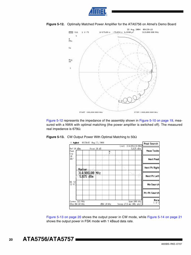
Figure 5-12. Optimally Matched Power Amplifier for the ATA5756 on Atmel's Demo Board
Figure 5-12 represents the impedance of the assembly shown in Figure 5-10 on page 19, mea-sured with a NWA with optimal matching (the power amplifier is switched off). The measuredreal impedance is 679Ω.
Figure 5-13. CW Output Power With Optimal Matching to 50Ω
Figure 5-13 on page 20 shows the output power in CW mode, while Figure 5-14 on page 21shows the output power in FSK mode with 1 kBaud data rate.
204835BS–RKE–07/07
ATA5756/ATA5757

ATA5756/ATA5757
Figure 5-14. FSK Output Power With Optimal Matching to 50Ω
The measured output power of the ATA5756 with 50Ω matching on the demo board is approxi-mately 5.7 dBm (Figure 5-13 on page 20 and Figure 5-14 on page 21). With the damping factorof the RF cable (about 0.5 dB), this corresponds to an output power of 6.2 dBm at the connector.
In FSK mode, the frequency deviation on Atmel's demo board is defined to be about ±35kHz.This is shown in Figure 5-15 on page 21.
Figure 5-15. Frequency Deviation of Atmel's Demo Board for ATA5756
214835BS–RKE–07/07
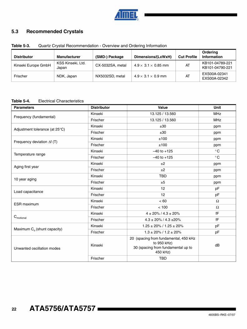
5.3 Recommended Crystals
Table 5-3. Quartz Crystal Recommendation - Overview and Ordering Information
Distributor Manufacturer (SMD-) Package Dimensions/(LxWxH) Cut ProfileOrdering Information
Kinseki Europe GmbHKSS Kinseki, Ltd. Japan
CX-5032SA, metal 4.9 × 3.1 × 0.85 mm ATKB101-04789-221KB101-04790-221
Frischer NDK, Japan NX5032SD, metal 4.9 × 3.1 × 0.9 mm ATEXS00A-02341EXS00A-02342
Table 5-4. Electrical Characteristics
Parameters Distributor Value Unit
Frequency (fundamental)Kinseki 13.125 / 13.560 MHz
Frischer 13.125 / 13.560 MHz
Adjustment tolerance (at 25°C)Kinseki ±30 ppm
Frischer ±30 ppm
Frequency deviation ∆f (T)Kinseki ±100 ppm
Frischer ±100 ppm
Temperature rangeKinseki –40 to +125 ° C
Frischer –40 to +125 ° C
Aging first yearKinseki ±2 ppm
Frischer ±2 ppm
10 year agingKinseki TBD ppm
Frischer ±5 ppm
Load capacitanceKinseki 12 pF
Frischer 12 pF
ESR maximumKinseki < 60 Ω
Frischer < 100 Ω
Cmotional
Kinseki 4 ± 20% / 4.3 ± 20% fF
Frischer 4.3 ± 20% / 4.3 ±20% fF
Maximum Co (shunt capacity) Kinseki 1.25 ± 20% / 1.25 ± 20% pF
Frischer 1.3 ± 20% / 1.2 ± 20% pF
Unwanted oscillation modesKinseki
20 (spacing from fundamental, 450 kHz to 950 kHz)
30 (spacing from fundamental up to 450 kHz)
dB
Frischer TBD
224835BS–RKE–07/07
ATA5756/ATA5757

ATA5756/ATA5757
6. Revision History
Table 5-5. Other Characteristics
Parameters Distributor Value Unit
Shock/bumpKinseki Suitable for TPMS
Frischer Suitable for TPMS
DropKinseki < ±20, suitable for TPMS
Frischer Suitable for TPMS
VibrationKinseki Suitable for TPMS
Frischer Suitable for TPMS
Centrifugal strength/accelerationKinseki < ±20, suitable for TPMS
Frischer Suitable for TPMS
Please note that the following page numbers referred to in this section refer to the specific revision mentioned, not to this document.
Revision No. History
4835BS-RKE-07/07
• Put application note in a new template
• Section 1 “Description” on page 1 changed• Section 5.2.1.1 “Output Matching to the Loop Antenna” on pages 14 to
15 changed• Table 4-1 “Bill of Materials (BOM)” on page 4 changed
234835BS–RKE–07/07

4835BS–RKE–07/07
Headquarters International
Atmel Corporation2325 Orchard ParkwaySan Jose, CA 95131USATel: 1(408) 441-0311Fax: 1(408) 487-2600
Atmel AsiaRoom 1219Chinachem Golden Plaza77 Mody Road TsimshatsuiEast KowloonHong KongTel: (852) 2721-9778Fax: (852) 2722-1369
Atmel EuropeLe Krebs8, Rue Jean-Pierre TimbaudBP 30978054 Saint-Quentin-en-Yvelines CedexFranceTel: (33) 1-30-60-70-00 Fax: (33) 1-30-60-71-11
Atmel Japan9F, Tonetsu Shinkawa Bldg.1-24-8 ShinkawaChuo-ku, Tokyo 104-0033JapanTel: (81) 3-3523-3551Fax: (81) 3-3523-7581
Product Contact
Web Sitewww.atmel.com
Technical [email protected]
Sales Contactwww.atmel.com/contacts
Literature Requestswww.atmel.com/literature
Disclaimer: The information in this document is provided in connection with Atmel products. No license, express or implied, by estoppel or otherwise, to anyintellectual property right is granted by this document or in connection with the sale of Atmel products. EXCEPT AS SET FORTH IN ATMEL’S TERMS AND CONDI-TIONS OF SALE LOCATED ON ATMEL’S WEB SITE, ATMEL ASSUMES NO LIABILITY WHATSOEVER AND DISCLAIMS ANY EXPRESS, IMPLIED OR STATUTORYWARRANTY RELATING TO ITS PRODUCTS INCLUDING, BUT NOT LIMITED TO, THE IMPLIED WARRANTY OF MERCHANTABILITY, FITNESS FOR A PARTICULARPURPOSE, OR NON-INFRINGEMENT. IN NO EVENT SHALL ATMEL BE LIABLE FOR ANY DIRECT, INDIRECT, CONSEQUENTIAL, PUNITIVE, SPECIAL OR INCIDEN-TAL DAMAGES (INCLUDING, WITHOUT LIMITATION, DAMAGES FOR LOSS OF PROFITS, BUSINESS INTERRUPTION, OR LOSS OF INFORMATION) ARISING OUT OFTHE USE OR INABILITY TO USE THIS DOCUMENT, EVEN IF ATMEL HAS BEEN ADVISED OF THE POSSIBILITY OF SUCH DAMAGES. Atmel makes norepresentations or warranties with respect to the accuracy or completeness of the contents of this document and reserves the right to make changes to specificationsand product descriptions at any time without notice. Atmel does not make any commitment to update the information contained herein. Unless specifically providedotherwise, Atmel products are not suitable for, and shall not be used in, automotive applications. Atmel’s products are not intended, authorized, or warranted for useas components in applications intended to support or sustain life.
© 2007 Atmel Corporation. All rights reserved. Atmel®, logo and combinations thereof, AVR® and others are registered trademarks or trade-marks of Atmel Corporation or its subsidiaries. Windows® is a registered trademark of Microsoft Corporation in the US and/or other countries.Other terms and product names may be trademarks of others.