reducing signal coupling and crosstalk in monolithic
TRANSCRIPT

REDUCING SIGNAL COUPLING AND CROSSTALK IN MONOLITHIC, MIXED-SIGNAL
INTEGRATED CIRCUITS
by
MATTHEW JOHN CLEWELL
B.S., Kansas State University, 2011
A THESIS
submitted in partial fulfillment of the requirements for the degree
MASTER OF SCIENCE
Department of Electrical Engineering
College of Engineering
KANSAS STATE UNIVERSITY
Manhattan, Kansas
2013
Approved by:
Major Professor
Dr. William B. Kuhn

Copyright
MATTHEW JOHN CLEWELL
2013
Abstract
Designers of mixed-signal systems must understand coupling mechanisms at the system, PC
board, package and integrated circuit levels to control crosstalk, and thereby minimize
degradation of system performance. This research examines coupling mechanisms in a RF-
targeted high-resistivity partially-depleted Silicon-on-Insulator (SOI) IC process and applying
similar coupling mitigation strategies from higher levels of design, proposes techniques to reduce
coupling between sub-circuits on-chip.
A series of test structures was fabricated with the goal of understanding and reducing the
electric and magnetic field coupling at frequencies up to C-Band. Electric field coupling through
the active-layer and substrate of the SOI wafer is compared for a variety of isolation methods
including use of deep-trench surrounds, blocking channel-stopper implant, blocking metal-fill
layers and using substrate contact guard-rings. Magnetic coupling is examined for on-chip
inductors utilizing counter-winding techniques, using metal shields above noisy circuits, and
through the relationship between separation and the coupling coefficient. Finally, coupling
between bond pads employing the most effective electric field isolation strategies is examined.
Lumped element circuit models are developed to show how different coupling mitigation
strategies perform. Major conclusions relative to substrate coupling are 1) substrates with
resistivity 1 𝑘Ω · cm or greater act largely as a high-K insulators at sufficiently high frequency,
2) compared to capacitive coupling paths through the substrate, coupling through metal-fill has
little effect and 3) the use of substrate contact guard-rings in multi-ground domain designs can
result in significant coupling between domains if proper isolation strategies such as the use of
deep-trench surrounds are not employed. The electric field coupling, in general, is strongly
dependent on the impedance of the active-layer and frequency, with isolation exceeding 80 dB
below 100 MHz and relatively high coupling values of 40 dB or more at upper S-band
frequencies, depending on the geometries and mitigation strategy used. Magnetic coupling was
found to be a strong function of circuit separation and the height of metal shields above the
circuits. Finally, bond pads utilizing substrate contact guard-rings resulted in the highest degree
of isolation and the lowest pad load capacitance of the methods tested.

Page | iv
Table of Contents
Table of Figures ............................................................................................................................ vii
Table of Tables .............................................................................................................................. xi
Acknowledgements ....................................................................................................................... xii
1. Introduction – Sources of Coupling in Real-World Systems .................................................. 1
1.1 System-Level Coupling .............................................................................................. 2
1.2 Board-Level Coupling ................................................................................................ 3
1.2.1 Multi-Layer PC Boards ....................................................................................... 3
1.2.2 Separating Ground Domains ............................................................................... 5
1.2.3 Bypass Capacitors ............................................................................................... 6
1.2.4 Vias and Other Interconnects .............................................................................. 6
1.3 Package-Level Coupling ............................................................................................. 7
1.3.1 Bond Wire Inductances ....................................................................................... 8
1.3.2 Through-Silicon Vias .......................................................................................... 8
1.4 Chip-Level Coupling .................................................................................................. 9
1.4.1 Top-Level Coupling ............................................................................................ 9
1.4.2 Coupling through the Silicon ............................................................................ 10
2. Coupling Mechanisms and Mitigation Techniques On-Chip ................................................ 11
2.1 Bulk-CMOS .............................................................................................................. 11
2.2 Silicon-on-Insulator .................................................................................................. 12
2.2.1 Thin-Film SOI ................................................................................................... 13
2.2.2 Thick-Film SOI ................................................................................................. 14
2.3 Process Features in Thick-Film SOI ......................................................................... 16
2.3.1 Substrate/Well Contacts .................................................................................... 18
2.3.2 Channel-Stopper Implant .................................................................................. 18
2.3.3 Deep-Trench Isolation ...................................................................................... 19
2.3.4 Metal-Fill Layers .............................................................................................. 19
2.4 Motivation ................................................................................................................. 21
3. Electric Field Coupling .......................................................................................................... 23
3.1 Electric Field Coupling Analysis in Thick-Film SOI ............................................... 24
Page | v
3.1.1 Coupling through the Substrate ........................................................................ 24
3.1.1.1 Coplanar Strips ............................................................................................. 27
3.1.2 2D Surface Coupling through the Silicon Active-Layer ................................... 31
3.1.3 Lumped Element Coupling Models .................................................................. 32
3.1.3.1 Methods to Reduce Coupling ....................................................................... 33
3.2 Experimental Array and Measurements .................................................................... 33
3.2.1 Blank Test Cell ................................................................................................. 34
3.2.2 Active-Layer Resistance Coupling ................................................................... 35
3.2.3 Active-Layer Coupling with Channel-Stopper Implant Blocked ..................... 36
3.2.4 Coupling with Deep-Trench Isolation Surrounds ............................................. 37
3.2.5 Deep-Trenches with Channel-Stopper Implant Present .................................... 38
3.2.6 Fill-Metal Coupling .......................................................................................... 39
3.2.6.1 Active-Layer Coupling with Fill-Metals Blocked ....................................... 39
3.2.6.2 Effects of Fill-Metal on Inter-Metal Coupling ............................................. 41
3.2.7 Active-Layer Coupling with Metal-1 Guard-Rings .......................................... 43
3.2.8 N+ Diffusion Structures .................................................................................... 44
3.2.9 Use of PTAP Guard-Rings with N+ Diffusions ............................................... 46
3.3 Future Work .............................................................................................................. 47
4. Magnetic Coupling ................................................................................................................ 49
4.1 Magnetic Coupling Analysis..................................................................................... 49
4.2 Experimental Structure and Measurements .............................................................. 53
4.3 Future Work .............................................................................................................. 58
5. Bond Pad Coupling ................................................................................................................ 61
5.1 Experimental Array and Measurements .................................................................... 62
5.1.1 Deep-Trench Grid ............................................................................................. 65
5.1.2 Inserting Ground Pad ........................................................................................ 65
5.1.3 PTAP Guard-Ring and Metal-1 Shield ............................................................. 65
5.2 Effect of Coupling Mitigation on Pad Load Capacitance ......................................... 66
5.3 Future Work .............................................................................................................. 66
6. Conclusion ............................................................................................................................. 69
6.1 Electric Field Coupling ............................................................................................. 69

Page | vi
6.1.1 Designs with Multiple Ground Domains .......................................................... 69
6.2 Magnetic Coupling.................................................................................................... 70
6.3 Bond Pads ................................................................................................................. 71
Appendix A - Spectrum Analyzer Data Acquisition with LabVIEW ........................................... 73
Appendix B - Documentation of Coupling ICs ............................................................................ 75
References ..................................................................................................................................... 81
Page | vii
Table of Figures
Figure 1.1 – Photograph of the Kansas State University Body Area Network Board [3]. ............. 1
Figure 1.2 – Example of multi-layer PC board with (a) analog circuits on the top side and (b)
digital on the back side. .......................................................................................................... 4
Figure 1.3 – Example of (a) bus-topology and (b) star-topology. .................................................. 4
Figure 1.4 – Feedback path through the power supply causing oscillation in high-gain amplifiers
[2]. ........................................................................................................................................... 5
Figure 1.5 – (a) Power supply filter decoupling techniques and (b) circuit model of a via. .......... 6
Figure 1.6 – Diagram of a coplanar waveguide structure. .............................................................. 7
Figure 1.7 – (a) Photograph of the KSU Micro-Transceiver Radio showing the bond wires in a
QFN style package. (b) Photograph of the bottom of the QFN package. ............................... 8
Figure 1.8 – Currents in counter-wound inductors. ........................................................................ 9
Figure 2.1 – Typical bulk-CMOS cross-section showing coupling paths. ................................... 11
Figure 2.2 – Diagram of the standard cell frame. ......................................................................... 12
Figure 2.3 – Thin-film SOI technologies, (a) silicon-on-sapphire and (b) buried-oxide. ............. 13
Figure 2.4 – Typical thick-film SOI cross-section........................................................................ 14
Figure 2.5 – Typical features found in thick-film SOI processes. ................................................ 17
Figure 2.6 – Diagram of a PTAP and NTAP in thick-film SOI. .................................................. 18
Figure 2.7 – (a) Photograph and (b) diagram of a deep-trench grid structure. ............................. 19
Figure 2.8 – Photograph showing two different metal-fill patterns. ............................................. 20
Figure 2.9 – KSU Mars Micro-Transceiver Radio top-level layout. ............................................ 21
Figure 2.10 – Enlarged layout view of analog and digital sections of the KSU Micro-Transceiver
Radio. .................................................................................................................................... 22
Figure 3.1 – Transmitter/receiver coupling structures. ................................................................. 23
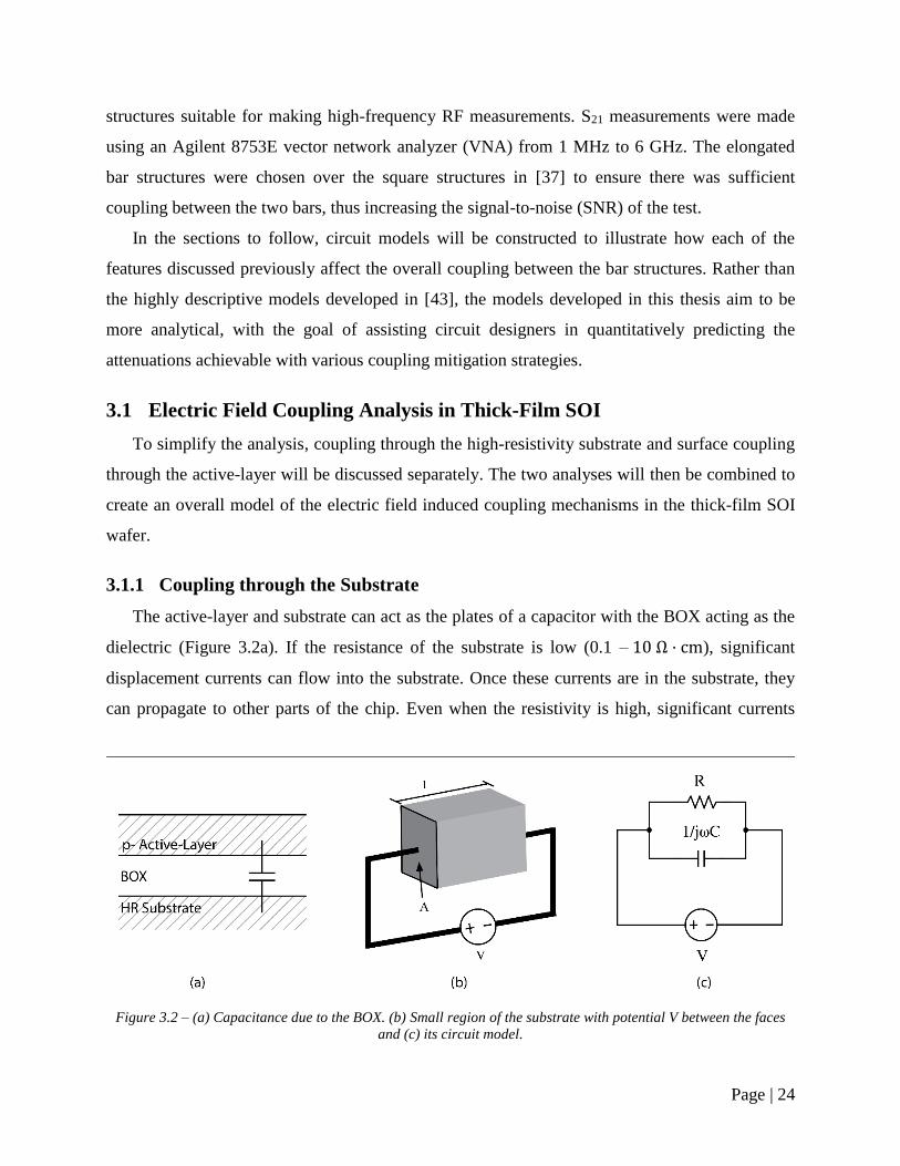
Figure 3.2 – (a) Capacitance due to the BOX. (b) Small region of the substrate with potential V
between the faces and (c) its circuit model. .......................................................................... 24
Figure 3.3 – Computed frequncies above which substrates behave more as a dielectric than a
conductor. .............................................................................................................................. 27
Figure 3.4 – Cross-section of coplanar strips................................................................................ 27

Page | viii
Figure 3.5 – (a) Capacitance per unit length for CPS versus spacing and (b) equivalent spacing of
a parallel plate capacitor for the same capacitance as CPS................................................... 29
Figure 3.6 – (a) ADS simulation schematic for the coupling between CPS for 10 µm spacing and
(b) simulated S21 for 5 μm wide, 100 μm long bars with 10 μm spacing (red) and 100 μm
spacing (blue). ....................................................................................................................... 30
Figure 3.7 – (a) Diffusion generator and receiver P+ bars in p- active-layer and (b) the simplified
lumped element circuit coupling model. (c) N+ diffusion generator and receiver bars in p-
active-layer and (d) the simplified lumped element circuit coupling model. ....................... 31
Figure 3.8 – (a) Die photo of fabricated electric field coupling test-structure array. (b) Example
generator/receiver structure with deep-trench isolation surrounds and metal-fill layers
blocked. ................................................................................................................................. 34
Figure 3.9 – (a) Layout of blank test cell and (b) measured S21 of the blank test cell. ................. 34
Figure 3.10 – Measured S21 for P+ diffusions in p- active-layer with 10 μm (red) and 100 μm
(blue) separations. ................................................................................................................. 35
Figure 3.11 – Measured S21 for P+ diffusions in p- active-layer with channel-stopper implant
blocked with 10 μm (red) and 100 μm (blue) separations. ................................................... 36
Figure 3.12 – Simplified circuit model for P+ bars in p- active-layer with addition of deep-trench
series capacitance. ................................................................................................................. 37
Figure 3.13 – Measured S21 for P+ diffusions in p- active-layer with deep trench surrounds and
channel-stopper implant blocked with 10 μm (red) and 100 μm (blue) separations. ........... 38
Figure 3.14 – Measured S21 for P+ diffusions in p- active-layer with deep trench surrounds with
10 μm (red) and 100 μm (blue) separations and channel-stopper present between the bars. 39
Figure 3.15 – (a) Diagram showing coupling path formed from metal-fill. (b) Measured S21 for
P+ diffusions in p- active-layer with (red) and without (blue) metal-fill layers blocked with
100 μm separation. ................................................................................................................ 40
Figure 3.16 – Measured S21 for P+ diffusions in p- active-layer with deep-trench surrounds and
channel-stopper blocked, with (red) and without (blue) the metal fill layers blocked, using
100 μm bar separation. .......................................................................................................... 40
Figure 3.17 – (a) Simplified diagram of the Metal-1 interdigitated planar capacitor and (b)
lumped element circuit coupling model. ............................................................................... 41

Page | ix
Figure 3.18 – Photograph of the interdigitated Metal-1 structures, (a) with metal-fill and (b)
without. ................................................................................................................................. 42
Figure 3.19 – Measured S21 of the interdigitated test structures in Figure 3.18 with (red) and
without (blue) metal-fill above the fingers. .......................................................................... 42
Figure 3.20 – Diagram of P+ diffusions in p- active-layer with Metal-1 guard-ring. .................. 43
Figure 3.21 – Measured S21 for P+ diffusions in p- active-layer with a metal-1 electrostatic
guard-ring (red) and without guard-ring (blue), with 10 μm separation (metal-fill and
channel-stopper implant are blocked). .................................................................................. 43
Figure 3.22 – Diagram of the NFET test structure showing grounded body-ties on either side of
the FETs. ............................................................................................................................... 44
Figure 3.23 – (a) Measured S21 for zero-biased NFETs with no coupling mitigation (red) and P+
diffusions in p- active-layer with deep trench surrounds (blue), using two 100/0.18 μm
NFETs with 10 μm separation. (b) Simulated S21 for the former case. ................................ 45
Figure 3.24 – Lumped element model for Figure 3.22, with body-ties represented as resistors to
ground. .................................................................................................................................. 45
Figure 3.25 – Measured S21 for biased NFETs with PTAP guard-ring surround (red) and P+
diffusion in p- active-layer with deep trench surround (blue), using 100/0.18 μm NFETs
with 10 μm separation. .......................................................................................................... 46
Figure 3.26 – Diagram of N+ diffusions in p- active-layer with PTAP guard-ring surrounds. .... 47
Figure 3.27 – Layout of new blank test cell with deep-trench grid under the signal pads (left) and
100/0.18 μm NFETs separated by 100 µm with PTAP guard-ring and deep-trench surrounds
(right). ................................................................................................................................... 48
Figure 4.1 – Model of the basic magnetic test structure consisting of a noise generator and an on-
chip planar spiral inductor..................................................................................................... 49
Figure 4.2 – (a) Mutually coupled generator and receiver inductors and (b) simplified circuit
model. .................................................................................................................................... 50
Figure 4.3 – Coupling coefficient versus inductor spacing (used with permission from [52]). ... 51
Figure 4.4 – Simulated S21 for two mutually coupled inductors while k is varied and (b)
simulated S21 with a fixed k and varying generator inductance. ........................................... 51
Figure 4.5 – Plot of the reduction of inductance in a single loop inductor due to metal shield
height. .................................................................................................................................... 53

Page | x
Figure 4.6 – (a) Photograph of fabricated magnetic test structure and (b) layout view of the
structure. ................................................................................................................................ 54
Figure 4.7 – Layout of a generator structure from Figure 4.6. ..................................................... 54
Figure 4.8 – (a) CMOS inverter switching characteristics and (b) schematic of the basic
generator structure showing currents and magnetic field lines. ............................................ 55
Figure 4.9 – Magnetic coupling without metal shield (top) and with metal shield (bottom). ...... 57
Figure 4.10 – Magnetic test structure with variable frequency noise generators. ........................ 59
Figure 4.11 – Current-starved VCO schematic............................................................................. 60
Figure 4.12 – Layout of current-starved VCO. ............................................................................. 60
Figure 5.1 – Photograph of the pad coupling test structure chip. ................................................. 62
Figure 5.2 –Diagram of the different bond pad coupling mitigation techniques. ......................... 63
Figure 5.3 – Bond pad coupling test structures showing the (a) 3-pad and (b) 4-pad variant
structures. .............................................................................................................................. 63
Figure 5.4 – Measured strength of the fundamental of the signal (1.5 GHz) coupled from the
generator pad to the receiver pad for both the 3-pad (left) and 4-pad test structures (right). 64
Figure 5.5 – Measured pad load capacitance with the coupling mitigation techniques applied. .. 66
Figure 5.6 – Diagram showing coupling path between bond pads through a floating VDD bus bar.
............................................................................................................................................... 67
Figure 5.7 – Layout of the new chip with updated pad coupling test structures. ......................... 68
Figure 6.1 – Coupling between ground domains when using substrate contact guard-rings (layout
top-view). .............................................................................................................................. 70
Figure 6.2 – Metal shield reducing electric field coupling. .......................................................... 71
Figure A.1 – Front panel view of the Spectrum Analyzer Data Acquisition LabVIEW Tool ..... 73
Figure A.2 – LabVIEW VI of the Spectrum Analyzer Data Acquisition LabVIEW Tool. .......... 74
Figure A.3 – LabVIEW VI to save a waveform as a text file in the CSV format. ....................... 74
Figure B.1 – Electric field coupling test chip layout. ................................................................... 75
Figure B.2 – Photograph of the electric field test array IC. .......................................................... 76
Figure B.3 – Magnetic and pad coupling test chip (Version 1). ................................................... 77
Figure B.4 – Photograph of the magnetic/pad coupling test IC (Version 1). ............................... 78
Figure B.5 – Magnetic and pad coupling test chip (Version 2). ................................................... 79
Page | xi
Table of Tables
Table 2.1 – Representative parameter values for a thick-film SOI process.................................. 17
Table 3.1 – Measured Ractive parameters for P+ diffusions in Figure 3.10. .................................. 35
Table 3.2 – Measured Ractive and Xc parameters for the P+ diffusions with the channel-stopper
implant blocked. .................................................................................................................... 36
Table 3.3 – Measured Xc values for the P+ diffusions with deep-trench surrounds extracted from
Figure 3.13. ........................................................................................................................... 38
Table 5.1 – Description of new pad coupling structures from Figure 5.7 .................................... 68
Table B.1 – Cell descriptions of the electric field coupling test chip array. ................................. 76

Page | xii
Acknowledgements
This work was supported in part by a research contract with Sandia National Laboratories.
Sandia National Laboratories is a multi-program laboratory managed and operated by Sandia
Corporation, a wholly owned subsidiary of Lockheed Martin Corporation, for the U.S.
Department of Energy’s National Nuclear Security Administration under contract DE-AC04-
94AL85000. Research was also supported under NASA EPSCoR Project NNX11AM05A.

Page | 1
1. Introduction – Sources of Coupling in Real-World Systems
Designers of mixed-signal integrated circuits need to understand coupling mechanisms to
control cross-talk between circuit blocks and thereby minimize the degradation of system
performance. The objective of this thesis is to provide IC designers with a guide to reduce
undesired coupling on-chip. Although this research primarily focuses on analog RF systems
designed in Silicon-on-Insulator (SOI) substrates, this work can be of use to any IC designer no
matter the frequency or substrate.
To illustrate some of the issues in a complex, mixed-signal system, the Kansas State
University Body Area Network (BAN) board will be used as an example [1]. A photograph of
this board is shown in Figure 1.1. The BAN board is designed to harvest energy from the
environment and using that energy, report biometric sensor data wirelessly to another radio. This
system contains a UHF radio, microcontroller (MCU), FPGA, and analog sensors on a
companion daughter board (not pictured). The UHF radio communication link is provided by the
KSU Micro-Transceiver [2]. This radio integrates a complete RF frontend including a
transmitter, receiver, M-PSK modulator, baseband IF and synthesizer on a single 9 mm2 chip.
Figure 1.1 – Photograph of the Kansas State University Body Area Network Board [3].
UHF Radio
EMI Shield
Ring
MCU
FPGA

Page | 2
1.1 System-Level Coupling
Before the in-depth analysis of coupling issues on-chip, circuit designers should note that
many of the same coupling issues that plaque the integrated circuit world are present in higher
levels of product design. Therefore it is beneficial to address some of the more common coupling
issues that are present at the various levels of product design and their mitigation strategies.
The first area to address coupling issues is at the system-level in the early design phases of a
product. Major architectural design decisions at this level can have a significant impact on
coupling, system performance and complexity. In the KSU radio, for instance, the choice of
whether to operate in full-duplex or half-duplex mode was a significant driver for the coupling
mitigation strategies employed later in the circuit design. If operating in full-duplex, the strong
signal from the transmitter could couple into the sensitive receiver and degrade performance,
whereas only operating in half-duplex mode, the transmitter is off during receive. The latter
mode was chosen to decrease system complexity and development time.
The type of power supplies and regulators employed is another important system-level
consideration. Switch-Mode Power Supplies (SMPS) are used for battery powered applications
due to their high efficiency. However to obtain high efficiency and small size, high-amplitude
energy must be switched at high frequencies. The electromagnetic interference (EMI) from the
switching frequency and its harmonics can couple into other circuit blocks in the same system or
even disrupt outside systems – in particular a nearby antenna. Due to the small form-factor of the
BAN board and the sensitive UHF radio, less efficient linear regulators were used.
One common technique to gain some immunity from noise sources such as SMPS is to use
differential signaling. In most situations, electric field induced EMI will couple onto both
signaling lines of the differential circuit equally. Due to the high common-mode rejection
characteristics of differential circuits, their noise immunity is much higher than single-ended
circuits. However, differential circuits may increase the complexity of designs and the static
power dissipation due to their Class-A nature. Differential signaling is not just limited to the
system-level – most of the sensitive RF sections on the KSU radio are differential.
Formulating a frequency plan to identify critical system frequencies and bandwidths is
another important technique in high performance mixed-signal systems. Clocks from devices
such as MCUs and FGPAs can generate numerous harmonics over a wide range of frequencies
that can couple into sensitive subs-systems. Identifying critical bandwidths and choosing clock
Page | 3
frequencies to avoid in-band interference can decrease complexity and increase performance by
not requiring sub-systems to filter intra-system interferers. For example, if a SMPS is used in
conjunction with an audio sub-system, selecting the switching frequency outside the range of
human hearing can minimize undesired signals from falling in the audio band. On the BAN
board, the clocks for the MCU, FPGA and synthesizer reference were chosen to prevent their
harmonics from falling close to a desired receive channel or image frequency of the receiver.
Other important considerations the frequency plan should include are loop bandwidths of
synthesizers and IF bandwidths in receivers. If the system is to operate in an environment with
strong external interferes, such as those from the cellular and ISM bands, these frequencies must
also be addressed.
1.2 Board-Level Coupling
The next level where coupling issues should be addressed is the PC board-level. Perhaps the
most well studied level, designers recognize early on the potential for coupling problems,
especially in mixed-signed environments. Digital logic families such as TTL and CMOS have
large switching currents that can produce significant amounts of EMI. Other digital circuitry on
the PC board may be immune due to their high noise margins; however analog circuitry does not
usually have this luxury.
1.2.1 Multi-Layer PC Boards
One effective way to isolate digital and analog circuit blocks is to use a multi-layer PC board.
With a four-layer board, for instance, digital circuits can be routed on the top layer and analog
circuits on the bottom, such as shown in the commercially designed cell-phone PC board in
Figure 1.2. Within the board itself, the two inner layers then can be used for power and ground.
The power and ground planes act similar to an EMI shield, reducing the coupling between the
top and bottom signal layers. In an ideal situation, each signal layer would be buried between
two ground planes to form a coaxial cable like structure called stripline [4]. However, this
increases the cost and complexity of the PC board and is usually unnecessary. For example, the
BAN board shown previously in Figure 1.1 contains a high gate-count FPGA together with a
UHF receiver operating to levels as low as -120 dBm (0.22 µV into 50 Ω) with a four layer
board on which both analog/RF and digital circuits co-located on the top layer, with a solid

Page | 4
ground plane 12 mil below. Successful operation is achieved thanks to careful routing at the PC
board-level and frequency planning at the system-level.
If further EMI mitigation is needed, grounded metal shielding structures can be soldered
directly to the board (also present on the PC board in Figure 1.2). On the BAN board in Figure
1.1, a ring of copper was left exposed to attach an optional EMI shield. Stitching vias can be seen
along the ring to create a low impedance path to ground. This optional shield may be used when
this board is combined with a daughter board which forms a capacitively loaded top hat antenna
[5], since the antenna represents a much more vulnerable component in the system if it is to be
operated in receive-mode.
With a more limited number of layers in the PC board, an effective way to isolate circuit
blocks is to keep the analog and digital supply and ground currents separate. In Figure 1.3a, the
sensitive analog circuit can be seen connected to noisy digital circuit blocks using a bus
topology. The strong switching currents the digital blocks draw from the power supply can
Figure 1.2 – Example of multi-layer PC board with (a) analog circuits on the top side and (b) digital on the back
side.
Figure 1.3 – Example of (a) bus-topology and (b) star-topology.
EMI
Shield

Page | 5
induce ripple on the supply voltage due to the non-ideal nature of the power supply and the non-
zero impedances in the power supply trace on the PC board.
1.2.2 Separating Ground Domains
A good approach for connecting the grounds of circuit blocks in a limited two layer PC
board environment may be to use the star-topology shown in Figure 1.3b. An even more ideal
approach is to use the star-topology for both the power and ground rails [6], [7]. However, in
complex designs this may be unfeasible. As shown in Figure 1.3b, each of the three circuit
blocks has an individual connection to the return on the power supply. This could also be
realized on a 4-layer circuit board by providing individual subdivided ground planes for each of
the digital and analog circuit blocks (denoted with the different ground symbols in Figure 1.3b).
Each of the grounds domains will then need to connect to the return of the power supply at some
point on the PC board. Care must be taken to ensure that this point does not cause the ground
domains to interact. For this reason, a single, unbroken ground plane is more typically used [8].
Coupling between circuit blocks in the same ground domain can also occur due to feedback
in the power-supply rails. Take for example the case of a series of cascaded amplifiers shown in
Figure 1.4. The last amplifier will pull strong currents from the power supply and can cause
voltage ripples to appear on the power supply rail. The now modulating power supply rail can
produce a signal at the amplifier input. This ripple will then be amplified by the first amplifier.
The amplified ripple is then amplified by the next stage which is also amplifying the ripple seen
on the power supply. This then continues through the chain of amplifiers, eventually causing it to
oscillate if the loop-gain is sufficiently high. The solution to this problem is to employ bypass
capacitors as shown.
Figure 1.4 – Feedback path through the power supply causing oscillation in high-gain amplifiers [2].
Page | 6
1.2.3 Bypass Capacitors
Adding bypass (decoupling) capacitors is one common – and necessary – method to reduce
the feedback issues caused by signals injected onto the power supply rail. The signal injection is
reduced by providing the signals with a low impedance path to ground through the bypass cap.
As the clock frequencies of designs increases, the parasitic properties of the bypass capacitors
must also be taken into account. As the frequency increases above the self-resonant frequency
(SRF), the capacitor will begin to act more and more like an inductor [9], limiting its ability to
create the desired AC path to ground. Care must to taken to ensure proper capacitors with
sufficiently high SRFs and sufficiently short interconnects are used in high frequency designs.
In conjunction with bypass capacitors, further power supply isolation can be achieved by
placing an inductor in series with the power supply (Figure 1.5a). If a SMD inductor is used, the
response of the LC filter combined with the supply source impedance can result in resonances
and very poor bypassing at select frequencies. A resistor can be placed in series to lower the
quality-factor of the LC resonator (“de-Q it”), however the resistance must be kept small to
minimize IR drops. Alternatively, a ferrite bead could be used. At low frequencies (<100 KHz)
they act as inductors. However, at high frequencies ferrites beads are very resistive [10]. Hence
they pass the DC supply current while blocking signal currents, as desired.
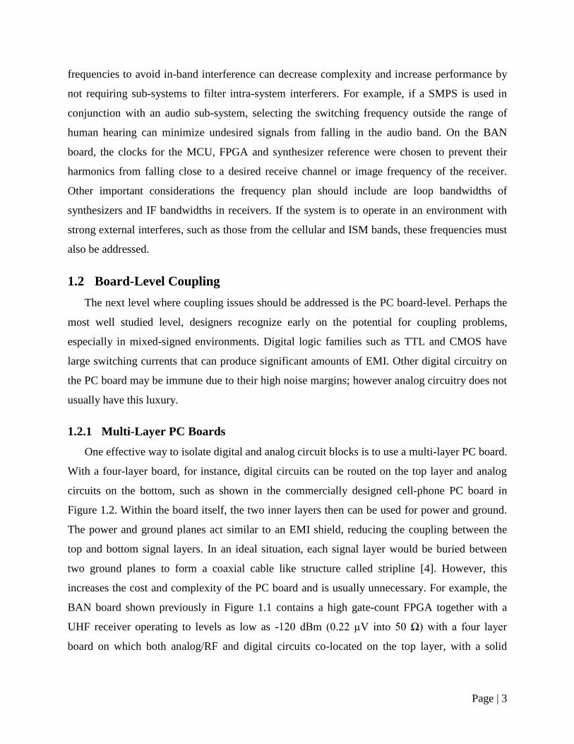
1.2.4 Vias and Other Interconnects
One final issue board-level designers must consider is the parasitic nature of vias and other
interconnects on PC boards. An equivalent lumped element circuit model of a via is shown in
Figure 1.5b [11]. The non-ideal nature of vias can create discontinuities in microwave structures
Figure 1.5 – (a) Power supply filter decoupling techniques and (b) circuit model of a via.

Page | 7
such as microstrip and stripline which can degrade RF performance. Moreover, the inductance
inherent in vias create non-negligible impedances at RF frequencies between the ground pins of
IC packages or bypass capacitors and the ground node on a PC board. Currents flowing through
these impedances create “ground-bounce” voltages. Just as before, the ground-bounce can cause
feedback and oscillation. One way to reduce this effect is to reduce the inductance in the via.
This can be done by physical shrinking the length of the via by using thinner PC boards. Another
simple way to reduce the inductance is to use multiple vias for ground. This effectively makes
the via inductances appear in parallel, reducing the overall inductance seen by a circuit node.
This technique necessarily causes the associated ground conductors on the surface of the board to
become larger and the ground is effectively moved to the surface. The resulting surface artwork
then takes on a form of a coplanar waveguide (CPW) structure (Figure 1.6), which can allow
operation well into the microwave and millimeter wave bands [12].
1.3 Package-Level Coupling
Another source of ground-bounce is the package used to mount the integrated circuit to the
PC board. The pins from the package to the PC board and associated bond wires within the
package also contribute to total parasitic inductance seen by the integrated circuit and must be
taken into account when considering high-frequency analog or high-speed digital designs. Bulky
DIP (dual-inline package) style packages with long pins have been replaced with slimmer gull-
wing type surface-mount packages such as QFP (quad-flat package). For even higher speed
designs, lead-less QFN (quad-flat, no-leads) style packages are becoming the norm. BGA (ball-
grid array) style packages are often used for very high pin count ICs such as processors and
memory. For high performance RF designs, the IC can be flipped over and soldered directly to
the PCB in a processed called flip-chip [13]. All of these different packaging technologies strive
to reduce the length of the leads and thus the parasitic inductance.
Figure 1.6 – Diagram of a coplanar waveguide structure.

Page | 8
1.3.1 Bond Wire Inductances
If using a package technology that requires wire bonding, the inductance of the bond wires
must be considered. Typical bond wire inductances are on the order of 1 nH/mm and just like
vias on a PC board, present non-negligible impedances at RF frequencies. The KSU radio shown
in Figure 1.7a is mounted inside a QFN package with an exposed ground pad (Figure 1.7b). A
series of vias connect the exposed ground pad to the ground plane below the IC on the BAN
board of Figure 1.1 to create a low impedance ground. The chip is bonded to the package paddle
(gold surface in Figure 1.7a) which is directly connected to the exposed ground pad on the
bottom of the package. To reduce the length of the bond wires connecting the grounds of the IC,
they can be “down-bonded” directly to the paddle instead of to the lead frame of the QFN
package. By using down-bonds, the bond wire length and therefore its inductance can be cut in
half. As with vias, if even lower inductance is needed, multiple pins in parallel may be used as
ground returns.
1.3.2 Through-Silicon Vias
If the integrated circuit process supports back-of-the-wafer metallization, through-silicon vias
(TSV) can be used to connect the on-chip grounds directly to the paddle [14]. Similar to vias on
a PCB board, TSVs allow a connection from the metal layers on the top of the IC to the backside
of the wafer. Depending on the thickness of the wafer, TSVs have the potential to reduce the
ground inductance even further than using down-bonds. The drawback is that they consume large
Figure 1.7 – (a) Photograph of the KSU Micro-Transceiver Radio showing the bond wires in a QFN style
package. (b) Photograph of the bottom of the QFN package.
Down-Bond Exposed
ground pad

Page | 9
areas on chip, require extra processing and increase the cost of the wafer. Common processes
that support TSVs are GaAs and SiGe where microwave and millimeter wave operation is
targeted.
1.4 Chip-Level Coupling
The final level at which coupling analysis should be performed and the focus of this thesis is
the chip-level. Many of the same coupling mitigation techniques used in the previous levels of
design are useful when attempting to address the issues of on-chip coupling. Similar to PC
boards, both internal and external signals can couple into sensitive sub-circuits and degrade
performance. As with the previous discussion, coupling mitigation on-chip can be broken into
top-level and silicon-level strategies.
1.4.1 Top-Level Coupling
The use of differential circuits is critical for noise immunity from both internal and external
signal sources. The KSU radio makes extensive use of differential circuit topologies in sub-
circuits such as the LNA, mixer, IF amplifiers, VCO and modulator [2]. EMI shields can be
realized on-chip by placing metal floods over noisy circuit blocks. In [15] a thin magnetic film of
CoZrNb applied to magnetically noisy circuits showed improvements in reducing coupling.
However, this technique is outside the features offered by typical commercial processes. In [16]
magnetic shields to reduce coupling between adjacent traces are proposed. In the KSU radio, a
grounded metal flood was placed over the noisy digital synthesizer to reduce the amount of
Figure 1.8 – Currents in counter-wound inductors.

Page | 10
magnetic coupling into the sensitive receiver.
Further EMI suppression can be obtained by counter-winding on-chip spiral inductors in
differential circuits such as LNAs and VCOs [2]. Figure 1.8 shows the relationship of the
windings of the inductors in the PA and VCO of the KSU radio. The strong currents in the PA
inductor can couple magnetically (and to a lesser extent through electric field lines) into the
VCO. These currents could potentially pull the phase of the VCO and corrupt the transmitted M-
PSK signal constellation or even prevent the synthesizer from locking the VCO. The current
labeled 𝑖𝑣𝑐𝑜 in Figure 1.8 represents the nominal oscillation current of the VCO. The magnetic
field from the PA inductor will induce a voltage and hence a current 𝑖𝑖𝑛𝑑 in the inductors of the
VCO. Since the VCO inductors are positioned on the center-line of the PA inductor, the induced
currents should couple equally onto each of the VCO inductors. The induced currents will flow
through the inductors in opposite directions and cancel. Furthermore, the current 𝑖𝑣𝑐𝑜 in the
counter-wound VCO inductors produces a zero net magnetic field outside the two inductors, at
least along the dotted centerline shown. This has the added benefit of reducing the amount of
coupling from the VCO to other parts of the radio, such as the LNA in the receiver.
Chip designers must also be aware of ground-bounce issues at the chip-level. The high sheet-
resistances of the metals due to small geometries in semiconductors can result in significant IR-
drops. Wide metals therefore should be used to ensure low impedance power and ground paths.
Due to the inductance of bond wires, further on-chip decoupling should be provided to form
solid AC grounds where possible. Another way to combat supply noise is to use active RC filters
on the supply lines such as those used on KSU radio in [2]. These supply filters in conjunction
with the off-chip bypass capacitors on the supply attenuate signals on the power supply rails in
the high-gain IF amplifier subsection of the radio to prevent oscillation.
1.4.2 Coupling through the Silicon
Unlike the thick, insulative materials typically used in PC boards, the semiconducting
substrate used in most ICs has the potential for many non-ideal coupling situations. This causes
the coupling analysis in processes such as bulk-CMOS and SOI to be much more complicated
than PC board level coupling issues. In the following chapters, the various coupling mechanisms
on-chip will be explored along with their different coupling mitigation strategies.
Page | 11
2. Coupling Mechanisms and Mitigation Techniques On-Chip
Over the history of integrated circuits, many different wafer technologies have been
developed for various applications. However, the primary driving force behind these new
technologies has been integration. To achieve this goal, mixed-signal sub-systems that were once
separate, such as receivers, transmitters and synthesizers, are being incorporated on the same
physical die. To allow IC designers to build more highly integrated chips, the coupling
mechanisms and mitigation strategies must be well understood. This research focuses on
characterizing the coupling mechanisms and formulating mitigation strategies to reduce coupling
in a relatively new IC design process type: partially-depleted silicon-on-insulator (SOI).
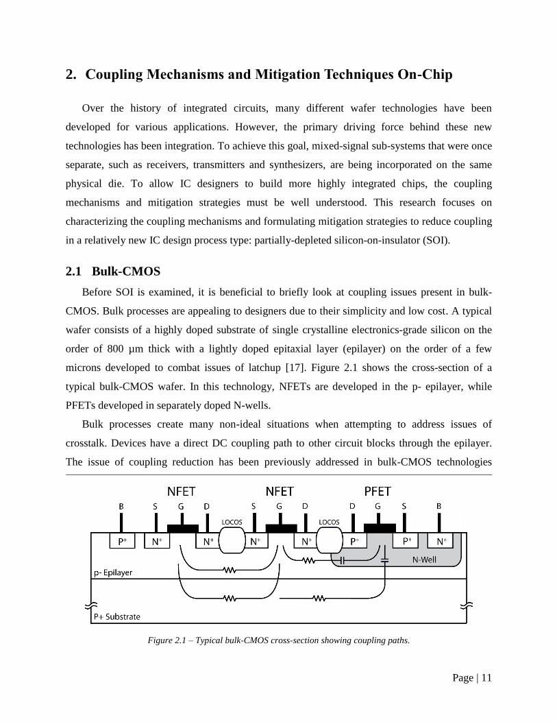
2.1 Bulk-CMOS
Before SOI is examined, it is beneficial to briefly look at coupling issues present in bulk-
CMOS. Bulk processes are appealing to designers due to their simplicity and low cost. A typical
wafer consists of a highly doped substrate of single crystalline electronics-grade silicon on the
order of 800 µm thick with a lightly doped epitaxial layer (epilayer) on the order of a few
microns developed to combat issues of latchup [17]. Figure 2.1 shows the cross-section of a
typical bulk-CMOS wafer. In this technology, NFETs are developed in the p- epilayer, while
PFETs developed in separately doped N-wells.
Bulk processes create many non-ideal situations when attempting to address issues of
crosstalk. Devices have a direct DC coupling path to other circuit blocks through the epilayer.
The issue of coupling reduction has been previously addressed in bulk-CMOS technologies
Figure 2.1 – Typical bulk-CMOS cross-section showing coupling paths.

Page | 12
through the use of LOCOS (local oxidation of silicon [18]), STI (shallow-trench isolation [19]),
guard-rings, buried layers and differential circuits [20]–[23]. LOCOS, STI, and guard-rings can
be effective at reducing the coupling through the lightly doped epilayer. However, they are
ineffective at reducing coupling for signals injected into the highly doped P+ substrate which
creates a low impedance coupling path between active devices [20]. Due the effectiveness of this
coupling path once signals are injected into the substrate they can couple into circuitry a great
distance from the source. Buried layers and triple-well processes [24] can be used to reduce
deep-substrate coupling, however they increase the wafer cost.
The junction capacitance between N-wells and the p- epilayer can also be used to reduce
surface coupling. Lower frequency signals can be contained in their respective wells by keeping
P devices in a continuous n-well and N devices in a continuous p-well, as shown in Figure 2.2.
Power and ground rails can be routed on the top and bottom and substrate contact guard-rings
can be added for isolation. This method of routing is called the standard cell-frame [25] and is
widely used in bulk-CMOS and other wafer technologies to improve auto-routing in VLSI
algorithms and to reduce the effects of latchup. This technique is also referred to as the line-of-
diffusion, recognizing the long, continuous strips of n-well and p-well.
2.2 Silicon-on-Insulator
Silicon-on-Insulator (SOI) technologies attempt to address some of the major challenges of
bulk-CMOS – namely increasing device speed and reducing power consumption [26]. In these
technologies, a thin layer of silicon is grown on an insulating material, such as sapphire or SiO2,
backed with a silicon "handle" wafer. In fact, the first patented transistor was fabricated using
Figure 2.2 – Diagram of the standard cell frame.
Page | 13
SOI by J. E. Lilienfield in 1926 [27]. Though the technology in Lilienfield’s time was not
developed enough to successfully create his transistor, today there are many different foundries
manufacturing many different types of SOI. These wafers can be broken into two main
categories based on the thickness of the top layer of silicon: thin-film and thick-film.
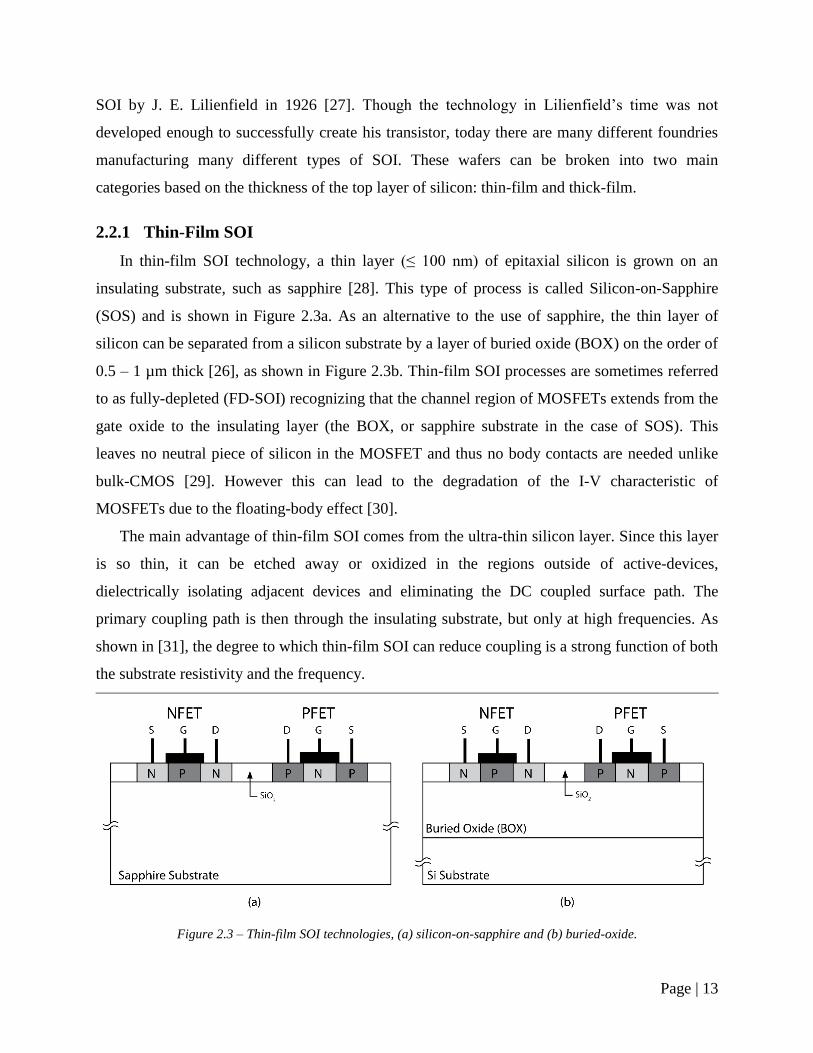
2.2.1 Thin-Film SOI
In thin-film SOI technology, a thin layer (≤ 100 nm) of epitaxial silicon is grown on an
insulating substrate, such as sapphire [28]. This type of process is called Silicon-on-Sapphire
(SOS) and is shown in Figure 2.3a. As an alternative to the use of sapphire, the thin layer of
silicon can be separated from a silicon substrate by a layer of buried oxide (BOX) on the order of
0.5 – 1 µm thick [26], as shown in Figure 2.3b. Thin-film SOI processes are sometimes referred
to as fully-depleted (FD-SOI) recognizing that the channel region of MOSFETs extends from the
gate oxide to the insulating layer (the BOX, or sapphire substrate in the case of SOS). This
leaves no neutral piece of silicon in the MOSFET and thus no body contacts are needed unlike
bulk-CMOS [29]. However this can lead to the degradation of the I-V characteristic of
MOSFETs due to the floating-body effect [30].
The main advantage of thin-film SOI comes from the ultra-thin silicon layer. Since this layer
is so thin, it can be etched away or oxidized in the regions outside of active-devices,
dielectrically isolating adjacent devices and eliminating the DC coupled surface path. The
primary coupling path is then through the insulating substrate, but only at high frequencies. As
shown in [31], the degree to which thin-film SOI can reduce coupling is a strong function of both
the substrate resistivity and the frequency.
Figure 2.3 – Thin-film SOI technologies, (a) silicon-on-sapphire and (b) buried-oxide.

Page | 14
2.2.2 Thick-Film SOI
In thick-film SOI processes, a much thicker layer of silicon on the order of 1 µm sits above
an insulating layer such as SiO2 (Figure 2.4). Unlike thin-film technologies, the channels of
thick-film MOSFETs do not extend to the BOX layer and thus are alternatively referred to as
partially-depleted SOI (PD-SOI). Since there is neutral silicon under the channels regions of
MOSFETs, body contacts are required and when used, the floating-body effect is not present.
Due to the lack of surface isolation, the coupling mechanisms are much more complicated to
analyze and more resemble those of bulk-CMOS technologies. However, if the process supports
deep-trenches [26], surface coupling can be reduced and the coupling properties can become
closer to that of the more ideal thin-film case. As shown in Figure 2.4, a deep-trench of SiO2 can
extend from the surface of the top silicon active-layer down to the BOX. Surrounding an entire
transistor with a deep-trench will result in complete surface dielectric isolation. However like
guard-rings in bulk-CMOS, deep-trenches are ineffective against signals coupled into the
substrate. Furthermore, surrounding active-devices with deep-trenches consumes large areas on-
chip and may not be practical for high density designs.
Other coupling mitigation techniques in thick-film SOI have also been explored such as
burying a conductive ground plane under the BOX, called ground-plane SOI (GPSOI) [32].
Although GPSOI can provide high isolation, the added step in manufacturing increases the cost
of the wafer. It is also well known that placing a ground plane under spiral planar inductors will
Figure 2.4 – Typical thick-film SOI cross-section.
Page | 15
severely degrade their performance, which is counter-productive to RF applications where high
quality-factor (high-Q) inductors are greatly desired.
Since SOI technologies are still evolving, fewer studies about coupling reduction have been
performed. Early investigations in [31] and [33] showed that SOI can have advantages over bulk-
CMOS from a coupling perspective, at least at lower frequencies. It has also been shown,
however, that a bulk-CMOS process with well-developed coupling mitigation strategies can
sometimes outperform SOI [34]. Studies in SOI such as [35] and [36] approached the issue of
coupling by modifying process specific parameters such as the thickness and depth of the BOX
and the resistivity of the handle substrate. In contrast, for the current thesis, only parameters that
are available to the designer will be modified such as increasing the spacing of circuits or adding
deep-trench. Following the techniques used in [37], the issue of coupling reduction in this
research will be focused on a typical high-resistivity SOI process that is commercially available
to the public.
Designs utilizing on-chip inductors, can experience not only coupling through the wafer but
also magnetic coupling through the metal layers. Magnetic coupling could occur between
inductors and/or circuits with ground loops. Though not necessarily specific to thick-film SOI,
magnetic coupling is also addressed in this thesis. Following the example in [16], a magnetic
isolation technique is examined over a wide range of frequencies.
Page | 16
2.3 Process Features in Thick-Film SOI
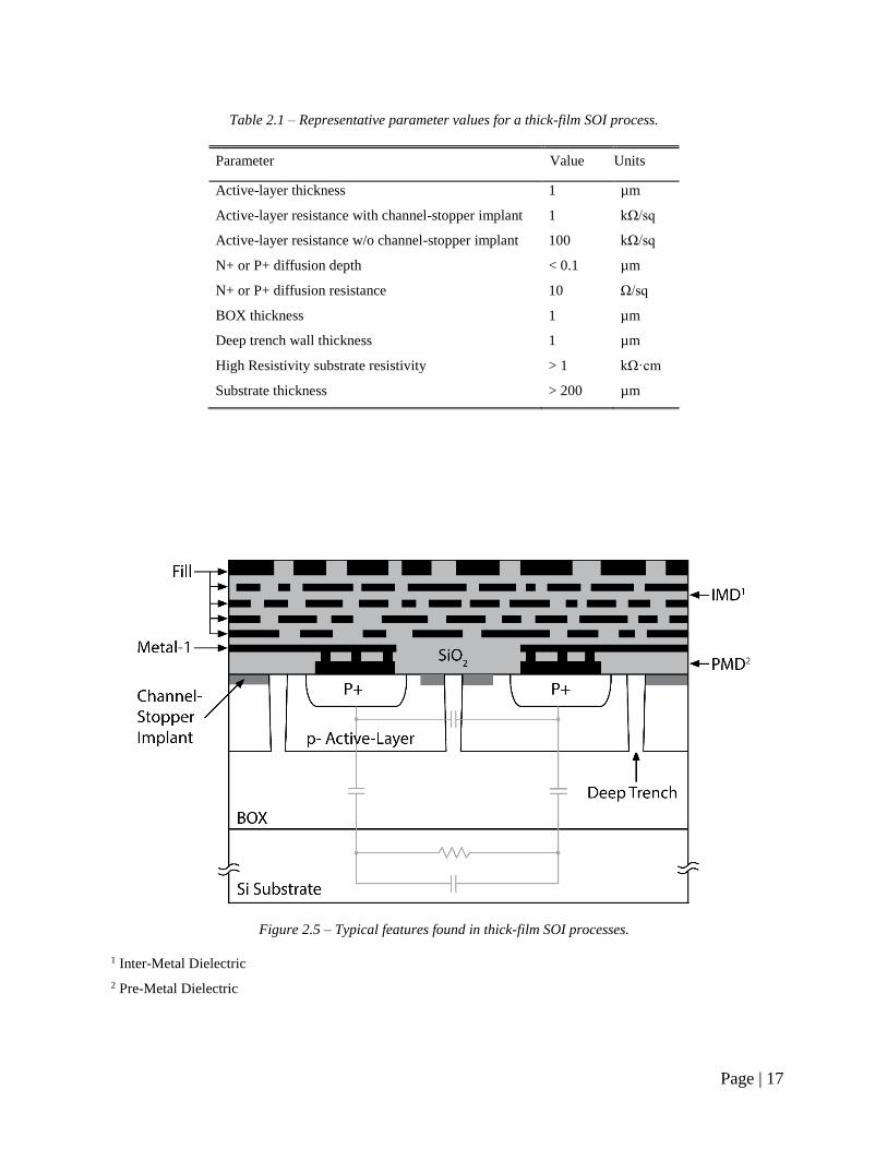
The primary focus of this research are thick-film SOI processes with a high-resistivity
substrate on the order of 1 𝑘Ω · cm. To characterize the coupling, various test structures were
designed and measured in a commercial SOI process with high-resistivity substrate targeted at
RF and mixed-signal designs. To protect the intellectual property rights of the fabrication
vendor, actual process specific parameters cannot be published. However, the values in Table 2.1
can be considered a good representation of a typical high-resistivity thick-film SOI process such
as that used in this research. A detailed cross-section showing different coupling paths in the
thick-film SOI is shown in Figure 2.5. This figure also illustrates some of the different features
that can be used to address the issue of cross-talk reduction in thick-film SOI. Layout issues
using this SOI process that were investigated are:
signal coupling through the high-resistivity substrate,
increasing the separation between circuits,
adding deep-trenches,
blocking the implant of channel-stopper,
blocking the dummy metal fill,
PTAP guard rings surrounds,
grounded Metal-1 guard-ring surrounds and
placing a Metal-1 shield over magnetically noisy circuits.
Page | 17
Table 2.1 – Representative parameter values for a thick-film SOI process.
Parameter Value Units
Active-layer thickness 1 µm
Active-layer resistance with channel-stopper implant 1 kΩ/sq
Active-layer resistance w/o channel-stopper implant 100 kΩ/sq
N+ or P+ diffusion depth < 0.1 µm
N+ or P+ diffusion resistance 10 Ω/sq
BOX thickness 1 µm
Deep trench wall thickness 1 µm
High Resistivity substrate resistivity > 1 kΩ·cm
Substrate thickness > 200 µm
Figure 2.5 – Typical features found in thick-film SOI processes.
1 Inter-Metal Dielectric
2 Pre-Metal Dielectric

Page | 18
2.3.1 Substrate/Well Contacts
Substrate contacts are highly doped diffusions of P+ into the p- active-layer (PTAP) or N+
into an N-doped well (NTAP). Figure 2.6 shows an example of a PTAP and an NTAP in thick-
film SOI. Unlike the rectifying contacts of the source and drain diffusions in MOSFETs, these
contacts are ohmic and do not form a depletion region. In processes such as bulk-CMOS and
thick-film SOI they are used to make the body connection to bias the active-layer. Rings of
substrate contacts, called guard-rings, can be placed around NMOS and PMOS devices to help
reduce the effects of latchup in a bulk-CMOS environment by collecting minority carriers in the
active-layer before they can reach the underlying substrate and propagate [38]. In a similar
fashion, substrate contact guard-rings can also be placed around sensitive circuitry to shunt
currents in the active-layer to ground and minimize coupling between circuits. This is possible in
both bulk-CMOS and in SOI. Due to the resistance and thickness of the active-layer, such
substrate contacts must be kept within a few microns of devices to be effective.
2.3.2 Channel-Stopper Implant
The channel-stopper implant is a shallow, high density P+ implant into the surface of the p-
active-layer, placed outside the active regions of devices such as MOSFETs and diodes. The
channel-stopper implant is also referred to as the field-implant, recognizing the area outside the
active regions on-chip is called the “field.” Its primary purpose is to prevent surface inversion
due to high voltage signal runs on metal layers above the active-layer. Voltages as high as 15V
can still be found in modern “low-voltage” processes in circuits such as high performance power
amplifiers. High voltages can cause the surface to invert from P to N creating a channel of low
Figure 2.6 – Diagram of a PTAP and NTAP in thick-film SOI.

Page | 19
resistance N type material under the high-voltage run, similar to the gate of a MOSFET. Signals
finding their way into this channel can couple into circuitry a great distance from the source.
Unfortunately, the P+ channel-stopper implant itself decreases the resistance of the active-layer,
forming a potentially strong surface coupling path for any signals that make their way into the
field areas – possibly through capacitive mechanisms.
2.3.3 Deep-Trench Isolation
As discussed previously, completely surrounding an active device with deep-trench
dielectrically isolates it from the rest of the active-layer. This results in no DC coupling path in
the active-layer and coupling properties can approach the case of thin-film SOI. Grid patterns of
deep-trench can also be used to effectively remove large areas of the active-layer. This is
especially useful for improving the Q of planar spiral inductors [39]. The bond pad in Figure 2.7a
employs a deep-trench grid underneath to reduce signals in the active-layer/substrate coupling
into the pad. As shown in the diagram in Figure 2.7b, islands of silicon from the active-layer will
still remain. As demonstrated in [39], if the grid geometries are similar in dimension to the DT
wall thickness, then these silicon islands will not have a large effect and the gridded area can be
considered largely insulating.
2.3.4 Metal-Fill Layers
In processes with multiple layers of routing metals, dummy metal may be added in the field
of the chip to increase the metal density in those areas. Metal-fill is added to minimize large
variations in the wafer surface topology [40], [41], which could result in undesired partial
(a) (b)
Figure 2.7 – (a) Photograph and (b) diagram of a deep-trench grid structure.

Page | 20
removal of portions of metal layers during chemical-mechanical polishing (CMP), leading to
open circuits. The metal-fill pattern varies by process, but in general consists of an array of metal
shapes, such as shown in Figure 2.8. On the left, automatically generated Metal-6 fill shapes can
be seen (metal-fill is present on the lower metal layers, but is obfuscated by the Metal-6 fill). On
the right, a custom high-density metal-fill was used to further increase the metal density in that
area. Fill patterning may also be done on the poly-silicon layers used for the gates of MOSFETs.
The field of the chip may also be doped with “active fill” shapes to control the variance of
breakdown voltages of active devices [42].
Figure 2.8 – Photograph showing two different metal-fill patterns.
Page | 21
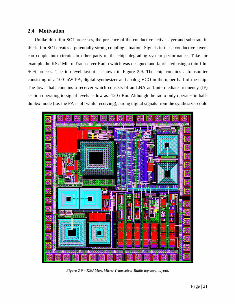
2.4 Motivation
Unlike thin-film SOI processes, the presence of the conductive active-layer and substrate in
thick-film SOI creates a potentially strong coupling situation. Signals in these conductive layers
can couple into circuits in other parts of the chip, degrading system performance. Take for
example the KSU Micro-Transceiver Radio which was designed and fabricated using a thin-film
SOS process. The top-level layout is shown in Figure 2.9. The chip contains a transmitter
consisting of a 100 mW PA, digital synthesizer and analog VCO in the upper half of the chip.
The lower half contains a receiver which consists of an LNA and intermediate-frequency (IF)
section operating to signal levels as low as -120 dBm. Although the radio only operates in half-
duplex mode (i.e. the PA is off while receiving), strong digital signals from the synthesizer could
Figure 2.9 – KSU Mars Micro-Transceiver Radio top-level layout.

Page | 22
couple into the sensitive analog LNA and IF sections. Successful operation was achieved in thin-
film SOS due to careful layout, the use of differential circuitry and frequency planning.
Additionally, a grounded metal-shield was placed over the digital synthesizer to reduce coupling
to other parts of the radio.
However, if the thin-film SOS radio design were ported to a thick-film SOI process without
addressing thick-film specific coupling issues, the performance of the radio could be
substantially degraded. One of the many locations where coupling issues could arise is through
the physical proximity between the analog IF section and digital circuitry in the synthesizer. An
enlarged view of this region is shown in Figure 2.10, showing the digital synthesizer circuitry in
the top and the analog IF circuitry in the bottom. The active-layer and high-resistivity substrate
could allow strong digital signals from the synthesizer to couple into the sensitive analog IF
section.
In the chapter to follow, electric field coupling mechanisms in thick-film SOI will be
analyzed. In later chapters, magnetic coupling and bond pad coupling will also be investigated.
Methods to reduce coupling will be presented employing techniques applicable to most
commercial thick-film SOI processes.
Figure 2.10 – Enlarged layout view of analog and digital sections of the KSU Micro-Transceiver Radio.
Digital
Analog
Grounded
Metal
Shield

Page | 23
3. Electric Field Coupling
Following from the previous discussion, designers of mixed-signal integrated circuits must
understanding coupling mechanisms and reduction techniques to be able to build highly-
integrated, high performance chips. In this chapter, electric field coupling mechanisms and
mitigation techniques will be analyzed. In later chapters, magnetic field coupling along with
electric field coupling between bond pads will be investigated. In total, three test chips were
fabricated. The first contains test structures to characterize electric field coupling. The second
and third chips contain structures to characterize magnetic coupling between noisy digital
circuits and RF inductors, and electric field coupling between bond pads. Appendix B contains
an overview of the structures on each chip. The details of each structure will be discussed in their
respective chapters to follow.
To analyze and measure electric field coupling in high-resistivity thick-film SOI wafers, an
array of transmitter/receiver structures were fabricated similar to the one shown Figure 3.1. The
structures consist of 100 µm long, bar shaped P+ diffusion in the p- active-layer. Note that the
100 µm long bars are not MOSFETs; they are ohmic contacts allowing signals to be injected
directly into the active-layer of the SOI to assess the active-layer’s transport of signals and the
effect of using features like deep-trench to block those signals. Later in this chapter, coupling
effects between MOSFETs will be discussed.
Contacting the diffusion bars are a set of coplanar, ground-signal-ground (GSG) probing
Figure 3.1 – Transmitter/receiver coupling structures.
Page | 24
structures suitable for making high-frequency RF measurements. S21 measurements were made
using an Agilent 8753E vector network analyzer (VNA) from 1 MHz to 6 GHz. The elongated
bar structures were chosen over the square structures in [37] to ensure there was sufficient
coupling between the two bars, thus increasing the signal-to-noise (SNR) of the test.
In the sections to follow, circuit models will be constructed to illustrate how each of the
features discussed previously affect the overall coupling between the bar structures. Rather than
the highly descriptive models developed in [43], the models developed in this thesis aim to be
more analytical, with the goal of assisting circuit designers in quantitatively predicting the
attenuations achievable with various coupling mitigation strategies.
3.1 Electric Field Coupling Analysis in Thick-Film SOI
To simplify the analysis, coupling through the high-resistivity substrate and surface coupling
through the active-layer will be discussed separately. The two analyses will then be combined to
create an overall model of the electric field induced coupling mechanisms in the thick-film SOI
wafer.
3.1.1 Coupling through the Substrate
The active-layer and substrate can act as the plates of a capacitor with the BOX acting as the
dielectric (Figure 3.2a). If the resistance of the substrate is low (0.1 – 10 Ω · cm), significant
displacement currents can flow into the substrate. Once these currents are in the substrate, they
can propagate to other parts of the chip. Even when the resistivity is high, significant currents
Figure 3.2 – (a) Capacitance due to the BOX. (b) Small region of the substrate with potential V between the faces
and (c) its circuit model.

Page | 25
can flow into the substrate as the following analysis demonstrates.
Capacitive coupling through the BOX can be used to advantage in SOI processes with low-
resistivity substrates to shunt displacement currents to ground [44]. However, if high-resistivity
silicon (e.g. > 1 𝑘Ω · cm) is used for the substrate, the resistance may be sufficiently large that it
can be ignored. Thus, the coupling path through the substrate can be modeled as purely
capacitive at high-frequencies. Like silicon-on-sapphire (SOS) processes which have purely
insulative substrates, the unavoidable capacitive coupling path through the high-resistivity
substrate still exists1.
To determine at what frequency the coupling through the high-resistivity substrate can be
modeled as purely capacitive, consider a section of the substrate material as shown in Figure
3.2b. Assuming the left and right faces are equipotential surfaces, such a section can be thought
of as a capacitor in parallel with a resistor (Figure 3.2c). If a voltage 𝑉 is applied between the
two faces, the current flowing through the substrate material is then,
𝑉 = 𝐼𝑍 → 𝐼 = 𝑉/𝑍 (3.1)
Modeling the substrate as an RC network, its impedance is,
𝑍 = 𝑅 || 1
𝑗𝜔𝐶 . (3.2)
Where, || denotes the parallel combing operator. The capacitance of the section of substrate
material is given by,
𝐶 = 휀𝐴
𝑙 . (3.3)
and the resistance can be found as,
𝑅 = 𝜌𝑙
𝐴 . (3.4)
where the 𝜌 is the volume resistivity. Combining (3.2) through (3.4) gives,
𝑍 = 𝜌𝑙
𝐴 ||
1
𝑗𝜔휀𝐴𝑙
. (3.5)
To avoid the parallel combining operator, (3.5) can be expressed in terms of admittance:
1 As discussed in [31], this mechanism will limit the degree to which high-resistivity substrates can improve
coupling mitigation in thick-film SOI and is the reason a well-designed coupling strategy in bulk-CMOS using
guard-rings and highly-doped buried layers can sometimes outperform thick-film SOI [34].
Page | 26
𝑌 =1
𝑍= 𝜎
𝐴
𝑙+ 𝑗𝜔휀
𝐴
𝑙 , (3.6)
where 𝜎 is the conductivity of the semiconductor. For the general case of complex permittivity, 휀
is given by,
𝜖 = 𝜖𝑜𝜖𝑟(1 − 𝑗 𝑡𝑎𝑛(𝛿𝑑)) , (3.7)
where 𝑡𝑎𝑛(𝛿𝑑) is the loss tangent. Combining (3.6) and (3.7), the admittance is then,
𝑌 =𝐴
𝑙[𝜎 + 𝜔𝜖𝑜𝜖𝑟𝑡𝑎𝑛(𝛿𝑑) + 𝑗𝜔𝜖𝑜𝜖𝑟] . (3.8)
The loss tangent describes the inherent losses of a dielectric due to atomic heating. For
example, in a capacitor a sinusoidal electric field moves charge back and forth between the plates
through the dielectric material (displacement current). When the electric field changes polarity,
the ions carrying the charge in the dielectric must also change their dipole moment. Thus the
dipole moments of the ions are oscillating with the electric field. If the dipole moments were
perfectly in-phase with the electric field, there would be no energy loss. However, this is never
the case and the ions dissipate energy through finite phase-shifts in relation to the driving electric
field. This effect is called dielectric damping [45]. As the frequency increases, the phase-shift
increases as the rotating dipole moments attempt to keep up with the oscillating electric field.
The tangent of the angle between the phases of the electric field and the dipole moment is called
the loss tangent. Similarly, the sine of the angle between the electric field and the dipole moment
is called the power-factor.
For the case of a high-resistivity silicon substrate the loss tangent is approximately 0.005
[46]. Since the loss tangent is quite small, 𝜎 dominates over the second term in (3.8). From this,
we can identify a transition frequency (𝑓𝑇) where the capacitive coupling will dominate over the
resistive coupling. At this transition frequency the first and third terms in the brackets of (3.8) are
equal yielding,
𝑓𝑇 =1
2𝜋𝜖𝑜𝜖𝑟𝜌 . (3.9)
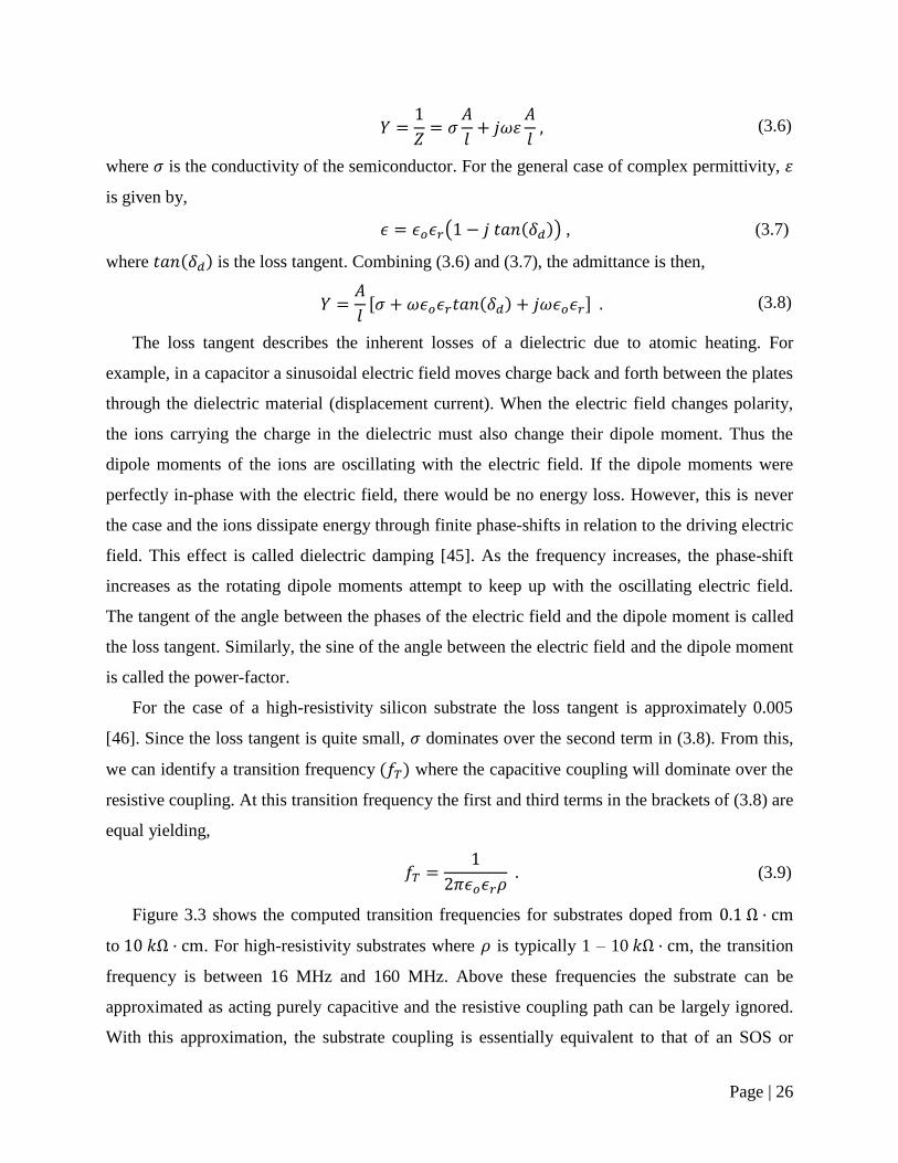
Figure 3.3 shows the computed transition frequencies for substrates doped from 0.1 Ω · cm
to 10 𝑘Ω · cm. For high-resistivity substrates where 𝜌 is typically 1 – 10 𝑘Ω · cm, the transition
frequency is between 16 MHz and 160 MHz. Above these frequencies the substrate can be
approximated as acting purely capacitive and the resistive coupling path can be largely ignored.
With this approximation, the substrate coupling is essentially equivalent to that of an SOS or

Page | 27
GaAs process [36]. Note that because the second term in (3.8) increases with frequency, at
sufficiently high frequencies, it can no longer be ignored. However, this should not occur until
around 30 GHz for a 1 𝑘Ω · cm substrate with 𝑡𝑎𝑛(𝛿𝑑) = 0.005. Hence, we can treat the high-
resistivity substrate as purely capacitive over a broad range of frequencies from approximately
100 MHz to 10 GHz.
3.1.1.1 Coplanar Strips
With the above conclusion that at sufficiently high frequencies the high-resistivity substrate
acts as an insulator, the high-frequency coupling behavior expected for the 100 µm long bars
from Figure 3.1 (and hence, for layouts of comparable structures on-chip) can be estimated using
capacitor formulas. If signals are coupled through the substrate only, the two bars can be
modeled as two coplanar strips (CPS) with a supporting dielectric below, as shown in Figure 3.4.
The capacitance per unit length between the CPS is given by (3.10) [47].
Figure 3.3 – Computed frequncies above which substrates behave more as a dielectric than a conductor.
Figure 3.4 – Cross-section of coplanar strips.
0.01
0.1
1
10
100
1000
10000
0.1 1 10 100 1000 10000
f T(G
Hz)
ρ (Ω·cm)

Page | 28
𝑐 = 휀0휀𝑒𝑓𝑓𝐾(𝑘0
′ )
𝐾(𝑘𝑜) (3.10)
where,
𝑘0 =
𝑠2
𝑤 +𝑠2
, 𝑘 =𝑠𝑖𝑛ℎ (
𝜋𝑠4ℎ)
𝑠𝑖𝑛ℎ (𝜋(𝑤 + 𝑔)
2ℎ) , 𝑘0
′ = √1 − 𝑘02 , 𝑘′ = √1 − 𝑘2
휀𝑒𝑓𝑓 = 1 + (휀 − 1)𝑞 , 𝑞 =1
2
𝐾(𝑘′)
𝐾(𝑘)
𝐾(𝑘0)
𝐾(𝑘0′ )
The function 𝐾() is the Complete Elliptic Integral of the First Kind given by,
𝐾(𝑘) = ∫𝑑𝜃
√1 − 𝑘2 𝑠𝑖𝑛2 𝜃
𝜋2
0
. (3.11)
If the substrate thickness ℎ is much larger than the spacing or width geometries of the CPS, then
as ℎ → ∞, 𝑘 → 𝑘0. Using this simplification in (3.10) yields,
𝑐 = 휀0 (1 +휀 − 1
2)𝐾(𝑘0
′ )
𝐾(𝑘0) . (3.12)
To eliminate the need to compute Elliptic Integrals, the following approximation can be made
[12]:
𝐾(𝑘0
′ )
𝐾(𝑘𝑜)≈
[
1
𝜋𝑙𝑛 (2
1 + √𝑘0′
1 − √𝑘0′)] for 0 ≤ 𝑘 ≤
1
√2
[1
𝜋𝑙𝑛 (2
1 + √𝑘0
1 − √𝑘0)]
−1
for 1
√2≤ 𝑘 ≤ 1
(3.13)
Equation (3.12) is defined for the case of a single layer of thick dielectric, which can be
assumed for signals injected into the high-resistivity thick-film SOI substrate (this situation will
be shown later if specific coupling mitigation strategies are used). For the cases of SOI where the
substrate resistance cannot be ignored, a more generalized formula for the capacitance of CPS
taking into account multiple layers of dielectrics is given in [48].

Page | 29
A family of capacitance per unit length plots for various spacing and width of CPS is shown
in Figure 3.5a. As expected, the capacitance falls off as the spacing between the bars increases.
This plot also shows a diminishing return on capacitance for increasing widths of the bars around
100 μm.
To help the reader understand the relationship between spacing and capacitance in CPS, these
parameters are compared to the familiar case of a parallel plate capacitor. The capacitance per
unit length of an equivalent parallel plate capacitor is given by,
𝑐 = 휀0휀𝑟𝑤
𝑠′ (3.14)
where 𝑠′ denotes the required separation of the plates to achieve the same capacitance from CPS
using (3.12) for a given space and width. The relationship between the separation of parallel
plates and CPS is shown in Figure 3.5b for different widths of CPS. Note that two 100 μm strips
separated by 20 μm have the same capacitance as two parallel plates which are 100 μm wide, but
separated by 70 μm. This is reasonable since the field lines for the CPS case are arcing from the
bottom of one strip to the bottom of the other and follow longer paths. Interestingly, for the
other extreme, where two 5 μm wide strips are separated by 100 μm, the capacitance is the same
as a parallel-plate configuration of two 5 μm wide strips separated by only about 7 μm. This is
consistent with the path widening up due to the divergence of the fields terminating on the strips.
Figure 3.5 – (a) Capacitance per unit length for CPS versus spacing and (b) equivalent spacing of a parallel
plate capacitor for the same capacitance as CPS.
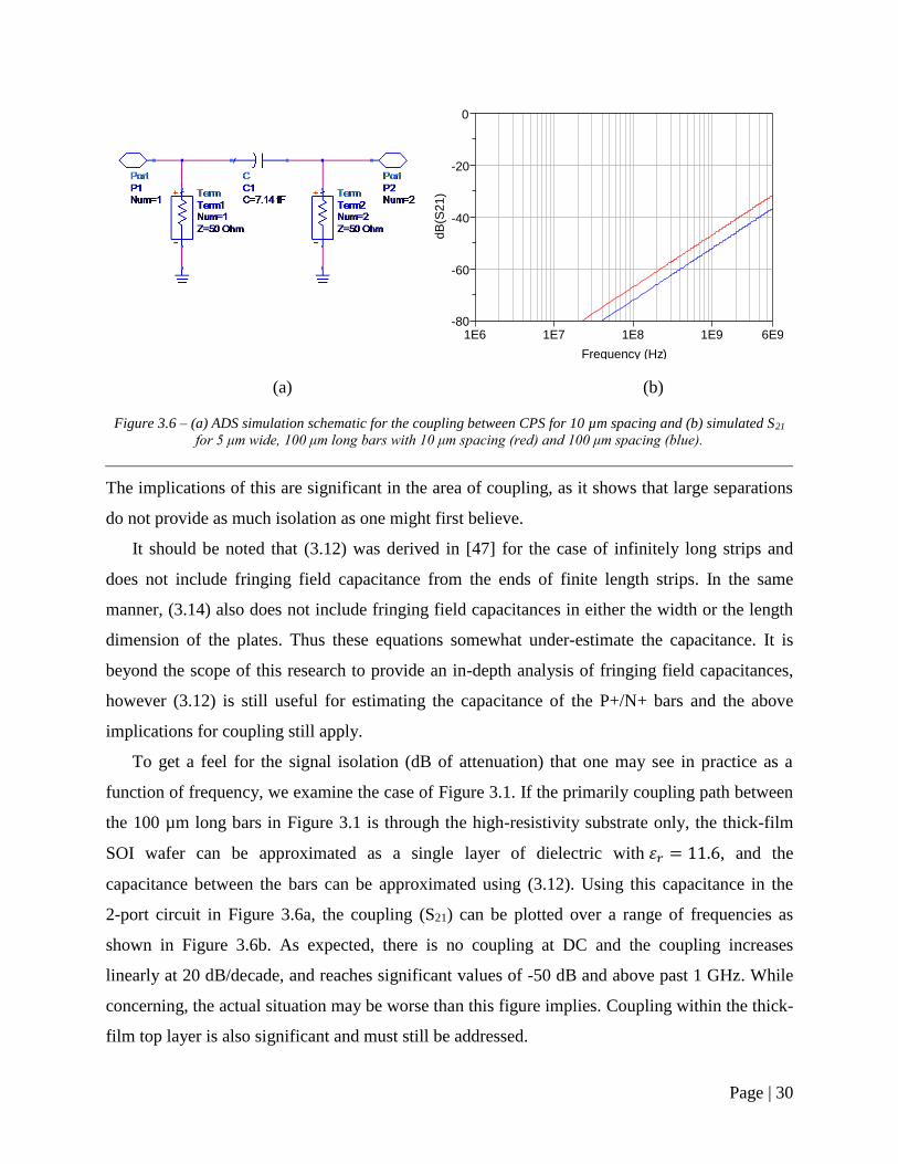
Page | 30
The implications of this are significant in the area of coupling, as it shows that large separations
do not provide as much isolation as one might first believe.
It should be noted that (3.12) was derived in [47] for the case of infinitely long strips and
does not include fringing field capacitance from the ends of finite length strips. In the same
manner, (3.14) also does not include fringing field capacitances in either the width or the length
dimension of the plates. Thus these equations somewhat under-estimate the capacitance. It is
beyond the scope of this research to provide an in-depth analysis of fringing field capacitances,
however (3.12) is still useful for estimating the capacitance of the P+/N+ bars and the above
implications for coupling still apply.
To get a feel for the signal isolation (dB of attenuation) that one may see in practice as a
function of frequency, we examine the case of Figure 3.1. If the primarily coupling path between
the 100 µm long bars in Figure 3.1 is through the high-resistivity substrate only, the thick-film
SOI wafer can be approximated as a single layer of dielectric with 휀𝑟 = 11.6, and the
capacitance between the bars can be approximated using (3.12). Using this capacitance in the
2-port circuit in Figure 3.6a, the coupling (S21) can be plotted over a range of frequencies as
shown in Figure 3.6b. As expected, there is no coupling at DC and the coupling increases
linearly at 20 dB/decade, and reaches significant values of -50 dB and above past 1 GHz. While
concerning, the actual situation may be worse than this figure implies. Coupling within the thick-
film top layer is also significant and must still be addressed.
(a) (b)
Figure 3.6 – (a) ADS simulation schematic for the coupling between CPS for 10 µm spacing and (b) simulated S21
for 5 μm wide, 100 μm long bars with 10 μm spacing (red) and 100 μm spacing (blue).
1E7 1E8 1E91E6 6E9
-60
-40
-20
-80
0
Frequency (Hz)
dB
(S21)

Page | 31
3.1.2 2D Surface Coupling through the Silicon Active-Layer
Coupling through the silicon active region at the surface in thick-film SOI is an important
contributor to crosstalk, just as it is in bulk-CMOS processes. MOSFETs built in properly biased
wells are diode-isolated due to the depletion regions setup around the active-device junctions.
The capacitance from the depletion regions prevent DC currents from flowing into the surface
[49]. However just as with the high-resistivity substrate, at sufficiently high frequencies
significant displacement currents can flow allowing signals to enter the active-layer where they
can couple to other parts of the circuit at great distances due to the low resistance of this layer.
In this section, the issue of active-layer coupling will be examined and combined with the
previous substrate coupling discussion using lumped element models. To simplify the surface
coupling analysis, the generator and receiver bars from Figure 3.1 considered first are P+
diffusion bars (as shown in Figure 3.7a). This allows the capacitive coupling mechanisms due to
diode-junctions to be addressed separately from the resistive coupling measurements. Later,
structures consisting of N+ diffusions containing depletion regions (Figure 3.7c) are investigated.
Figure 3.7 – (a) Diffusion generator and receiver P+ bars in p- active-layer and (b) the simplified lumped element
circuit coupling model. (c) N+ diffusion generator and receiver bars in p- active-layer and (d) the simplified lumped
element circuit coupling model.

Page | 32
These structures will show results more directly applicable to transistor source and drain
diffusions.
3.1.3 Lumped Element Coupling Models
One of the more intuitive ways to describe the coupling between the generator/receiver
structures is to look at the coupling impedances versus frequency for both the case of the P+ and
N+ diffusions bars in Figure 3.7. Designers can then take these models and scale them to
estimate coupling for their particular application. However, these models will not fully represent
the complex 2D and 3D fields and current paths that will actually be present in a chip. As noted
in [37], [43] and [50], simplified models such as the ones presented in Figure 3.7 still can
provide valuable insight into the issues of coupling in thick-film SOI.
In Figure 3.7a and Figure 3.7c, a signal generator will feed a signal into the generator P+ or
N+ diffused bar on the left. These bars make direct contact with the p- active-layer. In the case of
the P+ bar, the contact is ohmic and will not setup a depletion region. Currents will be resistivity
coupled into the active-layer and capacitively coupled into the high-resistivity substrate through
the BOX as previously elaborated. This type of contact could represent a P+ substrate contact
(PTAP) in an application circuit. For the other case, the N+ bar is a rectifying contact and will
setup a depletion region surrounding the bar. The capacitance from the depletion region will
prevent DC currents from entering the active-layer. Instead, AC currents can couple into the
active-layer, but otherwise the coupling paths are the same as for the P+ bar. The N+ contact
could represent the source or drain diffusion of a MOSFET.
To visually and numerically estimate the coupling between the generator/receiver bars in
Figure 3.7, simplified circuit models are shown in Figure 3.7b for the P+ bars and Figure 3.7d for
the N+ bars. In the models 𝑅𝑎𝑐𝑡𝑖𝑣𝑒, 𝐶𝐵𝑂𝑋 and 𝐶𝑠𝑢𝑏 represent respectively the resistive surface
coupling path through active-layer, the capacitance from vertical field lines passing from the
active-layer through the BOX to the substrate, and the capacitance from field lines through the
substrate that reach back to the other diffusion bar. The series capacitances 𝐶𝑓𝑖𝑙𝑙 between the
generator and receiver represent the capacitance from field lines that form a coupling path
through the metal-fill squares present above the circuit. In Figure 3.7d, 𝐶𝑑𝑒𝑝 represents the
depletion region capacitance resulting from the rectifying N+ contact. If the contact bars are
surrounded with deep-trench, a capacitance 𝐶𝐷𝑇 will be added to the models in series

Page | 33
with 𝑅𝑎𝑐𝑡𝑖𝑣𝑒. Also note that the DC coupling path 𝑅𝑠𝑢𝑏 is shown in the models, but grayed out.
As discussed previously, at frequencies above about 100 MHz this resistive coupling path can be
ignored.
3.1.3.1 Methods to Reduce Coupling
Due to the ohmic connections of the generator bar in the circuit model in Figure 3.7b, a
potentially strong DC-coupled path exists between the bars, while the rectifying nature of the
contacts in Figure 3.7d results an AC-coupled path with essentially the same resistive coupling at
sufficiently high frequencies. Potential methods of reducing the coupling can now be identified,
including:
increasing the value of 𝑅𝑎𝑐𝑡𝑖𝑣𝑒 by increasing the distance between the bars.
increasing the value of 𝑅𝑎𝑐𝑡𝑖𝑣𝑒 by blocking the channel-stopper implant,
introducing additional capacitance in series with 𝑅𝑎𝑐𝑡𝑖𝑣𝑒 by surrounding the bars with
deep-trench isolation walls (this will have a similar effect to 𝐶𝑑𝑒𝑝 in the N+ bar case
and will prevent DC currents from flowing into the active layer), and
removing 𝐶𝑓𝑖𝑙𝑙 by blocking the fill metals above the coupled bars.
Additionally, signals in the active-layer could potentially be shunted to ground through the use of
either PTAP or metal-only guard rings. Each of these potential coupling reducing methods is
examined in the sections to follow.
3.2 Experimental Array and Measurements
An experimental array consisting of 20 structures in the general form of Figure 3.1 using
different isolation strategies was fabricated in a commercial high-resistivity SOI process. In the
array there are 16 structures using the P+ generator/receiver form in Figure 3.7a and four
structures using the N+ form in Figure 3.7c. A photograph of the fabricated test array is shown in
Figure 3.8a.
In some of cells, the generator/receiver bar structures can clearly be seen. However, in others
the details of the cell are blocked by the metal-fill layers. A close up of one of the cells with the
metal-fill blocked is shown in Figure 3.8b. This cell consists of P+ diffusions bars separated by
10 μm with deep-trench isolations surrounding each bar. The fill-metals, represented by the
overlapping square pattern, are blocked in the region above the bars. In all of the cells the

Page | 34
channel-stopper implant is blocked in the region under the GSG probe pad structures to minimize
coupling to the pads as much as possible.
All of the structures were measured using an Agilent 8753E vector network analyzer with
150 μm pitch GSG probes. A full 2-port calibration was performed using a commercial
calibration substrate after allowing the VNA to warm up for four hours. The results below are
presented in a pair-wise fashion to best illustrate the effects of the different isolation techniques.
3.2.1 Blank Test Cell
Before the various coupling mitigation techniques can be compared, a baseline measurement
S21 floor must be established. The test cell in Figure 3.9a was fabricated without any P+ or N+
(a) (b)
Figure 3.8 – (a) Die photo of fabricated electric field coupling test-structure array. (b) Example
generator/receiver structure with deep-trench isolation surrounds and metal-fill layers blocked.
(a) (b)
Figure 3.9 – (a) Layout of blank test cell and (b) measured S21 of the blank test cell.
1E6 1E7 1E8 1E91E5 6E9
-60
-40
-20
-80
0
Frequency (Hz)
dB
(S21)
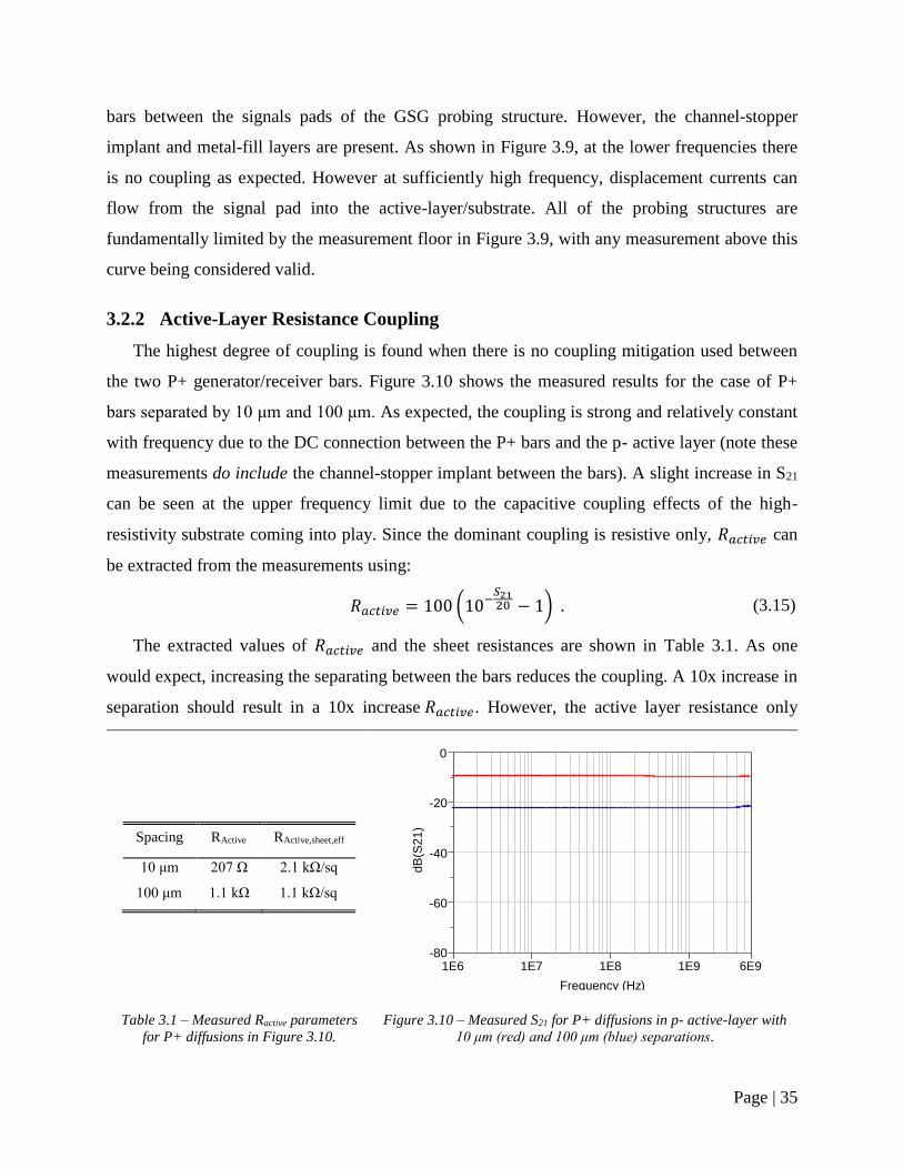
Page | 35
bars between the signals pads of the GSG probing structure. However, the channel-stopper
implant and metal-fill layers are present. As shown in Figure 3.9, at the lower frequencies there
is no coupling as expected. However at sufficiently high frequency, displacement currents can
flow from the signal pad into the active-layer/substrate. All of the probing structures are
fundamentally limited by the measurement floor in Figure 3.9, with any measurement above this
curve being considered valid.
3.2.2 Active-Layer Resistance Coupling
The highest degree of coupling is found when there is no coupling mitigation used between
the two P+ generator/receiver bars. Figure 3.10 shows the measured results for the case of P+
bars separated by 10 μm and 100 μm. As expected, the coupling is strong and relatively constant
with frequency due to the DC connection between the P+ bars and the p- active layer (note these
measurements do include the channel-stopper implant between the bars). A slight increase in S21
can be seen at the upper frequency limit due to the capacitive coupling effects of the high-
resistivity substrate coming into play. Since the dominant coupling is resistive only, 𝑅𝑎𝑐𝑡𝑖𝑣𝑒 can
be extracted from the measurements using:
𝑅𝑎𝑐𝑡𝑖𝑣𝑒 = 100 (10−𝑆2120 − 1) . (3.15)
The extracted values of 𝑅𝑎𝑐𝑡𝑖𝑣𝑒 and the sheet resistances are shown in Table 3.1. As one
would expect, increasing the separating between the bars reduces the coupling. A 10x increase in
separation should result in a 10x increase 𝑅𝑎𝑐𝑡𝑖𝑣𝑒. However, the active layer resistance only
Spacing RActive RActive,sheet,eff
10 μm 207 Ω 2.1 kΩ/sq
100 μm 1.1 kΩ 1.1 kΩ/sq
Table 3.1 – Measured Ractive parameters
for P+ diffusions in Figure 3.10.
Figure 3.10 – Measured S21 for P+ diffusions in p- active-layer with
10 μm (red) and 100 μm (blue) separations.
1E7 1E8 1E91E6 6E9
-60
-40
-20
-80
0
Frequency (Hz)
dB
(S21)
Page | 36
increased by about 5x. This discrepancy is believed to be due to fringing currents in the 100 μm
separation case coupling directly into the signal pad of the GSG probing structure.
3.2.3 Active-Layer Coupling with Channel-Stopper Implant Blocked
Coupling through the active-layer is a strong function of the doping level. Figure 3.11 shows
the coupling between P+ bars with the channel-stopper implant between the bars blocked for
10 μm and 100 μm bar separations. As shown in Table 3.2, blocking the channel-stopper implant
increases the active-layer sheet resistance by 100x relative to the previous case (recall the
channel-stopper is a shallow, high density P+ implant). Hence, one can expect a reduction in
coupling on the order of 40 dB if the channel-stopper implant is blocked. In Figure 3.11 this can
clearly be seen at the lower frequencies. Compared to the coupling in Figure 3.10, values below
50 MHz are improved by the expected 40 dB. However above 50 MHz, the coupling begins to
increase with frequency. This is expected as the reactance of the coupling path through the
substrate (𝑋𝑐) starts to dominate over the resistive coupling path through the active-layer at the
surface.
Table 3.2 – Measured Ractive and Xc parameters for the P+ diffusions with the channel-stopper implant blocked.
Spacing RActive RActive,Sheet Xc, f = 3 GHz Xc,Sheet,Eff, f = 3 GHz
10 μm 40 kΩ 400 kΩ/sq 2.4 kΩ 24 kΩ/sq
100 μm 125 kΩ 125 kΩ/sq 8.8 kΩ 8.8 kΩ/sq
Figure 3.11 – Measured S21 for P+ diffusions in p- active-layer with channel-stopper implant blocked with 10 μm
(red) and 100 μm (blue) separations.
1E7 1E8 1E91E6 6E9
-60
-40
-20
-80
0
Frequency (Hz)
dB
(S21)
Page | 37
At the lower frequencies, the resistance between the P+ bars can be computed using (3.15)
and is shown for both cases of 10 μm and 100 μm separations. Shown in the same table are the
approximate capacitive coupling reactances and effective sheet-reactance values at 3 GHz. The
reactance values are provided to give a baseline to compare the capacitive coupling in the other
test cases.
3.2.4 Coupling with Deep-Trench Isolation Surrounds
Coupling at frequencies below the high-resistivity substrate transition frequency can be
significantly reduced by adding capacitance in series with 𝑅𝑎𝑐𝑡𝑖𝑣𝑒 in the original circuit model
from Figure 3.7b. This series capacitance can be realized on-chip with deep-trench isolation
rings surrounding the generator and receiver bars. The circuit model in Figure 3.12 shows the
addition of series capacitance 𝐶𝐷𝑇 when employing deep-trench surrounds.
With the addition of the series capacitance, there should be no DC coupling path between the
bars. At high frequencies, displacement currents will begin to flow through the deep-trench
surrounds. Additionally at high frequencies, displacement currents will flow through the
substrate and the coupling will be similar to the previous case without the deep-trench surrounds
(assuming the channel-stopper is still blocked). Although 𝐶𝐷𝑇 is in series with 𝑅𝑎𝑐𝑡𝑖𝑣𝑒, it is not in
the same position as 𝐶𝐷𝑒𝑝 in the circuit model from Figure 3.7d. The capacitance from the
depletion region in the case of N+ bars completely surrounds the diffusions. Thus displacement
currents cannot flow into the active-layer or the high-resistivity substrate without first flowing
through the depletion region capacitance. However in the case of the P+ bars with deep-trench
surrounds, the capacitance does not completely enclose the P+ bar. Displacement currents can
Figure 3.12 – Simplified circuit model for P+ bars in p- active-layer with addition of deep-trench series
capacitance.

Page | 38
flow directly into the substrate, whereas signals entering the active-layer must flow through the
deep-trench capacitance.
The described behavior is clearly shown in Figure 3.13 when deep-trench surrounds are
added around the P+ bars. The net reactances and their corresponding sheet values are shown in
Table 3.3. Notice the effective sheet-reactances between the cases with and without deep-trench
surrounds are approximately the same (Table 3.2). Deep-trench only provides an increase in
isolation at lower frequencies, assuming that the channel-stopper implant is blocked between the
bars.
3.2.5 Deep-Trenches with Channel-Stopper Implant Present
If the channel-stopper implant is present in conjunction with deep-trenches surrounding the
P+ bars, increasing the distance between the two bars adds little improvement to the isolation, as
shown in Figure 3.14. As discussed previously, the deep-trenches create dielectric isolation on
the active-layer only. At sufficiently high frequencies, the reactances of the deep-trench walls are
low enough that displacement currents can flow and enter the active-layer. Due to the presence
of the channel-stopper implant, the impedance of the active-layer is relatively low (see 𝑅𝑎𝑐𝑡𝑖𝑣𝑒 in
Table 3.1) compared to impedance of the high-resistivity substrate (see 𝑋𝐶 in Table 3.3).
Spacing XDT
f = 3 GHz
Xc,Sheet,Eff
f = 3 GHz
10 μm 3.4 kΩ 34 kΩ/sq
100 μm 4.4 kΩ 4.4 kΩ/sq
Table 3.3 – Measured Xc values for the
P+ diffusions with deep-trench
surrounds extracted from Figure 3.13.
Figure 3.13 – Measured S21 for P+ diffusions in p- active-layer with
deep trench surrounds and channel-stopper implant blocked with 10 μm
(red) and 100 μm (blue) separations.
1E7 1E8 1E91E6 6E9
-60
-40
-20
-80
0
Frequency (Hz)dB
(S21)

Page | 39
3.2.6 Fill-Metal Coupling
The issue of coupling paths forming through metal-fill has been addressed in the past in [40]
and [41] where the effects of floating and grounded metal-fill of various geometries and patterns
were analyzed for different microwave interconnect topologies, such as microstrip, stripline and
CPW. Although fill can indeed affect these types topologies, where controlling the impedance of
the structure is important, the test structures in this thesis focus on metal-fill effects on coupling
paths over circuit blocks to determine if blocking fill is important in the coupling context.
3.2.6.1 Active-Layer Coupling with Fill-Metals Blocked
The coupling path created by the floating metal-fill shapes is shown in Figure 3.15a and in
the circuit models previously presented in Figure 3.7. The fill forms a chain of series
capacitances bridging the generator and receiver bars. The signal from the generator bar can
jump to the different layers of the floating metal-fill which act as the plates of capacitors with the
IMD acting as dielectric. Eventually the signal makes its way through the various metal-fill
layers until it reaches the receiver bar, forming an AC coupled path. However when this path is
prevented from forming by blocking the metal-fill between the bars, there is no significant
change in the coupling versus when metal-fill is present, as shown in Figure 3.15b (note bars do
not have deep-trench and the channel-stopper is present). This suggests that the coupling path
Figure 3.14 – Measured S21 for P+ diffusions in p- active-layer with deep trench surrounds with 10 μm (red) and
100 μm (blue) separations and channel-stopper present between the bars.
1E7 1E8 1E91E6 6E9
-60
-40
-20
-80
0
Frequency (Hz)
dB
(S21)

Page | 40
through the active-layer and substrate is lower than the path through the metal-fill, which follows
intuition when the sheet resistance values in Table 3.1 are reexamined.
To further illustrate fill has little effect on circuit block level coupling, deep-trench surrounds
can be added and the channel-stopper blocked between the P+ diffusion bars. The coupling for
such a configuration using 100 μm spaced bars is shown in Figure 3.16. With this configuration,
the effects of capacitance added by metal-fill should be prominent due to the higher isolation of
the bars. However, Figure 3.16 shows that the presence of the metal-fill only increases the
(a) (b)
Figure 3.15 – (a) Diagram showing coupling path formed from metal-fill. (b) Measured S21 for P+ diffusions in
p- active-layer with (red) and without (blue) metal-fill layers blocked with 100 μm separation.
Figure 3.16 – Measured S21 for P+ diffusions in p- active-layer with deep-trench surrounds and channel-stopper
blocked, with (red) and without (blue) the metal fill layers blocked, using 100 μm bar separation.
1E7 1E8 1E91E6 6E9
-60
-40
-20
-80
0
Frequency (Hz)
dB
(S21)
1E7 1E8 1E91E6 6E9
-60
-40
-20
-80
0
Frequency (Hz)
dB
(S21)

Page | 41
coupling by approximately 1 dB, and only at the high frequencies. This can be explained by
noting that the larger, higher-permittivity substrate presents a much lower impedance coupling
path than the chained capacitance of the metal-fill shapes.
3.2.6.2 Effects of Fill-Metal on Inter-Metal Coupling
Coupling between features on the same metal-layer could increase if the geometries of the fill
shapes is on the order of the metal features. Two test structures each consisting of 35
interdigitated Metal-1 fingers were fabricated and measured (Figure 3.18). Each finger is 5 μm
wide and 100 μm long with a spacing of 5 μm. These fingers act as a coplanar capacitor with the
IMD SiO2 as the dielectric. A simplified diagram of the structures is shown in Figure 3.17a. The
metal-fill layers were blocked above the fingers in Figure 3.18a and fill was added to the second
structure in Figure 3.18b on metal layers 2 through 6. In this figure the metal-fill can be clearly
seen and is approximately the same size as the spacing and width of the fingers. The Metal-6 fill
shapes are seen as gold colored squares and the Metal-5 fill shapes are seen as red colored
squares due to the optical distortion through the IMD SiO2. The fill shapes on metal layers 2
through 4 are obscured by the higher level fill. Both structures sit above a deep-trench grid,
allowing the effects of active-layer coupling to be minimized.
The lumped element coupling model is shown in Figure 3.17b. Similarly to the P+
generator/receiver bars in the previous section, the metal-fill creates a coupling path of chained
capacitances above the fingers. If this coupling path has a lower impedance than the coupling
path through the interdigitated fingers, then the capacitance, and therefore the coupling, of the
Figure 3.17 – (a) Simplified diagram of the Metal-1 interdigitated planar capacitor and (b) lumped element
circuit coupling model.

Page | 42
structure with fill should be higher than the structure without fill. As shown in Figure 3.19 this is
not the case. The difference in coupling between the two structures in only about 1 dB. Again we
can conclude that the effects of metal fill are essentially negligible when the whole picture
including substrate field-line coupling is considered.
Figure 3.18 – Photograph of the interdigitated Metal-1 structures, (a) with metal-fill and (b) without.
Figure 3.19 – Measured S21 of the interdigitated test structures in Figure 3.18 with (red) and without (blue)
metal-fill above the fingers.
1E7 1E8 1E91E6 6E9
-60
-40
-20
-80
0
Frequency (Hz)
dB
(S2
1)
Deep-trench Grid Metal-6 Fill Metal-5 Fill Metal-1 Fingers

Page | 43
3.2.7 Active-Layer Coupling with Metal-1 Guard-Rings
In PC board layouts, designers can form an electrostatic shield to reduce coupling by
surrounding noisy or sensitive circuits with a grounded metal ring. Parasitic electric field lines
reaching across the PC board will theoretically terminate at the low potential grounded guard-
ring. With this motivation, a test structure implementing an on-chip metal guard-ring was
fabricated and measured. Two P+ bars separated by 10 μm with the metal-fill and channel-
stopper implant blocked were surrounded by a 1 μm wide Metal-1 guard-ring as shown in Figure
3.20. Theoretically, a portion of the field lines through the surface of the active-layer should
terminate at the grounded guard-ring at sufficiently high frequencies. However, as shown in
Figure 3.20 – Diagram of P+ diffusions in p- active-layer with Metal-1 guard-ring.
Figure 3.21 – Measured S21 for P+ diffusions in p- active-layer with a metal-1 electrostatic guard-ring (red) and
without guard-ring (blue), with 10 μm separation (metal-fill and channel-stopper implant are blocked).
1E7 1E8 1E91E6 6E9
-60
-40
-20
-80
0
Frequency (Hz)
dB
(S21)
Page | 44
Figure 3.21 the addition of the Metal-1 guard rings shows little improvement over the test cell
without guard-rings.
Referring back to Figure 3.20, no direct DC path exists to the Metal-1 guard-ring from either
the generator or receiver bar. At sufficiently high frequency, displacement currents could flow
through the PMD dielectric and terminate at the grounded Metal-1 guard-ring. However, the
coupling path through the active-layer/substrate forms a lower impedance coupling path, largely
masking this effect.
3.2.8 N+ Diffusion Structures
In addition to the P+ bars in the p- active-layer, a series of N+ diffusion bars were also
fabricated. The N+ bars are NFETs with the gate, source and drain connected to the signal pad of
the GSG probing structure. By connecting the NFETs in this a manner, a zero-biased depletion
region capacitance around the N+ diffusions is created as shown in Figure 3.22 as dash lines. The
depletion regions around the N+ bars prevent DC currents from flowing into the active-layer,
similar to adding deep-trench surrounds in the P+ bar case. However unlike deep-trench
surrounds, the depletion region capacitances completely surround the N+ bars, including the
bottom surface, preventing currents from directly flowing to the active layer without first flowing
through the depletion region capacitance. Referring back to Figure 3.7d, the depletion region
capacitance 𝐶𝐷𝑒𝑝 appears in series with the coupling paths through the active-layer and substrate.
The similarities in coupling between P+ bars with deep-trench surrounds and the N+ bars
with depletion regions can clearly be seen in Figure 3.23a. Both offer very high isolation at low
Figure 3.22 – Diagram of the NFET test structure showing grounded body-ties on either side of the FETs.
Page | 45
frequencies and decreasing isolation as the frequency increases as capacitive coupling through
the substrate takes hold. Despite this similarity, Figure 3.23a reveals an interesting and important
difference between the two coupling mitigation strategies. Below approximately 1 GHz the slope
of S21 is 40 dB/decade for the NFET case, unlike the typical 20 dB/decade slope seen for the P+
bars with deep-trench surrounds. This 40 dB/decade slope yields slightly improved isolation at
the lower frequencies and degraded isolation at the high frequencies.
To explain this behavior, note the NFET devices actually have P+ diffusions (PTAPs) nearby
serving as active-layer body-ties, as shown in Figure 3.22. These P+ body-ties are grounded and
would be present in most application circuits. In this case they represent a body-tie near a FET
whose source is ungrounded, such as the case for differential amplifier designs. The body-ties
introduce a second zero into the 𝑆21 transfer function as can be seen from the lumped element
model in Figure 3.24. In this circuit model, one zero is formed by the CR high-pass filter formed
(a) (b)
Figure 3.23 – (a) Measured S21 for zero-biased NFETs with no coupling mitigation (red) and P+ diffusions in p-
active-layer with deep trench surrounds (blue), using two 100/0.18 μm NFETs with 10 μm separation. (b)
Simulated S21 for the former case.
Figure 3.24 – Lumped element model for Figure 3.22, with body-ties represented as resistors to ground.
1E7 1E8 1E91E6 6E9
-60
-40
-20
-80
0
Frequency (Hz)
dB
(S21)
1E7 1E8 1E91E6 6E9
-60
-40
-20
-80
0
Frequency (Hz)
dB
(S21)
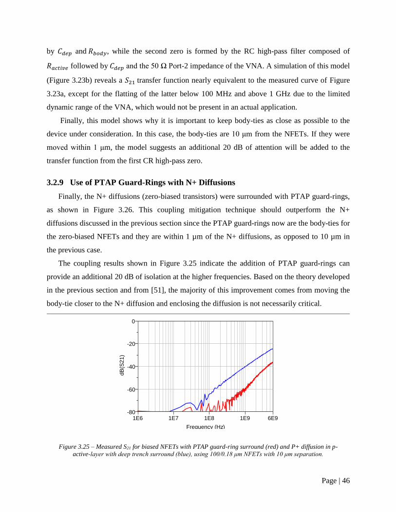
Page | 46
by 𝐶𝑑𝑒𝑝 and 𝑅𝑏𝑜𝑑𝑦, while the second zero is formed by the RC high-pass filter composed of
𝑅𝑎𝑐𝑡𝑖𝑣𝑒 followed by 𝐶𝑑𝑒𝑝 and the 50 Ω Port-2 impedance of the VNA. A simulation of this model
(Figure 3.23b) reveals a 𝑆21 transfer function nearly equivalent to the measured curve of Figure
3.23a, except for the flatting of the latter below 100 MHz and above 1 GHz due to the limited
dynamic range of the VNA, which would not be present in an actual application.
Finally, this model shows why it is important to keep body-ties as close as possible to the
device under consideration. In this case, the body-ties are 10 μm from the NFETs. If they were
moved within 1 μm, the model suggests an additional 20 dB of attention will be added to the
transfer function from the first CR high-pass zero.
3.2.9 Use of PTAP Guard-Rings with N+ Diffusions
Finally, the N+ diffusions (zero-biased transistors) were surrounded with PTAP guard-rings,
as shown in Figure 3.26. This coupling mitigation technique should outperform the N+
diffusions discussed in the previous section since the PTAP guard-rings now are the body-ties for
the zero-biased NFETs and they are within 1 µm of the N+ diffusions, as opposed to 10 µm in
the previous case.
The coupling results shown in Figure 3.25 indicate the addition of PTAP guard-rings can
provide an additional 20 dB of isolation at the higher frequencies. Based on the theory developed
in the previous section and from [51], the majority of this improvement comes from moving the
body-tie closer to the N+ diffusion and enclosing the diffusion is not necessarily critical.
Figure 3.25 – Measured S21 for biased NFETs with PTAP guard-ring surround (red) and P+ diffusion in p-
active-layer with deep trench surround (blue), using 100/0.18 μm NFETs with 10 μm separation.
1E7 1E8 1E91E6 6E9
-60
-40
-20
-80
0
Frequency (Hz)
dB
(S21)

Page | 47
3.3 Future Work
The third thick-film SOI coupling test chip designed is still being fabricated at the time of
this writing. This chip contains two additional test cells (shown in Figure 3.27) to characterize
electrical field coupling. The left-hand test cell contains an improved noise floor measurement
cell. This cell improves the original noise floor measurement cell from §3.2.1 by adding deep-
trench grids under the signal pads in the GSG probing structure. This reduces the capacitive
coupling from the signal pad to the active-layer. The channel-stopper implant is also blocked
between the two pads, increasing the sheet-resistance of the active-layer. Overall, this new noise
floor measurement cell will allow for better interpretation of test cells with very low coupling
such as the NFET cells, including the right-hand cell in Figure 3.27.
The right-hand test cell in Figure 3.27 consists of two N+ diffusion bars (zero-biased NFETs)
separated by 100 µm with the channel-stopper implant blocked between the bars. Each bar is
surrounded with a PTAP guard-ring then a deep-trench surround. Employing the most effective
isolation strategies investigated, this cell should have the highest degree of isolation.
Figure 3.26 – Diagram of N+ diffusions in p- active-layer with PTAP guard-ring surrounds.
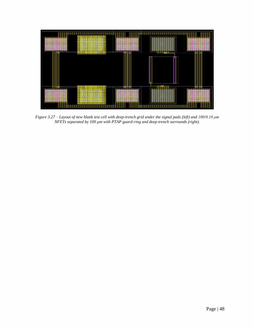
Page | 48
Figure 3.27 – Layout of new blank test cell with deep-trench grid under the signal pads (left) and 100/0.18 μm
NFETs separated by 100 µm with PTAP guard-ring and deep-trench surrounds (right).

Page | 49
4. Magnetic Coupling
Another potentially significant source of on-chip coupling is from magnetic fields. Circuits
flowing large currents can couple to nearby circuits via magnetic flux. In integrated radios such
as the KSU Micro-Transceiver, magnetic coupling can be particularly troublesome due to the
physically large and numerous inductors required to design circuits such as VCOs, LNAs, and
PAs. In particular, LNA inductors could pick up magnetic fields generated by the VDD and
ground traces in digital circuits, for instance when gate and flip-flop MOSFETs pull currents
when logic levels change state. As discussed previously, on the PC board-level magnetic
coupling can be reduced by employing ground planes to create image currents, and by enclosing
noisy circuit blocks in RF shields if radiated fields are of concern. A similar approach was taken
to reduce the magnetic coupling on-chip in the KSU Micro-Transceiver Radio research.
To quantify the degree to which the countermeasures adopted in that effort are effective, a
test structure was designed to investigate the reduction in magnetic coupling when a metal
“ground plane” was placed over a magnetically noisy digital circuit. The structure consists of a
circuit block designed to intentionally couple magnetically with a nearby on-chip spiral inductor,
as shown in Figure 4.1. The signals coupled into the receiver inductor from the circuit were
measured using a spectrum analyzer with and without the on-chip ground plane present.
4.1 Magnetic Coupling Analysis
Similar to the electric field coupling analysis, magnetic coupling on-chip can be analyzed
using the idea of generator and receiver structures. For this analysis, the generator/receiver
Figure 4.1 – Model of the basic magnetic test structure consisting of a noise generator and an on-chip planar
spiral inductor.
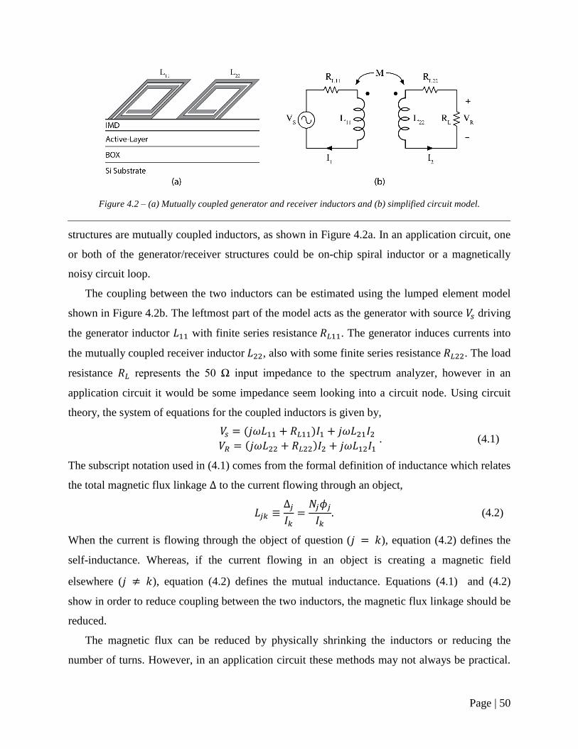
Page | 50
structures are mutually coupled inductors, as shown in Figure 4.2a. In an application circuit, one
or both of the generator/receiver structures could be on-chip spiral inductor or a magnetically
noisy circuit loop.
The coupling between the two inductors can be estimated using the lumped element model
shown in Figure 4.2b. The leftmost part of the model acts as the generator with source 𝑉𝑠 driving
the generator inductor 𝐿11 with finite series resistance 𝑅𝐿11. The generator induces currents into
the mutually coupled receiver inductor 𝐿22, also with some finite series resistance 𝑅𝐿22. The load
resistance 𝑅𝐿 represents the 50 Ω input impedance to the spectrum analyzer, however in an
application circuit it would be some impedance seem looking into a circuit node. Using circuit
theory, the system of equations for the coupled inductors is given by,
𝑉𝑠 = (𝑗𝜔𝐿11 + 𝑅𝐿11)𝐼1 + 𝑗𝜔𝐿21𝐼2𝑉𝑅 = (𝑗𝜔𝐿22 + 𝑅𝐿22)𝐼2 + 𝑗𝜔𝐿12𝐼1
. (4.1)
The subscript notation used in (4.1) comes from the formal definition of inductance which relates
the total magnetic flux linkage ∆ to the current flowing through an object,
𝐿𝑗𝑘 ≡∆𝑗
𝐼𝑘=𝑁𝑗𝜙𝑗
𝐼𝑘. (4.2)
When the current is flowing through the object of question (𝑗 = 𝑘), equation (4.2) defines the
self-inductance. Whereas, if the current flowing in an object is creating a magnetic field
elsewhere (𝑗 ≠ 𝑘), equation (4.2) defines the mutual inductance. Equations (4.1) and (4.2)
show in order to reduce coupling between the two inductors, the magnetic flux linkage should be
reduced.
The magnetic flux can be reduced by physically shrinking the inductors or reducing the
number of turns. However, in an application circuit these methods may not always be practical.
Figure 4.2 – (a) Mutually coupled generator and receiver inductors and (b) simplified circuit model.
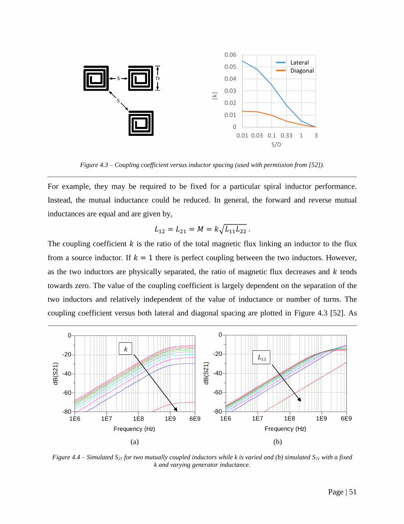
Page | 51
0
0.01
0.02
0.03
0.04
0.05
0.06
0.01 0.03 0.1 0.33 1 3
|k|
S/D
For example, they may be required to be fixed for a particular spiral inductor performance.
Instead, the mutual inductance could be reduced. In general, the forward and reverse mutual
inductances are equal and are given by,
𝐿12 = 𝐿21 = 𝑀 = 𝑘√𝐿11𝐿22 .
The coupling coefficient 𝑘 is the ratio of the total magnetic flux linking an inductor to the flux
from a source inductor. If 𝑘 = 1 there is perfect coupling between the two inductors. However,
as the two inductors are physically separated, the ratio of magnetic flux decreases and 𝑘 tends
towards zero. The value of the coupling coefficient is largely dependent on the separation of the
two inductors and relatively independent of the value of inductance or number of turns. The
coupling coefficient versus both lateral and diagonal spacing are plotted in Figure 4.3 [52]. As
Figure 4.3 – Coupling coefficient versus inductor spacing (used with permission from [52]).
(a) (b)
Figure 4.4 – Simulated S21 for two mutually coupled inductors while k is varied and (b) simulated S21 with a fixed
k and varying generator inductance.
1E7 1E8 1E91E6 6E9
-60
-40
-20
-80
0
Frequency (Hz)
dB
(S2
1)
1E7 1E8 1E91E6 6E9
-60
-40
-20
-80
0
Frequency (Hz)
dB
(S2
1)
Lateral Diagonal
𝑘
𝐿11
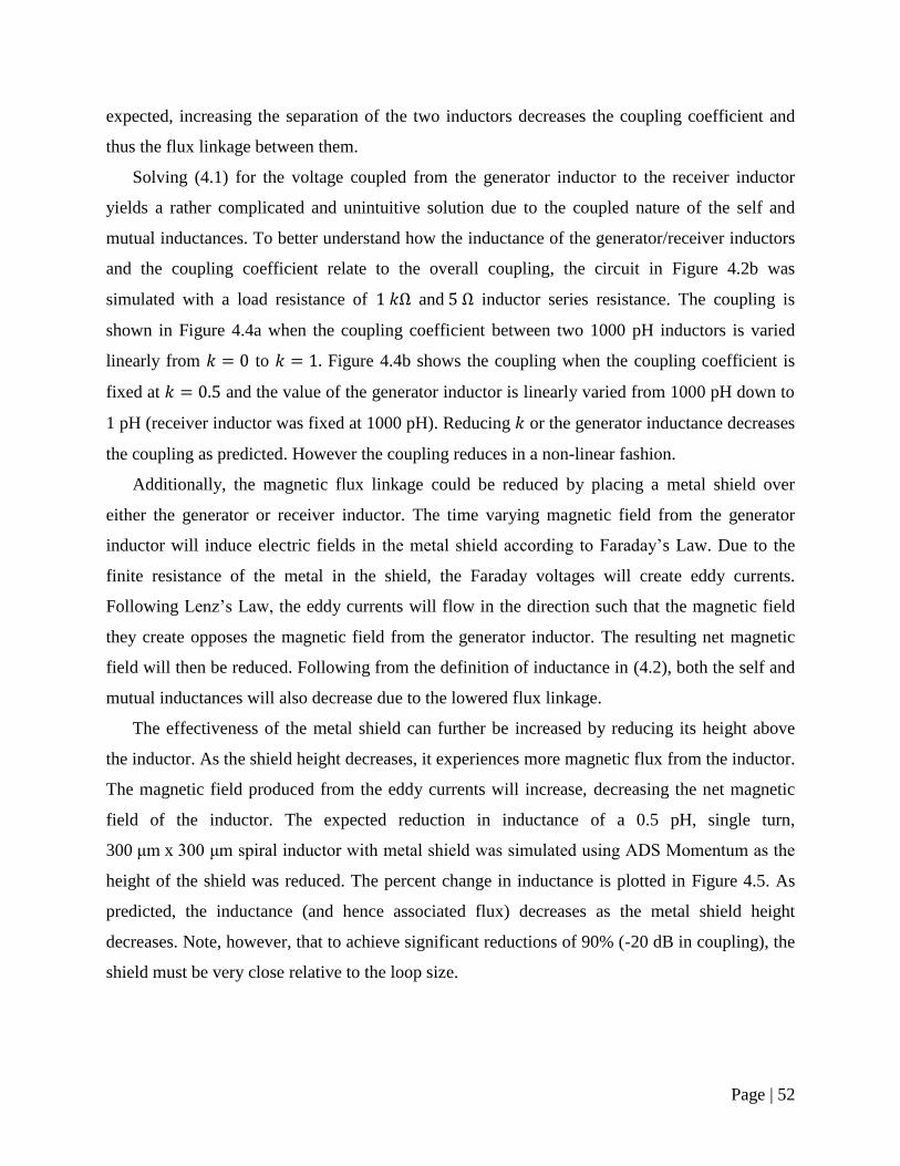
Page | 52
expected, increasing the separation of the two inductors decreases the coupling coefficient and
thus the flux linkage between them.
Solving (4.1) for the voltage coupled from the generator inductor to the receiver inductor
yields a rather complicated and unintuitive solution due to the coupled nature of the self and
mutual inductances. To better understand how the inductance of the generator/receiver inductors
and the coupling coefficient relate to the overall coupling, the circuit in Figure 4.2b was
simulated with a load resistance of 1 𝑘Ω and 5 Ω inductor series resistance. The coupling is
shown in Figure 4.4a when the coupling coefficient between two 1000 pH inductors is varied
linearly from 𝑘 = 0 to 𝑘 = 1. Figure 4.4b shows the coupling when the coupling coefficient is
fixed at 𝑘 = 0.5 and the value of the generator inductor is linearly varied from 1000 pH down to
1 pH (receiver inductor was fixed at 1000 pH). Reducing 𝑘 or the generator inductance decreases
the coupling as predicted. However the coupling reduces in a non-linear fashion.
Additionally, the magnetic flux linkage could be reduced by placing a metal shield over
either the generator or receiver inductor. The time varying magnetic field from the generator
inductor will induce electric fields in the metal shield according to Faraday’s Law. Due to the
finite resistance of the metal in the shield, the Faraday voltages will create eddy currents.
Following Lenz’s Law, the eddy currents will flow in the direction such that the magnetic field
they create opposes the magnetic field from the generator inductor. The resulting net magnetic
field will then be reduced. Following from the definition of inductance in (4.2), both the self and
mutual inductances will also decrease due to the lowered flux linkage.
The effectiveness of the metal shield can further be increased by reducing its height above
the inductor. As the shield height decreases, it experiences more magnetic flux from the inductor.
The magnetic field produced from the eddy currents will increase, decreasing the net magnetic
field of the inductor. The expected reduction in inductance of a 0.5 pH, single turn,
300 μm x 300 μm spiral inductor with metal shield was simulated using ADS Momentum as the
height of the shield was reduced. The percent change in inductance is plotted in Figure 4.5. As
predicted, the inductance (and hence associated flux) decreases as the metal shield height
decreases. Note, however, that to achieve significant reductions of 90% (-20 dB in coupling), the
shield must be very close relative to the loop size.
Page | 53
Designers of RF circuits should be aware that placing a metal shield over an inductor will
decrease its quality-factor in addition to its inductance. The quality-factor of any resonate system
is defined as,
𝑄 ≡ 2𝜋𝐸𝑛𝑒𝑟𝑔𝑦 𝑠𝑡𝑜𝑟𝑒𝑑
𝐸𝑛𝑒𝑟𝑔𝑦 𝑑𝑖𝑠𝑠𝑖𝑝𝑎𝑡𝑒𝑑 𝑝𝑒𝑟 𝑐𝑦𝑐𝑙𝑒 . (4.3)
Due to the finite resistance of the metal shield, the induced eddy currents dissipate energy and
from (4.3) reduces the Q of the inductor. Designers should avoid using metal shields over
circuits requiring high-Q inductors, such as LNAs, VCOs, and PAs. The preceding analysis is
primarily useful for decreasing the flux generated by a digital circuit, where a ground plane is
placed over the digital circuits to help reduce their magnetic fields. To characterize how much
reduction may be achieved in practice, a set of test structures was developed and measured.
4.2 Experimental Structure and Measurements
The magnetic coupling experimental test structure shown in Figure 4.6a was fabricated in an
SOI process with a high-resistivity silicon substrate (reducing any confounding effects from eddy
currents in the substrate). The structure consists of a planar spiral receiver inductor and two
digital circuit magnetic noise generators. However much of the detail is obfuscated by the metal-
fill, therefore Figure 4.6b is provided showing the layout of the structure before the metal-fill
Figure 4.5 – Plot of the reduction of inductance in a single loop inductor due to metal shield height.
0
10
20
30
40
50
60
70
80
90
100
1 10 100
Per
cen
t R
edu
ctio
n o
f In
du
ctan
ce (
%)
Shield Height Above Inductor (µm)

Page | 54
layers were added. The right-most and top-most generator structures are identical in form, except
the top-most structure employs a metal magnetic shield (the bottom structure is not used in this
experiment). An HP8592L spectrum analyzer with 150 µm pitch GSG RF probes was used to
measure the signals coupled from the two structures into the receiver inductor.
An enlarged view of the generator structures is shown in Figure 4.7. Each consists of a
3 GHz CMOS ring oscillator with buffered output. The output buffer is a 7-stage CMOS
exponential horn with a 2x scale factor. A bypass capacitor and VDD/ground pads are also
provided. Each of the generator structures is individually powered using 50 Ω ground-signal
“ant-head” probes landed on 60 µm x 60 µm probe pads supplied with 1.8 VDC
The generators are intentionally designed to generate magnetic flux and to magnetically
couple with the receiver inductor. On each rising and falling edge of the oscillator clock, the
inverters of the buffer will switch state and pull a near impulse-like current from the power
Figure 4.6 – (a) Photograph of fabricated magnetic test structure and (b) layout view of the structure.
Figure 4.7 – Layout of a generator structure from Figure 4.6.
Shielded
Unshielded
VDD GND
Bypass
Capacitor
Buffer Ring
Oscillator

Page | 55
supply bypass capacitor (see Figure 4.8a). As the inverters of the buffer increase in size, the
current they pull from the capacitor also increases. The inverters are connected to the power
supply rails using a bus-topology, thus subsequent inverters are physically farther from the
source and create a larger current loop from the VDD and ground traces (Figure 4.8b). The
currents in the loop create a magnetic field around the supply traces according to Ampère's Law
(indicated with the crossed circles in Figure 4.8b). The magnetic flux from the generator
structures will couple into the receiver inductor and induce a voltage that can be measured with
the spectrum analyzer. The shielded generator structure has a Metal-6 shield connected to ground
covering the ring oscillator, buffer and the VDD/ground traces.
Note that in Figure 4.7 and the schematic in Figure 4.8b, the bypass capacitor is placed near
the lower current ring oscillator, and farthest from the highest-current inverter. In a typical well-
designed application circuit, most of the switching transients from the generator structures could
be reduced by placing an adequately sized bypass capacitor close to the highest current part of
the circuit. However, to ensure a sufficiently sized magnetic loop is formed for this test circuit,
the bypass capacitor was placed on the low current side of the structure near the ring oscillator.
The generator structures are positioned 50 µm away from the receiver inductor. The receiver
inductor is a 300 µm x 300 µm planar spiral inductor with 5 turns. To reduce the amount of
electric field coupling from the noise generators to the receiver inductor, a deep-trench grid was
placed under the inductor and the GSG probing structure. The position of the two generator
structures around the receiver inductor will lead to slightly different coupling coefficients. The
Figure 4.8 – (a) CMOS inverter switching characteristics and (b) schematic of the basic generator structure
showing currents and magnetic field lines.
Page | 56
shielded structure (top-most structure in Figure 4.6) is closer to the GSG probing structure and
parallel to the crossover of the inductor which is in turn connected to the signal pad of the GSG
structure. This increases the coupling coefficient between the shielded structure and the receiver
inductor, making the performance of the shielded structure appear worse than it would in
practice.
The signals coupled from unshielded and shielded generator structures into the receiver
inductor were measured separately using a spectrum analyzer. The data was captured from the
instrument using the custom LabVIEW program detailed in Appendix A and plotted in Figure
4.9. The rise in the noise floor around 6.5 GHz and 13 GHz is due to the multi-banded nature of
the HP8592L spectrum analyzer used. To ensure both the noise generators were producing the
same currents, the current consumption during measurement was verified to be approximately
13 mA (±5%). The coupled frequency of the unshielded generator and its harmonics are shown
out to 18 GHz in the top plot in Figure 4.9. The signal coupled from the shielded generator is
shown in the bottom plot.
Placing a metal shield over the generator structure reduced the magnetic coupling by
approximately 10 dB. As seen over the wide frequency range of the harmonics from the
generators, the effectiveness of the metal shield remained nearly constant over frequency. This is
expected because Faraday induction and production of eddy currents is independent of frequency
in linear materials. The effectiveness of the shield could be increased, however, by reducing its
height above the generator structure. The metal shield as designed in Figure 4.6 is located on
Metal-6, approximately 5 μm above the active-layer. Decreasing the height of the shield by
moving it to a lower metal layer, such as Metal-2 or Metal-3, could reduce the loop inductance of
the generator by 10 – 15% according to Figure 4.5 and thereby further decrease the coupling.

Page | 57
Figure 4.9 – Magnetic coupling without metal shield (top) and with metal shield (bottom).
-100
-90
-80
-70
-60
-50
-40
1 3 5 7 9 11 13 15 17
Po
wer
(d
Bm
)
Frequency (GHz)
Unshielded Couping
-100
-90
-80
-70
-60
-50
-40
1 3 5 7 9 11 13 15 17
Po
wer
(d
Bm
)
Frequency (GHz)
Shielded Coupling

Page | 58
4.3 Future Work
To better characterize the effectiveness of the metal shield at lower frequencies, a revised
magnetic structure was designed, as shown in Figure 4.10. This structure operates in the same
manner as before, except the generators use a variable oscillator instead of a fixed frequency ring
oscillator, allowing the frequency of the generators to be tuned from 0 – 2 GHz. At the time of
writing, the IC with this structure was still in manufacturing and measurements are not included
in this thesis.
The variable oscillator is a current-starved VCO (CS-VCO) [53]. The schematic is shown in
Figure 4.11 and the layout is shown in Figure 4.12. At its core, the CS-VCO is a ring oscillator
composed of inverters (M4 and M5). However, the current flowing through the inverters of the
ring oscillator can be controlled using M3 and M6. By restricting the current flow through the
inverters, the oscillation frequency will decrease according to:
𝑓𝑜𝑠𝑐 =𝐼𝐷
𝐶𝑡𝑜𝑡𝑉𝐷𝐷𝑁 . (4.4)
The output of the CS-VCO is buffered using an exponential horn with a 3x scale-factor. The
scale-factor was increased from the previous design to increase the relative current drawn from
the power supply in the last inverter, thus increasing the magnetic field created in the generator
structures and coupling more energy into the receiver inductor, increasing the SNR.
In addition to the VDD and GND pads, a separate set of pads are provided in Figure 4.10 for
the tuning voltage and ground. The tune signal is connected directly to the gate of a MOSFET.
Therefore ESD diodes and clamping circuitry are provided to prevent damage from ESD.

Page | 59
Figure 4.10 – Magnetic test structure with variable frequency noise generators.
Shielded
Unshielded
VDD
VDD
GND
GND
GND
GND Vtune
Vtune
Clamp
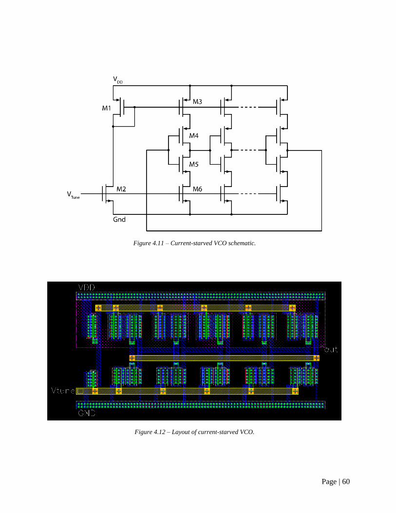
Page | 60
Figure 4.11 – Current-starved VCO schematic.
Figure 4.12 – Layout of current-starved VCO.

Page | 61
5. Bond Pad Coupling
As chips become denser and more integrated, the size, density, and separation of bond pads
must also decrease. Mixed-signal designs, such as the KSU Micro-Transceiver Radio, need to
interface strong digital and weak analog signals from the host circuit board to the chip. Due to
system architecture and layout requirements, these signals may be on physically close bond pads.
This situation has the potential for strong-signal digital bonds pads to act as generators and inject
signals into the active-layer and substrate of the chip. These signals could couple onto nearby
bond pads, degrading system performance.
High isolation RF pads have been studied in the past in bulk-CMOS processes [54], [55].
However, comparatively little literature exists for bond pad coupling in SOI processes. In this
chapter, the coupling mitigation theory and techniques developed in the previous chapters will be
applied to analyze the coupling between bond pads.
Unlike the P+/N+ bars, the bond pads do not make contact to the active-layer. The pads are
separated from the active-layer by the PMD and IMD insulators, therefore no DC coupling path
exists. However, at sufficiently high frequencies, displacement currents can flow through the
insulators and into the active-layer and substrate. In this research, no active devices are present
under the pads. However due to the increasing density of ICs, common practice is to place ESD
protection circuitry directly under the bond pads [56]. Due to the lack of active devices under the
bond pads used in this thesis, the active-layer regions directly under the pads will be doped by
default with channel-stopped implant, potentially causing a high degree of coupling.
The displacement currents coupled into the active-layer could be reduced by blocking the
channel-stopper implant or by increasing the separation of the pads. In lower density designs
where high numbers of bond pads are not required, a grounded pad could also be inserted
between the generator and receiver pads of a coupling-sensitive design, increasing their
separation. The added bond pad could be bonded to an off-chip ground, helping to create an
electric field shielding function and further reducing ground-bounces issues.
Furthermore, adding a deep-trench grid under the pad could significantly increase the
impedance of the active-layer. Finally, in a similar fashion to using buried layers in bulk-CMOS
technologies, an equipotential surface could also be placed under the pad such as a metal ground
shield on a lower layer, or by grounding the active-layer through the use of PTAP guard-rings.

Page | 62
5.1 Experimental Array and Measurements
A cross-sectional view of a nominal Metal-6 pad with no coupling mitigation techniques is
shown in Figure 5.2a. Three different coupling mitigation techniques applied to the nominal pad
include:
placing a deep-trench grid under the pad (Figure 5.2b),
placing a PTAP guard-ring around the perimeter of the pad (Figure 5.2c) and
inserting a grounded Metal-1 shield under the pad with deep-trench (Figure 5.2d).
Note that the geometries in Figure 5.2 are exaggerated to show the details of the coupling
mitigation strategies used. In reality, the dimensions of the pads are about two orders of
magnitude greater than their distance from the surface of the active-layer.
Eight bond-pad coupling structures were designed and fabricated. A photograph of the
fabricated die is shown in Figure 5.1. The pads are 100 μm x 100 μm Metal-6 pads and do not
contain any ESD protection diodes or clamping circuitry. Four of the structures consist of the 3-
pad variant shown in Figure 5.3a and the remaining four structures consist of the 4-pad variant
shown in Figure 5.3b. Each has an associated digital oscillator that drives the digital pad and is
powered by a separate pair of probing pads.
The 3-pad variant consists of a generator pad (tied to the on-chip digital oscillator), a receiver
pad and a ground pad. A 150 µm pitch Signal-Ground (SG) RF probe was landed on the receiver
and ground pads to measure the coupling from
the generator pad to the receiver pad. The 4-pad
variant inserts an addition ground pad between
the generator and receiver pads. The additional
pad is grounded to the same domain as the
generator pad in an attempt to capture part of the
generated electric field flux. The bottom ground
pad in this variant is again used as the ground for
the SG probe. The coupling structures in the 3-
pad and 4-pad variants each contain one of the
coupling mitigation techniques from Figure 5.2.
In each structure, the coupling mitigation
technique is applied to all pads.
Figure 5.1 – Photograph of the pad coupling test
structure chip.

Page | 63
Figure 5.2 –Diagram of the different bond pad coupling mitigation techniques.
Figure 5.3 – Bond pad coupling test structures showing the (a) 3-pad and (b) 4-pad variant structures.
Buffered Ring
Oscillator

Page | 64
In both the 3-pad and 4-pad variants, the generator pad is driven by a 1.5 GHz ring oscillator
and buffer similar to the ones used in the magnetic coupling test structures in §4.2. However, the
buffered ring oscillators are properly decoupled (bypass capacitor placed near the high current
devices), surrounded by a deep-trench grid and located 200 μm away from the bond pads. These
electric field coupling mitigation strategies reduce currents coupled into the active-layer and
substrate from the buffered ring oscillators below the measurement noise floor. Finally, the
buffered ring oscillators are powered from 1.8 VDC using “ant-head” probes.
The strength of the 1.5 GHz fundamental of the ring oscillator coupled from the generator
pad to the receiver pad was measured using an HP ESA-L1500A spectrum analyzer for each of
the eight pad coupling structures and the relative measured signal levels were compared. To
ensure that the generator pads in each of the eight structures were producing the same strength
signal, the current from the buffered ring oscillators was monitored. The nominal current draw
was 6.8 mA (±9.3%) and the ring oscillator fundamental frequency varied by 3.7%. The slight
variation in fundamental frequency and current is small enough that it will not affect the signal
power coupled from the generator pad to the receiver pad. The measured coupling from the
Figure 5.4 – Measured strength of the fundamental of the signal (1.5 GHz) coupled from the generator pad to the
receiver pad for both the 3-pad (left) and 4-pad test structures (right).
-60.00
-50.00
-40.00
-30.00
-20.00
-10.00
0.00
M6 PadOnly DT Grid
PTAP GuardRing
M1 GNDShield + DT
M6 PadOnly DT Grid
PTAP GuardRing
M1 GNDShield + DT
3-Pad Variant 4-Pad Variant
Sign
al S
tren
gth
on
Rec
eive
r P
ad (
dB
m)
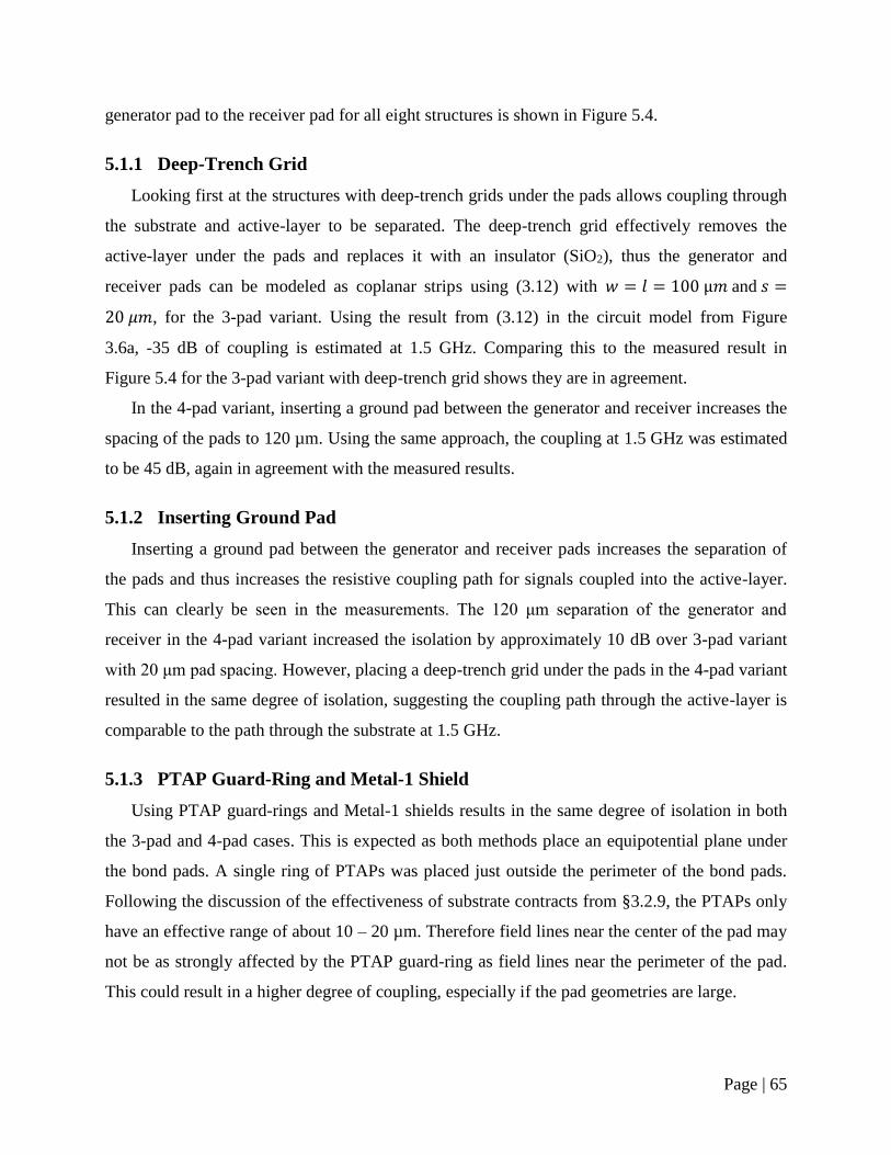
Page | 65
generator pad to the receiver pad for all eight structures is shown in Figure 5.4.
5.1.1 Deep-Trench Grid
Looking first at the structures with deep-trench grids under the pads allows coupling through
the substrate and active-layer to be separated. The deep-trench grid effectively removes the
active-layer under the pads and replaces it with an insulator (SiO2), thus the generator and
receiver pads can be modeled as coplanar strips using (3.12) with 𝑤 = 𝑙 = 100 µ𝑚 and 𝑠 =
20 𝜇𝑚, for the 3-pad variant. Using the result from (3.12) in the circuit model from Figure
3.6a, -35 dB of coupling is estimated at 1.5 GHz. Comparing this to the measured result in
Figure 5.4 for the 3-pad variant with deep-trench grid shows they are in agreement.
In the 4-pad variant, inserting a ground pad between the generator and receiver increases the
spacing of the pads to 120 µm. Using the same approach, the coupling at 1.5 GHz was estimated
to be 45 dB, again in agreement with the measured results.
5.1.2 Inserting Ground Pad
Inserting a ground pad between the generator and receiver pads increases the separation of
the pads and thus increases the resistive coupling path for signals coupled into the active-layer.
This can clearly be seen in the measurements. The 120 μm separation of the generator and
receiver in the 4-pad variant increased the isolation by approximately 10 dB over 3-pad variant
with 20 μm pad spacing. However, placing a deep-trench grid under the pads in the 4-pad variant
resulted in the same degree of isolation, suggesting the coupling path through the active-layer is
comparable to the path through the substrate at 1.5 GHz.
5.1.3 PTAP Guard-Ring and Metal-1 Shield
Using PTAP guard-rings and Metal-1 shields results in the same degree of isolation in both
the 3-pad and 4-pad cases. This is expected as both methods place an equipotential plane under
the bond pads. A single ring of PTAPs was placed just outside the perimeter of the bond pads.
Following the discussion of the effectiveness of substrate contracts from §3.2.9, the PTAPs only
have an effective range of about 10 – 20 µm. Therefore field lines near the center of the pad may
not be as strongly affected by the PTAP guard-ring as field lines near the perimeter of the pad.
This could result in a higher degree of coupling, especially if the pad geometries are large.
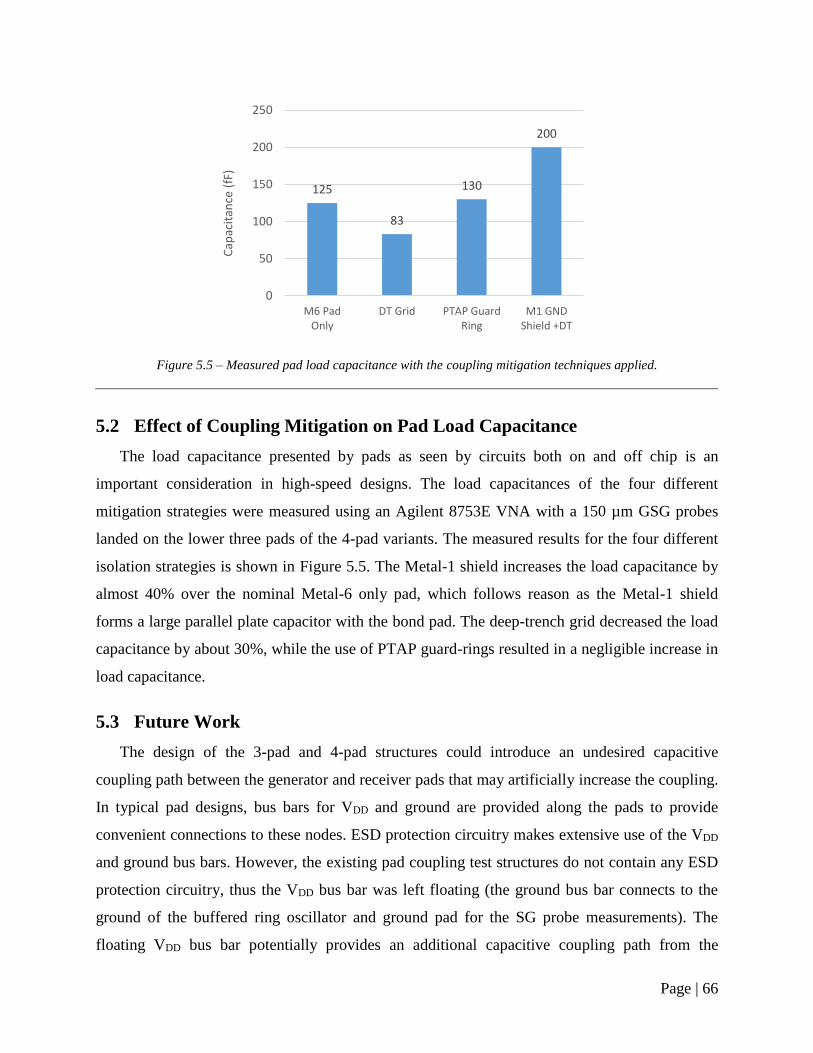
Page | 66
5.2 Effect of Coupling Mitigation on Pad Load Capacitance
The load capacitance presented by pads as seen by circuits both on and off chip is an
important consideration in high-speed designs. The load capacitances of the four different
mitigation strategies were measured using an Agilent 8753E VNA with a 150 µm GSG probes
landed on the lower three pads of the 4-pad variants. The measured results for the four different
isolation strategies is shown in Figure 5.5. The Metal-1 shield increases the load capacitance by
almost 40% over the nominal Metal-6 only pad, which follows reason as the Metal-1 shield
forms a large parallel plate capacitor with the bond pad. The deep-trench grid decreased the load
capacitance by about 30%, while the use of PTAP guard-rings resulted in a negligible increase in
load capacitance.
5.3 Future Work
The design of the 3-pad and 4-pad structures could introduce an undesired capacitive
coupling path between the generator and receiver pads that may artificially increase the coupling.
In typical pad designs, bus bars for VDD and ground are provided along the pads to provide
convenient connections to these nodes. ESD protection circuitry makes extensive use of the VDD
and ground bus bars. However, the existing pad coupling test structures do not contain any ESD
protection circuitry, thus the VDD bus bar was left floating (the ground bus bar connects to the
ground of the buffered ring oscillator and ground pad for the SG probe measurements). The
floating VDD bus bar potentially provides an additional capacitive coupling path from the
Figure 5.5 – Measured pad load capacitance with the coupling mitigation techniques applied.
125
83
130
200
0
50
100
150
200
250
M6 PadOnly
DT Grid PTAP GuardRing
M1 GNDShield +DT
Cap
acit
ance
(fF
)

Page | 67
generator pad to the receiver pad, as shown in Figure 5.6. Signals could couple from the
generator pad flyover on to the floating VDD bus bar, and then couple to the receiver pad through
its flyover.
A new series of pad coupling test structures was designed removing the floating VDD bus
bars. The chip (shown in Figure 5.7) was still in manufacturing at the time of writing. This chip
contains pads using the coupling mitigation techniques discussed previously. An additional
structure containing ESD protection circuitry is provided to characterize the effect of ESD diodes
and ESD clamps on the pad coupling. Finally, a structure containing a floating VDD bar is
provided to compare coupling results to the structures with the floating VDD bar removed.
Figure 5.6 – Diagram showing coupling path between bond pads through a floating VDD bus bar.
VDD Bus Bar
(Floating)
50 Ω
Fly-Over
GND Bus Bar
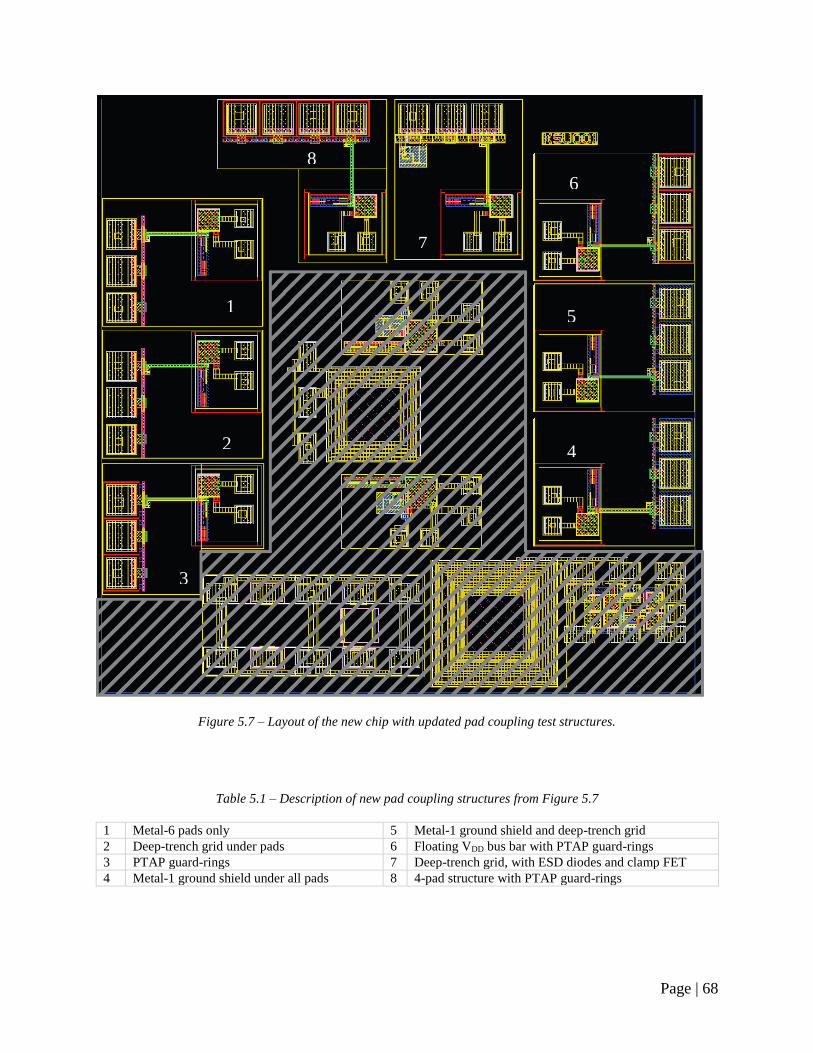
Page | 68
Figure 5.7 – Layout of the new chip with updated pad coupling test structures.
Table 5.1 – Description of new pad coupling structures from Figure 5.7
1 Metal-6 pads only 5 Metal-1 ground shield and deep-trench grid
2 Deep-trench grid under pads 6 Floating VDD bus bar with PTAP guard-rings
3 PTAP guard-rings 7 Deep-trench grid, with ESD diodes and clamp FET
4 Metal-1 ground shield under all pads 8 4-pad structure with PTAP guard-rings
1
2
3
4
5
6
7
8
Page | 69
6. Conclusion
This research examined coupling mechanisms in high-resistivity thick-film SOI. Both
electric and magnetic field coupling mechanisms were analyzed using the concept of generator
and receiver structures. For both cases, lumped element coupling models were developed to
assist the coupling analysis. Utilizing mitigation techniques developed in the electric field
analysis, coupling between bond pads was also assessed.
6.1 Electric Field Coupling
In thick-film SOI when no coupling mitigation techniques were employed, electric field
coupling was significant and relativity constant with frequency. Simply blocking the channel-
stopper implant reduced coupling at the lower frequencies by over 40 dB, with coupling at lower
frequencies further reduced with the addition of deep-trench surrounds. The depletion region
created by zero- or reversed-biased MOSFETs also significantly reduced coupling at the lower
frequencies. However, these techniques became less effective at the higher frequencies as
capacitive coupling through the high-resistivity substrate dominated. The substrate was shown to
act as a high-K dielectric at frequencies above 160 MHz for 1 𝑘Ω · cm wafers. Finally, metal-fill
shapes were shown to have no significant effect on coupling between circuit blocks. This was
illustrated by comparing the relative capacitances between the coupling path through the metal-
fill shapes and the coupling path through the active-layer/substrate.
Of all of the electric field coupling mitigation techniques investigated, the use of substrate
contact (PTAP) guard-rings were found to produce the best isolation. The lumped element
models illustrate how this strategy results in a 40 dB/decade increase in isolation at the higher
frequencies, and shows the importance of keeping the body-tie as close to the transistor
diffusions as possible.
6.1.1 Designs with Multiple Ground Domains
While the use of guard-rings to isolate circuits is common in practice, the research results in
this work suggest that using substrate contact guard-rings in thick-film SOI designs with multiple
ground domains could potentially increase the coupling between the domains. Ideally, the PTAP
contacts would bias the substrate in each domain to AC ground. Due to the finite impedance of
the bond wires used to connect the different domains off-chip on the PC board, the on-chip
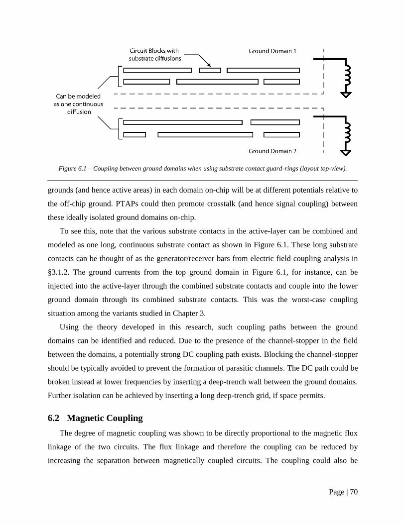
Page | 70
grounds (and hence active areas) in each domain on-chip will be at different potentials relative to
the off-chip ground. PTAPs could then promote crosstalk (and hence signal coupling) between
these ideally isolated ground domains on-chip.
To see this, note that the various substrate contacts in the active-layer can be combined and
modeled as one long, continuous substrate contact as shown in Figure 6.1. These long substrate
contacts can be thought of as the generator/receiver bars from electric field coupling analysis in
§3.1.2. The ground currents from the top ground domain in Figure 6.1, for instance, can be
injected into the active-layer through the combined substrate contacts and couple into the lower
ground domain through its combined substrate contacts. This was the worst-case coupling
situation among the variants studied in Chapter 3.
Using the theory developed in this research, such coupling paths between the ground
domains can be identified and reduced. Due to the presence of the channel-stopper in the field
between the domains, a potentially strong DC coupling path exists. Blocking the channel-stopper
should be typically avoided to prevent the formation of parasitic channels. The DC path could be
broken instead at lower frequencies by inserting a deep-trench wall between the ground domains.
Further isolation can be achieved by inserting a long deep-trench grid, if space permits.
6.2 Magnetic Coupling
The degree of magnetic coupling was shown to be directly proportional to the magnetic flux
linkage of the two circuits. The flux linkage and therefore the coupling can be reduced by
increasing the separation between magnetically coupled circuits. The coupling could also be
Figure 6.1 – Coupling between ground domains when using substrate contact guard-rings (layout top-view).

Page | 71
reduced by placing a metal shield over one or both of the coupled circuits. The effectiveness of
the metal shield was shown to be a function of its height above the circuit in question. While
using a shield can decrease the magnetic coupling, the added capacitance could decrease the
speed of digital circuitry, but this effect is minor relative to the benefits gained. However,
caution must be used as the metal shield (acting as a coplanar strip) could couple capacitively
with other nearby metals. Counter-winding inductors was also noted to be an effective method to
reduce the interaction between two planar spiral inductors when increasing their separation or
using metal shields is not practical.
Grounded metal shields can also reduce electric field coupling in addition to reducing
magnetic field coupling. As shown in Figure 6.2, if a grounded metal shield is positioned close to
the active-layer, a portion of the electric field lines may terminate on the shield. However, the
shield will not be able to completely divert all field lines, as shown in the Figure 6.2 as a single
field coupling through the substrate to the far substrate contact. The KSU Micro-Transceiver
Radio employs a grounded metal shield (shown in Figure 2.10) that may also help to reduce
electric field coupling from the digital synthesizer circuitry to the VCO, LNA and IF sections.
Further research is needed to characterize the positioning of such a metal shield relative to active
devices.
6.3 Bond Pads
The isolation strategies from the electric field coupling analysis were also applied to bond
pads. Similarly to the P+/N+ bars, the coupling between bond pads was found to be a function
of the impedance of the active-layer. Removing the active-layer under the pads with a deep-
trench grid provided a small but useful increase in isolation. Utilizing PTAP guard-rings further
Figure 6.2 – Metal shield reducing electric field coupling.

Page | 72
increased the isolation. A similar degree of isolation was achieved using a Metal-1 ground shield
under the pads, although doing so significantly increased the load capacitance of the bond pad. If
high-speed is a concern, using deep-trench grids under the pads trades isolation for a significant
decrease in load capacitance of the bond pad. Finally, placing a grounded bond pad between two
pads resulted in the same degree of isolation as using substrate contact guard-rings. However, if
this pad is bonded off-chip the extra ground bond wire will help decrease the ground-bounce
issues in that particular ground domain and may assist with electric field shielding between
bond-wires as well, to a moderate degree.

Page | 73
Appendix A - Spectrum Analyzer Data Acquisition with LabVIEW
The spectrum analyzer used to collect the magnetic coupling data did not have a floppy drive
or USB port to capture the power spectrum. However, the instrument does allow remote control
over GPIB. A custom LabVIEW program was designed to automate capturing the power
spectrum data from the instrument over GPIB. The data is automatically stored in a CSV file that
then can be plotted in MATLAB or similar graphing software.
The front panel of the LabVIEW program is shown in Figure A.1. In order to run the tool, the
LabVIEW 2010 Runtime Engine (or higher) and the Measurement and Automation Explorer
(MAX) 2010 (or higher) must both be installed. The instrument should be connected to the
computer via an appropriate GPIB interface. Ensure the GBIP interface and spectrum analyzer
are configured properly in MAX. On the instrument, set the desired settings such as the
amplitude, ResBW, VideoBW, etc. On the front panel of the tool select the GBIP address of the
spectrum analyzer under the VISA Resource Name dropdown, then set the start and stop
frequencies. Note that this particular spectrum analyzer has two frequency bands ranging from
0 – 2.921 GHz and from 2.921 – 22 GHz. The frequency span must lie completely within either
of these bands. If a full sweep from 0 – 22 GHz is required, data from the two bands can be
captured separately. To specify the output filename, select the yellow folder icon near the Path
textbox. Select the output directory and filename with extension (i.e. data.csv). Click the Capture
button to display the spectrum data on the Waveform plot and to generate and save the CSV file.
Figure A.1 – Front panel view of the Spectrum Analyzer Data Acquisition LabVIEW Tool
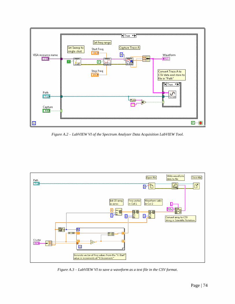
Page | 74
Figure A.2 – LabVIEW VI of the Spectrum Analyzer Data Acquisition LabVIEW Tool.
Figure A.3 – LabVIEW VI to save a waveform as a text file in the CSV format.
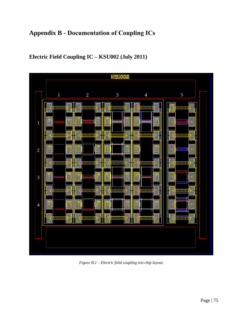
Page | 75
Appendix B - Documentation of Coupling ICs
Electric Field Coupling IC – KSU002 (July 2011)
Figure B.1 – Electric field coupling test chip layout.
1 2 3 4 5
1
2
3
4

Page | 76
Table B.1 – Cell descriptions of the electric field coupling test chip array.
Row Col Diffusion
Type
Bar
Separation
Channel-
Stopper
Deep
Trench
Metal
Fill
M1
Guard
Ring
PTAP
Guard
Ring
1 1 P+ 10 µm • •
2 1 P+ 100 µm • •
3 1 P+ 10 µm • • •
4 1 P+ 100 µm • • •
1 2 P+ 10 µm •
2 2 P+ 100 µm •
3 2 P+ 10 µm • •
4 2 P+ 100 µm • •
1 3 P+ 10 µm
2 3 P+ 100 µm
3 3 P+ 10 µm •
4 3 P+ 100 µm •
1 4 P+ 10 µm •
2 4 Blank cell for measurement floor
3 4 P+ 10 µm • •
4 4 P+ 100 µm • •
1 5 N+ 10 µm •
2 5 N+ 10 µm • •
3 5 N+ 100 µm • •
4 5 N+ 100 µm
Figure B.2 – Photograph of the electric field test array IC.
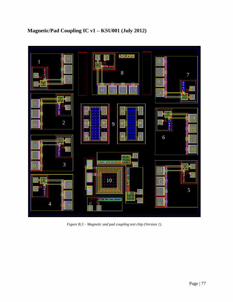
Page | 77
Magnetic/Pad Coupling IC v1 – KSU001 (July 2012)
Figure B.3 – Magnetic and pad coupling test chip (Version 1).
1
2
3
4
5
6
7 8
9
10
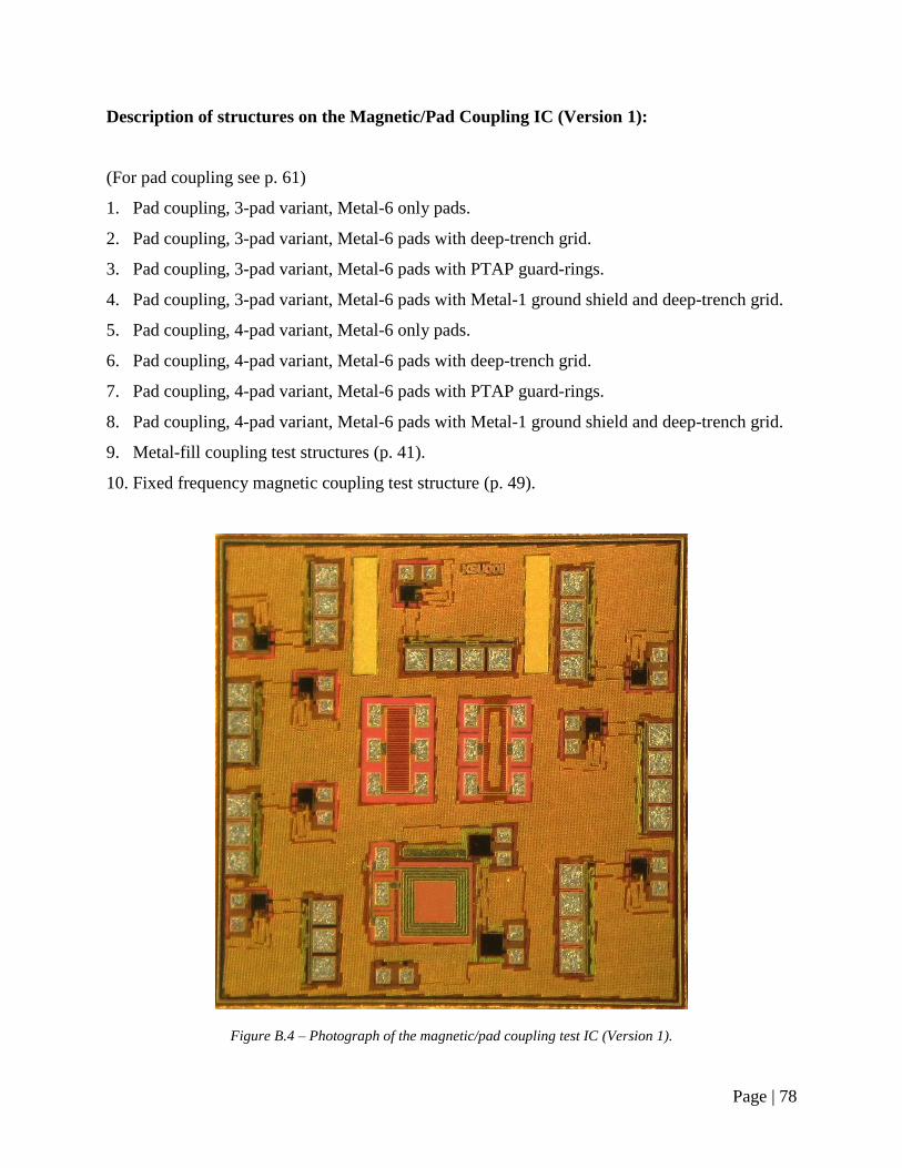
Page | 78
Description of structures on the Magnetic/Pad Coupling IC (Version 1):
(For pad coupling see p. 61)
1. Pad coupling, 3-pad variant, Metal-6 only pads.
2. Pad coupling, 3-pad variant, Metal-6 pads with deep-trench grid.
3. Pad coupling, 3-pad variant, Metal-6 pads with PTAP guard-rings.
4. Pad coupling, 3-pad variant, Metal-6 pads with Metal-1 ground shield and deep-trench grid.
5. Pad coupling, 4-pad variant, Metal-6 only pads.
6. Pad coupling, 4-pad variant, Metal-6 pads with deep-trench grid.
7. Pad coupling, 4-pad variant, Metal-6 pads with PTAP guard-rings.
8. Pad coupling, 4-pad variant, Metal-6 pads with Metal-1 ground shield and deep-trench grid.
9. Metal-fill coupling test structures (p. 41).
10. Fixed frequency magnetic coupling test structure (p. 49).
Figure B.4 – Photograph of the magnetic/pad coupling test IC (Version 1).
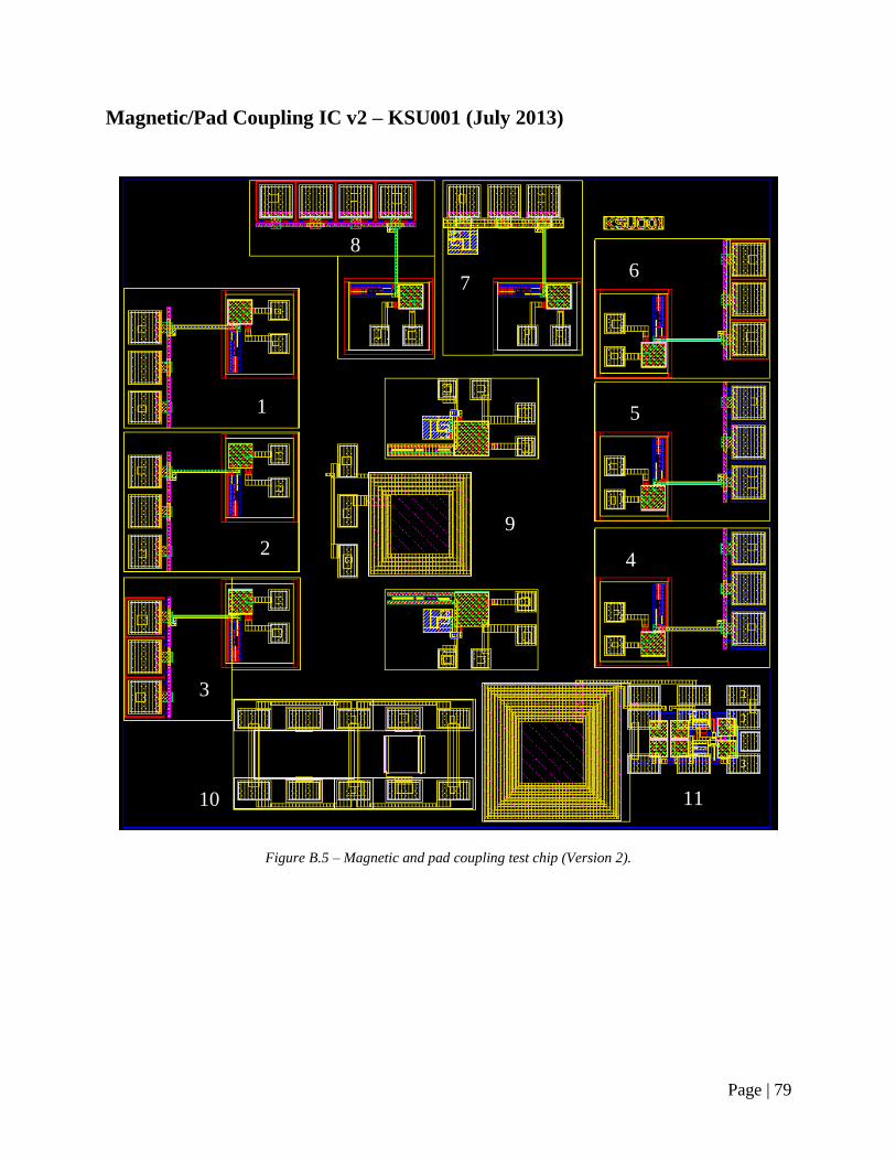
Page | 79
Magnetic/Pad Coupling IC v2 – KSU001 (July 2013)
Figure B.5 – Magnetic and pad coupling test chip (Version 2).
1
2
3
5
6 7
8
9
4
10 11

Page | 80
Description of structures on the Magnetic/Pad Coupling IC (Version 2):
Note: at the time of writing, this chip was still in manufacturing.
(For pad coupling see p. 66)
1. Pad coupling: 3-pad variant, Metal-6 only pads.
2. Pad coupling, 3-pad variant, Metal-6 pads with deep-trench grid.
3. Pad coupling, 3-pad variant, Metal-6 pads with PTAP guard-rings.
4. Pad coupling, 3-pad variant, Metal-6 pads with Meta- 1 ground shield under pads.
5. Pad coupling, 3-pad variant, Metal-6 pads with Metal-1 ground shield and deep-trench grid.
6. Pad coupling, 3-pad variant, Metal-6 pads only but with floating VDD bus bar.
7. Pad coupling, 3-pad variant, Metal-6 pads with VDD bus bar, ESD protection diodes and ESD
clamp.
8. Pad coupling, 4-pad variant, Metal-6 pads with PTAP guard-rings.
9. Variable frequency magnetic coupling test structure (p. 58).
10. Additional P+/N+ bars for electric field coupling (p. 47).
11. Low-noise amplifier (LNA) for an unrelated project.
Page | 81
References
[1] L. S. Miller and W. Kuhn, “Biosensor Networks and Telecommunication Subsystems for
Long-Duration Missions, EVA Suits, and Robotic Precursor Scout Missions,” Wichita State
University, NASA EPSCoR Project NNX11AM05A, 2011.
[2] W. Kuhn, N. E. Lay, E. Grigorian, D. Nobbe, I. Kuperman, J. Jeon, K. Wong, Y. Tugnawat,
and X. He, “A Microtransceiver for UHF Proximity Links Including Mars Surface-to-Orbit
Applications,” Proc. IEEE, vol. 95, no. 10, pp. 2019–2044, 2007.
[3] T. J. Sobering, KSU Body Area Network Board. 2012.
[4] “Controlling Radiated EMI Through PCB Stack-up | EE Times,” EETimes. [Online].
Available: http://www.eetimes.com/document.asp?doc_id=1214998. [Accessed: 24-Sep-
2013].
[5] A. Hodges, “Investigation of Antennas and Energy Harvesting Methods for use with a UHF
Microtransceiver in a Biosensor Network,” Masters Thesis, Kansas State University, 2013.
[6] B. Carter, “Circuit Board Layout Techniques,” in Op Amps for Everyone, Texas
Instruments, 2008.
[7] H. Zumbahlen, “Staying Well Grounded,” Analog Devices: Analog Dialouge, Jun-2012.
[Online]. Available: http://www.analog.com/library/analogdialogue/archives/46-
06/staying_well_grounded.html. [Accessed: 06-Sep-2013].
[8] R. Reeder, “Techniques for High Speed ADC PCB Layout,” Analog Devices. [Online].
Available: http://www.analog.com/static/imported-files/application_notes/AN-1142.pdf.
[Accessed: 23-Sep-2013].
[9] “Power Supply and Ground Design for a WiFi Transceiver,” Maxim Integrated, 23-Sep-
2005. [Online]. Available: http://www.maximintegrated.com/app-notes/index.mvp/id/3630.
[Accessed: 23-Sep-2013].
[10] “Decoupling Techniques.” Analog Devices, Mar-2009.
[11] B. J. LaMeres, “Characterization of a Printed Circuit Board Via,” Masters Thesis,
University of Colorado at Colorado Springs, 2000.
[12] T. H. Lee, “Coplanar Waveguide (CPW) and Coplanar Strip (CPS),” in Planar Microwave
Engineering, 1st ed., Cambridge, 2004, pp. 168–170.

Page | 82
[13] R. Naylor, “Study of flip-chip and beam-lead microcircuit assemblies,” Proc. Inst. Electr.
Eng., vol. 116, no. 10, pp. 1621–1627, 1969.
[14] A. J. Joseph, J. D. Gillis, M. Doherty, P. J. Lindgren, R. A. Previti-Kelly, R. M. Malladi, P.-
C. Wang, M. Erturk, H. Ding, E. G. Gebreselasie, M. J. McPartlin, and J. Dunn, “Through-
silicon vias enable next-generation SiGe power amplifiers for wireless communications,”
IBM J. Res. Dev., vol. 52, no. 6, pp. 635–648, 2008.
[15] M. Yamaguchi, S. Muroga, Y. Endo, W. Kodate, K. Yoshikawa, Y. Sasaki, and Makoto
Nagata, “Performance of integrated magnetic thin film noise suppressor applied to CMOS
noise test chips,” in Microwave Conference (EuMC), 2011 41st European, 2011, pp. 49–52.
[16] K. Yamamoto, M. Fujishima, and K. Hoh, “Optimization of shield structures in analog
integrated circuits,” in Proceedings of the 2003 International Symposium on Circuits and
Systems, 2003. ISCAS ’03, 2003, vol. 1, pp. I–753–I–756 vol.1.
[17] T. Yamashita, S. Komori, K. Horita, Y. Kawasaki, Y. Inoue, and T. Nishimura, “Highly
reliable double well in thin p/sup -/ on p/sup +/ epitaxial wafer for logic-embedded
DRAM,” in Electron Devices Meeting, 1997. IEDM ’97. Technical Digest., International,
1997, pp. 673–676.
[18] “LOCOS - The new layer cake mix,” IEEE Spectr., vol. 8, no. 7, pp. nil4–nil4, 1971.
[19] Y. Niitsu, S. Taguchi, K. Shibata, H. Fuji, Y. Shimamune, H. Iwai, and K. Kanzaki,
“Latchup-free CMOS structure using shallow trench isolation,” in Electron Devices
Meeting, 1985 International, 1985, vol. 31, pp. 509–512.
[20] R. B. Merrill, W. M. Young, and K. Brehmer, “Effect of substrate material on crosstalk in
mixed analog/digital integrated circuit,” in Electron Devices Meeting, 1994. IEDM ’94.
Technical Digest., International, 1994, pp. 433–436.
[21] D. Kosaka, Makoto Nagata, Y. Hiraoka, I. Imanishi, M. Maeda, Y. Murasaka, and A. Iwata,
“Isolation strategy against substrate coupling in CMOS mixed-signal/RF circuits,” in 2005
Symposium on VLSI Circuits, 2005. Digest of Technical Papers, 2005, pp. 276–279.
[22] G. A. Rezvani and J. Tao, “Substrate isolation in 0.18um CMOS technology,” in
Proceedings of the 2005 International Conference on Microelectronic Test Structures,
2005. ICMTS 2005, 2005, pp. 131–136.
[23] W. Xu and E. G. Friedman, “On-chip test circuit for measuring substrate and line-to-line
coupling noise,” IEEE J. Solid-State Circuits, vol. 41, no. 2, pp. 474–482, 2006.

Page | 83
[24] W. Muth, “Matrix method for latch-up free demonstration in a triple-well bulk-silicon
technology,” IEEE Trans. Nucl. Sci., vol. 39, no. 3, pp. 396–400, 1992.
[25] J. R. Baker, “Standard Cell Frame,” in CMOS Circuit Design, Layout, and Simulation, 3rd
ed., CMOS Circuit Design, Layout, and Simulation, 2010, pp. 97–98.
[26] M. L. Alles, “Thin film SOI emerges,” IEEE Spectr., vol. 34, no. 6, pp. 37–45, 1997.
[27] J. E. Lilienfield, “Method and Apparatus for Controlling Electric Currents,” 1,745,175.
[28] I. Lagnado, P. R. De la Houssaye, W. B. Dubbelday, S. J. Koester, R. Hammond, J. O. Chu,
J. A. Ott, P. M. Mooney, L. Perraud, and K. A. Jenkins, “Silicon-on-sapphire for RF Si
systems 2000,” in 2000 Topical Meeting on Silicon Monolithic Integrated Circuits in RF
Systems, 2000. Digest of Papers, 2000, pp. 79–82.
[29] V. Jaju, “SOI Technology,” 2004. [Online]. Available:
http://archives.ece.iastate.edu/archive/00000046/. [Accessed: 14-Jul-2013].
[30] S. S. Eaton and B. Lalevic, “The effect of a floating substrate on the operation of silicon-
on-sapphire transistors,” IEEE Trans. Electron Devices, vol. 25, no. 8, pp. 907–912, 1978.
[31] J.-P. Raskin, A. Viviani, D. Flandre, and J. Colinge, “Substrate crosstalk reduction using
SOI technology,” IEEE Trans. Electron Devices, vol. 44, no. 12, pp. 2252–2261, 1997.
[32] J. S. Hamel, S. Stefanou, M. Bain, B. M. Armstrong, and H. S. Gamble, “Substrate
crosstalk suppression capability of silicon-on-insulator substrates with buried ground planes
(GPSOI),” IEEE Microw. Guid. Wave Lett., vol. 10, no. 4, pp. 134–135, 2000.
[33] M. Rahim, B.-Y. Hwang, and J. Foerstner, “Comparison of Soi Versus Bulk Silicon
Substrate Crosstalk Properties for Mixed-Mode IC’s,” in SOI Conference, 1992. IEEE
International, 1992, pp. 170–171.
[34] K. Joardar, “Comparison of SOI and junction isolation for substrate crosstalk suppression in
mixed mode integrated circuits,” Electron. Lett., vol. 31, no. 15, pp. 1230–1231, 1995.
[35] Y. Hiraoka, S. Matsumoto, and T. Sakai, “New substrate-crosstalk reduction structure using
SOI substrate [for one-chip transceiver IC],” in SOI Conference, 2001 IEEE International,
2001, pp. 107–108.
[36] Z. Guoyan, L. -Huailin, H. Ru, Z. Xing, and W. Yangyuan, “The simulation analysis of
cross-talk behavior in SOI mixed-mode integrated circuits,” in 6th International
Conference on Solid-State and Integrated-Circuit Technology, 2001. Proceedings, 2001,
vol. 2, pp. 916–919 vol.2.

Page | 84
[37] M. Pfost, P. Brenner, T. Huttner, and A. Romanyuk, “An experimental study on substrate
coupling in bipolar/BiCMOS technologies,” IEEE J. Solid-State Circuits, vol. 39, no. 10,
pp. 1755–1763, 2004.
[38] F. Farbiz and E. Rosenbaum, “Guard Ring Interactions and their Effect on CMOS Latchup
Resilience,” in Electron Devices Meeting, 2008. IEDM 2008. IEEE International, 2008, pp.
1–4.
[39] W. B. Kuhn, “Loss mechanisms and quality factor improvement for inductors in high-
resistivity SOI processes,” in 2012 IEEE 12th Topical Meeting on Silicon Monolithic
Integrated Circuits in RF Systems (SiRF), 2012, pp. 29–32.
[40] X. Dong, I. Seo, and W. Kao, “New metal fill considerations for nanometer technologies,”
in ASIC, 2005. ASICON 2005. 6th International Conference On, 2005, vol. 2, pp. 802–805.
[41] V. Shilimkar, “Metal Fill Considerations for On-chip Interconnects and Spiral Inductors,”
Oregon State University, 2009.
[42] A. Balasinski and J. Cetin, “Intelligent Fill Pattern and Extraction Methodology for SoC,”
in The 6th International Workshop on System-on-Chip for Real-Time Applications, 2006,
pp. 156–159.
[43] P. Descamps, C. Barbier-Petot, C. Biard, and S. Bardy, “Performance comparison of
substrate coupling effect between silicon and SOI substrates in RF-CMOS technology,”
Electron. Lett., vol. 42, no. 20, pp. 1151–1152, 2006.
[44] J. Ankarcrona, L. Vestling, K.-H. Eklund, and J. Olsson, “Low resistivity SOI for substrate
crosstalk reduction,” IEEE Trans. Electron Devices, vol. 52, no. 8, pp. 1920–1922, 2005.
[45] S. Y. Huang, “Loss Tangent.” MIT, 17-Feb-2012.
[46] J. Krupka, J. Breeze, A. Centeno, N. Alford, T. Claussen, and L. Jensen, “Measurements of
Permittivity, Dielectric Loss Tangent, and Resistivity of Float-Zone Silicon at Microwave
Frequencies,” IEEE Trans. Microw. Theory Tech., vol. 54, no. 11, pp. 3995–4001, 2006.
[47] G. Ghione and C. Naldi, “Analytical formulas for coplanar lines in hybrid and monolithic
MICs,” Electron. Lett., vol. 20, no. 4, pp. 179–181, 1984.
[48] S. Gevorgian and H. Berg, “Line Capacitance and Impedance of Coplanar-Strip
Waveguides on Substrates with Multiple Dielectric Layers,” in Microwave Conference,
2001. 31st European, 2001, pp. 1–4.

Page | 85
[49] R. S. Muller and T. I. Kamis, “Electronic Devices for Integrated Circuits,” 3rd ed., New
York: Wiley, 2003, pp. 140–150.
[50] K. Joardar, “A simple approach to modeling cross-talk in integrated circuits,” IEEE J.
Solid-State Circuits, vol. 29, no. 10, pp. 1212–1219, 1994.
[51] U. Gogineni, H. Li, J. A. del Alamo, S. L. Sweeney, J. Wang, and B. Jagannathan, “Effect
of Substrate Contact Shape and Placement on RF Characteristics of 45 nm Low Power
CMOS Devices,” IEEE J. Solid-State Circuits, vol. 45, no. 5, pp. 998–1006, 2010.
[52] W. B. Kuhn, F. W. Stephenson, and A. Elshabini-Riad, “A 200 MHz CMOS Q-enhanced
LC bandpass filter,” IEEE J. Solid-State Circuits, vol. 31, no. 8, pp. 1112–1122, 1996.
[53] J. R. Baker, “Current-Starved VCO,” in CMOS Circuit Design, Layout, and Simulation, 3rd
ed., Wiley-IEEE Press, 2010, pp. 561–565.
[54] Y.-W. Hsiao and M.-D. Ker, “Ultra Low-Capacitance Bond Pad for RF Applications in
CMOS Technology,” in 2007 IEEE Radio Frequency Integrated Circuits (RFIC)
Symposium, 2007, pp. 303–306.
[55] S. Lam, P. K. T. Mok, P. K. Ko, and M. Chan, “High-isolation bonding pad design for
silicon RFIC up to 20 GHz,” IEEE Electron Device Lett., vol. 24, no. 9, pp. 601–603, 2003.
[56] M.-D. Ker and J.-J. Peng, “Investigation on device characteristics of MOSFET transistor
placed under bond pad for high-pin-count SOC applications,” IEEE Trans. Components
Packag. Technol., vol. 27, no. 3, pp. 452–460, 2004.