reconfiguration-based built-in self-test - lancaster...
TRANSCRIPT

Reconfiguration-Based Built-In Self-Testfor Analogue Front-End Circuits
A. Lechner1, A. Richardson1 & B. Hermes2,1 Faculty of Applied Sciences, Lancaster University, Lancaster, LA1 4YR, UK.
2 Philips Semiconductors, Millbrook Industrial Estate, Southampton, SO15 ODJ, UK.
AbstractPrevious work has shown that it is feasible to implement afully digital test evaluation function to realise partial self-test on an automatic gain control circuit (AGC). Thispaper extends the technique to INL, DNL, offset & gainerror testing of analogue to digital converters (ADC's). Italso shows how the same function can be used to test anAGC / ADC pair. An extension to full self-test is alsoproposed by the on-chip generation of input stimulithrough reconfiguration of existing functions.
1 Introduction
Design for Test (DfT) and Built-In Self-Test (BIST)for analogue and mixed signal circuits have received thegrowing attention of industry in order to alleviateincreasing test related difficulties. Testability is predictedto become a primary design specification and has to beaddressed in the early design stages, as escalating test time& costs need to be controlled and quality levels improved.In addition to improved fabrication testability, BIST offersan extension towards in-field verification while alsoallowing test re-use and providing a promising approach toautomate mixed signal test generation.
This paper describes an extension of an on-chip, fullydigital test evaluation function [1,2] to an AGC(Automatic Gain Control circuit) ADC pair. On-chip rampstimulus generation technique are proposed that are basedon reconfiguration of available mixed signal cells toimplement a full BIST function.
2 State-of-the-Art in Analogue and Mixed-Signal Built-In Self-Test
Currently, functional testing is performed onanalogue circuits after wafer processing, where every IC ischecked against critical specifications [3, 4]. Theoptimisation of such circuit specific test programs isdifficult and expensive. Generic DfT guidelines andpractical mixed signal BIST which can be applied in theearly design stages could pave the way to satisfyingindustrial demands for the use of digital only testers [5, 6]and a structural methodology for test program generationand optimisation. Increasing test costs, aggressivedemands on time to market, and the need to improveproduct quality currently drive this change in testphilosophy.
Various mixed signal BIST approaches have beenpublished, such as ABIST [7], adcBIST [8], AUBIST [9],BIST for converters on a CODEC [10], HBIST [11],MADBIST [12], OBIST [13], & TBIST [14]; additionallya review on mixed signal BIST can be found in [15]. Anoverview of defect oriented testing and DfT optimisationof mixed signal ICs is presented in [4, 16, 17, 18].
3 Analogue Front-End Circuit
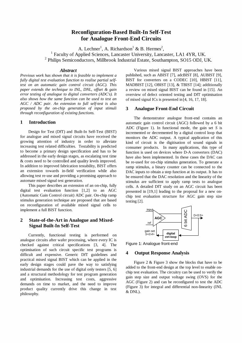
The demonstrator analogue front-end contains anautomatic gain control circuit (AGC) followed by a 6 bitADC (Figure 1). In functional mode, the gain set S isincremented or decremented by a digital control loop thatmonitors the ADC output. A typical application of thiskind of circuit is the digitisation of sound signals inconsumer products. In many applications, this type offunction is used on devices where D-A converters (DAC)have also been implemented. In these cases the DAC canbe re-used for on-chip stimulus generation. To generate aramp stimulus, a binary counter can be connected to theDAC inputs to obtain a step function at its output. It has tobe ensured that the DAC resolution and the linearity of thestimulus are sufficient to apply ramp tests to analoguecells. A detailed DfT study on an AGC circuit has beenpresented in [19,1] leading to the proposal for a new on-chip test evaluation structure for AGC gain step sizetesting [2].
6 bi
t AD
C
gain setS<0:4>
D<0:5>
input
refAGC
digitalctrl-loop
Figure 1: Analogue front-end
4 Output Response Analysis
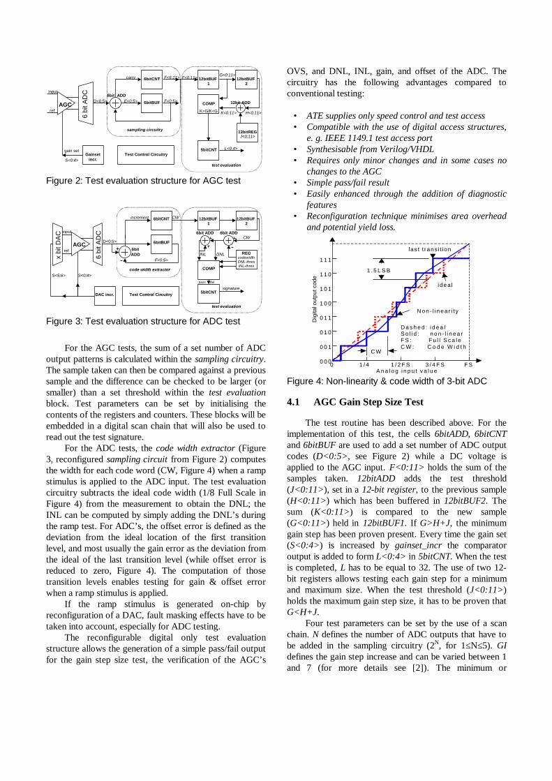
Figure 2 & Figure 3 show the blocks that have to beadded to the front-end design at the top level to enable on-chip test evaluation. The circuitry can be used to verify thegain step size and output voltage swing (OVS) for theAGC (Figure 2) and can be reconfigured to test the ADC(Figure 3) for integral and differential non-linearity (INL& DNL).
6 bi
t AD
C6bitCNT
6bitBUF
gain set
S<0:4>
D<0:5> E<0:5>
F<0:11>F<6:11>
12bitREG
12bitBUF1
COMP
K>G/K<G
J<0:11>
G<0:11>
6bit ADD
12bit ADD
K<0:11>
5bitCNT L<0:4>Gainset
incr.Test Control Circuitry
F<0:5>
sampling circuitry
carry
input
refAGC
test evaluation
12bitBUF2
H<0:11>
Figure 2: Test evaluation structure for AGC test
6 bi
t AD
C
6bitBUF
S<0:4>
D<0:5>
CW
REG
12bitBUF1
COMP
codewidthDNL-thresINL-thres
6bitADD
6bit ADD
5bitCNTsignature
DAC incr. Test Control Circuitry
F<0:5>
code width extractor
increment
input
refAGC
test evaluation
12bitBUF2
6bit ADD
INL DNL
pass fail
CW
x bi
t DA
C
S<5:6>
6bitCNT
Figure 3: Test evaluation structure for ADC test
For the AGC tests, the sum of a set number of ADCoutput patterns is calculated within the sampling circuitry.The sample taken can then be compared against a previoussample and the difference can be checked to be larger (orsmaller) than a set threshold within the test evaluationblock. Test parameters can be set by initialising thecontents of the registers and counters. These blocks will beembedded in a digital scan chain that will also be used toread out the test signature.
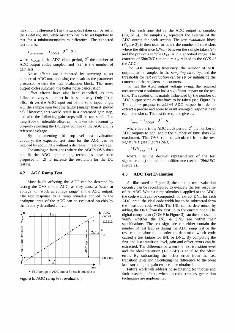
For the ADC tests, the code width extractor (Figure3, reconfigured sampling circuit from Figure 2) computesthe width for each code word (CW, Figure 4) when a rampstimulus is applied to the ADC input. The test evaluationcircuitry subtracts the ideal code width (1/8 Full Scale inFigure 4) from the measurement to obtain the DNL; theINL can be computed by simply adding the DNL’s duringthe ramp test. For ADC’s, the offset error is defined as thedeviation from the ideal location of the first transitionlevel, and most usually the gain error as the deviation fromthe ideal of the last transition level (while offset error isreduced to zero, Figure 4). The computation of thosetransition levels enables testing for gain & offset errorwhen a ramp stimulus is applied.
If the ramp stimulus is generated on-chip byreconfiguration of a DAC, fault masking effects have to betaken into account, especially for ADC testing.
The reconfigurable digital only test evaluationstructure allows the generation of a simple pass/fail outputfor the gain step size test, the verification of the AGC’s
OVS, and DNL, INL, gain, and offset of the ADC. Thecircuitry has the following advantages compared toconventional testing:
• ATE supplies only speed control and test access• Compatible with the use of digital access structures,
e. g. IEEE 1149.1 test access port• Synthesisable from Verilog/VHDL• Requires only minor changes and in some cases no
changes to the AGC• Simple pass/fail result• Easily enhanced through the addition of diagnostic
features• Reconfiguration technique minimises area overhead
and potential yield loss.
A n a l o g i n p u t v a l u e
1 1 1
1 1 0
1 0 1
1 0 0
0 1 1
0 1 0
0 0 1
0 0 00 1 / 4 1 / 2 F S 3 / 4 F S F S
idea l
Dig
ital o
utpu
t cod
eN o n - l i n e a r i t y
1 . 5 L S B
C W
D a s h e d : i d e a lS o l i d : n o n - l i n e a rF S : F u l l S c a l eC W : C o d e W i d t h
las t t rans i t ion
Figure 4: Non-linearity & code width of 3-bit ADC
4.1 AGC Gain Step Size Test
The test routine has been described above. For theimplementation of this test, the cells 6bitADD, 6bitCNTand 6bitBUF are used to add a set number of ADC outputcodes (D<0:5>, see Figure 2) while a DC voltage isapplied to the AGC input. F<0:11> holds the sum of thesamples taken. 12bitADD adds the test threshold(J<0:11>), set in a 12-bit register, to the previous sample(H<0:11>) which has been buffered in 12bitBUF2. Thesum (K<0:11>) is compared to the new sample(G<0:11>) held in 12bitBUF1. If G>H+J, the minimumgain step has been proven present. Every time the gain set(S<0:4>) is increased by gainset_incr the comparatoroutput is added to form L<0:4> in 5bitCNT. When the testis completed, L has to be equal to 32. The use of two 12-bit registers allows testing each gain step for a minimumand maximum size. When the test threshold (J<0:11>)holds the maximum gain step size, it has to be proven thatG<H+J.
Four test parameters can be set by the use of a scanchain. N defines the number of ADC outputs that have tobe added in the sampling circuitry (2N, for 1≤N≤5). GIdefines the gain step increase and can be varied between 1and 7 (for more details see [2]). The minimum or
maximum difference (I) in the samples taken can be set inthe 12-bit register, while MinMax has to be set high/low totest for a minimum/maximum difference. The expectedtest time is:
322 ⋅⋅= NADCclkstgainstepte tt ,
where tADCclk is the ADC clock period, 2N the number ofADC output codes sampled, and “32” is the number ofgain sets.
Noise effects are eliminated by summing a setnumber of ADC outputs using the result as the parameterprocessed within the test evaluation block. The moreoutput codes summed, the better noise cancellation.
Offset effects have also been cancelled, as theyinfluence every sample set in the same way. Only if theoffset drives the ADC input out of the valid input range,will the sample sum become faulty (smaller than it shouldbe). However, this would result in a decreased gain step,and also the following gain steps will be too small. Themagnitude of tolerable offset can be taken into account byproperly selecting the DC input voltage of the AGC and itsreference voltage.
By implementing this top-level test evaluationcircuitry, the expected test time for the AGC can bereduced by about 70% without a decrease in test coverage.
For analogue front-ends where the AGC’s OVS doesnot fit the ADC input range, techniques have beenproposed in [2] to increase the resolution for the DCtesting.
4.2 AGC Ramp Test
Most faults affecting the AGC can be detected bytesting the OVS of the AGC, as they cause a ‘stuck atvoltage’ or ‘stuck at voltage range’ at the AGC output.The test response to a ramp stimulus applied to theanalogue input of the AGC can be evaluated on-chip bythe circuitry described above.
time
AG
C o
utpu
tvol
tage
ADCoutput
AD
C in
put r
ange
000000
111111
tS
∆f I,I-1 FI-1
FI
Fi: Average of ADC output for each time slot tS
Vos
Vos
8tS
Figure 5: AGC ramp test evaluation
For each time slot tS, the ADC output is sampled(Figure 5). The samples Fi represent the average of theADC output for each section. The test evaluation block(Figure 2) is then used to count the number of time slotswhere the difference (∆fI,I-1) between the sample taken (FI)and the previous sample (FI-1) is in a specified range. Thecontents of 5bitCNT can be directly related to the OVS ofthe AGC.
The ADC sampling frequency, the number of ADCoutputs to be sampled in the sampling circuitry, and thethresholds for test evaluation can be set by initialising thecontents of the registers and counters.
To test the AGC output voltage swing, the requiredmeasurement resolution has a significant impact on the testtime. The resolution is mainly influenced by the number ofADC output samples that have to be taken (see Figure 5).The authors propose to add 64 ADC outputs in order toextract a precise and noise tolerant averaged response overeach time slot ts. The test time can be give as:
stt NADCclkramp ⋅⋅= 2 ,
where tADCclk is the ADC clock period, 2N the number ofADC outputs to add, and s the number of time slots (32maximum). The OVS can be calculated from the testsignature L (see Figures 2&3):
jlOVSmeas ⋅=where l is the decimal representative of the test
signature and j the minimum difference (set in 12bitREG,Figure 2).
4.3 ADC Test Evaluation
As illustrated in Figure 3, the on-chip test evaluationcircuitry can be reconfigured to evaluate the test responseof the ADC. When a ramp stimulus is applied to the ADC,the code width can be computed. To extract DNL for eachADC input, the ideal code width has to be subtracted formthe measured code width. The INL can be determined byadding the DNL from the first up to the current code. Thedigital comparator (COMP in Figure 3) can then be used toverify whether the INL & DNL are within theirspecifications. The test signature can either contain thenumber of test failures during the ADC ramp test or thetest can be aborted in order to determine which codecaused a test failure for INL or DNL. By computing thefirst and last transition level, gain and offset errors can beextracted. The difference between the first transition leveland the ideal transition (1/2 LSB) is equal to the offseterror. By subtracting the offset error from the lasttransition level and calculating the difference to the ideallast transition, the gain error can be obtained.
Future work will address noise filtering techniques andfault masking effects when on-chip stimulus generationtechniques are implemented.
5 Reconfiguration-Based Ramp StimulusGeneration
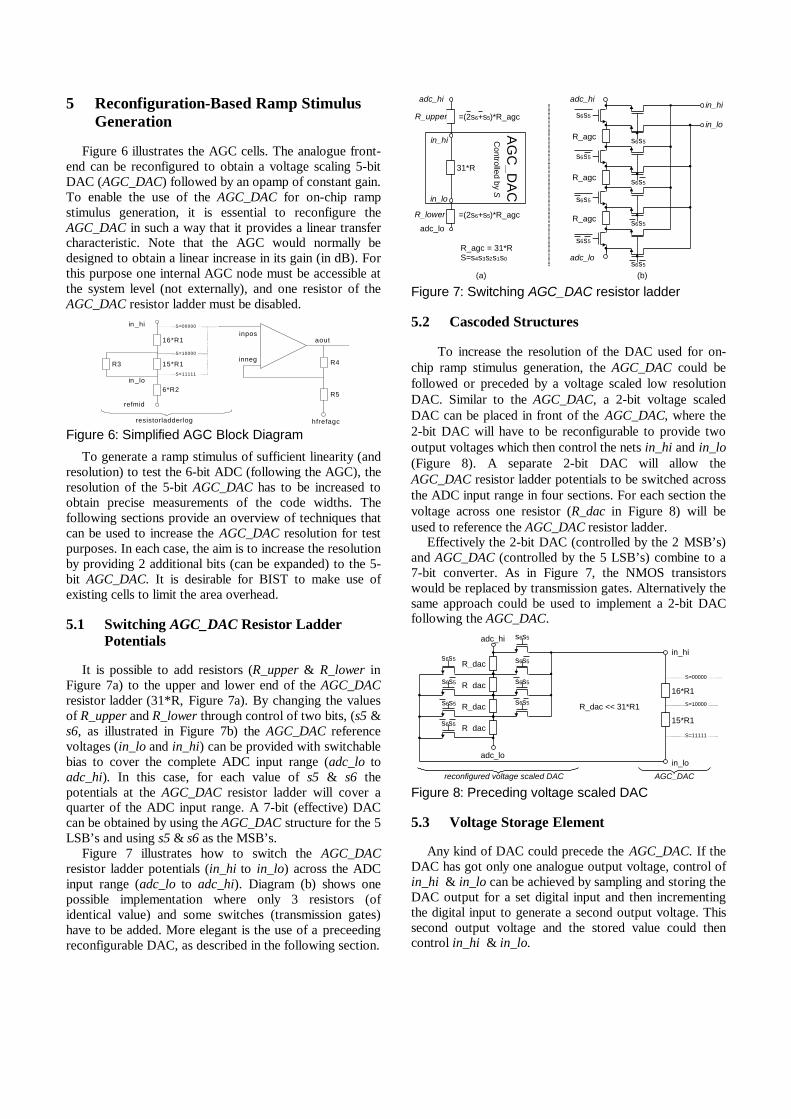
Figure 6 illustrates the AGC cells. The analogue front-end can be reconfigured to obtain a voltage scaling 5-bitDAC (AGC_DAC) followed by an opamp of constant gain.To enable the use of the AGC_DAC for on-chip rampstimulus generation, it is essential to reconfigure theAGC_DAC in such a way that it provides a linear transfercharacteristic. Note that the AGC would normally bedesigned to obtain a linear increase in its gain (in dB). Forthis purpose one internal AGC node must be accessible atthe system level (not externally), and one resistor of theAGC_DAC resistor ladder must be disabled.
inpos
R4
R5
inneg
aout
hfrefagc
16*R1
in _hi
refmid
15*R1
6*R2
R3S=11111
S=00000
S=10000
resistorladderlog
in _lo
Figure 6: Simplified AGC Block Diagram
To generate a ramp stimulus of sufficient linearity (andresolution) to test the 6-bit ADC (following the AGC), theresolution of the 5-bit AGC_DAC has to be increased toobtain precise measurements of the code widths. Thefollowing sections provide an overview of techniques thatcan be used to increase the AGC_DAC resolution for testpurposes. In each case, the aim is to increase the resolutionby providing 2 additional bits (can be expanded) to the 5-bit AGC_DAC. It is desirable for BIST to make use ofexisting cells to limit the area overhead.
5.1 Switching AGC_DAC Resistor LadderPotentials
It is possible to add resistors (R_upper & R_lower inFigure 7a) to the upper and lower end of the AGC_DACresistor ladder (31*R, Figure 7a). By changing the valuesof R_upper and R_lower through control of two bits, (s5 &s6, as illustrated in Figure 7b) the AGC_DAC referencevoltages (in_lo and in_hi) can be provided with switchablebias to cover the complete ADC input range (adc_lo toadc_hi). In this case, for each value of s5 & s6 thepotentials at the AGC_DAC resistor ladder will cover aquarter of the ADC input range. A 7-bit (effective) DACcan be obtained by using the AGC_DAC structure for the 5LSB’s and using s5 & s6 as the MSB’s.
Figure 7 illustrates how to switch the AGC_DACresistor ladder potentials (in_hi to in_lo) across the ADCinput range (adc_lo to adc_hi). Diagram (b) shows onepossible implementation where only 3 resistors (ofidentical value) and some switches (transmission gates)have to be added. More elegant is the use of a preceedingreconfigurable DAC, as described in the following section.
s6s5
s6s5
s6s5
31*R
in_hi
R_agc = 31*RS=s4s3s2s1s0
in_lo
adc_hi
adc_lo
=(2s6+s5)*R_agc
=(2s6+s5)*R_agc
in_hi
in_los6s5
adc_hi
s6s5adc_lo
s6s5
s6s5
s6s5
(b)(a)A
GC
_DA
C
R_upper
R_lower R_agc
Controlled by S
R_agc
R_agc
Figure 7: Switching AGC_DAC resistor ladder
5.2 Cascoded Structures
To increase the resolution of the DAC used for on-chip ramp stimulus generation, the AGC_DAC could befollowed or preceded by a voltage scaled low resolutionDAC. Similar to the AGC_DAC, a 2-bit voltage scaledDAC can be placed in front of the AGC_DAC, where the2-bit DAC will have to be reconfigurable to provide twooutput voltages which then control the nets in_hi and in_lo(Figure 8). A separate 2-bit DAC will allow theAGC_DAC resistor ladder potentials to be switched acrossthe ADC input range in four sections. For each section thevoltage across one resistor (R_dac in Figure 8) will beused to reference the AGC_DAC resistor ladder.
Effectively the 2-bit DAC (controlled by the 2 MSB’s)and AGC_DAC (controlled by the 5 LSB’s) combine to a7-bit converter. As in Figure 7, the NMOS transistorswould be replaced by transmission gates. Alternatively thesame approach could be used to implement a 2-bit DACfollowing the AGC_DAC.
s6s5
16*R1
in_hi
in_lo
15*R1
S=11111
S=00000
S=10000
AGC_DAC
adc_hi
adc_lo
R_dac
R_dac
R_dac
s6s5
s6s5
s6s5
s6s5
s6s5
s6s5
s6s5
reconfigured voltage scaled DAC
R_dac
R_dac << 31*R1
Figure 8: Preceding voltage scaled DAC
5.3 Voltage Storage Element
Any kind of DAC could precede the AGC_DAC. If theDAC has got only one analogue output voltage, control ofin_hi & in_lo can be achieved by sampling and storing theDAC output for a set digital input and then incrementingthe digital input to generate a second output voltage. Thissecond output voltage and the stored value could thencontrol in_hi & in_lo.

5.4 Use of ATE
If the AGC_DAC inputs in_hi and in_lo are bothaccessible, DC voltages could be provided from theexternal ATE (Automatic Test Equipment) in the sameway that they would be provided by an on-chip DAC. Alsoaccessible inputs of a preceding DAC could be used toincrease the combined DAC-AGC_DAC resolution. Thewhole ramp stimulus generator can be followed by a RCnetwork to improve the linearity of the ramp even further.
6 Conclusions
A partial BIST structure has been designed toimplement on-chip test evaluation for an AGC gain steptest, the verification of the AGC output voltage swing andverification of ADC specifications (INL, DNL, gain,offset). This study has shown that digital solutions topartial self-test are feasible for analogue front-ends of thistype and that in many cases reconfiguration of digitalcontrol loops may well be a highly optimal BISTenhancement.
The test evaluation circuitry can be implemented atthe macro level using digital logic only and hence willrequire minimal design effort if synthesis techniques areused. This solution has been shown to improve the AGCtest time by up to 70% without any degradation in faultcoverage. Where the proposed solution is implemented inparallel with careful design for fault tolerance, very highfault coverage is feasible.
To extend the partial BIST to a full BIST foranalogue front-ends, a number of techniques have beenproposed to generate a ramp stimulus on-chip. Thesetechniques involve re-using existing components witheither DC signals from the tester or from a separate on-chip DAC. The use of these techniques can improve theaccuracy of the BIST ramp stimuli.
7 References 1 A.Lechner, A. Richardson, A.Perkins, M.Zwolinski &
B.Hermes: Design for testability strategies for a highperformance automatic gain control circuit, IMSTW98.
2 A.Lechner, J.Ferguson, A.Richardson & B.Hermes: A digitalpartial built-in self-test structure for a high performanceautomatic gain control circuit, Proc. Design, Automation &Test in Europe, pp. 232-238, 1999.
3 A. Grochowski, D. Bhattacharya, T.R. Viswanathan & K.Laker: Integrated circuit testing, IEEE Trans. on Circuits andSystems II: Analog and Digital Signal Processing, vol. 44,no. 8, pp. 610-633, 1997.
4 K. Baker, A.M Richardson & A.P. Dorey: Mixed signal test -techniques, applications and demands, IEE Proc.-CircuitsDevices Systems, vol. 143, no. 6, Dec. 1996.
5 F.G.M. de Jong: Analogue system testability: an industrialperspective, AMATIST, ESPRIT Open WorkshopProceedings, Twente, May 1997.
6 S. Sunter: Mixed-Signal BIST - Does industry need it?, Proc.
3rd IEEE International Mixed Signal Workshop, Tutorial 2,Seattle, June 1997.
7 C.-L. Wey & S. Krishnan: Built-in self-test (BIST) structuresfor analogue circuit fault diagnosis with current test data,IEEE Trans. on Instrumentation and Measurement, vol. 41,no. 4, pp. 535-539, 1992.
8 S. Sunter & N. Nagi: A Simplified Polynominal-fittingalgorithm for DAC and ADC BIST, Proc. International TestConference 1997, pp389-395.
9 S. Mir, M. Lubaszewski & B. Courtois: Unified built-in self-test for fully differential analogue circuits, Journal ofElectronic Testing: Theory and Applications, vol. 9, no. 1-2,pp. 135-151, 1996.
10 E. Teraoka, T. Kengaku, I. Yasui, K. Ishikawa, T. Matsuo, H.Wakada, N. Sakashita, Y. Shimazu & T. Tokada: A built-inself-test for ADC and DAC in a single chip speech CODEC,IEEE Proc. International Test Conference, 791-796, 1993.
11 M. J. Ohletz: Hybrid built-in self-test (HBIST) for mixedanalogue/digital ICs', Proc. European Design & TestConference, pp. 307-16, 1991.
12 M. F. Toner & G. W. Roberts: A frequency response,harmonic distortion test for BIST of a sigma-delta ADC,IEEE Trans. on Circuits and Systems-II, vol. 43, no. 8, pp.608-613, 1996.
13 K. Arabi & B. Kaminska: Oscillation built-in self test(OBIST) scheme for functional and structural testing ofanalog and mixed-signal integrated circuits, Proc.International Test Conference, paper 31.4, pp786-796, Nov1st-6th, Washington DC, 1997.
14 M. Slamani, B. Kaminska & G. Quesnal: An integratedapproach for analog circuit testing with a minimum numberof detected parameters, IEEE Proc. International TestConference, pp. 631-640, 1994.
15 L. S. Milor: A tutorial introduction to research on analog andmixed-signal circuit testing, IEEE Trans. On Circuits andSystems-II, vol. 45, no. 10, pp. 1389-1407, 1998
16 C.-J. Wang & C.-L. Wey: Efficient testability designmethodologies for analog/mixed-signal integrated circuits,3rd Int. Mixed Signal Testing Workshop, Seattle, pp. 68-74,June 1997.
17 A.Richardson, A.Lechner, T.Olbrich: Design for testabilitystrategies for mixed signal & analogue designs - from layoutto system, Proc. Int. Conf. on Electonics, Circuits andSystems, vol. 2, pp. 425-432, 1998
18 Y.-R. Shieh & C.-W. Wu: Control and observation structuresfor analog circuits, IEEE Design & Test of Computers, pp.56-64, Apr-Jun 1998
19 A. Lechner, A. Richardson, B. Hermes, & M. Ohletz: Adesign for testability study on a high performance automaticgain control circuit, Proceedings of the IEEE VLSI TestSymposium, pp. 376-385, 1998, Monterey, California.