realization of physical hybrid arq indicator channel … · long term evolution ... by block...
TRANSCRIPT

Procedia Engineering 30 ( 2012 ) 426 – 434
1877-7058 © 2011 Published by Elsevier Ltd.doi: 10.1016/j.proeng.2012.01.881
Available online at www.sciencedirect.com
International Conference on Communication Technology and System Design 2011
Realization of Physical Hybrid ARQ Indicator Channel for LTE using FPGA
S.Syed Ameer Abbasa, R.Lakshmi Prabaa, S.J.Thiruvengadamb, a* a,Mepco Schlenk Engineering College,Sivakasi-626005, India bThiagarajar College of Engineering, Madurai-625015, India
Abstract
Realization of transmitter and receiver architecture for LTE is the major research work being carried out by implementation experts. There are four Control channels available in LTE for both uplink and downlink. The uplink control channel is PUCCH. The downlink control channels are PDCCH, PCFICH and PHICH. The Physical Hybrid Automatic Repeat Request (ARQ) Indicator Channel(PHICH) is the control channel which carries the acknowledgement (ACK/NACK), denoted as Hybrid ARQ Indicator(HI).These control channels play a key role in the correct decoding of the payload information. The HI is used to indicate the ACK for data sent using Physical Uplink Shared Channel (PUSCH), and is important for the system performance. In this paper, the realization of architecture for the PHICH are done using FPGA, where the main aim is to estimate the HI correctly in the receiver side. The simulations are done using Modelsim and are implemented in Xilinx Spartan 3E kit.
© 2011 Published by Elsevier Ltd. Selection and/or peer-review under responsibility of ICCTSD 2011
Keywords: LTE, FPGA, HI, ARQ, PUSCH ;
1. Introduction
Long Term Evolution (LTE) is a Fourth generation wireless broadband technology, which is capable of providing high peak data rates (100 Mbps downlink and 50 Mbps uplink),multi antenna support, reduced cost, wide range of bandwidth(from 1.4 MHZ upto 20 MHZ), backward compatibility with existing 2G and 3G networks, increased spectrum efficiency and peak data rates at cell edges[1-3]. All these criteria are satisfied by the efficient usage of the control channels. The LTE physical layer is a highly efficient means of conveying both data and control information between an enhanced base station(e-Node B) and mobile user equipment (UE). The LTE physical layer uses OFDM as the access technology, QAM as the modulation scheme and MIMO concepts. LTE differs from its predecessors by using OFDM along with MIMO antennas. OFDM is selected ,owing to its suitability for MIMO transmission and reception, resistance of its symbol structure to multi path delay spread, no need of equalization etc[4].
The downlink physical channels correspond to a set of resource elements carrying information originating from the higher layers. There are six physical downlink channels available namely, Physical Downlink Shared Channel (PDSCH), Physical Broadcast Channel(PBCH), Physical Multicast Channel (PMCH), Physical Control Format
* Syer Ameed Abbas. Tel.: 94436 60172 ; fax: 04562 235111. E-mail address: [email protected].
Open access under CC BY-NC-ND license.
Open access under CC BY-NC-ND license.

427 S. Syed Ameer Abbas et al. / Procedia Engineering 30 ( 2012 ) 426 – 434
Indicator Channel (PCFICH), Physical Downlink Control Channel (PDCCH), Physical Hybrid ARQ Indicator Channel (PHICH) [1].The first three channels are the data channels. The PDSCH carries the payload and PBCH broadcast the cell specific information. The PMCH is used for broadcasting and multicasting information from multiple cells. The latter three channels are the control channels, where PDCCH is the main control channel carrying the downlink scheduling assignments and the uplink scheduling grants. The PCFICH carries the control Format Indicator(CFI), which provides the number of OFDM symbols used by the PDCCH channel. The PHICH carries the hybrid – ARQ ACK / NACK Indicator (HI). The downlink physical signals are Reference signal and the Synchronization signal. The reference signals are of three types namely Cell Specific reference signals, MBSFN reference signals, UE-specific reference signals. The synchronization signals are primary synchronization signal and secondary synchronization signal and they provide the information of physical layer cell identity, which ranges from 0 to 503[1].
LTE supports both Time Division (TDD) and Frequency Division Duplexing (FDD). In this paper FDD is adopted.. The frame structure for FDD used in this realization is shown in Fig.1. Each downlink frame lasts for 10 ms and consists of 10 sub frames. Each sub frame consists of 2 slots. Each slot consists of seven OFDM symbols [1].LTE specification provides capacity enhancing features such as link adaptation , Hybrid Automatic Repeat Request(H-ARQ) etc. So, control channel design and structure plays a lead role in the correct detection and interpretation of the payload information. Hence, successful decoding of the control channels is needed to ensure the overall link and system performance[4].
The objective of this paper is to propose transmitter and receiver architecture for PHICH channel and to implement the architectures using FPGA. The proposed architectures can be optimized using VLSI DSP techniques of folding, Unfolding, retiming etc.
The rest of the paper is organized as follows. In Section II, a brief discussion of PHICH channel is done, followed by block diagram and modelling of the transmitter and receiver architecture is done. In Section III, assumptions are provided and the architectures for the PCFICH transmitter and receiver are proposed. Section IV, provides the simulation results and discussion. Section V, contains some concluding remarks.
2. Physical Hybrid ARQ Indicator Channel
The PHICH channel carries the channel coded HARQ Indicator (HI) codeword. The enodeB sends a HARQ indicator to the UE to indicate positive acknowledgement (ACK) or negative acknowledgement (NACK) for data sent using the uplink shared channel. The HARQ Indicator of ‘1’ represents ACK and ‘0’ represents NACK. Multiple PHICHs are mapped to the same set of resource elements (REs). This set of REs constitutes a PHICH group. The PHICHs within a PHICH group are separated through different orthogonal sequences.
2.1 PHICH Transmitter
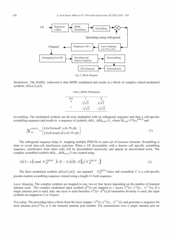
Channel Coding The 1 bit ACK/NACK Indicator undergoes repetition coding to form a HARQ indicator codeword made up of three bits,<b0, b1, b2>.
Table.1.Repetition coding
HARQ HARQ Indicator Codeword 0-Nagative Acknowledgement <0,0,0> 1-Positive Acknowledgement <1,1,1>
428 S. Syed Ameer Abbas et al. / Procedia Engineering 30 ( 2012 ) 426 – 434
Fig. 2. Block Diagram
Modulation. The HARQ codeword is then BSPK modulated and results in a block of complex-valued modulated symbols, z(0),z(1),z(2).
Table.2.BPSK MOdulation
Scrambling. The modulated symbols are bit-wise multiplied with an orthogonal sequence and then a cell-specific scrambling sequence and results in a sequence of symbols, d(0),...d(Msymb-1) , where Msymb=3*NSF
PHICH and
efixdCyclicforExtende
efixyclicforNormalCN
PHICH
SF Pr2
Pr4 (1)
The orthogonal sequence helps in mapping multiple PHICHs to same set of resource elements. Scrambling is done to avoid inter-cell interference rejection. When a UE descrambles with a known cell specific scrambling sequence, interference from other cells will be descrambled incorrectly and appear as uncorrelated noise. The complex scrambled symbols d(0),...,d(Msymb-1) are created using
PHICHSF
PHICHSF NiZicNiwid 21mod (2)
The three modulated symbols z(0),z(1),z(2) are repeated PHICHSFN times and scrambled. C is a cell-specific
pseudo-random scrambling sequence created using a length-31 Gold sequence.
Layer Mapping. The complex symbols are mapped to one, two or four layers depending on the number of transmit antenna used. The complex modulated input symbols d(0)(i) are mapped to v layers x(0)(i), x(1)(i),... x(v-1)(i), If a single antenna port is used, only one layer is used therefore x(0)(i)= d(0)(i),If transmitter diversity is used, the input symbols are mapped to 2 or 4 layers.
Precoding. The precoding takes a block from the layer mapper x(0)(i), x(1)(i),... x(v-1)(i), and generates a sequence for each antenna port,y(p)(i), p is the transmit antenna port number .For transmission over a single antenna port no
b(i) I Q 0
21 211
21 21
Repetitioncoding
BPSKModulation Scrambling
Layer mapping and Precoding
Mapping to RE s
Spreading using orthogonal
Channel
Demapping from RE Decoding and Delayer mapping
Descrambling
DemodulationHI Estimation
1/0
429 S. Syed Ameer Abbas et al. / Procedia Engineering 30 ( 2012 ) 426 – 434
processing is carried out y(p)(i)= x(0)(i). In two antenna port precoding, an alamouti scheme is used for precoding, which defines the relationship between input and output as shown in eqn.(3).In the Alamouti Scheme, two consecutive symbols x(0)(i) and x(1)(i) are transmitted in parallel using two antennas with the following mapping. (*) is the complex conjugate .
ix
ix
ix
ix
j
j
j
j
iy
iy
iy
iy
1
0
1
0
1
0
1
0
Im
Im
Re
Re
001
010
010
001
21
12
12
2
2
(3)
As any two columns in the precoding matrix are orthogonal, the two symbols, x(0)(i) and x(1)(i)can be separated
at the UE. For four antenna port case, precoding depends on the index nPHICH
group.If in
PHICH
groupis even for an
extended cyclic prefix In this scheme two consecutive symbols are transmitted in parallel in two symbol periods
using antennas zero and two.If inPHICH
groupis odd for an extended cyclic prefix,in this scheme two consecutive
symbols are transmitted in parallel in two symbol periods using antennas one and three.
Mapping to Resource Elements. The number of ODFM symbols used to carry the PHICH depends on either normal or extended PHICH duration. A normal PHICH duration causes the PHICH to be present in only the first OFDM symbol. In general an extended PHICH duration causes the PHCH to be present in the first three OFDM symbols.
Resource Group Alignment. For FDD case, the number of PHICH groups is constant in all sub frames and is given by,
efixdCyclicforExtendeNN
efixyclicforNormalCNN
DLRBg
DLRBgPHICH
groupN Pr82
Pr8 (4)
Where 2,1,21,61gN is provided by higher layers. The index of the PHICH group NPHICH
groupranges from
0 to 1NPHICH
group.
2.2 PHICH Receiver
Received Signal. The received signal is processed as follows. First the cyclic prefix is removed, and then FFT is taken, followed by resource element demapping. The output representing the ith resource element group and kth
receiver antenna is given by,
ki
M
n
M
nnn
nnn
nkiki uxw
Pjxw
Pw
Pxhy ,
2 1
~~
11
1,, 222 (5)
Where i=1,2,3 and K is the number of antennas, kiy , is an Mx1 vector, nP and~
nP ,n=1,2,...M are the power levels
of the M orthogonal codes (for normal cyclic prefix case), 1,11x is the data bit value of the desired user
HI, nx and kih , is an Mx1 complex channel frequency response vector. It is assumed that the desired HI channel to
be decoded uses the first orthogonal code denoted as 1w .The second and third terms denote the remaining 2M-1

430 S. Syed Ameer Abbas et al. / Procedia Engineering 30 ( 2012 ) 426 – 434
spreading codes used for the other HI channels within a PHICH group. The term kiu , denotes the thermal noise,
which is modelled as circularly symmetric zero mean complex Gaussian with covariance IuuE uH
kiki2
,, .
HI Estimation. The Maximum Likelihood Decoding for HI Estimation is given by,
K
kkzz
1
(6)
Where k is the number of antennas at the UE receiver and
3
1,
ikik zz (7)
Where 1
^*,,, ,Re whyz kikiki (8)
So for HI Estimation K
k ikiki
mwhyHI
1
3
11
^*,,
1,0,Remaxarg (9)
Where kikiki ehh ,,,
^ and kie , is the estimation error, which is uncorrelated with kih , and zero –mean complex
Gaussian with covariance given by Ie2 .The inner product is *
1
, i
N
ii yxyx . The received signal kiy , is element
by element multiplied with the conjugate of estimated channel frequency response vector. The resultant product then undergoes inner product with the first spreading sequence w1.The real part of the result is alone extracted. This is repeated for each resource element group, i=1,2,3 and the results are summed up. This is the process done for one antenna port. Similarly for k number of antenna ports, the results are found and then the argument maximum among them is selected as the estimated as the Hybrid Indicator (HI).For ideal channel estimation, then due to the orthogonality property of the spreading codes, no interference is introduced to 1w from the other HI channels within a PHICH group.
3. Proposed Architecture for PHICH Transmitter and Receiver
Table.3.Assumptions
Parameter Assumption Channel Bandwidth (MHz) 1.4 Number of Physical Resource Blocks 6 Number of occupied subcarriers 73 Cyclic Prefix Normal Number of OFDM symbols per sub frame 14 (7 in each slot) Frame Structure Type I(FDD) HI(bits) 1 Gold Sequence(bits) 12 Modulated Symbol(bits) 16 Channel Rayleigh fading channel frequency response vector(hk) 16 bit 16X1 vector Conjugate of channel frequency response vector(hk
*) 16 bit 16X1 vector Noise vector(uk) 16 bit 16X1 vector
3.1 Transmitter Architecture
The transmitter architecture is presented in fig.3.The transmitter architecture consists of Repetition Coding, Modulation, Scrambling, layer mapping, precoding and mapping to Resource Elements..The input is the 1 bit HI

431 S. Syed Ameer Abbas et al. / Procedia Engineering 30 ( 2012 ) 426 – 434
value, whether 0 or 1.Here, it is assumed that a stream of 32 bits, stored in a shift register as input. For one shift, one ack/ nack is provided as input. The1 bit value is converted to 3 bit value by repetition coding. These 3 bits form the HI codeword. For scrambling process, gold sequence generation is needed. The gold sequence is produced by using the 2 sequences X1 and X2.The X1 sequence is a predefined sequence, which is “100000000000”. The 12 bits of X2 sequence is assumed, since it varies according to the applications. Then these 2 sequences are XOR ed to get the gold sequence, which is also a 12 bit value. The gold sequence is stored in a shift register, which shifts one bit per clock cycle. Here, the scrambling operation is performed after the modulation. The modulation for the PHICH channel is always BPSK. So, each bit will be converted into a BPSK modulated symbol. Then scrambling is done by using the code word and the gold sequence. The resultant scrambled symbols are 12 in number(d(0) to d(11)).These 12 symbols are then layer mapped, precoded.The12 complex modulated symbols are then layer mapped to one, two or four layers based on the information from higher layer.Z1 is the output if one antenna is selected.Z2,Z3 are outputs if 2 antennas are selected and Z4,Z5,Z6,Z7 if 4 antennas are selected. For single antenna case precoding , output will be streamed without any change. For 2 and 4 antenna cases, first incoming symbol is
multiplied with 2/1 .Then the original symbols and the conjugate signals are produced by sign change, and are arranged in the order to be transmitted. They are mapped to the resource grid positions allotted to them in the first OFDM symbol of first slot. The positions are(in case of 1.4 MHZ bandwidth) viz. 7,8,10,11,25,26,28,29,49,50,52,53RE positions.Then each layer or antenna produces a resource grid structure carrying the symbols. The modulated symbol is multiplied with the complex channel frequency response vector hk, which is also represented as a 16 bit value. The resultant is a 32 bit value. Then noise which is represented using 16 bits is added. Thus the resultant signal yk is a 32 bit value.
Fig. 3.PHICH Transmitter Architecture

432 S. Syed Ameer Abbas et al. / Procedia Engineering 30 ( 2012 ) 426 – 434
3. 2 Receiver Architecture
The received signal is first demapped from the resource elements in the grid. Only in 12 positions of first OFDM symbol, HI value is available. Decoding is done to get the original symbols, by selecting the strongest signals. The delayer mapping is just retrieving back the 12 symbols in order. The receiver architecture is presented in fig.4. The 12 received signals are used to estimate the HI value transmitted. It is known that, there are only two possibilities of signal transmitted, namely 0 or 1(HI-0 or HI-1 ).So, the demodulated signal will be one among the two, which is used in the estimation of the HI, by finding argument maximum among ttwo results. The received signal is yk and is multiplied with the estimated value of conjugate of the complex channel frequency response vector hk
*,element by element. Then this resultant term undergoes inner product with thew1 sequence used to spread the code. The inner product is done using the formula in section 2.For all the elements the multiplication is done and the results are accumulated, and the result is a 64 bit value. The real part of the accumulated value alone is taken, which is a 32 bit value. Then among the two results, the codeword which has the maximum argument value is detected as the HI.
Fig. 4.PHICH Receiver Architecture
4. Results and Discussion
The architecture for the PHICH channel transmitter upto mapping to resource elements and receiver to estimate HI are designed and implemented in FPGA. The simulations are done using Modelsim and synthesized using Xilinx 8.1i and Spartan 3E kit is used for implementation. The programming are done using Verilog HDL.
For the transmitter side, the inputs are clock and the one bit HI value (0 or 1).Fig. 10 provides the simulation output for transmitter. In fig.10,one bit HI input is given. The repetition coding produces 3 bit output, which on modulation produces 48 bit output. The modulated symbols are represented using 16 bits. The modulated symbols are multiplied with channel response and then noise is added. After modulation, scrambling is done,using orthogonal sequences.From the synthesis report, the number of multipliers used is four, which are all 16x16-bit multiplier. The adders used are three 32 bit adders . The number of comparators used is two. The symbols are then layermapped, precoded and mapped to resource elements. The delay incurred in the transmitter is 5.021ns.
433 S. Syed Ameer Abbas et al. / Procedia Engineering 30 ( 2012 ) 426 – 434
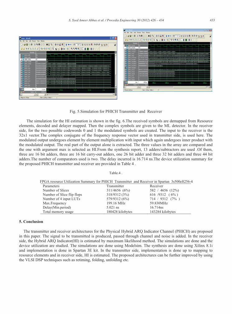
Fig. 5.Simulation for PHICH Transmitter and Receiver
The simulation for the HI estimation is shown in the fig. 6.The received symbols are demapped from Resource elements, decoded and delayer mapped. Then the complex symbols are given to the ML detector. In the receiver side, for the two possible codewords 0 and 1 the modulated symbols are created. The input to the receiver is the 32x1 vector.The complex conjugate of the frequency response vector used in transmitter side, is used here. The modulated output undergoes element by element multiplication with input which again undergoes inner product with the modulated output. The real part of the output alone is extracted. The three values in the array are compared and the one with argument max is selected as HI.From the synthesis report, 13 adders/subtractors are used .Of them, three are 16 bit adders, three are 16 bit carry-out adders, one 26 bit adder and three 32 bit adders and three 44 bit adders.The number of comparators used is two. The delay incurred is 16.714 ns.The device utilization summary for the proposed PHICH transmitter and receiver are provided in Table 4 .
Table.4 .
FPGA resource Utilization Summary for PHICH Transmitter and Receiver in Spartan 3s500eft256-4 Parameters Transmitter Receiver Number of Slices 311/4656 (6%) 582 / 4656 (12%) Number of Slice flip flops 318/9312 (3%) 616 /9312 ( 6% ) Number of 4 input LUTs 579/9312 (6%) 714 / 9312 (7% ) Max.Frequency 199.16 MHz 59.830MHz Delay(Min.period) 5.021 ns 16.714ns Total memory usage 180428 kilobytes 143284 kilobytes
5. Conclusion
The transmitter and receiver architectures for the Physical Hybrid ARQ Indicator Channel (PHICH) are proposed in this paper. The signal to be transmitted is produced, passed through channel and noise is added. In the receiver side, the Hybrid ARQ Indicator(HI) is estimated by maximum likelihood method. The simulations are done and the device utilization are studied. The simulations are done using Modelsim. The synthesis are done using Xilinx 8.1i and implementation is done in Spartan 3E kit. In the transmitter side, implementation is done up to mapping to resource elements and in receiver side, HI is estimated. The proposed architectures can be further improved by using the VLSI DSP techniques such as retiming, folding, unfolding etc.

434 S. Syed Ameer Abbas et al. / Procedia Engineering 30 ( 2012 ) 426 – 434
References
[1] 3GPP TS 36.211, “ Evolved Universal Terrestrial Radio Access (E- UTRA)”, Physical Channels and Modlation (Release 8). [2] 3GPP TS36.212, “Evolved Universal Terrestrial Radio Access(E-UTRA)”, Multiplexing and Channel Coding (Release 8). [3] 3GPP TS36.306, “Evolved Universal Terrestrial Radio Access(E-UTRA)”, User Equipment radio access capabilities (Release 8). [4] S.J.Thiruvengadam, Louay M. A. Jalloul, “Performance Analyis of the 3GPP-LTE Physical Control Channels,” EURASIP Journal
onWireless Communications and Networking, vol.2010, Nov.2010, Article ID.914934, 10 pages. [5] R.Love, R.Kuchibhotla, A.Ghosh et al., “Downlink control channel design for 3GPP LTE”, in proceedings of IEEE wireless
communication and Networking Conference(WCNC’08), April 2008, Las Vegas, Nev, USA, pp.813-818.