realization and optimization of organic electronic devices ... · pdf filerealization and...
TRANSCRIPT

UNIVERSITÀ DEGLI STUDI DI NAPOLI FEDERICO II
International PhD Program on:
Novel Technologies for Materials,
Sensors and Imaging
XXIV cycle
Realization and optimization of organic
electronic devices manufactured by
innovative technique: inkjet printing
Immacolata Angelica Grimaldi
Tutors: Dr. Fulvia Villani
Dr. Antonio Cassinese


…to angels…


This thesis describes the research activity of I.A.Grimaldi during the three years of
the International PhD program on Novel Technologies for Materials, sensors and
Imaging (TIMSI – XXIV cicle)- University of Naples “Federico II” (Italy). The
activity was performed at ENEA – Portici Research Center in “Nanomaterials and
Device Technology” was supported by Italian Ministry of Economic Development in
the framework of the Operating Agreement with ENEA for the Research on the
Electric System and Technologies and Research for the application of polymers in
electronics devices TRIPODE project financed by the University and Research
Ministry.


____________________________________________________________________
TABLE OF CONTENTS
Introduction ........................................................................................................- 1 - Chapter 1 - Inkjet printing for the organic electronics.......................- 5 - Inkjet printing technology for the organic electronics .............................................- 5 -
1 Inkjet printing techniques..................................................................................- 6 - 1.1 Continuous Ink Jet printing techniques..........................................................- 7 -
1.1.1 Binary Continuous Inkjet ...................................................................- 7 - 1.1.2 Multiple Deflection System ...............................................................- 7 - 1.1.3 Hertz Continuous Inkjet .....................................................................- 8 -
1.2 Drop on Demand Inkjet printing techniques..................................................- 9 - 1.2.1 Thermal Inkjet printing ......................................................................- 9 - 1.2.2 Piezoelectric Inkjet printing .............................................................- 10 - 1.2.3 Electrostatic Inkjet Printing..............................................................- 12 - 1.2.4 Focused Acoustic Inkjet Printing.....................................................- 12 - 1.2.5 Piezo-Acoustic Inkjet Printing .........................................................- 13 -
1.3 Fluid dynamic principles..............................................................................- 15 - 1.4 Ink formulation.............................................................................................- 17 - 1.5 Ink-substrate system.....................................................................................- 19 -
1.5.1 Wetting of the substrate ...................................................................- 20 - 1.5.2 “Coffee-ring” effect .........................................................................- 22 - 1.5.3 Marangoni effect ..............................................................................- 23 -
1.6 Organic electronics.......................................................................................- 24 - 1.6.1 Charge transport in organic semiconductors....................................- 25 -
1.7 Organic electronic applications....................................................................- 30 - 1.7.1 Conductive polymer materials for sensing applications ..................- 31 - 1.7.2 Optical grade polymers for optical structures..................................- 31 - 1.7.3 Organic semiconductor for transistor applications ..........................- 32 - 1.6.5 Polymer blend for solar cell applications.........................................- 34 -
Bibliography.......................................................................................................- 35 - Chapter 2 - Sensors........................................................................................- 39 -
2.1 Conductive polymer nanocomposites ..........................................................- 40 - 2.1.1 Swelling mechanism ........................................................................- 40 -
2.2 Geometry role in the sensor performances...................................................- 41 - 2.2.1 Sensing film: ink formulation and characterizations .......................- 41 - 2.2.2 Sensor device assembly ...................................................................- 43 - 2.2.3 Electrical characterization under analyte vapours............................- 46 -
2.3 Flexible substrates for sensor device fabrication .........................................- 50 - 2.3.1 Printing optimization by surface treatments ....................................- 51 - 2.3.2 Sensor device fabrication .................................................................- 53 -

Introduction ___________________________________________________________________
____________________________________________________________________
2.3.3 Electrical characterization to acetone vapours .................................- 55 - 2.3.4 Electrical characterization to ethanol vapours .................................- 57 -
2.4 Summary ..................................................................................................... - 58 - Bibliography...................................................................................................... - 60 -
Chapter 3 – Optical structures.................................................................. - 63 -
3.1 Introduction to polymer microstructuring ................................................... - 65 - 3.2 Inkjet etching of polymer surface................................................................ - 66 -
3.2.1 PI structured by NMP.......................................................................- 67 - 3.2.2 PS structured by TOL.......................................................................- 71 - 3.2.3 PS structured by TOL:NMP.............................................................- 72 - 3.2.3.1 Optical characterization via Mach-Zehnder interferometer .......... - 74 -
3.3 Applications of polymer microstructures to optoelectronic devices........... - 77 - 3.3.1 PI structured by NMP in mould applications ...................................- 78 - 3.3.2 PS structured by TOL as textured substrates in OLED applications- 78 - 3.3.2.1 OLEDs: introduction and improvements ...................................... - 78 - 3.3.2.2 OLED device fabrication .............................................................. - 79 - 3.3.2.3 Interference effects in an optical cavity ........................................ - 81 - 3.3.3 PS structured by TOL:NMP as microlenses OLED applications ....- 85 -
3.4 Microlens fabrication via additive method.................................................. - 88 - 3.4.1 Microlens fabrication .......................................................................- 89 - 3.4.2 Microlens characterization ...............................................................- 90 -
3.5 Summary ..................................................................................................... - 95 - Bibliography...................................................................................................... - 97 -
Chapter 4 – Organic Field Effect Transistor..................................... - 100 -
4.1 Introduction of OFETs .............................................................................. - 101 - 4.2 Current-voltage characteristics of OFETs................................................. - 101 - 4.3 n-type OFETs based on Perylene Diimide derivatives ............................. - 104 -
4.3.1 OFETs fabrication ..........................................................................- 106 - 4.3.2 Morphological characterization......................................................- 108 - 4.4.3 Electrical characterization ..............................................................- 113 -
4.5 Summary ................................................................................................... - 116 - Bibliography.................................................................................................... - 118 -
Chapter 5 – Organic Solar Cells............................................................. - 120 -
5.1 Introduction of OPV.................................................................................. - 121 - 5.2 Photovoltaic working principle ................................................................. - 121 - 5.3 OPV solar cells based on P3HT:PCBM blend.......................................... - 125 -
5.3.1 OPV fabrication..............................................................................- 126 - 5.3.2 Morphological characterization......................................................- 128 - 5.3.3 Electrical characterization ..............................................................- 130 -
5.4 Summary ................................................................................................... - 132 - Bibliography.................................................................................................... - 133 -

Conclusions......................................................................................................- 135 - Acknowledgement.........................................................................................- 139 - Glossary............................................................................................................- 141 -


____________________________________________________________________
____________________________________________________________________ i
LIST OF FIGURES
Figure 1.1 Diagram of the available inkjet printing technologies [1]. .....................- 6 - Figure 1.2 Schematic illustration of a binary-deflection continuous inkjet system [1].-
7 - Figure 1.3 Schematic illustration of a multiple-deflection continuous inkjet [1]. ...- 8 - Figure 1.4 Schematic illustration of Hertz continuous inkjet [1].............................- 8 - Figure 1.5 Schematic illustration of a thermal inkjet [1]. ........................................- 9 - Figure 1.6 Schematic illustration of a roof-shooter design (left) and edge-shooter
design (right) of a thermal inkjet device [1]...................................................- 10 - Figure 1.7 Schematic illustration of (a) squeeze mode, (b) shear mode, (c) push mode
and (d) bend mode of a piezoelectric inkjet printing [1]................................- 11 - Figure 1.8 Schematic illustration of a Focused Acoustic Inkjet printer.................- 12 - Figure 1.9 (a) Schematic illustration of a Microdrop piezo-acoustic inkjet printhead
(b) picture of a AD-K-501 pipette; (c) picture of a MD-K-130 printhead with holder and reservoir........................................................................................- 13 -
Figure 1.10 Image of the inkjet printing equipment at ENEA Portici. ..................- 15 - Figure 1.11 Drop images of a stable condition (a), formation of filament (b) and
formation of satellite droplet (c). ...................................................................- 19 - Figure 1.12 Schema of droplet wetting on a solid surface.....................................- 20 - Figure 1.13 Illustration of “coffee-stain” effect. Evaporation rate (represented by
upward arrows) is highest at the edges of a printed droplet resulting in an accumulation of the solute at the periphery at the end of the drying process. .- 22 -
Figure 1.14 Illustration of “Marangoni effect”. The diffusive flow (“coffee-stain” effect) is directed from the centre to the edge of the printed droplet. If mixture of high- and low- boiling point solvents is employed an inward Marangoni flow can be generate, inducing a balance of material at the centre of the dried droplet.........................................................................................................................- 23 -
Figure 1.15 Schematic representation of Energy bands for insulators, semiconductors and conductors. ..............................................................................................- 26 -
Figure 1.16 Electronic structure of carbon in its ground state. ..............................- 26 - Figure 1.17 Electronic structure of the sp3 hybridization. .....................................- 27 - Figure 1.18 Molecular orbitals of sp hybridization................................................- 27 - Figure 1.19 (a) sp2-hybridized orbital of a carbon atom; (b) molecular orbitals of two
double bonded carbon atom forming π bonds and σ bonds. ..........................- 28 - Figure 1.20 Schema of organic field effect transistor. ...........................................- 33 - Figure 1.21 Examples of chemical structure of (a) p-type and (b) n-type conjugated
polymer semiconductors. ...............................................................................- 33 - Figure 2.1 Analyte detection: (a) the electrical current flows across the conductive
film; (b) the absorption of VOCs into the polymer causes the swelling and the

___________________________________________________________________
____________________________________________________________________ ii
breaking of conductive pathways, so increasing the electrical resistance (c) the analyte is removed and the resistance returns to initial value through a reversible process........................................................................................................... - 41 -
Figure 2.2 Ink preparation: the polystyrene was dissolved in NMP and the Carbon Black was dispersed in the polymeric solution. ............................................ - 42 -
Figure 2.3 (a) Distribution curve of the CB particles size for PS/CB dispersion; (b) nanoparticles average size (square) and PDI (circle) measured in the aging time from 0 to 600 days by DLS analysis. ............................................................ - 43 -
Figure 2.4 Optical micrographs of printed devices with different geometries: (a) transverse single-line, (b) transverse double-lines, (c) parallel single-line, (d) parallel three-lines, (e) cross. ....................................................................... - 44 -
Figure 2.5 SEM images of (a) PS/CB printed on alumina substrate, (b) alumina. - 45 - Figure 2.6 AFM phase images of printed PS/CB sample in different zones of the
substrate with (a) low (b) partial and (c) complete covering by the nanocomposite............................................................................................... - 45 -
Figure 2.7 Gas sensor characterization system for electrical analysis under different organic vapours. ............................................................................................ - 46 -
Figure 2.8 (a) Three-layers and (b) penta-layers sensors electrical responses to acetone vapours. ............................................................................................ - 47 -
Figure 2.9 Calibration curves of the (a) three-layers and (b) penta-layers sensors for all the different geometries............................................................................ - 50 -
Figure 2.10 Optical images of the printed line on PET (a), glass (b) and glossy paper (c) substrates.................................................................................................. - 51 -
Figure 2.11 Water droplets on untreated and CF4 and O2 plasma treated glass and PET substrates ............................................................................................... - 52 -
Figure 2.12 Optical images of the printed line on PET substrate (a) and glass substrate (b) after CF4 plasma treatment. ...................................................... - 53 -
Figure 2.13 Picture of sensor devices on (a) glass, (b) PET and (c) glossy paper.- 54 - Figure 2.14 SEM images of PS/CB nanocomposite based ink printed on (a) glass, (b)
PET and (c) glossy paper substrates. The reference bar is equal to 2 µm..... - 54 - Figure 2.15 Electrical responses of 3-layers sensors on glass (a), PET (b) and glossy
paper (c) in presence of acetone vapours. ..................................................... - 55 - Figure 2.16 Calibration curves of the three-layers sensors exposed to acetone vapours
fabricated on glass (square), PET (circle) and glossy paper (triangle). ........ - 56 - Figure 2.17 Electrical responses of 3-layers sensors on glass (a), PET (b) and glossy
paper (c) to ethanol vapours. .........................................................................- 57 - Figura 2.18 Calibration curves of the three-layers sensors on glass, PET and glossy
paper exposed to ethanol vapours. ................................................................ - 58 - Figure 3.1 Profile of microcavity manufactured by printing a NMP drop on PI film
and its geometrical parameters. ..................................................................... - 68 - Figure 3.2 (a) Profiles of the PI microstructures manufactured by printing 1, 2 and 3
drops of NMP. Geometrical parameters of each cavity, (b) diameter and (c) depth, as functions of the number of drops. .................................................. - 69 -
Figure 3.3 Profiles of the PI microstructures manufactured by printing NMP single drop with the substrate at ambient temperature (Tamb) and heated at T = 50 °C...- 70 -

____________________________________________________________________
____________________________________________________________________ iii
Figure 3.4 Geometrical parameters (diameter (a) and depth (b)) of the cavities fabricated at Tamb and T = 50 °C as functions of the number of the printed NMP drops...............................................................................................................- 70 -
Figure 3.5 Profile of microcavity manufactured by printing a TOL drop on the PS film and its geometrical parameters. ..............................................................- 72 -
Figure 3.6 PS microcavity geometrical parameters (Y1, cavity depth, and Y2, edge height) as function of the number of TOL drops. ..........................................- 72 -
Figure 3.7 PS microstructure profiles realized by printing TOL and NMP mixture drops at different mixing ratios. .....................................................................- 73 -
Figure 3.8 Profiles of the PS microstructures manufactured by printing 1, 3 and 5 drops of TOL:NMP mixtures at volume mixing ratios (a) 1:1, (b) 1.5:1, (c) 2.3:1, and (d) 3:1. ...........................................................................................- 74 -
Figure 3.9 Scheme of the Mach-Zehnder interferometer system...........................- 75 - Figure 3.10 3-D profile of the microlens obtained printing five drops of the 2.3:1
TOL:NMP mixture.........................................................................................- 77 - Figure 3.11 (a) tilted interferometric fringes image and (b) wavefront error (@ λλλλ=
550 nm) of the microlens obtained printing five drops of the 2.3:1 TOL:NMP mixture. ..........................................................................................................- 77 -
Figure 3.12 AFM images (scan size 0.5x0.5 µm2, z scale 10 nm) of ZnO films sputtered on PS/glass (a) and directly on glass (b). Ra is the average roughness value. ..............................................................................................................- 80 -
Figure 3.13 Schematic section of OLED stack manufactured on a polymeric under-layer................................................................................................................- 81 -
Figure 3.14 Emission spectra of OLED on the unstructured PS under-layer at different view angles. The inset curves are obtained subtracting the spectra interpolation to detected EL profiles..............................................................- 81 -
Figure 3.15 (a) Schematic section and (b) optical micrograph of a PS microcavities array. (c) Schematic section of OLED stack manufactured on structured polymer underlayer ........................................................................................- 84 -
Figure 3.16 Structured OLED emission spectra for different detection angles. The measured EL profile minus the spectrum interpolation is detailed in the inset for each angle.......................................................................................................- 85 -
Figure 3.17 Schematic section (a) and optical micrograph (b) of a PS microlens array................................................................................................................- 85 -
Figure 3.18 (a) Schematic section of the OLED stack coupled to the microlens array and (b) typical I-V curve of all the manufactured devices.............................- 86 -
Figure 3.19 Photodiode current vs. electrical current for OLEDs coupled to arrays of microlenses manufactured by printing 1, 3 and 5 drops of the 2.3:1 TOL:NMP mixture and, as comparison, for the unlensed OLED. ...................................- 87 -
Figure 3.20 Relative EL intensities at different viewing angles for lensed and unlensed devices and, as comparison, calculated Lambertian pattern curve. - 87 -
Figure 3.21 Two-dimensional profiles of the PMMA microstructures employing different mixtures (volume mixing ratios 20:80 and 80:20) in comparison with those obtained by the pure component solvents: (a) NMP:TOL, (b) NMP:CB, (c) o-DCB:CB, (d) o-DCB:TOL and (e) NMP:o-DCB (5 mg/mL concentration).........................................................................................................................- 91 -

___________________________________________________________________
____________________________________________________________________ iv
Figure 3.22 Two-dimensional profiles obtained by printing PMMA dissolved in pure NMP and NMP:TOL mixture (80:20) (40 mg/mL concentration) (a), pure NMP at 50 and 200mg/mL (b) and NMP:TOL 80:20 at 50 and 200 mg/mL(c). ... - 93 -
Figure 3.23 (a) 3-D image, (b) tilted interferometric fringes image and (c) wavefront error of the microlens by printing PMMA dissolved in pure NMP (40 mg/mL concentration)................................................................................................ - 94 -
Figure 3.24 (a) 3-D image, (b) tilted interferometric fringes image and (c) wavefront error of the microlens by printing PMMA dissolved in NMP:TOL mixture (80:20) (40 mg/mL concentration). ............................................................... - 94 -
Figure 4.1 Common OFET configurations: bottom-gate bottom-contacts (a), bottom-
gate top-contacts(b) and top-gate bottom-contacts (c). ............................... - 102 - Figure 4.2 Plots of output curve (a) and transfer curve (b) for a n-type TFT. .... - 103 - Figure 4.3 Perylene PDI-8CN2 molecule. The circles inside the five core hexagons
indicate conjugated bonds with delocalized ππππ orbitals................................ - 106 - Figure 4.4(a) Schema of the OFET structure, (b) test pattern layout with source and
drain gold contacts and (c) magnification of the interdigitated electrode/channel structure. ...................................................................................................... - 107 -
Figure 4.5 Polarized optical images and corresponding 2D profiles of PDI-8CN2 drops on bare SiO2 substrates. The drops are inkjet printed by using DCB:CF mixtures at different volume mixing ratios and substrate temperatures: a,e) 1:0 @ T=90°C; b,f) 4:1 @ T=90°C; c,g) 3:2 @ T=90°C; d,h) 1:4 @ T=35°C. - 108 -
Figure 4.6 Polarized optical images and corresponding SEM analyses for PDI-8CN2 films printed transverse to interdigitated fingers by different DCB:CF mixtures: (a,e) 1:0; (b,f) 4:1; (c,g) 3:2; (d,h) 1:4......................................................... - 110 -
Figure 4.7 AFM images 30x30 µm2 and a magnification of 10x10 µm2 of printed PDI-8CN2 films employing mixing ration DCB:CF (a) 1:0; (b) 4:1; (c) 3:2 and (d) 1:4. ......................................................................................................... - 112 -
Figure 4.8 Electrical response of inkjet printed PDI-8CN2 OFETs: a) 3:2 DCB:CF output curves; b) transfer-curves in saturation regime (VDS = 50 V) of OFETs printed by employing different DCB:CF mixtures (in the inset the same curves are reported in semi-log scale). ................................................................... - 114 -
Figure 4.9 Mobility values evaluated from the transfer-curves in the saturation regime for inkjet printed PDI-8CN2 OFETs as a function of CF volume percentage in DCB: CF mixtures. ............................................................... - 115 -
Figure 5.1 AM0 and AM 1.5 solar spectra.......................................................... - 122 - Figure 5.2 OPV working principle......................................................................- 123 - Figure 5.3 (a) Typical current density–voltage curve of an OPV solar cell and (b)
schema of the equivalent circuit of a solar cell. .......................................... - 123 - Figure 5.4 Chemical structures of P3HT and PCBM.......................................... - 125 - Figure 5.5 Schematic device structure of the manufactured polymer/fullerene bulk
heterojunction solar cell. ............................................................................. - 126 - Figure 5.6 Optical images and corresponding 2D-profiles of films of P3HT:PCBM
dissolved in (a, b) CB, (c, d) DCB. ............................................................. - 128 - Figure 5.7 Optical images and corresponding 2D-profiles of films of P3HT:PCBM
dissolved in DCB:CB @ (a, b) 1:4, (c, d) 1:1 and (e,f) 4:1 mixing ratios. . - 129 -

____________________________________________________________________
____________________________________________________________________ v
Figure 5.8 SEM images of the inkjet printed films of P3HT:PCBM dissolved in (a) CB, (b) DCB, and DCB:CB @ (c) 1:4, (d) 1:1, (e) 4:1 mixing ratios. ........- 130 -
Figure 5.9 J-V light curves for photovoltaic devices realized by inkjet printing a blend of P3HT:PCBM dissolved in CB (circle), DCB (square) and DCB:CB (4:1) (star).....................................................................................................- 130 -
Figure 5.10 AFM images (topography (left) and phase(right)) of the P3HT:PCBM blend printed by using DCB:CB 4:1 as solvent mixture..............................- 131 -

____________________________________________________________________ - 1 -
INTRODUCTION
Inkjet printing is a nascent technology that is evolving from text and graphic
printing into a major topic of scientific research and R&D, where it can be used as a
highly reproducible non-contact patterning technique to deposit liquid functional
materials at high speed on either small or large areas of flexible and non-flexile
substrates. It is a low cost technique because minimizes the waste products and
reduces the process steps.
Nevertheless, the inkjet printing technology has some intrinsic limits, mainly
related to the drying process of the printed droplet. In detail, during the drying
process the fast evaporation of the solvent at the contact line induces an outward
convective flow of the solute to compensate the evaporation losses and, in turn,
transports the suspending solute to the edge region. This effect is known as “coffee-
stain effect”.
Objective of this PhD thesis was to analyze the critical states of this deposition
method and to identify the working parameters for optimizing the deposition
conditions. The study on the ink formulation through the definition of its chemico-
physical properties, on the wetting of the ink/substrate system through the
employment of surface treatments, on the ink processing through the definition of the
printing parameters supplies the fundamental elements for controlling the droplet
drying and, hence, the quality of the printed material.
The printing parameters act differently on different ink/substrate systems.
Therefore, studying the optimization of the deposition for different applications
allows to understand how the printing conditions differently affect the working of
different devices. In particular, the research activity pertains the employment of the
___________________________________________________________________
____________________________________________________________________ - 2 -
inkjet printing (IJP) technology for optical and electronic applications, specifically
focusing on the realization of optical structures, like microstructuring and
microlenses, and organic electronic devices, such as volatile organic compounds
(VOCs) sensors, organic field effect transistors (OFETs) and organic solar cells
(PSC).
The thesis is organized as follows.
In the first chapter, a brief introduction on the inkjet printing technique and on the
employment of the piezoelectric drop-on-demand technology for the organic
electronic is given. In particular, a study on the conductor and semiconductor
properties of organic materials and on the optical grade polymer is also presented.
In the second chapter, a study on the printing deposition conditions of a conducting
polymer nanocomposite material for sensing application is performed. The influence
of geometry and thickness of the sensing material on the performances of VOC
chemiresistive sensor is discussed. Moreover, a study on plasma treatments (O2 and
CF4) to improve the wetting of the ink on different substrates (glass, PET and glossy
paper) is also carried out. The reported analysis is aimed to correlate the uniformity
and morphology of the printed active films to their sensing properties in presence of
organic vapours.
The third chapter is dedicated to optical applications and, in particular, to the
realization of microlenses and the polymer microstructuring by printing solvent or
solvent mixture onto a soluble polymer layer. In this last case, the effects of the
substrate temperature, the number of the printed droplets and the chemico-physical
properties of the solvents on the geometrical parameters of the microstructures are
analyzed. Concerning the microlenses realized by additive deposition of a polymer
material, the effects of the ink viscosity and solvents on the optical quality of the
microstructures is studied by interferometeric analysis based on a Mach-Zehnder
system.
The fourth chapter is focused on the realization of n-type organic field effect
transistors (OFETs) by printing Perylene Diimide semiconductor. The developed
study is aimed at optimizing the ink chemico-physical properties and the printing
parameters in order to improve the uniformity and crystalline structure of the printed

Introduction ___________________________________________________________________
____________________________________________________________________ - 3 -
layer. Moreover, the electrical characteristics were analyzed allowing to understand
as the control of the molecular organization can affect the device performances.
The fifth chapter pertains the realization of organic solar cells by printing the active
layer P3HT:PCBM. The effects of the printing parameters on the power conversion
efficiency of devices prepared with different solvents and solvent mixtures are
investigated through morphological and electrical analyses. The study on how the
printing parameters suitably combined with the volatility properties of the solvents
influence the device electrical performances is reported. Moreover, the analysis that
shows how these working parameters affect the phase separation between the two
components of the active blend is also discussed.


____________________________________________________________________ - 5 -
CHAPTER 1
INKJET PRINTING TECHNOLOGY
FOR THE ORGANIC ELECTRONICS
Inkjet printing is a very promising technology in the scientific research field for its
main characteristics such as high reproducibility, non-contact patterning, high speed
and high quality deposition on both small and large areas.
This technique is a cost-effective and flexible method for the deposition of
functional fluids, in the form of polymer solution and pure solvents or solvent
mixtures, onto various surfaces and substrates. Some examples of functional
materials include metal inks, conductive and semiconductive polymers, surface
coating, proteins and nanoparticles. The versatility of the inkjet printing is
highlighted in several research areas such as chemical, mechanical, optical and life
sciences and in a wide range of applications like electronics, opto-electronics and
displays.
The present chapter provides a literature survey that describes the main features of
inkjet printing technique and a more deepened overview on the inkjet printing
category used in this thesis research. Moreover, an introduction to the methodologies
for the formulation of the ink and for the modification of the ink/substrate wetting
are also mentioned. Finally, an outline on the organic electronics and, in particular, a
comprehensive survey of conductor and semiconductor materials, and optical grade
polymer are also provided.

1. Inkjet printing technique for the organic electronics ____________________________________________________________________
____________________________________________________________________ - 6 -
1111 Ink jet printing techniques Ink jet printing techniques Ink jet printing techniques Ink jet printing techniques
The inkjet technology can be divided in two main classes: continuous inkjet (CIJ)
and drop on demand inkjet (DOD). These two main categories can be further divided
into other subcategories as shown in Figure 1.1 depending on the different techniques
for applying the ink to the substrate.
Continuous inkjet is often used in printers for large-scale production that needs of
high-speed printing. The operating principle of a continuous inkjet system is based
on the continuous production of the drops during the printing. There are three main
categories for this printing technique: Binary Deflection, Multi-Deflection and Hertz.
In the drop on demand technology, the droplets are only generated when required.
Four types of drop on demand technologies are available to create a drop:
Piezoelectric, Thermal, Electrostatic and Acoustic inkjet.
Figure 1.1 Diagram of the available inkjet printing technologies [1].
The state-of-the-art about the printing technology and the main characteristics of
each technique are discussed as follows.

1. Inkjet printing technique for the organic electronics ____________________________________________________________________
____________________________________________________________________ - 7 -
1.1 .1 .1 .1111 Continuous Ink Jet printing techniques Continuous Ink Jet printing techniques Continuous Ink Jet printing techniques Continuous Ink Jet printing techniques
Continuous inkjet (CIJ) designs are mainly used in high volume applications, such
as industrial coding, marking and labelling markets. As the name suggests, the
operation of CIJ requires a continuous generation of ink stream from a pressurized
fluid reservoir.
1.1.1.1.1111 .1.1.1.1 B inary Continuous Inkjet B inary Continuous Inkjet B inary Continuous Inkjet B inary Continuous Inkjet
In a Binary Deflection system, the ink drops are either uncharged or charged by an
electrode after leaving the nozzle. The electrode controls the printing in the following
way: only uncharged drops reaches the substrate while the charged drops are
deflected by an electrical field in to a gutter for recirculation (Figure 1.2).
The working principle of this technique is schematically shown in Figure 1.2.
Figure 1.2 Schematic illustration of a binary-deflection continuous inkjet system [1].
1.11.11.11.1 .2 M.2 M.2 M.2 M ultiple D eflection Systemultiple D eflection Systemultiple D eflection Systemultiple D eflection System
In the Multi-Deflection technique, the inkjet printed drops receive different charge,
so that as they pass through electric field they are deflected more or less in different
directions. In this way, it is possible to print the droplets in different positions even if

1. Inkjet printing technique for the organic electronics ____________________________________________________________________
____________________________________________________________________ - 8 -
the substrate and the printhead are static. The working of this system is schematically
illustrated in Figure 1.3.
Figure 1.3 Schematic illustration of a multiple-deflection continuous inkjet [1].
1.11.11.11.1 .3 H ertz Continuous Inkjet.3 H ertz Continuous Inkjet.3 H ertz Continuous Inkjet.3 H ertz Continuous Inkjet
In 1966, Hertz et al. proposed a method for achieving variable density of printed
spots in continuous inkjet printing using the electrostatic dispersion of a charged
drop stream to modulate the number of drops which pass through a small aperture. In
this method, the amount of ink deposited per pixel is variable. This is achieved by
generating very small drops at the speed of about 40 m/s with excitation frequencies
of over 1 MHz. The drops uncharged are collected by the gutter (Figure 1.4). The
printing drops are less charged to prevent merging in flight.
Figure 1.4 Schematic illustration of Hertz continuous inkjet [1].

1. Inkjet printing technique for the organic electronics ____________________________________________________________________
____________________________________________________________________ - 9 -
1.1 .1 .1 .2222 D D D D rop on D em and Inkjet printing techniquesrop on D em and Inkjet printing techniquesrop on D em and Inkjet printing techniquesrop on D em and Inkjet printing techniques
Drop on Demand inkjet technology is used in the majority of printers. The smaller
drop size and the higher positioning accuracy of DOD inkjet printers are their key
advantages for the direct printing of the inks. This approach eliminates the
complexity of drop charging and deflection hardware as well as the inherent
unreliability of ink recirculation systems required for continuous inkjet technology.
The available DOD techniques can be classified in five main types: Thermal,
Piezoelectric, Electrostatic, Focused Acoustic and Piezo-Acoustic DOD inkjet
printers.
1.2.1 Therm al Inkjet printing1.2.1 Therm al Inkjet printing1.2.1 Therm al Inkjet printing1.2.1 Therm al Inkjet printing
Thermal Inkjet is considered as the most common inkjet technique and it dominates
the market for home users. In this technique, the ink drops are ejected from a nozzle
by the growth and collapse of a vapour bubble on the top surface of a small heater
located near the nozzle. With a current pulse of less than a few microseconds through
the heater, the ink’s temperature rises to the critical value for bubble nucleation.
When the nucleation occurs, a vapour bubble expands rapidly to force the ink to form
a drop outside the nozzle. The whole process of bubble formation and collapse takes
place in less than 10 µs. The ink then refills back into the chamber and the process is
ready to restart.
This process is schematically illustrated in Figure 1.5.
Figure 1.5 Schematic illustration of a thermal inkjet [1].

1. Inkjet printing technique for the organic electronics ____________________________________________________________________
____________________________________________________________________ - 10 -
As shown in Figure 1.6, there are two designs that are usually employed in
fabricating thermal inkjet printheads based on where the heating element is located:
the roof-shooter design and the edge-shooter design. In a roof shooter design, the
heating element is located on top of the nozzle plate parallel to the nozzle orifice,
whereas, in an edge shooter design, the heating element is on the side of the fluid
chamber perpendicular to the nozzle orifice.
Figure 1.6 Schematic illustration of a roof-shooter design (left) and edge-shooter
design (right) of a thermal inkjet device [1].
1.21.21.21.2 .2 P iezoelectric Inkjet printing.2 P iezoelectric Inkjet printing.2 P iezoelectric Inkjet printing.2 P iezoelectric Inkjet printing
In a piezoelectric inkjet device, a piezoelectric material is used instead of a heating
element to produce the force necessary to eject a droplet. Piezoelectric materials
deform when a voltage is applied onto them. In an inkjet head, this deformation can
be used to displace volume in a fluid chamber for droplet ejection. Unlike thermal
inkjet, the process is purely mechanical and therefore does not present degradation
problem of the inks.
Piezoelectric inkjet operation can be categorized into four types, based on the
piezoelectric deformation mode: squeeze, shear, push and bend mode.
In squeeze mode (Figure 1.7a), the piezoelectric crystal surrounds a glass capillary-
nozzle system. Applying a short rise-time voltage pulse the piezoelectric crystal
contracts and “squeezes” the liquid which causes a small amount of liquid to be
expelled from the orifice.

1. Inkjet printing technique for the organic electronics ____________________________________________________________________
____________________________________________________________________ - 11 -
Figure 1.7 Schematic illustration of (a) squeeze mode, (b) shear mode, (c) push mode and (d) bend mode of a piezoelectric inkjet printing [1].
In shear mode (Figure 1.7b), the applied voltage is perpendicular to the polarization
of the piezoelectric material. The shear mode design deforms the piezoelectric
against ink to eject the droplets. In this case the piezo becomes an active wall in the
ink chamber. Interaction between ink and piezoelectric material is one of the key
parameters of a shear mode printhead design.
In both push mode (Figure 1.7c) and bend mode (Figure 1.7d), the applied voltage
is parallel to the polarization of the piezoelectric material.
In the push mode a piezoelectric rod is used to push out the ink. In practice a thin
membrane is placed between the rod and the ink to prevent undesirable interaction.
The bend mode inkjet has piezoceramic plates which are bonded to a diaphragm
forming an array of bilaminar electromechanical transducers used to eject the ink
drops. By applying a voltage to the piezoelectric plate, the plate is contracted,
causing the diaphragm to flex into the pressure chamber. The diaphragm motion
pressurizes the printing liquid in the chamber and forces a drop to be expelled from
the nozzle. The size of the drops is controlled by the voltage applied to the deflection
plate, the pulse duration and the nozzle diameter.

1. Inkjet printing technique for the organic electronics ____________________________________________________________________
____________________________________________________________________ - 12 -
1.21.21.21.2 .3 E lectrostatic Inkjet P rinting.3 E lectrostatic Inkjet P rinting.3 E lectrostatic Inkjet P rinting.3 E lectrostatic Inkjet P rinting
The basic principle of Electrostatic inkjet is to generate an electric field between
the ink chamber and the substrate. Contrary to the other techniques mentioned above,
where the ink drop is formed and ejected by pressure, the ink drop in electrostatic
inkjet is emitted using the electric field. There are several methods for doing this, e.g.
using the Taylor Effect or by using thermal effect to change viscosity as controlling
mechanism. Some of these methods are very advanced and has proven to be able to
produce very small drops [3].
1.21.21.21.2 .4 F ocused A coustic Inkjet P rinting.4 F ocused A coustic Inkjet P rinting.4 F ocused A coustic Inkjet P rinting.4 F ocused A coustic Inkjet P rinting
In the Focused Acoustic Inkjet Printing, an acoustic wave is focused onto a fluid
surface to eject droplets from the liquid. A piezoelectric transducer is attached to one
end of a solid rod. On the other end of the rod, an acoustic lens focuses the acoustic
waves given out by an RF generator (Figure 1.8).
This technique has the advantage of being potentially unaffected to clogging
because the ejection aperture is a large region of a fluid surface defined by the
diameter of the focal spot. Another advantage is the possibility to vary the size of the
ejected drops shifting the distance between the fluid and the transducer in order to
vary the focal spot diameter on the surface of the fluid.
Figure 1.8 Schematic illustration of a Focused Acoustic Inkjet printer.

1. Inkjet printing technique for the organic electronics ____________________________________________________________________
____________________________________________________________________ - 13 -
1.21.21.21.2 .5 P iezo.5 P iezo.5 P iezo.5 P iezo----A coustic Inkjet P rintingA coustic Inkjet P rintingA coustic Inkjet P rintingA coustic Inkjet P rinting
In scientific research the piezo-acoustic DoD inkjet system is mainly used, because
of its ability to dispense a wide variety of solvents and functional materials such as
conductive polymers and nanoparticles [4–6], sol-gel materials [7], cells [8], and
structural polymers [9].
In a Piezo-Acoustic inkjet printing technique, when a voltage pulse is applied, the
piezoelectric actuator contracts and creates a pressure wave which propagates
through the capillary tube into the liquid. In the nozzle region the pressure wave
accelerates the liquid forming a droplet, if its kinetic energy is sufficient to overcome
the surface energies and the viscous dissipation.
In this thesis work, piezo-acoustic inkjet printheads produced by MicroDrop
Technologies (MD-K-130 and AD-K-501 specifically) were used. These inkjet
printers are based on apart of the squeeze-mode inkjet printers described in the
previous section. In particular, the choice of this kind of technique is based on the
necessity to print liquids without heating the fluid which can cause the degradation of
the material properties.
The core of the Microdrop dispensing head (Figure 1.9a) consists of a glass
capillary (opening nozzle 20-100 µm) which is surrounded by a tubular piezo
actuator. The droplet volumes in flight are in the range of 20-500 pl corresponding to
nozzle diameters of 20-100 µm.
(a) (b) (c)
Figure 1.9 (a) Schematic illustration of a Microdrop piezo-acoustic inkjet printhead (b) picture of a AD-K-501 pipette; (c) picture of a MD-K-130 printhead with holder and reservoir.

1. Inkjet printing technique for the organic electronics ____________________________________________________________________
____________________________________________________________________ - 14 -
Depending on the configuration, the system can be equipped with the pipette
(Figure 1.9b) or the dispenser head (Figure 1.9c) system. In the first case, the fluid is
directly aspirated through the nozzle tip into the glass capillary, while in the second
case the material is stored in a reservoir connected with the printhead. The pipettes
allow to print of all kinds of solvents and materials that could be incompatible with
the silicon material that surrounds the printhead.
A rectangular voltage signal is sent to the piezoelectric actuator for the drop
generation. Various signal parameters, like the pulse amplitude [30-255 V], the pulse
length [8-255 µs] and the frequency [1-12500 Hz], can be adjusted in order to
optimize the drop emission.
The printing system is equipped with a CCD (charge coupled device) camera and a
stroboscopic LED (light emitting diode) placed on opposite side underneath the
printer head outlet to visualize drops in flight at different time. Through a visual
control, this system allows to determine the optimized piezo-voltage, pulse-duration
and frequency parameters to provide a reliable droplet ejection and to avoid the
satellite drops.
The entire vision system of the inkjet printing equipment used in this thesis work
includes other two units in addition to the above mentioned drop vision system: a
camera-assisted printing process system and a camera-assisted alignment system.
The camera-assisted printing process is a horizontal camera that allows to follow the
printhead during the printing process. The camera-assisted alignment system is a
vertically installed camera equipped with a microscope. It allows the visualization of
the drop impact point enabling, in particular, perfect alignment of the printed drops
with pre-structures.
The inkjet head controller generates a high-voltage signal to actuate the
piezoelectric inkjet printer head. In addition, this unit provides a pressure control
system to regulate the pressure inside the reservoir and to supply the liquid in the
reservoir to the glass capillary. A negative pressure respect to the ink outlet, in the
range of mbar, must be applied for pump the liquid into the capillary and obtain
stable drop emission. The same unit can be used to fill or empty the printer head for
cleaning purposes.

1. Inkjet printing technique for the organic electronics ____________________________________________________________________
____________________________________________________________________ - 15 -
The provided user interface allows the adjustment of the printing control
parameters, namely the pulse amplitude, its duration and frequency.
The high precision motorized stage enables the positioning of the printhead on
substrates with micron range accuracy and with high speed (range 0.1-500mm/s;
standard working condition 1-5mm/s).
A CAD software is used to design the geometry of the printing material on the
substrate.
The inkjet equipment used in this thesis work has been designed by Aurel S.p.A.
for printing inks on both rigid and flexible substrates, in the form of reel or single
sheet. The inkjet printer located at the ENEA Research Centre of Portici is shown in
Figure 1.10.
Figure 1.10 Image of the inkjet printing equipment at ENEA Portici.
1.3 F luid dynam ic princip les1 .3 F luid dynam ic princip les1 .3 F luid dynam ic princip les1 .3 F luid dynam ic princip les
In the inkjet printing technique, the liquid in the glass capillary must fit the
physical and rheological requirements of fluid flow, in terms of viscosity and surface
tension in order to be successfully ejected. For a fixed geometry and initial fluid
characteristics, the analysis of the fluid mechanics problem in a dimensionless form
is beneficial due to the reduction of the number of governing parameters. In order to
quantify and compare liquid properties, both in-flight and upon impacting the
substrate, the dimensionless Reynolds and Weber numbers can be introduced. The
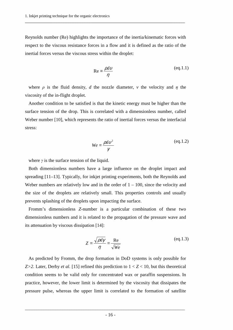
1. Inkjet printing technique for the organic electronics ____________________________________________________________________
____________________________________________________________________ - 16 -
Reynolds number (Re) highlights the importance of the inertia/kinematic forces with
respect to the viscous resistance forces in a flow and it is defined as the ratio of the
inertial forces versus the viscous stress within the droplet:
ηυρd=Re
(eq.1.1)
where ρ is the fluid density, d the nozzle diameter, v the velocity and η the
viscosity of the in-flight droplet.
Another condition to be satisfied is that the kinetic energy must be higher than the
surface tension of the drop. This is correlated with a dimensionless number, called
Weber number [10], which represents the ratio of inertial forces versus the interfacial
stress:
γυρ 2d
We = (eq.1.2)
where γ is the surface tension of the liquid.
Both dimensionless numbers have a large influence on the droplet impact and
spreading [11–13]. Typically, for inkjet printing experiments, both the Reynolds and
Weber numbers are relatively low and in the order of 1 – 100, since the velocity and
the size of the droplets are relatively small. This properties controls and usually
prevents splashing of the droplets upon impacting the surface.
Fromm’s dimensionless Z-number is a particular combination of these two
dimensionless numbers and it is related to the propagation of the pressure wave and
its attenuation by viscous dissipation [14]:
We
dZ
Re==η
γρ
(eq.1.3)
As predicted by Fromm, the drop formation in DoD systems is only possible for
Z>2. Later, Derby et al. [15] refined this prediction to 1 < Z < 10, but this theoretical
condition seems to be valid only for concentrated wax or paraffin suspensions. In
practice, however, the lower limit is determined by the viscosity that dissipates the
pressure pulse, whereas the upper limit is correlated to the formation of satellite

1. Inkjet printing technique for the organic electronics ____________________________________________________________________
____________________________________________________________________ - 17 -
droplets [16]. It is important to classify satellites and satellite-drops. Satellite-drops
are undesired drops generated besides the main drop. In a DOD inkjet printer,
satellite-drops are usually generated when the kinetic energy is too high, so the
ejected liquid column breaks up into more than one drop. In some cases satellite-
drops have the same trajectory as the main drop and may collapse with it if their
velocity is higher than the speed of the main drop. On the contrary, the trajectory of
satellites is not well controlled.
1.4 Ink form1.4 Ink form1.4 Ink form1.4 Ink form ulationulationulationulation
A crucial element for the inkjet printing technology is the ink formulation. The first
and foremost consideration is the compatibility of the fluid with the materials of the
printhead component parts. If the fluid chemically reacts with the elements of the
printhead, the use of the pipette, where only the glass capillary goes in contact with
the ink, is needed.
Moreover, specifically for DOD piezoelectric inkjet technique, the chemico-
physical properties of the fluid that can be ejected by this printing system have very
narrow variability ranges. This depends on the usually quite weak mechanical force
generated by the piezoelectric crystal deformation on the fluid. As a result, the
typical fluid must has sufficiently low viscosity to allow the ejection. By assuming
that all the used fluids exhibit Newtonian properties, the viscosity µ is simply
described as:
•=γ
τµ (eq.1.4)
where τ is the shear stress, that is the required force per unit area to produce the
fluid flow, and •γ is the shear rate, that is the differential velocity of the fluid flow.
For the Microdrop printhead, the ideal fluid viscosity range is 0.5-40 cP. If the
fluid viscosity exceeds this values, the fluid could not be ejected by the piezo
actuation. On the other hand, if the fluid viscosity is too low, the fluid can be idle in
or drip from the nozzle resulting, in this last case, in poor jetting quality with the

1. Inkjet printing technique for the organic electronics ____________________________________________________________________
____________________________________________________________________ - 18 -
presence of filaments or satellites. The ink viscosity is usually adjustable by
modifying the solvent or the material concentration in the fluid.
Although low viscous fluid are desirable for jetting purposes, the high viscosity
guarantee the reduced droplet spreading when the fluid lands on the substrate. The
control of this parameter is critical since the droplet condition strongly influences the
film uniformity. The viscosity range for the printhead employed in this thesis work is
around 20-70 mN/m.
Another important factor in the viability of ink ejection is the size of the particles
in the fluid. Usually, particle diameter smaller than 1 µm in diameter is the right
dimension desirable for eject nanodispersion when using DOD piezoelectric inkjet
printhead. Moreover, the time-stability of the suspension is also a crucial parameter
for the printability of the fluid because the particles in suspension should not
agglomerate for all the time of the printing process.
In addition to the viscosity and time-stability properties, the surface tension is
another important fluid characteristic that must be considered. In general, high
surface tensions don’t allow the fluid separation in forming single drops. On the
other hands, high surface tensions prevent the droplet spread on the substrate so
promoting a spherical shape of the dried printed droplet.
On the contrary, if the surface tension is too low, it is difficult to generate stable
droplets and the fluid element emerging from the needle could show long continuous
tails along the flight path. Moreover, from the wetting perspective, is undesirable to
have very low surface tension because of the wider spreading on the target substrate
that makes difficult the realization of a well defined structure.
Therefore, a good ejecting quality is usually characterised by:
• no wetting of nozzle plate during ejection,
• compatibility with the printhead and the delivery system,
• small ejecting drop volume variation among the generated droplets,
• uniform droplet velocity from droplet to droplet,
• absence of satellite droplets,
• straight droplet trajectory along the nozzle/substrate direction,
• long term ejecting stability, including during the on/off cycles.

1. Inkjet printing technique for the organic electronics ____________________________________________________________________
____________________________________________________________________ - 19 -
The optimization of the drop quality is performed through a vision unit consisting
of a stroboscopic system focused on the nozzle plate allowing the observation of
drops in flight at different phases of generation. Some examples of images from
stroboscopic camera showing various ejecting quality conditions are shown in Figure
1.11.
(a) (b) (c) Figure 1.11 Drop images of a stable condition (a), formation of filament (b) and
formation of satellite droplet (c).
1.5 Ink1.5 Ink1.5 Ink1.5 Ink----substrate system substrate system substrate system substrate system
The non-contact nature of inkjet deposition makes it a very versatile process being
applicable to a wide range of substrates. The interaction between the deposited fluid
and the substrate surface is a crucial factor to optimize the deposition process.
Another critical aspect of the inkjet printing technique for the quality of the printed
material is related to drop drying process which is basically controlled by the so-
known “coffee-stain” effect. During the process of solvent evaporation, a capillary
flow takes place inside the sessile drop from its centre towards the edges, where the
evaporation rate is higher, replenishing the evaporation losses. As consequence, at
the end of the drying process the material results largely localized at the rim of the
printed droplet. Possible approaches to reduce the ‘coffee-stain’ effect are based on
the use of surface treatments (O2, CF4, silane, etc.) and mixtures of solvents with
different boiling points and surface tensions (“Marangoni effect”) in order to modify
the surface energy of the substrate and the surface tension of the liquid, respectively.
In the following sections, more details on the wetting properties of the substrates and
on the coffee-stain and Marangoni effects are provided.

1. Inkjet printing technique for the organic electronics ____________________________________________________________________
____________________________________________________________________ - 20 -
1.5.1 W etting of the substrate1.5.1 W etting of the substrate1.5.1 W etting of the substrate1.5.1 W etting of the substrate
In the printing processes, the main ruling factor in the spreading of the fluid droplet
on the substrate is the surface tension (γ) of components. In general, the molecules in
a fluid are subjected to the attraction of the surrounding molecules. Inside the fluid,
the resultant of all the attraction forces is zero, while on the surface these forces are
directed inwards. This effect of “compression” represents the tendency of every
system to reach the minimum energy state. The increased surface of a liquid
corresponds to an increased energy and, in this case, the equilibrium is reached when
the liquid assume the minimum possible size (spherical shape).
The surface tension is defined as the energy to increase the surface area of a unit.
Therefore, it quantifies the disruption of intermolecular bonds that occurs when a
surface is created and its unit of measurement is energy for unit of area.
The wetting, which is the ability of a liquid to maintain contact with a solid
surface, is determined not only by the liquid surface tension, but even by the surface
energy of the solid and by the balance between adhesive (between molecules in the
liquid and solid) and cohesive forces (between the molecules in the liquid) at the
interface (interfacial tension). Greater adhesive force induces lower interfacial
tension.
In the fluid-substrate interaction, it is more useful to treat the surface tensions as a
system which consists of liquid, solid and vapour interfaces. This approach takes into
account that, when a droplet forms on a surface, three interface tensions generate at
the solid-vapour interface )( svγ , solid-liquid interface )( slγ and liquid-vapour
interface )( lvγ . The base of this concept is schematically illustrated in Figure 1.12.
Figure 1.12 Schema of droplet wetting on a solid surface.
γlv
γsv γsl ϑ
1. Inkjet printing technique for the organic electronics ____________________________________________________________________
____________________________________________________________________ - 21 -
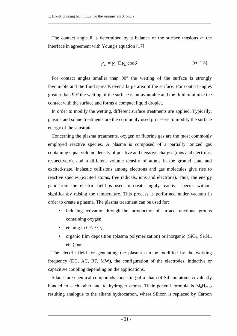
The contact angle θ is determined by a balance of the surface tensions at the
interface in agreement with Young's equation [17]:
θγγγ coslvslsv += (eq.1.5)
For contact angles smaller than 90° the wetting of the surface is strongly
favourable and the fluid spreads over a large area of the surface. For contact angles
greater than 90° the wetting of the surface is unfavourable and the fluid minimize the
contact with the surface and forms a compact liquid droplet.
In order to modify the wetting, different surface treatments are applied. Typically,
plasma and silane treatments are the commonly used processes to modify the surface
energy of the substrate.
Concerning the plasma treatments, oxygen or fluorine gas are the most commonly
employed reactive species. A plasma is composed of a partially ionized gas
containing equal volume density of positive and negative charges (ions and electrons,
respectively), and a different volume density of atoms in the ground state and
excited-state. Inelastic collisions among electrons and gas molecules give rise to
reactive species (excited atoms, free radicals, ions and electrons). Thus, the energy
gain from the electric field is used to create highly reactive species without
significantly raising the temperature. This process is performed under vacuum in
order to create a plasma. The plasma treatment can be used for:
• inducing activation through the introduction of surface functional groups
containing oxygen,
• etching in CF4 / O2,
• organic film deposition (plasma polymerization) or inorganic (SiO2, Si3N4,
etc.) one.
The electric field for generating the plasma can be modified by the working
frequency (DC, AC, RF, MW), the configuration of the electrodes, inductive or
capacitive coupling depending on the applications.
Silanes are chemical compounds consisting of a chain of Silicon atoms covalently
bonded to each other and to hydrogen atoms. Their general formula is SinH2n+2
resulting analogue to the alkane hydrocarbon, where Silicon is replaced by Carbon

1. Inkjet printing technique for the organic electronics ____________________________________________________________________
____________________________________________________________________ - 22 -
atoms. The silane treatment makes a surface hydrophobic by means of its organic
substitution.
1111 .5.2 “Coffee.5.2 “Coffee.5.2 “Coffee.5.2 “Coffee----ring” effectring” effectring” effectring” effect
One of the crucial feature of the printing process is correlated to the droplet drying
process that basically induces a final printed droplet which is characterized by the
presence of high ridges at drop edge. This effect, called “coffee-stain effect”, was
first explained by Deegan et al. in 1997 [18]. This phenomenon describes the
propensity of the solute to flow out towards the droplet edge through a capillary flow
during drying. This occurs owing to the maximum of the evaporation rate and to the
drop pinning at the three-phase contact line [18–21].
During the evaporation of solvents incorporated in a printed droplet, while solvent
molecules evaporating at the center of the droplet are readily reabsorbed, solvent
molecules from the edge can easily escape without any reabsorbing process. This
phenomenon results in a larger evaporation rate around the edge. Such a fast
evaporation at the contact line induces an outward diffusive flow to compensate for
the liquid removed by evaporation and, in turn, transports the suspending solute to
the edge region [22,23].
This effect is represented in figure 1.13.
Figure 1.13 Illustration of “coffee-stain” effect. Evaporation rate (represented by
upward arrows) is highest at the edges of a printed droplet resulting in an accumulation of the solute at the periphery at the end of the drying process.
For this reason, the coffee-stain effect causes a poor uniform distribution of the
printed material which, in general, degrades the final device working.

1. Inkjet printing technique for the organic electronics ____________________________________________________________________
____________________________________________________________________ - 23 -
1.5.3 M arangoni effect1.5.3 M arangoni effect1.5.3 M arangoni effect1.5.3 M arangoni effect
A possible strategy to reduce the “coffee-stain” effect is based on the employment
of mixtures of solvents with different boiling points and surface tensions. By mixing
appropriately two solvents with different chemico-physical properties (surface
tension, boiling point) along the sessile drop radius a concentration gradient of one
solvent is generated opposite to the concentration gradient of the other solvent. The
concentration gradients induce opposite solute capillary flows along the drop radius
profile producing a distribution of the printed material whose final profile depends
on the volume mixing ratio of the solvents suitably combined with their volatility and
surface tension properties. This happens because the droplet drying process is
controlled by Marangoni effect [24,25] in addition to the “coffee-stain effect”. The
Marangoni flow is related to the temperature gradient of the sessile drop and, hence,
to the different surface tension at the droplet liquid-air interface. While the
Marangoni effect is less dominant than the diffusive flow in a single-solvent system,
the same becomes more significant in the case of dual-solvent system in the
definition of the profile of printed droplet. This behaviour is schematically illustrated
in Figure 1.14.
Figure 1.14 Illustration of “Marangoni effect”. The diffusive flow (“coffee-stain”
effect) is directed from the centre to the edge of the printed droplet. If mixture of high- and low- boiling point solvents is employed an inward Marangoni flow can be generate, inducing a balance of material at the centre of the dried droplet.
The physical process responsible of the Marangoni effect is the following. Since
the solvent evaporation requires the consumption of latent heat and the thermal
conduction path is longer at the top centre of the sessile droplet, the surface
temperature is lower at the central region. Since the surface tension is a function of
the temperature, the presence of a gradient of the surface tension along a fluid-fluid
interface induces a Marangoni flow from regions with low surface tension (the film

1. Inkjet printing technique for the organic electronics ____________________________________________________________________
____________________________________________________________________ - 24 -
edges) to regions with high surface tension (the film centre) [24]. In general, in a
single-solvent system, the temperature-gradient-driven Marangoni flow is less
important in the evaporating droplet than the convective flow. Conversely, when
using a mixture of low- and high boiling-point solvents (dual-solvent system), the
solvent composition at the contact line will shift towards more to higher-boiling-
point solvent than that in the bulk due to the fast evaporation of the low-boiling-point
solvent at the edge, creating a compositional-gradient-driven Marangoni flow
[9,26,27]. If the high-boiling-point solvent has a higher surface tension than that of
the low-boiling-point solvent, an outward Marangoni flow is induced from the centre
to the edge. In the opposite case, where the high-boiling-point solvent has a lower
surface tension than that of the low-boiling-point solvent, an inward flow is induced.
Therefore, in a dual-solvent system the Marangoni flow can balance the convective
flow assuming a significant role in defining the shape of the printed droplet. In order
to realize a uniform layer with a reduced “coffee-stain” effect, both the direction and
magnitude of each flow should be well-designed, so an inward flow can be induced
or, in the same way, an outward flow can be suppressed.
1.6 O rganic el1 .6 O rganic el1 .6 O rganic el1 .6 O rganic electronicsectronicsectronicsectronics
Organic electronics is a branch of electronics dealing with carbon-based materials
which are able to carry electric charges. These compounds can be in form of
polymers (macro-molecules) or oligomers (small molecules).
The discovery in 1977 of Shirakawa, MacDiarmid and Heeger on the significant
electrical conduction of doped polymer materials, such as polyacetylene or
polyaniline, exhibited a, promoted a general interest in the study of these materials
[28,29].
Nowadays, organic electronics includes organic conductors, semiconductors,
dielectrics and light emitters. In general, since organic materials are lighter, more
flexible and less expensive than inorganic ones, their use in electronics is making
possible the introduction of new applications. In particular, one of the most
interesting properties of organic materials resides in their solubility in a wide variety

1. Inkjet printing technique for the organic electronics ____________________________________________________________________
____________________________________________________________________ - 25 -
of solvents, making them printable by low-temperature and low-cost techniques. This
specific feature is opening the way to the realization of a broad range of products and
represents a considerable boost to the development of the organic (“plastic”)
electronic technology based on the employment of innovative industrial techniques
like inkjet printing.
In the last decades, most organic materials showing electrical conduction have been
classified as semiconductors. In particular, semiconducting polymers have increased
their potential application in low-cost electronic circuits which can be fabricated on
any substrate type, also having with flexibility and/or transparency properties [30].
Semiconductor polymers were applied as active elements in a broad variety of
devices including light-emitting diodes, solar cells, sensors, and field-effect
transistors (FETs) [31].
Recent researches are focusing also on the possibility to dope polymers with
conductive metal nanoparticles, in order to noticeably increase their basic
conductivity up to values comparable to those of conventional inorganic metals. This
possibility enhances the perspective to fabricate, highly-performing fully-organic
electronic devices in the next future.
In the following, after an introduction to the basic mechanisms which rule the
charge transport phenomena in organic semiconductors, some specific technological
applications, relying on the employment of these materials and which are the subject
of the experimental work reported in this thesis, will be discussed.
1.6.1 Charge transport in organic sem iconductors 1.6.1 Charge transport in organic sem iconductors 1.6.1 Charge transport in organic sem iconductors 1.6.1 Charge transport in organic sem iconductors
According to the band theory of solids, there are three categories of the materials:
conductors, semiconductors and insulators.
The continuum distribution of the energy levels in a solid material is called energy
band. The highest energy band that contains electrons is called the ‘valence band’.
The lowest band in which there are unoccupied states is called ‘conduction band’.
The energy gap between these two bands is called ‘band gap’(Eg) [32].

1. Inkjet printing technique for the organic electronics ____________________________________________________________________
____________________________________________________________________ - 26 -
In insulators, the electrons in the valence band are separated by a large gap (Eg
>2eV) from the conduction band. In conductors like metals, instead, the valence band
overlaps the conduction band and electrons can easily move in response to an
external electrical field due to the presence of accessible energy states. In
semiconductors, there is a small gap (Eg ~1-2 eV) between the valence and
conduction bands, in such a way that thermal or other energy excitations can bridge
the gap (Figure 1.15). Furthermore, in presence of such a small gap, the presence of
low percentages of a doping material can drastically increase the conductivity.
Ene
rgy
ofe
lect
ron
Valence band
Conduction band
Band gap
Valence band
Conduction band
Band gap
Valence band
Conduction band
Insulator Semiconductor Conductor
Ene
rgy
ofe
lect
ron
Valence band
Conduction band
Band gap
Valence band
Conduction band
Band gap
Valence band
Conduction band
Insulator Semiconductor Conductor
Figure 1.15 Schematic representation of Energy bands for insulators,
semiconductors and conductors.
Organic semiconductors, being based on Carbon chemistry, present fundamental
differences with the inorganic ones.
The electronic ground state of carbon (atomic number = 6) is 1s2 2s2 2p2 as
schematically reported in Figure 1.16.
Figure 1.16 Electronic structure of carbon in its ground state.
1. Inkjet printing technique for the organic electronics ____________________________________________________________________
____________________________________________________________________ - 27 -
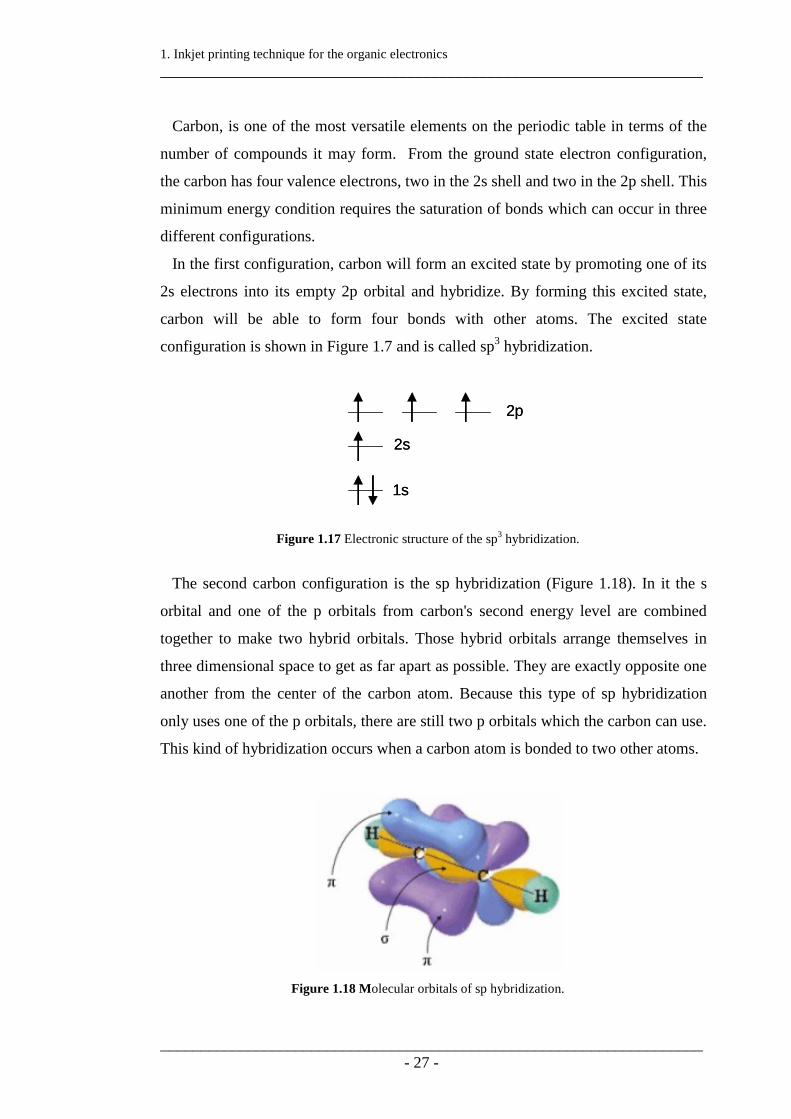
Carbon, is one of the most versatile elements on the periodic table in terms of the
number of compounds it may form. From the ground state electron configuration,
the carbon has four valence electrons, two in the 2s shell and two in the 2p shell. This
minimum energy condition requires the saturation of bonds which can occur in three
different configurations.
In the first configuration, carbon will form an excited state by promoting one of its
2s electrons into its empty 2p orbital and hybridize. By forming this excited state,
carbon will be able to form four bonds with other atoms. The excited state
configuration is shown in Figure 1.7 and is called sp3 hybridization.
1s
2s
2p
1s
2s
2p
Figure 1.17 Electronic structure of the sp3 hybridization.
The second carbon configuration is the sp hybridization (Figure 1.18). In it the s
orbital and one of the p orbitals from carbon's second energy level are combined
together to make two hybrid orbitals. Those hybrid orbitals arrange themselves in
three dimensional space to get as far apart as possible. They are exactly opposite one
another from the center of the carbon atom. Because this type of sp hybridization
only uses one of the p orbitals, there are still two p orbitals which the carbon can use.
This kind of hybridization occurs when a carbon atom is bonded to two other atoms.
Figure 1.18 Molecular orbitals of sp hybridization.

1. Inkjet printing technique for the organic electronics ____________________________________________________________________
____________________________________________________________________ - 28 -
The last configuration is the sp2 hybridization, where three of the valence electrons
form the so-called sp2-hybridized orbitals, which are at an angle of 120° with each
other and stay on the plane (xy). The fourth electron, instead, resides in a so-called pz
orbital which is orthogonal to the xy plane (Figure 1.19a).
(a) (b)
Figure 1.19 (a) sp2-hybridized orbital of a carbon atom; (b) molecular orbitals of
two double bonded carbon atom forming π bonds and σ bonds.
Two of the sp2-hybridized orbitals form σ-type single bonds with two adjacent
atoms. The remaining sp2 hybridized orbital and the pz orbital form a σ bond and a π-
bond with another carbon atom. (Figure 1.19b). Hence, systems of interacting pz
orbitals are called ‘π-conjugated’ systems and characterize the semiconductor
polymer structure. The sp2 configuration is associated with a highly localized
electron density in the plane of the molecule which is the backbone of the conduction
mechanism in the organic semiconductor. The overlap of pz electrons provide
conjugated polymers with desirable electronic properties allowing the transport of
charges.
There are two major classes of organic semiconductors: low molecular weight
materials and polymers. An important difference between the two classes of
materials lies in the way how they are processed to form thin films. Whereas the
small molecules are usually deposited from the gas phase by sublimation or
evaporation, the conjugated polymers can only be processed from solution like by
spin-coating or printing techniques.
In general, the mechanisms ruling the charge transport in organic semiconductors
are basically different from those operating in the conventional inorganic materials.

1. Inkjet printing technique for the organic electronics ____________________________________________________________________
____________________________________________________________________ - 29 -
For the small molecules, due to the weak van der Waals bonding, many electronic
properties of these materials, like the energy gap between the highest occupied and
lowest unoccupied molecular orbitals (HOMO and LUMO) are determined by the
structure of an isolated molecule [33–35]. The weak intermolecular overlap of
electronic orbitals results in narrow electronic bands (a typical bandwidth, Eg ~ 0.1
eV, is one order of magnitude smaller than the Silicon one), a low mobility of
carriers and strong electron-lattice coupling. Moreover, this weak intermolecular
bonding gives consequences also in mechanical and thermodynamic properties
inducing a reduced hardness and a lower melting point. Furthermore, in the polymer
case the charge transport is somewhat different since the morphology of polymer
chains can lead to improved mechanical properties. Nevertheless, the electronic
interaction between adjacent chains is usually also quite weak in this class of
materials.
Depending on the degree of order, the charge carrier transport mechanism in
organic semiconductors can fall between two extreme cases: band or hopping
transport [36].
Band transport is typically observed in molecular crystals (small molecules) at not
too high temperatures. However, since electronic delocalization is weak the
bandwidth is small as compared to inorganic semiconductors (typically few eV at
room temperature). Therefore, room temperature mobilities in molecular crystals
reach values in the range 1 - 10 cm2/Vs. As a typical feature of band transport the
temperature dependence follows a power law behaviour:
nT −∝µ with n= 1…3 (eq. 1.6)
upon going to lower temperature. However, in presence of traps significant
deviations from such a behaviour are observed.
In the case of polymeric materials, the transport is characterized by hopping
mechanism where the charge carriers, free to move along a polymer, are responsible
of the conduction of charge in the polymer films. On the other hand, the disorder in
the film together with polymer defects should however stop or reduce the
conductivity, if it wasn’t for the assistance from phonons (lattice vibration). This

1. Inkjet printing technique for the organic electronics ____________________________________________________________________
____________________________________________________________________ - 30 -
phonon-assisted conduction is described by Mott’s Variable Range Hopping Theory
(VRH) [37,38]. Here interchain conduction is carried out by processes where a
charge can ‘jump’ (tunnel) to a nearby site where its energy can be higher, thanks to
the help of phonons. The charge can then ‘jump’ on further to another chain or travel
along the present polymer chain. Phonons thus enable charges to travel from one side
of a polymer film to the other and at higher temperatures, the more phonons are
available to provide electrons with the extra energy, and, hence higher conductivity
and mobility are achieved increasing in temperature [39]. The mobilities are much
lower then in the single crystal case (around 10–3 cm2/Vs) and are correlated to the
temperature and the applied filed (F) as follows:
kT
F
kT
E
eeTFβ
µ∆
−∝),(
(eq. 1.7)
The solubility of the conjugated materials allows the development of organic inks
which can be processed with different printing methods like inkjet, screen, offset and
gravure printing. In particular, the organic materials differ from conventional
electronics in terms of structure, operation and functionality, which influence device,
circuit design and optimization.
1.7 O rganic electronic applications1.7 O rganic electronic applications1.7 O rganic electronic applications1.7 O rganic electronic applications
Currently, the printing technologies and, specifically, the inkjet printing technique
are very attractive for several applications of organic electronics. Studying some
organic devices fabricated by means IJP allows to understand how the control of the
working parameters of this innovative deposition method can differently affect the
performances of the devices themselves. The present thesis focuses on the following
inkjet printed organic devices: VOC sensors, optical components, OFET and OPV.

1. Inkjet printing technique for the organic electronics ____________________________________________________________________
____________________________________________________________________ - 31 -
1.1.1.1.7.17.17.17.1 Conductive polym er m aterials for sensing Conductive polym er m aterials for sensing Conductive polym er m aterials for sensing Conductive polym er m aterials for sensing
applicationsapplicationsapplicationsapplications
Chemical sensors are devices sensitive to changes in the environment and are able
to convert the changes into signals, giving a qualitative or a quantitative feedback.
The increased attention to pollution, health and safety have enhanced the need and
desire of monitoring the ambient conditions by means of these devices.
Specifically, for the vapour sensing many types of sensors can be employed [40].
These include metal oxide sensors, optical sensors, electrochemical sensors, acoustic
wave sensors, intrinsically conducting polymer chemiresistors and polymer
composite chemiresistors. In particular, for this last class of sensors the possibility to
mix together two materials having complementary behaviours have attracted much
attention for gas sensing applications.
Polymer composite sensors made from composites of conductive carbon black
nanoparticles dispersed in thermoplastic polymers have been developed and studied
extensively in literature. However, so far, they have been fabricated by using
traditional techniques like dip coating or spin casting [40–42].
The possibility of having stable and well dispersed suspensions allows the
employment of the inkjet printing as innovative technique for the fabrication of
sensor devices. This new typology of deposition method is aimed to industrialize the
final products opening new perspectives in application fields like food, fragrances,
environmental monitoring, medical diagnostics and chemical processing.
1.71.71.71.7 ....2222 O ptical grade polym ers for optical structures O ptical grade polym ers for optical structures O ptical grade polym ers for optical structures O ptical grade polym ers for optical structures
In the field of optical applications, the development of optical grade polymer based
inks allows the use of the inkjet printing technology for manufacturing optical
structures. The patterning capability and the possibility to use a single step process
makes this technique interesting for the realization of microlenses and polymer
microstructuring useful for different optoelectronic applications.

1. Inkjet printing technique for the organic electronics ____________________________________________________________________
____________________________________________________________________ - 32 -
An increasingly used technique is inkjet etching, where solvent or solvent mixture
droplets are deposited on soluble polymer surfaces through an inkjet nozzle [43]. At
the end of the drying process, a concave- or convex-shaped surface topology can be
generated. The shape of the microstructure is basically controlled by the surface
tension properties of the droplet acting at the three-phase contact line. The ability to
fabricate small cavities onto solid surfaces is interesting for the development of
chemical, electrical or optical microdevices. These structures can be used for the
fabrication of micro- and nano-pillars [44], microlenses [45], microholes [46], or for
removing interference effects in an optical cavity [47].
The additive deposition of solutions of optical grade polymers allows the
realization of optical components, such as refractive microlenses, which can be
incorporated in many systems and commercial products. They are used, for example,
for focusing in detector arrays, fibre optics and sensors, for illumination in flat panel
displays, computers and for imaging in photocopiers and lithography [48].
Refractive microlenses are fabricated with different processes like
photolithographic [49,50], electroforming [50], melting process [51] and inkjet
printing process [52–54]. In particular, the inkjet printing technique is suitable for
producing single lenses and large arrays of high optical property refractive
microlenses using a very simple and flexible deposition method.
1.1.1.1.7.37.37.37.3 O rganic sem iconductor for transistor applications O rganic sem iconductor for transistor applications O rganic sem iconductor for transistor applications O rganic sem iconductor for transistor applications
In the field of the organic electronics, the development of organic semiconductors
which are air stable and soluble in common solvents allows the fabrication of organic
field effect transistors (OFETs) by printing techniques.
Organic field-effect transistors (OFETs) are 3-terminal devices in which the charge
carrier density in the channel between source and drain contacts can be controlled by
the applied gate voltage across a thin dielectric (Figure 1.20). In the organic
semiconductor the charge transport takes place mainly at the interface between
organic semiconductor and a gate dielectric with respect to the bulk.

1. Inkjet printing technique for the organic electronics ____________________________________________________________________
____________________________________________________________________ - 33 -
Figure 1.20 Schema of organic field effect transistor.
Recent developments of OFETs are aimed at different applications as organic
displays [55], complementary circuits [56] and all-polymer integrated circuits [57].
In particular, the solution processing of organic materials for OFET applications is
suited for low-cost fabrication, roll to roll deposition and easy patterning of the
electronic structures.
In Figure 1.21 some examples of the most commonly used organic semiconductors
(polymers or small molecules) are reported. For both n-type (electron transporting)
and p-type (hole transporting) semiconductors it is possible to observe the presence
of aromatic rings, corresponding to π-bonds of atoms which are alternately single-
and double-bonded to another one.
(a)
poly(p-phenylene) pentacene
polypyrrole polythiophene
poly(p-phenylene) pentacene
polypyrrole polythiophene (b) Perylene DiimidePerylene Diimide
Figure 1.21 Examples of chemical structure of (a) p-type and (b) n-type conjugated polymer semiconductors.

1. Inkjet printing technique for the organic electronics ____________________________________________________________________
____________________________________________________________________ - 34 -
1.6.5 Polym er blend for sol1.6.5 Polym er blend for sol1.6.5 Polym er blend for sol1.6.5 Polym er blend for solar cell applications ar cell applications ar cell applications ar cell applications
An emerging application field of the organic electronics is represented by the
organic photovoltaic (OPV), a possible answer to the need of clean and renewable
energy.
Despite the expanding use of inorganic semiconductors, the organic
semiconductors enable the fabrication of solar modules with several potential
advantages, including light-weight, flexibility, low-cost manufacturing and
possibility of creating large-area devices. While organic low-molecular-weigh
semiconductors are generally deposited by evaporation process, the conjugated
polymers are usually deposited from solution by using wet processing techniques like
dip-coating, spin-coating, inkjet printing, doctor blading and others. These
techniques represent an interesting way for producing OPV cells because they can be
performed under ambient conditions (temperature and pressure) and scaled up to
large area with minimized loss of material.
At present bulk heterojunction structures, based on blends of polymer donors and
highly soluble fullerene-derivative acceptors, are currently the most efficient
architecture for polymer solar cells.

1. Inkjet printing technique for the organic electronics ____________________________________________________________________
____________________________________________________________________ - 35 -
B ibliographyB ibliographyB ibliographyB ibliography
[1] Hue P. Le, Progress and Trends in Ink-jet Printing Technology, Journal of Imaging Science and Technology. 42 (1998) 42-62.
[2] Eric R . Lee, Microdrop Generation, 2003. [3] J.-U. Park, M. Hardy, S.J. Kang, K. Barton, K. Adair, D. kishore
Mukhopadhyay, et al., High-resolution electrohydrodynamic jet printing, Nat Mater. 6 (2007) 782-789.
[4] P. Calvert, Inkjet Printing for Materials and Devices, Chemistry of Materials. 13 (2001) 3299-3305.
[5] E. Tekin, H. Wijlaars, E. Holder, D.A.M. Egbe, U.S. Schubert, Film thickness dependency of the emission colors of PPE?PPVs in inkjet printed libraries, J. Mater. Chem. 16 (2006) 4294.
[6] T.H.J. van Osch, J. Perelaer, A.W.M. de Laat, U.S. Schubert, Inkjet Printing of Narrow Conductive Tracks on Untreated Polymeric Substrates, Advanced Materials. 20 (2008) 343-345.
[7] A.M.J. van den Berg, A.W.M. de Laat, P.J. Smith, J. Perelaer, U.S. Schubert, Geometric control of inkjet printed features using a gelating polymer, J. Mater. Chem. 17 (2007) 677.
[8] B. Derby, Bioprinting: inkjet printing proteins and hybrid cell-containing materials and structures, J. Mater. Chem. 18 (2008) 5717.
[9] B.-J. de Gans, U.S. Schubert, Inkjet Printing of Well-Defined Polymer Dots and Arrays, Langmuir. 20 (2004) 7789-7793.
[10] G.O. Thomas, The aerodynamic breakup of ligaments, Atomiz Spr. 13 (2003) 117-129.
[11] J. Fukai, Z. Zhao, D. Poulikakos, C.M. Megaridis, O. Miyatake, Modeling of the deformation of a liquid droplet impinging upon a flat surface, Phys. Fluids A. 5 (1993) 2588.
[12] S. Sikalo, M. Marengo, C. Tropea, E.N. Ganic, Analysis of impact of droplets on horizontal surfaces, Experimental Thermal and Fluid Science. 25 (2002) 503-510.
[13] T. Mao, D.C.S. Kuhn, H. Tran, Spread and rebound of liquid droplets upon impact on flat surfaces, AIChE J. 43 (1997) 2169-2179.
[14] Numerical Calculation of the Fluid Dynamics of Drop-on-Demand Jets, (2001).
[15] N. Reis, C. Ainsley, B. Derby, Ink-jet delivery of particle suspensions by piezoelectric droplet ejectors, J. Appl. Phys. 97 (2005) 094903.
[16] K.A.M. Seerden, N. Reis, J.R.G. Evans, P.S. Grant, J.W. Halloran, B. Derby, Ink Jet Printing of Wax Based Alumina Suspensions, Journal of the American Ceramic Society. 84 (2001) 2514-2520.
[17] P.-G. de Gennes, F. Brochard-Wyart, D. Quere, Capillarity and Wetting Phenomena: Drops, Bubbles, Pearls, Waves, 1st ed., Springer, 2003.
[18] R.D. Deegan, O. Bakajin, T.F. Dupont, G. Huber, S.R. Nagel, T.A. Witten, Capillary flow as the cause of ring stains from dried liquid drops, Nature. 389 (1997) 827-829.

1. Inkjet printing technique for the organic electronics ____________________________________________________________________
____________________________________________________________________ - 36 -
[19] R.D. Deegan, Stress hysteresis as the cause of persistent holes in particulate suspensions, Phys. Rev. E. 81 (2010) 036319.
[20] R.D. Deegan, O. Bakajin, T.F. Dupont, G. Huber, S.R. Nagel, T.A. Witten, Contact line deposits in an evaporating drop, Phys. Rev. E. 62 (2000) 756.
[21] B.-J. de Gans, S. Hoeppener, U.S. Schubert, Polymer relief microstructures by inkjet etching, J. Mater. Chem. 17 (2007) 3045.
[22] T. Kawase, H. Sirringhaus, R.H. Friend, T. Shimoda, Inkjet Printed Via Hole Interconnections and Resistors for All Polymer Transistor Circuits, Advanced Materials. 13 (2001) 1601-1605.
[23] E. Bonaccurso, H.-J. Butt, B. Hankeln, B. Niesenhaus, K. Graf, Fabrication of microvessels and microlenses from polymers by solvent droplets, Appl. Phys. Lett. 86 (2005) 124101.
[24] H. Hu, R.G. Larson, Marangoni Effect Reverses Coffee-Ring Depositions, The Journal of Physical Chemistry B. 110 (2006) 7090-7094.
[25] S. Jeong, D. Kim, J. Moon, Ink-Jet-Printed Organic−Inorganic Hybrid Dielectrics for Organic Thin-Film Transistors, The Journal of Physical Chemistry C. 112 (2008) 5245-5249.
[26] J. Park, J. Moon, Control of Colloidal Particle Deposit Patterns within Picoliter Droplets Ejected by Ink-Jet Printing, Langmuir. 22 (2006) 3506-3513.
[27] P. Takhistov, H.-C. Chang, Complex Stain Morphologies, Industrial & Engineering Chemistry Research. 41 (2002) 6256-6269.
[28] H. Shirakawa, E.J. Louis, A.G. MacDiarmid, C.K. Chiang, A.J. Heeger, Synthesis of electrically conducting organic polymers: halogen derivatives of polyacetylene, (CH)x, Journal of the Chemical Society, Chemical Communications. (1977) 578.
[29] C.K. Chiang, C.R. Fincher, Y.W. Park, A.J. Heeger, H. Shirakawa, E.J. Louis, et al., Electrical Conductivity in Doped Polyacetylene, Phys. Rev. Lett. 39 (1977) 1098.
[30] R. Farchioni, G. Grosso, Organic Electronic Materials: Conjugated Polymers and Low Molecular Weight Organic Solids, 1st ed., Springer, 2001.
[31] H.S. Nalwa, Handbook of Organic Conductive Molecules and Polymers, Conductive Polymers: Transport, Photophysics and Applications (Handbook of Organic Conductive Molecules & Polymers), 1st ed., Wiley, 1997.
[32] P. Chandrasekhar, Conducting Polymers, Fundamentals and Applications: A Practical Approach, 1st ed., Springer, 1999.
[33] E.A. Silinsh, V. Capek, Organic Molecular Crystals: Interacton Localization, and Transport Phenomena, 1st ed., American Institute of Physics, 1997.
[34] M. Pope, C.E. Swenberg, Electronic Processes in Organic Crystals and Polymers, 2nd ed., Oxford University Press, 1999.
[35] K.-C. Kao, Electrical transport in solids: with particular reference to organic semiconductors, 1st ed., Pergamon Press, Oxford;;New York, 1981.
[36] W. Bruetting, Physics of Organic Semiconductors, 1st ed., Wiley-VCH, 2005.
[37] N.F. Mott, On the transition to metallic conduction in semiconductors, Can. J. Phys. 34 (1956) 1356-1368.
[38] E.M. Conwell, Impurity Band Conduction in Germanium and Silicon, Phys. Rev. 103 (1956) 51.

1. Inkjet printing technique for the organic electronics ____________________________________________________________________
____________________________________________________________________ - 37 -
[39] P.W.M. Blom, M.C.J.M. Vissenberg, Charge transport in poly(p-phenylene vinylene) light-emitting diodes, Materials Science and Engineering: R: Reports. 27 (2000) 53-94.
[40] K.J. Albert, N.S. Lewis, C.L. Schauer, G.A. Sotzing, S.E. Stitzel, T.P. Vaid, et al., Cross-reactive chemical sensor arrays, Chem. Rev. 100 (2000) 2595-2626.
[41] B.J. Doleman, R.D. Sanner, E.J. Severin, R.H. Grubbs, N.S. Lewis, Use of compatible polymer blends to fabricate arrays of carbon black-polymer composite vapor detectors., Analytical Chemistry. 70 (1998) 2560-2564.
[42] M.C. Lonergan, E.J. Severin, B.J. Doleman, S.A. Beaber, R.H. Grubbs, N.S. Lewis, Array-Based Vapor Sensing Using Chemically Sensitive, Carbon Black−Polymer Resistors, Chem. Mater. 8 (2011) 2298-2312.
[43] R. Pericet-Camara, E. Bonaccurso, K. Graf, Microstructuring of Polystyrene Surfaces with Nonsolvent Sessile Droplets, ChemPhysChem. 9 (2008) 1738-1746.
[44] C.H. Liu, J.A. Zapien, Y. Yao, X.M. Meng, C.S. Lee, S.S. Fan, et al., HighDensity, Ordered Ultraviolet Light-Emitting ZnO Nanowire Arrays, Advanced Materials. 15 (2003) 838-841.
[45] S. Karabasheva, S. Baluschev, K. Graf, Microstructures on soluble polymer surfaces via drop deposition of solvent mixtures, Applied Physics Letters. 89 (2006) 031110.
[46] T. Kawase, H. Sirringhaus, R.H. Friend, T. Shimoda, Inkjet Printed Via Hole Interconnections and Resistors for All Polymer Transistor Circuits, Advanced Materials. 13 (2001) 1601-1605.
[47] F. Villani, I.A. Grimaldi, G. Nenna, A.D.G. Del Mauro, F. Loffredo, C. Minarini, Study of the interference effects in an optical cavity for organic light-emitting diode applications, Opt. Lett. 35 (2010) 3333-3335.
[48] N.M. Presby, C.R. Giles, Asymmetric fiber microlenses for efficient coupling to elliptical laser beams, IEEE Photonics Technology Letters. 5 (1993) 184-186.
[49] D. Daly, R.F. Stevens, M.C. Hutley, N. Davies, The manufacture of microlenses by melting photoresist, Measurement Science and Technology. 1 (1990) 759-766.
[50] K.-H. Brenner, M. Kufner, S. Kufner, J. Moisel, A. Moller, S. Sinzinger, et al., Application of three-dimensional micro-optical components formed by lithography, electroforming, and plastic molding, Appl. Opt. 32 (1993) 6464-6469.
[51] Hutley M. C, Optical Techniques for the Generation of Microlens Arrays, (1990).
[52] R. Danzebrink, M.. Aegerter, Deposition of optical microlens arrays by ink-jet processes, Thin Solid Films. 392 (2001) 223-225.
[53] Refractive microlens fabrication by ink-jet process, (S.d.). [54] R. Danzebrink, M.. Aegerter, Deposition of micropatterned coating using an
ink-jet technique, Thin Solid Films. 351 (1999) 115-118. [55] A. Dodabalapur, Z. Bao, A. Makhija, J.G. Laquindanum, V.R. Raju, Y.
Feng, et al., Organic smart pixels, Applied Physics Letters. 73 (1998) 142.

1. Inkjet printing technique for the organic electronics ____________________________________________________________________
____________________________________________________________________ - 38 -
[56] Y.-Y. Lin, A. Dodabalapur, R. Sarpeshkar, Z. Bao, W. Li, K. Baldwin, et al., Organic complementary ring oscillators, Applied Physics Letters. 74 (1999) 2714.
[57] C.J. Drury, C.M.J. Mutsaers, C.M. Hart, M. Matters, D.M. de Leeuw, Low-cost all-polymer integrated circuits, Applied Physics Letters. 73 (1998) 108.

____________________________________________________________________ - 39 -
CHAPTER 2
SENSORS
Chemical sensor research represents a rich field of study utilizing a wide array of
technologies and materials to accomplish the difficult task of converting sensory
information into quantifiable chemical, optical or electrical signals. The need to
extract increasing amounts of sensory information from our environment fuels the
development of sensors that are easier to manufacture, capable of miniaturization,
and more sensitive to vapours that excite greater interest. Recently, polymer
nanocomposites, whose two component materials have synergic or complementary
behaviours, have attracted much attention in different of device applications, such as
gas sensors. The possibility to obtain stable and well dispersed suspensions allows
the employment of inkjet printing technique for the realization of the sensor devices
in a very cheap way. Moreover, this class of vapour-phase sensors has the advantage
of using a non-destructive and non-invasive detection method, suitable for green and
food applications.
The present chapter is focused on the fabrication and related characterization of
chemical sensors by printing a specific polymer nanocomposite based on polystyrene
(PS) polymer and Carbon Black (CB) as conductive filler. A study on the sensing
properties of this material to volatile organic compounds (VOCs) and on the
influence of the printing parameters and the geometrical patterning on the sensing
performances is carried out. Moreover, a study aimed to the optimization of the ink
deposition on different flexible and non-flexible substrates is also performed.

2. Sensors ____________________________________________________________________
____________________________________________________________________ - 40 -
2222 .1.1.1.1 Conductive polym er nanocom posites Conductive polym er nanocom posites Conductive polym er nanocom posites Conductive polym er nanocom posites
In recent years, volatile organic compounds (VOCs) chemical sensors are
increasingly relying on the use of polymer nanocomposites (PNCs) as sensing
materials. Nanosized conductive inorganic fillers dispersed in insulating polymeric
matrices belong to the broader category of the PNCs. The conductivity and
mechanical-stability properties of nanoparticles combined with the simple
processability of polymers, the low cost of both production and materials, the
possibility of easy and cheap manufacture of large area devices and the possibility of
varying the polymer composition and, hence, the properties of the organic materials,
make the resultant hybrid system attractive in a wide range of polymer-based devices
such as light emitting diodes [1-3], photodiodes [4], solar cells [5], magnetic storage
materials [6] and gas sensors [7].
Conductive sensing films from composites of conductive Carbon Black (CB)
nanoparticles dispersed in thermoplastic polymers have been developed and studied
extensively by Lewis [8-11], Ho [12-14] and others [15-18].
2222 .1.1.1.1 .1.1.1.1 Sw elling m echanism Sw elling m echanism Sw elling m echanism Sw elling m echanism
The working mechanism of these sensors is based on the properties of absorption
of the polymer matrix upon exposure to vapour molecules. This mechanism produces
an increase of the polymer matrix volume, also known “swelling process”. The
presence of conductive fillers dispersed in the polymer generates the transduction
mechanism, based on the change of the electrical conductivity. Indeed, an increase of
the polymer volume corresponds to a reduction of the conductive filler volumetric
fraction determining a disruption of the conductive paths and a change in
electrophysical characteristics of the composite [19-28]. Upon organic vapors
exposure this class of sensors undergoes a reversible change in electrical resistance.
The physical mechanism is schematically illustrated in Figure 2.1.

2. Sensors ____________________________________________________________________
____________________________________________________________________ - 41 -
(a) (b)
(c)
Figure 2.1 Analyte detection: (a) the electrical current flows across the conductive film; (b) the absorption of VOCs into the polymer causes the swelling and the breaking of conductive pathways, so increasing the electrical resistance (c) the analyte is removed and the resistance returns to initial value through a reversible process.
2222 .2 G eom etry role in the sensor perform ance.2 G eom etry role in the sensor perform ance.2 G eom etry role in the sensor perform ance.2 G eom etry role in the sensor perform ancessss
Recently, the ink jet printing technology (IJP) was proven to be an useful technique
in the deposition of PNCs films up to now prepared by techniques such as spin-
coating or drop-casting [29-32], spray [33]. The advantages of the IJP over the
aforementioned techniques lie in its potential for printing on both nonflexible and
flexible substrates, the efficient use of materials, the reduced waste products, low
cost of the process, low processing temperature and its patterning capability. As for
this last item, the IJP technology assumes a key role in the feasibility of modifying
the sensitive material geometry in controlled and extremely easy manner in order to
optimize the sensor response. A deep study of the sensor properties, such as
sensitivity, response time and limit of detection, as function of the geometrical
configuration and of the printed layer number is useful for the optimization of the gas
sensor device performances.
2222 .2.1 Sensing film : ink form ulation and characterizations.2.1 Sensing film : ink form ulation and characterizations.2.1 Sensing film : ink form ulation and characterizations.2.1 Sensing film : ink form ulation and characterizations
The sensing material chosen for the thesis activity is a polystyrene (PS)/carbon
black (CB) composite. The atactic polystyrene (Sigma-Aldrich, weight average
molecular mass Mw = 25000) was chosen for its sensing property to different
organic chemical compounds (acetone, ethanol, toluene, benzene, …). The Carbon

2. Sensors ____________________________________________________________________
____________________________________________________________________ - 42 -
Black (CB), used as conductive filler in preparation of composites, was Carbon
Black Pearls 2000 (Cabot Co.). This is a furnace carbon black material with 1500
m2/g specific surface area, 12 nm average particle size and with 150 g/L density. The
PS matrix (80 mg) was dissolved in n-Methyl-2-pyrrolidone (NMP) and the CB
nanoparticles (20 mg) were dispersed in the polymeric solution (0.5 wt. %) by means
of ultrasonic bath for 90 minutes at room temperature. The PS/CB suspension was
finally filtered using a 0.2 µm filter (PTFE) in order to remove bigger agglomerates.
The schematic ink preparation is reported in Figure 2.2.
+
Polymeric solution(Polystyrene + N- Methyl Pyrrolidone)
Conducting Filler (Carbon Black)
=
PS/CB in NMP(0.4 wt.%)
+
Polymeric solution(Polystyrene + N- Methyl Pyrrolidone)
Conducting Filler (Carbon Black)
=
PS/CB in NMP(0.4 wt.%)
Figure 2.2 Ink preparation: the polystyrene was dissolved in NMP and the Carbon Black was dispersed in the polymeric solution.
The employed substrates (5x5 mm2) were made of alumina (Euroacciai S.R.L) with
which interdigitated Au electrodes which were previously e-beam evaporated and
subjected to a standard lift-off photolithographic process. The interdigitated
electrodes are characterized by the following geometrical parameters: the finger
length (Lfinger) is equal to 700 µm, the finger width (Wfinger) is 100 µm, the gap
distance between two adjacent fingers (Igap) is 100 µm and the number of fingers
(Nfinger) is 10. The alumina substrate was chosen for its porous and sliver-shaped
surface promoting a good adhesion of the ink on the substrate so assuring a wide
sensitive surface.
The functional PS/CB ink was characterized throug Dynamic Laser Scattering
(DLS) analysis using a HPPS 3.1 (Malvern Instruments) to determine the average
particle size and size distribution of filler in suspension and the dispersion stability in
the solutions. Therefore, the inks were characterized by DLS at different aging times.
In Figure 2.3 are reported the results of DLS analysis. A typical distribution curve of

2. Sensors ____________________________________________________________________
____________________________________________________________________ - 43 -
the CB particle size in the dispersion presents a peak centered at about 200 nm
(Figure 2.3a) and polydispersity index values (PDI) range between 0.12 and 0.18
(Figure 2.3a). These results confirmed the good quality of dispersion process. These
parameters resulted roughly constant for an observation time of about 2 years
indicating a good time stability for the dispersion (Figure 2.3b). The results of this
analysis, combined with the viscosity (2.42 mPa×s) and surface tension (46 mN/m)
properties of the suspension, indicated that the dispersion can be employed as ink
[34]. Indeed, crucial elements of a dispersion to be dispensed by an inkjet printhead
are both the time-stability and the particle size in suspension, which must be less than
1/100 of the nozzle diameter, to prevent clogging and blockage of the nozzle itself
and the entire capillary. Therefore, these parameters indicate that the prepared PS/CB
suspension can be suitably processed by the inkjet printing system.
Figure 2.3 (a) Distribution curve of the CB particles size for PS/CB dispersion; (b)
nanoparticles average size (square) and PDI (circle) measured in the aging time from 0 to 600 days by DLS analysis.
2222 .2.2 Sensor device assem bly.2.2 Sensor device assem bly.2.2 Sensor device assem bly.2.2 Sensor device assem bly
The processed dispersion was used as ink and printed onto 50 °C heated
electrodes/substrate system. The inkjet equipment employed for the device
realization was already described in Chapter 1. The Microdrop printhead has a 70 µm
opening nozzle corresponding to ~268 pL droplet volume. The driving parameters
are the following: pulse width = 75 µs and a driver voltage = 46V. The sensing
material geometries consist of one or more lines, created by overlapped droplet
sequences (50 % overlap degree, 0.5 Hz drop emission frequency, 0.05 mm/s
printhead speed), differently orientated with respect to the transducer fingers.

2. Sensors ____________________________________________________________________
____________________________________________________________________ - 44 -
The layers were deposited by IJ printing the sensing material in five different
geometries. Each geometry consists of one or more lines parallel or transverse to the
fingers of the interdigitated electrodes; the fifth geometry is a cross. Moreover, two
different configurations were fabricated with three- and penta-overlapped layers for
each pattern with the aim of investigating the thickness effect on the sensor
performances. The optical micrographs (Polyvar MET Reichert-Jung) of the samples
with different geometries are shown in Figure 2.4. The gold electrodes are
represented by the most bright part of the images.
Before investigating the sensor device working, the morphological analysis of the
printed layers was carried out in order to get useful information on the sensor
behaviour. In Figure 2.5 the SEM (SEM, LEO 1530) image of a three-layer sample is
shown as comparison with the simple substrate used as reference. The printed PS/CB
distribution on the alumina substrate (Figure 2.5a) is characterized by wide
uncovered areas and by a clearly porous structure of the printed ink which permit a
good interaction between the gas and the polymer nanocomposite material. The SEM
image of the substrate surface is reported as reference in Figure 2.5b. This analysis
showed that multiple layers are necessary to cover the porous structure of the
substrate and to obtain a conductive continuous film.
(a) (b)
(c) (d) (e)
Figure 2.4 Optical micrographs of printed devices with different geometries: (a) transverse single-line, (b) transverse double-lines, (c) parallel single-line, (d) parallel three-lines, (e) cross.
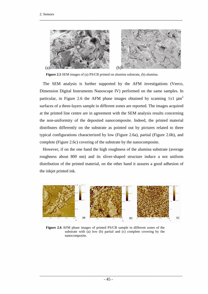
2. Sensors ____________________________________________________________________
____________________________________________________________________ - 45 -
(a) (b)
Figure 2.5 SEM images of (a) PS/CB printed on alumina substrate, (b) alumina.
The SEM analysis is further supported by the AFM investigations (Veeco,
Dimension Digital Instruments Nanoscope IV) performed on the same samples. In
particular, in Figure 2.6 the AFM phase images obtained by scanning 1x1 µm2
surfaces of a three-layers sample in different zones are reported. The images acquired
at the printed line centre are in agreement with the SEM analysis results concerning
the non-uniformity of the deposited nanocomposite. Indeed, the printed material
distributes differently on the substrate as pointed out by pictures related to three
typical configurations characterized by low (Figure 2.6a), partial (Figure 2.6b), and
complete (Figure 2.6c) covering of the substrate by the nanocomposite.
However, if on the one hand the high roughness of the alumina substrate (average
roughness about 800 nm) and its sliver-shaped structure induce a not uniform
distribution of the printed material, on the other hand it assures a good adhesion of
the inkjet printed ink.
Figure 2.6 AFM phase images of printed PS/CB sample in different zones of the
substrate with (a) low (b) partial and (c) complete covering by the nanocomposite.

2. Sensors ____________________________________________________________________
____________________________________________________________________ - 46 -
2222 .2.3 E lectrical characterization under analyte vapours.2.3 E lectrical characterization under analyte vapours.2.3 E lectrical characterization under analyte vapours.2.3 E lectrical characterization under analyte vapours
A volt-amperometric technique, at constant bias, was employed for sensor dc
electrical characterization. The sensor response was measured upon exposure to
acetone vapours at different concentrations (600, 1250, 2500, and 5000 ppm) in a
Gas Sensor Characterization System (Kenosistec equipment) that allows to monitor
and control pressure, flow rate, actual gas composition, humidity and environment
temperature. The test chamber at ENEA Portici is showed in Figure 2.7.
Figure 2.7 Gas sensor characterization system for electrical analysis under different
organic vapours.
In such a system the device was placed in a stainless steel test chamber placed in a
thermostatic box at controlled temperature (20 °C) and humidity (30%). A constant
flow rate (500 cm3/min) of the gas carrier (nitrogen) crosses the test chamber. The
carrier can be properly humidified through a water bubbler placed in a thermostatic
bath.
In this environment, characterized by controlled temperature and humidity, the
resistance value of the device in its equilibrium state is firstly measured (baseline);
after that, an intentional disruption of the equilibrium state is produced by
introducing a controlled amount of VOC analyte and by mixing it with the gas carrier
for a time step of 3000 s. To validate and monitor the gas mixture, a thermo Antaris
IGS FTIR analyzer is placed at the gas output in order to measure the chemical
compounds concentration in the test chamber with a resolution of ppm.

2. Sensors ____________________________________________________________________
____________________________________________________________________ - 47 -
Hardware and software, implemented on a work station, allow to control and
record environmental parameters, device bias and output signal, making possible to
perform customizable automated tests on devices for the measurement of sensor
parameters such as sensitivity, response time, noise and limit-of-detection (LoD). In
detail, the sensitivity is expressed in terms of the relative differential response
O
O
R
RR −, where OR is the sensor baseline resistance and R is the sensor resistance
upon exposure to solvent vapours. Moreover, the LoD is defined as the analyte
concentration at which a sensor response corresponds to signal-to-noise ratio (S/N)
equal to 3, in according with the conventional definition by IUPAC [32]. The
response time is defined as the time required for the signal to change from 10 % to
90 %.
The electrical sensor response upon exposure to 600, 1250, 2500, and 5000 ppm of
acetone vapours for three-layers and penta-layers devices are reported in Figure 2.8a
and Figure 2.8b, respectively.
(a) (b)
Figure 2.8 (a) Three-layers and (b) penta-layers sensors electrical responses to
acetone vapours.
The parameters that characterized the three-layers sensor performances are
summarized in
Table 2.1, while the ones for the penta-layers are reported in Table 2.2.

2. Sensors ____________________________________________________________________
____________________________________________________________________ - 48 -
Morphology Resistance [KOhm]
Sensitivity [1/ppm]
Limit-of-Detection [ppm]
Noise Response time [s]
Cross 13.3 1.34*E-6 100 0.94*E-4 100 2 lines transverse 38.5 1.83*E-6 150 0.88*E-4 100 Single line transverse 57.6 1.07*E-6 180 1.2*E-4 100 3 lines parallel 95.7 0.81*E-6 560 2.1*E-4 100 Single line parallel 1000 4.43*E-7 560 3.5*E-4 100
Table 2.1 Resistance, sensitivity, limit of detection and response time of 3-layers sensors to
acetone vapours.
Morphology Resistance
[KOhm] Sensitivity [1/ppm]
Limit-of-Detection [ppm]
Noise Response time [s]
2 lines transverse 8,6 2,43*E-6 60 1.0*E-4 >3000 Single line transverse 8,9 2.18*E-6 75 1.3*E-4 >3000 3 lines parallel 50 1.74*E-6 200 1.4*E-4 >3000 Single line parallel 175 1.05*E-6 300 1.5*E-4 >3000
Table 2.2 Resistance, sensitivity, limit of detection and response time of 5-layers sensors to
acetone vapours.
The results indicated that, for whatever investigated geometry, the three-layers
sensors were all faster than penta-layers devices. Indeed, the response time for the
three-layers devices was equal to 100 s, one order of magnitude lower than the one of
penta-layers devices (>3000 s). In this last case, the real time response value couldn’t
be estimated because the sensor response didn’t reach the saturation level in the
investigated exposure time for each analyte concentration. This behaviour can be
attributed to the physisorption mechanism of the gas molecules in the polymer
matrix. At the nanoscale, the solvent molecules can very quickly enter in the free
volumes of the amorphous phase and modify the CB/matrix interaction by
adsorption. The inability of the penta-layer sensors to achieve the saturation
condition can be attributed to the reduced surface/volume ratios with respect to the
three-layer configuration because of the higher material quantity. Moreover, for all
the investigated samples, when the analyte is removed, the resistance drop back to
the initial values, revealing the complete desorption of the solvent molecules from
the polymer matrix and full reversibility of the devices.
The correlation between the base resistance and sensitivity is confirmed in the case
of penta-layers devices (see Table 2.2), which are characterized by a lower base
resistance than the three-layers ones. Indeed, a higher number of layers of sensing
2. Sensors ____________________________________________________________________
____________________________________________________________________ - 49 -
material increases the amount of the sensing material inducing the highest relative
differential responses.
However, generally the dynamic responses of sensors with different geometries are
strongly influenced by the base resistance R0. In fact, by comparing the different
geometries of the three-layers configuration, the performances of the devices with
‘transverse’ geometry are better than the ones of the ‘parallel’ geometry devices in
terms of the sensitivity, noise and the limit-of-detection (LoD) (see
Table 2.1). Both the increase of VOC sensitivity and the decrease of LoD and noise
indicate an improvement of the performances corresponding to a lower base
resistance of the devices. This behaviour can be easily explained by comparing the
single-line geometries. Indeed, since the equivalent circuit of the ‘transverse’
geometry is composed by multiple resistors placed in parallel, the device
transduction effect in this geometry is enhanced with respect to the ‘parallel’
geometry. The multiple-lines geometries are ruled by the same mechanism, even if in
a more complex manner.
The different geometries were realized taking into account the transducer geometry
and the minimum dimension of the printed sensing material line width. In particular,
the cross geometry was projected in order to increase the sensing surface with respect
to the ‘transverse’ single-line. The dynamic response of the cross device effectively
showed an improvement with respect to the ‘transverse’ single-line in terms of both
sensitivity and LoD, but in a less significant manner if compared with the
‘transverse’ two-lines geometry. This behaviour is easily explained since the printed
material along the ‘parallel’ direction and not comprised between two contiguous
fingers weakly influences the electrical response (second order effects). This
statement is confirmed by the dynamic responses of the ‘parallel’ geometries (single-
and three-lines) which showed the worst performances.
In Figure 2.9 the calibration curves of both the three-layers configurations (Figure
2.9a) and penta-layers (Figure 2.9b) are reported. The reported data for all the
geometries are interpolated by linear fits. The calibration curves analysis allows to
determine both the sensitivity (the angular coefficient of the calibration curve) and
LoD parameters. The results indicated that the electrical response varies linearly as

2. Sensors ____________________________________________________________________
____________________________________________________________________ - 50 -
the analyte concentration increases for all the manufactured chemical sensors in all
the investigated concentration range (600, 1250, 2500, and 5000 ppm).
(a) (b) Figure 2.9 Calibration curves of the (a) three-layers and (b) penta-layers sensors for
all the different geometries.
2222 .3 F lexible substrates for sensor device fabrication.3 F lexible substrates for sensor device fabrication.3 F lexible substrates for sensor device fabrication.3 F lexible substrates for sensor device fabrication
The study reported in the previous paragraph indicates that the geometry with
printed line ‘transverse’ to interdigitated contacts gives the best sensor performances
in terms of sensitivity and limit of detection. Moreover, the three-lines configuration
is preferred thanks to its faster response with respect to the penta-layers. These
sensors were fabricated on alumina substrates which can be replaced with flexible
ones. The feasibility of processing material solutions on flexible substrates replacing
the rigid ones is a key role of the emerging inkjet printing technique.
The interaction ink/substrate system has fundamental role in the device
performances since it induces different morphologies of the printed material. In this
thesis activity, glass, PET (polyethylene terephthalate) and glossy paper (Epson)
were employed as substrates for the inkjet printing deposition. The effect of the
substrate morphology on the printed film quality and, hence, on the device
performances upon exposure to acetone and ethanol vapours were investigated.
Furthermore, a comparison with the alumina substrate was performed.
The sensible material (PS/CB) was printed with the optimized geometry on
alumina substrate such as with lines ‘transverse’ to the interdigitated contacts in the
configuration of overlapped 3-layers. It was necessary to optimize the deposition for
PET and glass substrates by means of chemico-physical surface treatments such as

2. Sensors ____________________________________________________________________
____________________________________________________________________ - 51 -
oxygen plasma (O2) or carbon tetrafluoromethane plasma (CF4). These treatments
allow to modify the wetting of the ink/substrate system and the surface roughness of
the substrate in order to obtain continuous printed lines.
2222 .3.1 Printing optim ization by surface treat.3.1 Printing optim ization by surface treat.3.1 Printing optim ization by surface treat.3.1 Printing optim ization by surface treatm entsm entsm entsm ents
Overlapped drops of nanocomposite based ink were IJ-printed on patterned PET,
glass and glossy paper substrates. For glass and PET substrates the spreading of the
sensing material resulted not optimized for the presence of empty regions in the
printed material in the case of PET substrate (Figure 2.10a) and for a not uniform and
not controllable deposition in the case of glass substrate (Figure 2.10b). For the
glossy paper substrate, thanks to its surface characteristic, the ink deposition was
optimized without the application of any chemico-physical treatment (Figure 2.10c).
For PET and glass substrates, surface treatments were required to modify the
wetting of the ink/substrate system. Oxygen plasma (O2) and fluorine plasma (CF4)
treatments were employed to modify the surface energy of the substrates. A contact
angle instrument (OCA20, Dataphysics) was used in order to evaluate the
hydrophobicity and hydrofilicity of the surfaces by extiming the disperse and polar
components of the surface energy. The measurements were made by dispensing on
the substrates drops of water, as polar solvent, and dichloromethane, as apolar
solvent, and by fitting the results with the Owen, Wendt, Rabel and Kaelble
(OWRK) method [35].
(a) (b)
UntreatedUntreated
(c)
Figure 2.10 Optical images of the printed line on PET (a), glass (b) and glossy paper (c) substrates.

2. Sensors ____________________________________________________________________
____________________________________________________________________ - 52 -
This measurement gives indication on the wetting of the ink/substrate system
considering the measured value of the surface tension of the PS/CB equal to γ = 56
mN/m.
In Figure 2.11 are reported the 1 µL water droplets dispensed with the contact
angle instrument on untreated and CF4- and O2-plasma treated PET and glass
substrates.
O2PlasmaO
2PlasmaCF
4PlasmaCF
4Plasma
Glass
PET
Untreated
Figure 2.11 Water droplets on untreated and CF4 and O2 plasma treated glass and
PET substrates
For PET substrate, CF4 plasma treatment makes the substrate more hydrophobic
(contact angle greater than 90°) while O2 treatment makes it more hydrophilic
(contact angle lower than 90°). Concerning the glass substrate, both CF4- and O2-
plasmas make the substrate hydrophilic. Therefore, in the case of polymer substrate,
the CF4 plasma treatment results in the formation of a thin fluorinated layer making
the substrate surface hydrophobic, while for the glass substrate this kind of treatment
performs a double action, cleaning and etching, increasing the substrate surface
energy making it more hydrophilic [36]. The analysis of the results of the contact
angle measurements are summarized in Table 2.3.
Morphology Substrates Rq [nm] θθθθpol [°] θθθθdisp [°] Surface Energy
[mN/m] Glass 0.6 28.5 14.6 43.1 Untreated PET 2.4 5.6 38.5 44.1 Glass 0.7 24.7 35.8 60.5 CF4 plasma PET 4.3 0.4 13.5 13.9 Glass 0.7 32.2 44.9 77.1 O2 plasma PET 2.5 30.7 50.0 80.7
Table 2.3 Summary of the substrate characteristics before and after plasma treatments: means
roughness (Rq), polar component (θpol) and disperse component (θdisp) of the surface energy.

2. Sensors ____________________________________________________________________
____________________________________________________________________ - 53 -
In detail, for glass substrate the plasma treatments don’t modify the surface
roughness but considerably increase the surface energy. Taking into account that a
good wetting condition is obtained when the substrate surface energy is grater than
the ink surface tension, the action of O2 plasma on the glass surface consists in
increasing its surface energy up tu 77 mN/m, consequently inducing the splashing of
the ink on the target substrate. On the contrary, the CF4 plasma allows to reach an
intermediate surface energy value (SE = 60.5 mN/m) corresponds to an optimal
deposition condition.
For PET substrate the CF4 plasma treatment involves an increase of the surface
roughness and a more significant decrease of the polar component of the surface
energy than the apolar one, so making the substrate more hydrophobic. Despite the
surface energy is lower than the surface tension, the higher roughness guarantees the
formation of a continuous line by pinning the printed droplets. On the contrary, after
the O2 treatment, the higher surface energy of the substrate doesn’t allow the
formation of a continuous line and produce a not uniform condition with a splashing
and not controllable deposition.
2222 .3.2 Sensor .3 .2 Sensor .3 .2 Sensor .3 .2 Sensor device fabricationdevice fabricationdevice fabricationdevice fabrication
As showed in the previous paragraph the surface treatments can modify the
roughness and the surface energy of the substrates. In particular, the CF4 plasma
optimizes the ink deposition for both glass and PET substrates. In Figure 2.12 are
reported the printed line transverse to interdigitated contacts with a continuous and a
well defined profile, as expected.
(a) (b) Figure 2.12 Optical images of the printed line on PET substrate (a) and glass
substrate (b) after CF4 plasma treatment.
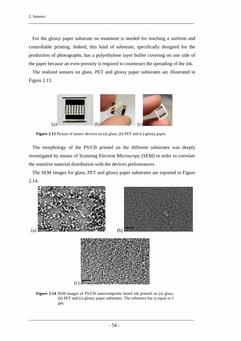
2. Sensors ____________________________________________________________________
____________________________________________________________________ - 54 -
For the glossy paper substrate no treatment is needed for reaching a uniform and
controllable printing. Indeed, this kind of substrate, specifically designed for the
production of photographs, has a polyethylene layer buffer covering on one side of
the paper because an even porosity is required to counteract the spreading of the ink.
The realized sensors on glass, PET and glossy paper substrates are illustrated in
Figure 2.13.
(a) (b) (c) Figure 2.13 Picture of sensor devices on (a) glass, (b) PET and (c) glossy paper.
The morphology of the PS/CB printed on the different substrates was deeply
investigated by means of Scanning Electron Microscopy (SEM) in order to correlate
the sensitive material distribution with the devices performances.
The SEM images for glass, PET and glossy paper substrates are reported in Figure
2.14.
(a) (b)
(c)
Figure 2.14 SEM images of PS/CB nanocomposite based ink printed on (a) glass, (b) PET and (c) glossy paper substrates. The reference bar is equal to 2 µm.

2. Sensors ____________________________________________________________________
____________________________________________________________________ - 55 -
The SEM analysis shows the presence of percolative paths of the conductive filler
in the polymer matrix for all the substrates. Moreover, for PET and, in particular, for
glossy paper (Figure 2.14b,c) the CB distribution is more uniform than the glass
substrate (Figure 2.14a), where empty regions alternated to a more concentrated
areas are present. The morphology of the PS/CB printed on all the substrates is
completely different from that observed on the alumina one (Figure 2.5). The last
one, which is the most commonly employed in literature for its sensor performances,
have a characteristic sliver morphology that increases the adhesion and the surface
active area of the sensitive material. The different morphology observed on glass,
PET and glossy paper can affect the adsorption of the organic vapours and, hence,
the sensing performance of the devices.
2222 .3.3 E lectrical characterization to acetone vapours.3.3 E lectrical characterization to acetone vapours.3.3 E lectrical characterization to acetone vapours.3.3 E lectrical characterization to acetone vapours
The devices electrical responses of the three layers devices to acetone vapors are
shown in Figure 2.15 (a),(b),(c) for glass, PET and glossy paper substrates,
respectively.
(a) (b)
(c)
Figure 2.15 Electrical responses of 3-layers sensors on glass (a), PET (b) and glossy paper (c) in presence of acetone vapours.

2. Sensors ____________________________________________________________________
____________________________________________________________________ - 56 -
The parameters that characterize the sensor performances, such as base resistance,
sensitivity, limit of detection (LoD) and response time, are summarized in Table 2.4
for each substrate.
Substrate Resistance
[KOhm] Sensitivity [1/ppm]
Limit-of-Detection [ppm]
Noise Response time [s]
Glass 300 3.13 e-6 350 5.2 e-4 200 PET 135 3.67 e-6 50 1.1 e-4 >3000 Glossy paper 8,8 8.50 e-7 30 1.0 e-4 100
Table 2.4 Base resistance, sensitivity, limit of detection and response time of 3-layers sensors printed on glass, PET and glossy paper substrates to acetone vapours.
As showed in the dynamic response, the devices obtained on glass and PET
substrates don’t reach the saturation condition for all the analyte concentration. This
effect could be due to the presence of printed edge where the large amount of
sensitive material makes the adsorption of the solvent more difficult. On the
contrary, the device on glossy paper showed the best sensor performances in terms of
both response time and limit of detection, with respect to the other substrates and
also alumina one thanks to the better ink-substrate interaction that indices to a better
distribution of the CB filler in the polymer matrix printed on this substrate.
Figure 2.16 Calibration curves of the three-layers sensors exposed to acetone
vapours fabricated on glass (square), PET (circle) and glossy paper (triangle).
In Figure 2.16 the calibration curves for the sensors fabricated on glass, PET and
glossy paper are reported. The data reported in order to compare all the devices are
interpolated by linear fits. For each substrate, the electrical response varies linearly
as the analyte concentration increases from 600 to 5000 ppm.

2. Sensors ____________________________________________________________________
____________________________________________________________________ - 57 -
2222 .3.4 E lectrical characterization to ethanol vapours.3.4 E lectrical characterization to ethanol vapours.3.4 E lectrical characterization to ethanol vapours.3.4 E lectrical characterization to ethanol vapours
All the fabricated sensors on the different substrates were characterized also under
ethanol vapours. The exposition to this vapours was made in order to study the
selectivity of the sensing material to different analytes.
The electrical responses to 600, 1250, 2500 and 5000 ppm of ethanol for the sensor
realized on glass, PET and glossy paper substrates are reported in Figure 2.17.
(a) (b)
(c)
Figure 2.17 Electrical responses of 3-layers sensors on glass (a), PET (b) and glossy paper (c) to ethanol vapours.
In Table 2.5 the parameters that characterize the three sensors under ethanol
vapours are summarized.
Substrate Resistance
[KOhm] Sensitivity [1/ppm]
Limit-of-Detection [ppm]
Noise Response time [s]
Glass 300 8,6 e-7 400 3.1 e-4 500 PET 135 7,8 e-7 150 1.9 e-4 >3000 Glossy paper 8,8 6,0 e-7 100 1.0 e-4 100
Table 2.5 Base resistance, sensitivity, limit of detection and response time of 3-layers sensors
printed on glass, PET and glossy paper substrates to ethanol vapours.
As highlighted in the electrical responses, both glass and PET substrates don’t
reach the saturation condition neither at lower concentrations. On the contrary, the

2. Sensors ____________________________________________________________________
____________________________________________________________________ - 58 -
sensor realized on glossy paper shows the best limit-of-detection and response time
characteristics and reaches the saturation condition up to 2500 ppm in about 100 s.
In Figure 2.18, the calibration curves of the sensor devices in presence of ethanol
vapours are reported. Even if the device on glass substrate shows the best sensitivity,
the sensor on glossy paper has the lowest LoD, noise and response time thanks to the
morphology induced by the suitable ink/substrate interaction which is confirmed by a
very low base resistance.
In any case, the electrical response of all the sensors to ethanol vapours are worst
of about one order of magnitude with respect to acetone. The worst performances
could be explained considering that the ethanol is more polar than the acetone one.
Because the polystyrene molecule, for its intrinsic chemical structure, has higher
affinity to non-polar molecules, its sensitivity to ethanol vapour is lower than to
acetone.
Figura 2.18 Calibration curves of the three-layers sensors on glass, PET and glossy
paper exposed to ethanol vapours.
2222 .4 Sum m ary.4 Sum m ary.4 Sum m ary.4 Sum m ary
The second chapter of the thesis activity involved the manufacture and
characterization of nanocomposite based chemical sensors on different, flexible and
not flexible, substrates and investigated how their performances are related to printed
film quality induced by the ink-substrate system interactions. The sensing material
was deposited by means of ink-jet printing technique on alumina, glass, PET and
glossy paper substrates. The sensing material morphology was characterized by
means of SEM and AFM analysis. The sensor responses were measured upon
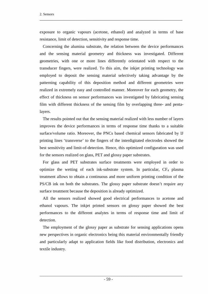
2. Sensors ____________________________________________________________________
____________________________________________________________________ - 59 -
exposure to organic vapours (acetone, ethanol) and analyzed in terms of base
resistance, limit of detection, sensitivity and response time.
Concerning the alumina substrate, the relation between the device performances
and the sensing material geometry and thickness was investigated. Different
geometries, with one or more lines differently orientated with respect to the
transducer fingers, were realized. To this aim, the inkjet printing technology was
employed to deposit the sensing material selectively taking advantage by the
patterning capability of this deposition method and different geometries were
realized in extremely easy and controlled manner. Moreover for each geometry, the
effect of thickness on sensor performances was investigated by fabricating sensing
film with different thickness of the sensing film by overlapping three- and penta-
layers.
The results pointed out that the sensing material realized with less number of layers
improves the device performances in terms of response time thanks to a suitable
surface/volume ratio. Moreover, the PNCs based chemical sensors fabricated by IJ
printing lines ‘transverse’ to the fingers of the interdigitated electrodes showed the
best sensitivity and limit-of-detection. Hence, this optimized configuration was used
for the sensors realized on glass, PET and glossy paper substrates.
For glass and PET substrates surface treatments were employed in order to
optimize the wetting of each ink-substrate system. In particular, CF4 plasma
treatment allows to obtain a continuous and more uniform printing condition of the
PS/CB ink on both the substrates. The glossy paper substrate doesn’t require any
surface treatment because the deposition is already optimized.
All the sensors realized showed good electrical performances to acetone and
ethanol vapours. The inkjet printed sensors on glossy paper showed the best
performances to the different analytes in terms of response time and limit of
detection.
The employment of the glossy paper as substrate for sensing applications opens
new perspectives in organic electronics being this material environmentally friendly
and particularly adapt to application fields like food distribution, electronics and
textile industry.

2. Sensors ____________________________________________________________________
____________________________________________________________________ - 60 -
B ibliographyB ibliographyB ibliographyB ibliography
[1] M.V.M. Rao, Y.K. Su, T.-S. Huang, M.-L. Tu, S.-S. Wu, C.-Y. Huang,
Enhanced Performance of Polymer Light Emitting Devices Using Zinc Oxide Nanoparticle with Poly(vinylcarbazole), J. Electrochem. Soc. 157 (2010) H832-H836.
[2] V.L. Colvin, M.C. Schlamp, A.P. Alivisatos, Light-emitting diodes made from cadmium selenide nanocrystals and a semiconducting polymer, Nature. 370 (1994) 354-357.
[3] M.C. Schlamp, X. Peng, A.P. Alivisatos, Improved efficiencies in light emitting diodes made with CdSe(CdS) core/shell type nanocrystals and a semiconducting polymer, J. Appl. Phys. 82 (1997) 5837.
[4] T. Nyberg, Macromolecular nanoelectronics, Current Applied Physics. 2 (2002) 27-31.
[5] Z. Liu, D. He, Y. Wang, H. Wu, J. Wang, Solution-processable functionalized graphene in donor/acceptor-type organic photovoltaic cells, Solar Energy Materials and Solar Cells. 94 (2010) 1196-1200.
[6] S. Douadi-Masrouki, B. Frka-Petesic, M. Save, B. Charleux, V. Cabuil, O. Sandre, Incorporation of magnetic nanoparticles into lamellar polystyrene-b-poly(n-butyl methacrylate) diblock copolymer films: Influence of the chain end-groups on nanostructuration, Polymer. 51 (2010) 4673-4685.
[7] Y.S. Kim, Fabrication of carbon black-polymer composite sensors using a position-selective and thickness-controlled electrospray method, Sensors and Actuators B: Chemical. 147 (2010) 137-144.
[8] K.J. Albert, N.S. Lewis, C.L. Schauer, G.A. Sotzing, S.E. Stitzel, T.P. Vaid, et al., Cross-Reactive Chemical Sensor Arrays, Chemical Reviews. 100 (2000) 2595-2626.
[9] R.D.S. B J Doleman, Use of compatible polymer blends to fabricate arrays of carbon black-polymer composite vapor detectors., Analytical chemistry. 70 (1998) 2560-4.
[10] M.C. Lonergan, E.J. Severin, B.J. Doleman, S.A. Beaber, R.H. Grubbs, N.S. Lewis, Array-Based Vapor Sensing Using Chemically Sensitive, Carbon Black−Polymer Resistors, Chemistry of Materials. 8 (1996) 2298-2312.
[11] M.E. Koscho, R.H. Grubbs, N.S. Lewis, Properties of Vapor Detector Arrays Formed through Plasticization of Carbon Black−Organic Polymer Composites, Analytical Chemistry. 74 (2002) 1307-1315.
[12] C.K. Ho, E.R. Lindgren, K.S. Rawlinson, L.K. McGrath, J.L. Wright, Development of a Surface Acoustic Wave Sensor for In-Situ Monitoring of Volatile Organic Compounds, Sensors. 3 (2003) 236-247.
[13] C.K. Ho, R.C. Hughes, In-Situ Chemiresistor Sensor Package for Real-Time Detection of Volatile Organic Compounds in Soil and Groundwater, Sensors. 2 (2002) 23-34.
[14] H. Lei, W.G. Pitt, L.K. McGrath, C.K. Ho, Modeling carbon black/polymer composite sensors, Sensors and Actuators B: Chemical. 125 (2007) 396-407.

2. Sensors ____________________________________________________________________
____________________________________________________________________ - 61 -
[15] W.P. Carey, B.R. Kowalski, Chemical piezoelectric sensor and sensor array characterization, Analytical Chemistry. 58 (1986) 3077-3084.
[16] F. Zee, J.W. Judy, Micromachined polymer-based chemical gas sensor array, Sensors and Actuators B: Chemical. 72 (2001) 120-128.
[17] M.P. Eastman, R.C. Hughes, G. Yelton, A.J. Ricco, S.V. Patel, M.W. Jenkins, Application of the Solubility Parameter Concept to the Design of Chemiresistor Arrays, J. Electrochem. Soc. 146 (1999) 3907-3913.
[18] A. Marquez, J. Uribe, R. Cruz, Conductivity variation induced by solvent swelling of an elastomer–carbon black–graphite composite, Journal of Applied Polymer Science. 66 (1997) 2221-2232.
[19] D. Goustouridis, K. Manoli, S. Chatzandroulis, M. Sanopoulou, I. Raptis, Characterization of polymer layers for silicon micromachined bilayer chemical sensors using white light interferometry, Sensors and Actuators B: Chemical. 111-112 (2005) 549-554.
[20] S. Chatzandroulis, D. Goustouridis, I. Raptis, Characterization of polymer films for use in bimorph chemical sensors, J. Phys.: Conf. Ser. 10 (2005) 297-300.
[21] A. Convertino, G. Leo, M. Tamborra, C. Sciancalepore, M. Striccoli, M.L. Curri, et al., TiO2 colloidal nanocrystals functionalization of PMMA: A tailoring of optical properties and chemical adsorption, Sensors and Actuators B: Chemical. 126 (2007) 138-143.
[22] A. Carrillo, I.R. Martín-Domínguez, A. Márquez-Lucero, Modeling and experimental testing of the effect of solvent absorption on the electric properties of styrene butadiene rubber/carbon black chemical sensors, Sensors and Actuators B: Chemical. 113 (2006) 477-486.
[23] A. De Girolamo Del Mauro, A.I. Grimaldi, V. La Ferrara, E. Massera, M.L. Miglietta, T. Polichetti, et al., A Simple Optical Model for the Swelling Evaluation in Polymer Nanocomposites, Journal of Sensors. 2009 (2009) 1-6.
[24] S. Shang, L. Li, X. Yang, Y. Wei, Polymethylmethacrylate-carbon nanotubes composites prepared by microemulsion polymerization for gas sensor, Composites Science and Technology. 69 (2009) 1156-1159.
[25] J. Lu, B.J. Park, B. Kumar, M. Castro, H.J. Choi, J.-F. Feller, Polyaniline nanoparticle–carbon nanotube hybrid network vapour sensors with switchable chemo-electrical polarity, Nanotechnology. 21 (2010) 255501.
[26] F. Cakar, M.R. Moroglu, H. Cankurtaran, F. Karaman, Conducting poly(ether imide)-graphite composite for some solvent vapors sensing application, Sensors and Actuators B: Chemical. 145 (2010) 126-132.
[27] M.C. Lonergan, E.J. Severin, B.J. Doleman, S.A. Beaber, R.H. Grubbs, N.S. Lewis, Array-Based Vapor Sensing Using Chemically Sensitive, Carbon Black−Polymer Resistors, Chemistry of Materials. 8 (1996) 2298-2312.
[28] Briglin S.M., Freund M.S., Tokumaru P., Lewis N.S., Exploitation of spatiotemporal information and geometric optimization of signal/noise performance using arrays of carbon black-polymer composite vapor detectors, Sensors and Actuators B: Chemical. 82 (2002) 54-74.
[29] B. Ballarin, A. Fraleoni-Morgera, D. Frascaro, S. Marazzita, C. Piana, L. Setti, Thermal inkjet microdeposition of PEDOT:PSS on ITO-coated glass and characterization of the obtained film, Synthetic Metals. 146 (2004) 201-205.

2. Sensors ____________________________________________________________________
____________________________________________________________________ - 62 -
[30] Y. Yoshioka, G.E. Jabbour, Desktop inkjet printer as a tool to print conducting polymers, Synthetic Metals. 156 (2006) 779-783.
[31] F. Loffredo, G. Burrasca, L. Quercia, D.D. Sala, Gas Sensor Devices Obtained by Ink-jet Printing of Polyaniline Suspensions, Macromolecular Symposia. 247 (2007) 357-363.
[32] F. Loffredo, A.D.G.D. Mauro, G. Burrasca, V. La Ferrara, L. Quercia, E. Massera, et al., Ink-jet printing technique in polymer/carbon black sensing device fabrication, Sensors and Actuators B: Chemical. 143 (2009) 421-429.
[33] J. Lu, B. Kumar, M. Castro, J.-F. Feller, Vapour sensing with conductive polymer nanocomposites (CPC): Polycarbonate-carbon nanotubes transducers with hierarchical structure processed by spray layer by layer, Sensors and Actuators B: Chemical. 140 (2009) 451-460.
[34] P. Atkins, Atkins’ Physical Chemistry, 7th ed., Oxford Higher Education, 2001.
[35] D.K. Owens, R.C. Wendt, Estimation of the surface free energy of polymers, Journal of Applied Polymer Science. 13 (1969) 1741-1747.
[36] C. Sele, T. von Werne, R. Friend, H. Sirringhaus, Lithography-Free, Self-Aligned Inkjet Printing with Sub-Hundred-Nanometer Resolution, Advanced Materials. 17 (2005) 997-1001.

____________________________________________________________________ - 63 -
CHAPTER 3
OPTICAL STRUCTURES
Photonics is one of the six key enabling technologies (Kets) identified by the
European Commission as essential to realize the great challenges of the future in a
competitive way. Within the world of photonics, the Solid State Lighting (SSL) has
held great interest especially thanks to the many applications arising from the
possible use of the inkjet printing technology.
In recent years, the inkjet printing technique is attracting more and more interest in
the framework of optical structures fabrication, overcoming the drawbacks of the
traditional techniques which usually require multiple complex processing steps
making the fabrication costly.
Inkjet printing technique is generally used as tool for positioning small quantities
of a liquid material on a target substrate. For this reason it can be used as a direct
method for the fabrication of high-quality and high-precision optical microstructures
(i.e. microlenses, microholes, polymer texturing…) with the great advantage to be
extremely versatile in definition of the patterns of microstructures and in the
employed polymer materials.
An interesting application of the inkjet printing is the so called ‘inkjet etching’
(IJE) that consists in depositing drops of solvent or solvent mixtures onto a soluble
polymer layer. This technique allows to structure the polymer film with the profile
that can have concave or convex shape by varying the mixing ratio of the solvents.

3. Optical structures ____________________________________________________________________
____________________________________________________________________ - 64 -
In this chapter, the structuring of some polymeric layers (polyimide and
polystyrene) by solvents (N-Methyl-2-pyrrolidone (NMP), toluene (TOL)) and
solvent mixture (TOL:NMP) at different volume mixing ratios were studied and the
effect of the printing parameters on the microstructure profile was investigated.
Moreover, optical microstructures were also fabricated by inkjet additive
deposition of Poly(methyl methacrylate) (PMMA) solutions dissolved in different
solvents (NMP, TOL) and the effects of the printing parameters on the shape and the
geometry and, hence, on the optical characteristics of the microstructures were
studied.

3. Optical structures ____________________________________________________________________
____________________________________________________________________ - 65 -
3.13.13.13.1 Introduction to polym er m icrostructuringIntroduction to polym er m icrostructuringIntroduction to polym er m icrostructuringIntroduction to polym er m icrostructuring
The structuring of materials is employed for different applications such as
realization of biochips and micropatterned cell arrays [1,2], patterning for building
‘bank’ structures [3], fabrication of microlens array [4,5] and texturing of surfaces
[6] in order to improve the efficiency of OLED (organic light-emitting diode) and
photovoltaic devices [7,8]. Several methods are proposed for polymer
microstructuring and normally they use costly and multiple process steps. One of the
most innovative method is the inkjet etching (IJE), an application of the inkjet
printing (IJP) technology. The IJE, a single-process technique, consists in depositing
pure solvent or mixture of solvents onto a soluble polymer layer, creating
microstructures whose shape is function of the mixing ratio.
In general, when a single-solvent drop is printed, a crater-shaped microstructure is
created on the polymer surface. Indeed, when the solvent drop hits the polymer layer,
the polymer is locally dissolved, carried from the sessile drop centre to the edges and
deposited there. This phenomenon occurs owing to the maximum of the evaporation
rate and to the drop pinning at the three-phase contact line [9-13]. The motion of this
convective flow inside the drop and directed towards its rim leads to a not uniform
solute deposition with an accumulation of material at the edges, at the end of the
drying process [14,15]. This phenomenon is known as “coffee-stain effect” [9,13,16].
Additionally, the redistribution of the polymer dissolved by a single-solvent drop
also depends on the contribution of the Marangoni flow but in less significant way
than the diffusive flow. The Marangoni flow is related to the temperature gradient of
the sessile drop, and, hence, to the different surface tensions at the droplet liquid-air
interface, and generates a solute motion from droplet rim to the centre [17]. The
contribution of the Marangoni flow becomes more important in the definition of the
final profile of the polymer when a dual-solvent system formed by solvents with
different evaporation rates is employed. By using a mixture of high- and low-boiling
point solvents, a concentration gradient of one solvent opposite to the concentration
gradient of the other solvent is generated along the sessile drop radius. In this case,
the solvent volatility and the surface tension properties combined with the mixing

3. Optical structures ____________________________________________________________________
____________________________________________________________________ - 66 -
ratio allow to control the capillary flows inside the droplet and to vary the
microstructure shape from concave to convex.
Moreover, by changing the number of the drops of the pure solvent or the solvent
mixture, the morphological properties and the geometry of the structures also change
[13].
3.2 Inkjet etching of polym er surface3.2 Inkjet etching of polym er surface3.2 Inkjet etching of polym er surface3.2 Inkjet etching of polym er surface
The polymer substrates employed for the IJE process were polyimide (PI) and
poly(styrene) (PS), chosen for their good optical transmission properties in the
spectral range and thermo-mechanical properties.
Commercial glass substrates purchased from Schott were cleaned by sonication
with deionised water, acetone and isopropanol, dried with nitrogen and finally placed
in oven at 130 °C for 1 hour.
After cleaning process, the PI and PS polymeric films were deposited on glass
substrates by means of a Brewer Science Model 100 spin coater. The PI film, 1 µm
thick, was spun at 5000 rpm for 30 s employing a 2 mL volume of the commercial
solution (PI 2556) purchased from HD Microsystems. The PS sample was deposited
by employing 2 mL of a solution of the commercial PS (Aldrich, average Mw ~
350,000) dissolved in chlorobenzene at 90 °C for 30 min with a concentration of 15
% (w/w). The PS film thickness was 5.3 µm by spin-coating at 500 rpm for 20 s.
All the polymeric samples were placed on a hot plate at 100 °C for 15 min in order
to completely remove the solvent.
N-methyl-2-pyrrolidon (NMP) and Toluene (TOL) were chosen as solvents
because they dissolve the investigated polymers and have good chemico-physical
properties for the inkjet printing process. Drops of NMP and TOL were inkjet printed
onto the PI and PS layers, respectively. Moreover, the structuring of the PS film was
performed also by printing TOL:NMP mixtures at different mixing ratios (1:1, 1.5:1,
1.8:1, 2:1, 2.3:1, 3:1). NMP was chosen for the PI structuring because the precursor
monomers of the purchased PI are dissolved in it. As for the PS structuring, the
choice of using TOL as single-solvent system and TOL and NMP as mixture

3. Optical structures ____________________________________________________________________
____________________________________________________________________ - 67 -
components arises from the fact that both dissolve the PS layer and are miscible
together. Furthermore, these solvents have different volatility and surface tension
properties (TOL: Tb = 110.6 °C, γ = 28.53 mN/m; NMP: Tb = 202 °C, γ = 40 mN/m)
and their evaporation rates are suitable for inkjet printing processing.
The droplet depositions were performed by means of the inkjet equipment already
described in the chapter 1 of this thesis, employing printhead with 50 or 70 µm
opening nozzle corresponding to 90 or 180 pL droplet volume.
For the PS layer, sequences of TOL and TOL:NMP droplets were printed by means
of the 50 µm opening nozzle printhead at the 6.7 Hz drop emission frequency and 1
mm/s printhead speed with a spacing between the droplets of 160 µm so creating a
square array of microstructures on the polymer layer.
Similarly, for the PI layer, sequences of NMP droplets were printed by means of
the 70 µm opening nozzle printhead at the 5 Hz drop emission frequency and 2 mm/s
printhead speed with a spacing between the droplets of 400 µm.
After the structuring, only PI samples were thermally treated with a curing process
at 200 °C for 30 min in air and at 300 °C for 1 hour in nitrogen atmosphere.
3.2.1 3.2.1 3.2.1 3.2.1 PI structured by N M PPI structured by N M PPI structured by N M PPI structured by N M P
The inkjet etching process using a single solvent system was employed onto PI
film. By inkjet printing NMP drops on the polymer layer, crater-shaped
microstructures form on polymer surface at the end of the solvent evaporation. The
typical 2-dimensional profile of the microstructure has a central spherically shaped
cavity and two lateral humps as shown in Figure 3.1.
In Figure 3.1 the structural parameters that characterize the microcrater profile are
also reported: Wc is the width at cavity bottom (Wc = 0 in the case represented in
Figure 3.1), Wo the internal diameter, We the diameter at the cavity top, Wtot the
external diameter, Hec the total depth of the cavity, and, finally, He and Hc are the
edge height and the cavity depth with reference to the unstructured external polymer
surface, respectively. These geometrical parameters are pointed in order to
quantitatively monitor as the microstructure profile changes by varying the printing
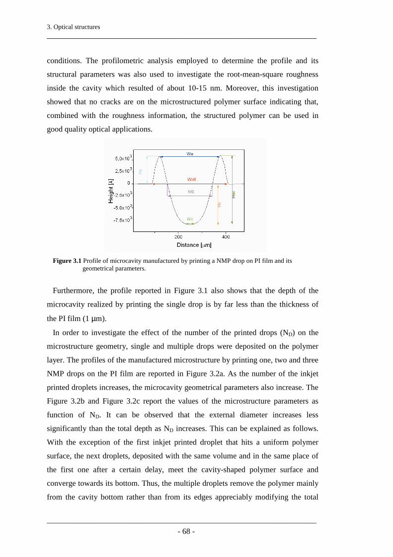
3. Optical structures ____________________________________________________________________
____________________________________________________________________ - 68 -
conditions. The profilometric analysis employed to determine the profile and its
structural parameters was also used to investigate the root-mean-square roughness
inside the cavity which resulted of about 10-15 nm. Moreover, this investigation
showed that no cracks are on the microstructured polymer surface indicating that,
combined with the roughness information, the structured polymer can be used in
good quality optical applications.
Figure 3.1 Profile of microcavity manufactured by printing a NMP drop on PI film and its
geometrical parameters.
Furthermore, the profile reported in Figure 3.1 also shows that the depth of the
microcavity realized by printing the single drop is by far less than the thickness of
the PI film (1 µm).
In order to investigate the effect of the number of the printed drops (ND) on the
microstructure geometry, single and multiple drops were deposited on the polymer
layer. The profiles of the manufactured microstructure by printing one, two and three
NMP drops on the PI film are reported in Figure 3.2a. As the number of the inkjet
printed droplets increases, the microcavity geometrical parameters also increase. The
Figure 3.2b and Figure 3.2c report the values of the microstructure parameters as
function of ND. It can be observed that the external diameter increases less
significantly than the total depth as ND increases. This can be explained as follows.
With the exception of the first inkjet printed droplet that hits a uniform polymer
surface, the next droplets, deposited with the same volume and in the same place of
the first one after a certain delay, meet the cavity-shaped polymer surface and
converge towards its bottom. Thus, the multiple droplets remove the polymer mainly
from the cavity bottom rather than from its edges appreciably modifying the total
3. Optical structures ____________________________________________________________________
____________________________________________________________________ - 69 -
depth (47 % percentage variation) and leaving the external diameter almost
invariable (9 % percentage variation).
Figure 3.2 (a) Profiles of the PI microstructures manufactured by printing 1, 2
and 3 drops of NMP. Geometrical parameters of each cavity, (b) diameter and (c) depth, as functions of the number of drops.
The flat bottom of the microcavity manufactured by inkjet printing three NMP
drops indicates that the volume amount of the deposited solvent is enough for
dissolving and completely removing the polymer along all the thickness, so reaching
the substrate.
The effect of the substrate temperature on the microstructure profile was also
investigated. In Figure 3.3 is reported the profile of the PI microstructure fabricated
by printing the single NMP droplet on the polymer layer and keeping the substrate at
50 °C as comparison with the microstructure manufactured at ambient temperature.
Moreover, the profiles of samples manufactured in the same temperature conditions
and depositing two NMP droplets were also characterized and the geometrical
parameter values are shown in Figure 3.4. The results of Figure 3.3 and Figure 3.4
indicate that the higher temperature induces a cavity diameter decrease and a depth
increase due to the fact that it makes the polymer softer and, in addition, the
deposited droplet, evaporating more quickly, wets a smaller polymer surface. It is

3. Optical structures ____________________________________________________________________
____________________________________________________________________ - 70 -
important to highlight that T = 50 °C is lower than the requested temperature for
inducing the PI curing process. The effect of the multiple drops on the geometrical
parameters at higher temperature is the same as observed at Tamb. Furthermore, the
polymer film temperature appears as the printing parameter that influences the
microstructure profile in more significant manner.
Figure 3.3 Profiles of the PI microstructures manufactured by printing NMP
single drop with the substrate at ambient temperature (Tamb) and heated at T = 50 °C.
Figure 3.4 Geometrical parameters (diameter (a) and depth (b)) of the cavities
fabricated at Tamb and T = 50 °C as functions of the number of the printed NMP drops.
After structuring, the PI film was thermally cured so turning completely insoluble
to NMP solvent. Indeed, the cure heating cycle (at 200 °C for 30 min in air and at
300 °C for 1 hour in nitrogen atmosphere) converts the precursor film (polyamic
acid) to insoluble polyimide and dries out the residual solvent. The heat treatment of
the precursor film causes a drastic change in the backbone structures toward stiffer
and more planar chain structures inducing dramatic changes in the mechanical
properties. In confirmation, tests of printing of NMP drops on the treated polymer

3. Optical structures ____________________________________________________________________
____________________________________________________________________ - 71 -
film demonstrated that no polymer surface structuring can be performed and so no
microstructure can be created further on.
3.2.2 3.2.2 3.2.2 3.2.2 PS structured by TO LPS structured by TO LPS structured by TO LPS structured by TO L
Preliminary printing tests were performed by depositing several solvents (toluene,
N-Methyl-2-pyrrolidone, n-Butyl acetate, tetrahydrofuran, benzene) on the PS
polymer film in order to define the process parameters useful to create repeatable
structures. For whatever solvent, it was observed that 50 °C substrate temperature
was the necessary condition for the repeatability of the microstructuring process.
Since the solvent droplet deposited on heated polymer layer evaporates more rapidly,
the drying process and the polymer redistribution are so fast that fewer variables are
involved in the structuring process allowing a better control of the microstructure
profiles. Therefore, all the prints on the PS layer, described in the following, were
carried out with the heated substrate (50 °C).
The microstructure profile obtained by printing the single TOL drop on the PS
layer, shown in Figure 3.5, is crater-shaped, very similar to that performed on the PI
film structured by NMP. The influence of the number of the printed droplets on the
microcavity geometrical parameters was analyzed for this solvent-polymer system,
too. As in the study of PI structured by NMP it was demonstrated that the effect of
the multiple droplets is more dominant on the cavity depth rather than on the
diameter, same behaviour was registered with the TOL-PS system. By focusing the
attention on the depth parameters, namely the cavity depth and the edge height in
reference to the unstructured external polymer surface (Y1 and Y2 in Figure 3.5,
respectively), they linearly increase as function of ND as shown in Figure 3.6.

3. Optical structures ____________________________________________________________________
____________________________________________________________________ - 72 -
Figure 3.5 Profile of microcavity manufactured by printing a TOL drop on the PS
film and its geometrical parameters.
Figure 3.6 PS microcavity geometrical parameters (Y1, cavity depth, and Y2, edge height) as function of the number of TOL drops.
3.2.3 3.2.3 3.2.3 3.2.3 PS structured by PS structured by PS structured by PS structured by TO L :N M PTO L :N M PTO L :N M PTO L :N M P
Successively, PS structuring was carried out by employing a dual-solvent system.
The profiles of the manufactured structures on the PS layer by depositing single
drops of mixtures of TOL and NMP at different volume ratios and keeping the
heated substrate (50 °C) are shown in Figure 3.7. The co-presence of different
solvents in the droplet induces a polymer redistribution, after its dissolution, that
basically depends on the chemico-physical properties of each solvent and also on
volume ratio in the mixture. In detail, after the mixture drop deposition, the fast
evaporation at the sessile drop rim leaves there a higher concentration of the less
volatile component (NMP) that, in this case, has the higher surface tension
promoting a Marangoni flow from the centre to the edge. By increasing the more
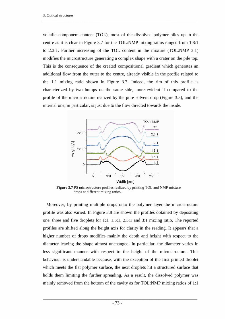
3. Optical structures ____________________________________________________________________
____________________________________________________________________ - 73 -
volatile component content (TOL), most of the dissolved polymer piles up in the
centre as it is clear in Figure 3.7 for the TOL:NMP mixing ratios ranged from 1.8:1
to 2.3:1. Further increasing of the TOL content in the mixture (TOL:NMP 3:1)
modifies the microstructure generating a complex shape with a crater on the pile top.
This is the consequence of the created compositional gradient which generates an
additional flow from the outer to the centre, already visible in the profile related to
the 1:1 mixing ratio shown in Figure 3.7. Indeed, the rim of this profile is
characterized by two humps on the same side, more evident if compared to the
profile of the microstructure realized by the pure solvent drop (Figure 3.5), and the
internal one, in particular, is just due to the flow directed towards the inside.
Figure 3.7 PS microstructure profiles realized by printing TOL and NMP mixture
drops at different mixing ratios.
Moreover, by printing multiple drops onto the polymer layer the microstructure
profile was also varied. In Figure 3.8 are shown the profiles obtained by depositing
one, three and five droplets for 1:1, 1.5:1, 2.3:1 and 3:1 mixing ratio. The reported
profiles are shifted along the height axis for clarity in the reading. It appears that a
higher number of drops modifies mainly the depth and height with respect to the
diameter leaving the shape almost unchanged. In particular, the diameter varies in
less significant manner with respect to the height of the microstructure. This
behaviour is understandable because, with the exception of the first printed droplet
which meets the flat polymer surface, the next droplets hit a structured surface that
holds them limiting the further spreading. As a result, the dissolved polymer was
mainly removed from the bottom of the cavity as for TOL:NMP mixing ratios of 1:1

3. Optical structures ____________________________________________________________________
____________________________________________________________________ - 74 -
and 1.5:1, otherwise it largely piled up in the centre as for TOL:NMP mixing ratios
of 2.3:1 and 3:1. In these last cases, the polymer microstructures can be used as
microlenses in optical structures.
Figure 3.8 Profiles of the PS microstructures manufactured by printing 1, 3 and 5
drops of TOL:NMP mixtures at volume mixing ratios (a) 1:1, (b) 1.5:1, (c) 2.3:1, and (d) 3:1.
3.2.3 .13.2.3 .13.2.3 .13.2.3 .1 O ptical characterization O ptical characterization O ptical characterization O ptical characterization via M ach via M ach via M ach via M ach----Z ehnder Z ehnder Z ehnder Z ehnder
interferom eterinterferom eterinterferom eterinterferom eter
The convex-shaped microstructures were optically investigated by means of a
Mach-Zehnder system in confocal configuration. A Mach–Zehnder interferometer is
employed because this system introduces a small measurement error being a single-
path interferometer [18]. Indeed, in general the single-path interferometer is
preferable to that double-path one (for example, Twyman–Green system) to analyze
optical components that have to be utilized in transmission mode and to reduce the
measurement errors in evaluating the microlens aberrations.
The Mach-Zehnder interferometer is schematically shown in Figure 3.9 and
described in the following. The unpolarized light coming from a He-Ne laser (534

3. Optical structures ____________________________________________________________________
____________________________________________________________________ - 75 -
nm) passes through a beam-expander; the emerged beam, after reflecting by a mirror
(M1), is divided in amplitude by a polarized beam splitter (PBS1) where the p-
polarized component is transmitted into the test path and the s-polarized component
is reflected into the reference path. The reference wave, deflected by a mirror driven
by a piezoelectric stage, passes through a half-wave plate (HWP1) to rotate its
polarized state, then through a neutral density filter and, finally, is recombined with
the test wave at a beam splitter (BS2). The test beam passes through a neutral density
to adapt the intensities of the test wave and the reference wave in order to optimize
the interferogram contrast. The test wave is focused on the under-test microstructure
by a microscope objective (MO1) in confocal position. The emerging wave is
expanded by a microscope objective (MO2), placed itself in a confocal position with
a lens (L1) and recombined with the reference wave at BS2. Finally, the light
emerging from the interferometer is collected by a further lens (L2) and sent into the
camera.
Figure 3.9 Scheme of the Mach-Zehnder interferometer system.
Since, as reported in the previous paragraph, the structure generated by five drops
of the 2.3:1 TOL:NMP mixture had the highest value of the ratio between the central
peak height and its diameter at the bottom, the interferometric analysis relative to this
specific microstructure is reported as example.

3. Optical structures ____________________________________________________________________
____________________________________________________________________ - 76 -
In Figure 3.10 is reported the three-dimensional profile of the microlens obtained
printing five drops of the 2.3:1 TOL:NMP mixture. The measurements of the
geometrical parameters by the profilometric analysis allowed to estimate the focal
length by using the following equation:
1−=
n
Rf (eq.3.1)
where n is the refractive index of the material and R is the radius of curvature and
is defined as:
L
L
h
rhR
22
2
+= (eq.3.2)
where hL is the height and r is the radius of the microlens.
For the microlenses obtained by printing five drops of the 2.3:1 TOL:NMP mixture
the focal property was equal to 1.76 mm resulting in agreement with the value
subsequently measured with the interferometric system [19].
In order to have a clear interpretation of optical test results, it is usually convenient
to express wavefront data in polynomial form. Zernike polynomials are often used
for this purpose since this component terms have the same form as the types of
aberrations usually observed in optical tests. In Figure 3.11 are shown the tilted
interferometric fringes image and the wavefront error analysis in terms of the
Zernike polynomial without the first four terms of the polynomial series for this
structure under investigation. The root-mean-square (RMS) wavefront error, which
gives information on the area over which the wavefront error is occurring, and the
peak-to-valley (P-V) wavefront aberration, namely the maximum departure of the
actual wavefront from the desired wavefront in both positive and negative directions,
were estimated equal to 1/5.08 waves and to 1/1.27 waves, respectively. These
results indicate that the central region of the analyzed structure has spherical
symmetry with low aberrations. Moreover, the lateral region of the structure having
toroidal shape also contributes to the light focusing effect but in less significant way
with respect to the central structure. Therefore, the interferometric analysis indicated
that the manufactured convex-shaped structures can be employed as good optical
quality microlenses with negligible defects.

3. Optical structures ____________________________________________________________________
____________________________________________________________________ - 77 -
Figure 3.10 3-D profile of the microlens obtained printing five drops of the 2.3:1
TOL:NMP mixture.
(a) (b)
Figure 3.11 (a) tilted interferometric fringes image and (b) wavefront error (@ λ=
550 nm) of the microlens obtained printing five drops of the 2.3:1 TOL:NMP mixture.
3.3 A pplication3.3 A pplication3.3 A pplication3.3 A pplicationssss of polym er m icrostructures to of polym er m icrostructures to of polym er m icrostructures to of polym er m icrostructures to
optoelectronic optoelectronic optoelectronic optoelectronic devicesdevicesdevicesdevices
The concave- and convex-shaped microstructures were manufactured and
characterized for different optical applications, mainly focused on the improvement
of the OLED device efficiency. The application for each realized microstructure will
be detailed in the following paragraphs.

3. Optical structures ____________________________________________________________________
____________________________________________________________________ - 78 -
3.3.1 3.3.1 3.3.1 3.3.1 PI structured by N M PPI structured by N M PPI structured by N M PPI structured by N M P in m in m in m in m ould appould appould appould app licationlicationlicationlicationssss
The structured PI layer was employed as a template for another polymer which
models itself acquiring a complementary shape. The employed polymer solution was
commercial Sylgard 184 Silicone Elastomer (Dow Corning, USA) mixed with a
curing agent and, after being placed into vacuum chamber for removing the bubbles,
spin-coated on the microstructured PI layer at 5000 rpm for 60 sec performing a
thickness of about 1 µm. Successively, after a curing process at 100 °C for 45 min,
the elastomeric silicone polymer was removed from the PI mould resulting with a
convex-shaped structuring on top of its surface, that is the complementary form with
respect to the profile of Figure 3.1.
3.3.2 3.3.2 3.3.2 3.3.2 PS structured by TO L as textured substraPS structured by TO L as textured substraPS structured by TO L as textured substraPS structured by TO L as textured substra tes in tes in tes in tes in
O L E D applicationsO L E D applicationsO L E D applicationsO L E D applications
The PS structuring with the profile shown in Figure 3.5 was employed as texturing
of the substrate of an OLED (organic light-emitting diodes) device. A detailed study
was developed demonstrating that this kind of structuring performed on a polymeric
underlayer of a bottom-emitting OLED device allows to destroy the interference
effects generated by OLED resonator cavity [20]. In the following paragraph a brief
introduction on OLEDs and on the interference effects generated in the emission
spectrum was performed.
3.3.2 .1 O L E D s: introduction and im provem ents3.3.2 .1 O L E D s: introduction and im provem ents3.3.2 .1 O L E D s: introduction and im provem ents3.3.2 .1 O L E D s: introduction and im provem ents
OLEDs are attractive for fabricating high quality, electroluminescent large area
displays and because of the potential low cost [21]. The conventional OLED
structures can differ by the architectures opportunely developed to enhance
optoelectronic device performances, lowering the electrical and optical threshold
voltages, improving the device efficiency and increasing the lifetime [22]. For

3. Optical structures ____________________________________________________________________
____________________________________________________________________ - 79 -
whatever architecture, OLEDs can be classified in two categories, bottom emitting
(BE) and top emitting (TE) [23], and in both these devices the light generated in the
emissive layer propagates through the device layers, and is emitted outside. Anyway,
more than half of the generated light is trapped and finally wasted inside the stack
due to the total internal reflections at the interfaces between layers with different
refractive-index [24]. Since the thickness of some layers of the device can be of the
same order of magnitude of the wavelength of optical radiation, interference
phenomena take place. These phenomena that produce an alteration of the emission
spectrum can be attributed to microcavity effects generated by the device that acts as
optical cavity [23,25]. In some encapsulated structures, the interference effects occur
due to the air gap between the device and the cover glass [26].
Another crucial factor that compromises OLED luminance efficiency is the surface
roughness of anode contact, leading to the formation of dark spots, degradation, and
hence to failure of the device working. Many efforts have been made to improve
OLED performances modifying the anodic layer surface through chemical and
physical treatments [27], or introducing a polymer layer directly under the electrode
[28]. As concerning this last approach, the right choice of the polymer material to
realize the under-layer allows of optimizing the visible light transmittance, matching
the refractive indices of adjacent layers, and enhancing the device stability [28,29].
In this thesis work, BE OLED devices fabricated onto a polymer layer spin-coated
on glass substrate. The polymer film smoothes the anode surface reducing its
roughness. Anyway, as the polymer under-layer is thin, interference effects take
place modifying the OLED emission spectrum. In order to eliminate this
phenomenon a method based on the structuring of polymer under-layer surface by
means of the inkjet printing technology is proposed.
3.3.2 .2 O L E D device fabrication3.3.2 .2 O L E D device fabrication3.3.2 .2 O L E D device fabrication3.3.2 .2 O L E D device fabrication
The PS layer is introduced in OLED devices as under-layer in order to improve the
roughness of the anodic electrode so enhancing the electroluminescence
performances.

3. Optical structures ____________________________________________________________________
____________________________________________________________________ - 80 -
ZnO (zinc oxide) films were sputtered onto PS/glass system and, as comparison,
directly on glass. The morphology of the conductive films were analyzed by an
atomic force microscopy (AFM) (Veeco, Dimension Digital Instruments Nanoscope
IV) and reported in Figure 3.12. The 3D-topography images and the related mean
roughness values indicated that the polymer reduces the roughness degree of the
oxide film deposited on it. Hence, the insertion of the PS layer improves the ZnO
electrode morphological properties for OLED applications.
0.10.2
0.30.4
0.5
µµµµm
0.10.2
0.30.4
0.5µµµµm
(a) Ra = 0.56 nm (b) Ra = 1.05 nm0.10.2
0.30.4
0.5
µµµµm
0.10.2
0.30.4
0.5µµµµm
(a) Ra = 0.56 nm (b) Ra = 1.05 nm Figure 3.12 AFM images (scan size 0.5x0.5 µm2, z scale 10 nm) of ZnO films
sputtered on PS/glass (a) and directly on glass (b). Ra is the average roughness value.
Successively, the double-layer OLED device with ZnO/NPD (N,N-Di-[(1-
naphthalenyl)-N,N-diphenyl]-1,1-biphenyl-4,4-diamine)/Alq3 (tris 8-
hydroxyquinoline aluminium salt)/Al (aluminium) structure was manufactured on PS
film. The ZnO anodic contact (240 nm, 26.9 Ω/square, nZnO = 1.89 @ λ = 500 nm)
was deposited in a MRC643 system (4 mTorr, 2.2 W/cm2) by RF sputtering (13.56
MHz) from a Al2O3 doped ZnO target in Ar-plasma atmosphere. NPD and Alq3, 40
nm and 60 nm thick, respectively, were deposited by thermal evaporation without
breaking vacuum conditions (10-7 mbar base pressure). The aluminium cathode (200
nm) was evaporated as a final layer. The active device area was 0.56 mm2.
In Figure 3.13 is reported a schematic image of the device stack.

3. Optical structures ____________________________________________________________________
____________________________________________________________________ - 81 -
Figure 3.13 Schematic section of OLED stack manufactured on a polymeric under-
layer.
3.3.2 .33.3.2 .33.3.2 .33.3.2 .3 Interference effects in an optical cavity Interference effects in an optical cavity Interference effects in an optical cavity Interference effects in an optical cavity
The electroluminescence (EL) spectra emitted by the realized OLED devices was
detected employing a CCD-telescope to collect and send the light to a
spectroradiometer through optical fibre (Optronics Laboratories OL770 system).
These measurements were performed also at different angles by holding the OLED
device on a goniometric system and placing it in front of the CCD. OLED emission
spectra detected at different angles are shown in Figure 3.14.
Figure 3.14 Emission spectra of OLED on the unstructured PS under-layer at
different view angles. The inset curves are obtained subtracting the spectra interpolation to detected EL profiles.
Interference effects occur at different wavelengths for each investigated angle and
can give many information about the PS layer and the properties of the light source.
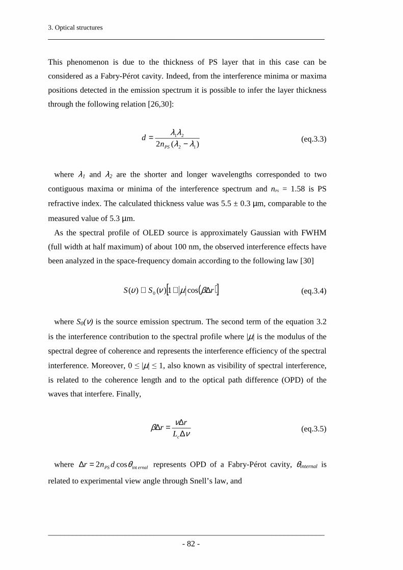
3. Optical structures ____________________________________________________________________
____________________________________________________________________ - 82 -
This phenomenon is due to the thickness of PS layer that in this case can be
considered as a Fabry-Pérot cavity. Indeed, from the interference minima or maxima
positions detected in the emission spectrum it is possible to infer the layer thickness
through the following relation [26,30]:
)(2 12
21
λλλλ
−=
PSnd (eq.3.3)
where λ1 and λ2 are the shorter and longer wavelengths corresponded to two
contiguous maxima or minima of the interference spectrum and nPS = 1.58 is PS
refractive index. The calculated thickness value was 5.5 ± 0.3 µm, comparable to the
measured value of 5.3 µm.
As the spectral profile of OLED source is approximately Gaussian with FWHM
(full width at half maximum) of about 100 nm, the observed interference effects have
been analyzed in the space-frequency domain according to the following law [30]
( )[ ]rSS ∆+∝ βµνυ cos1)()( 0 (eq.3.4)
where S0(ν) is the source emission spectrum. The second term of the equation 3.2
is the interference contribution to the spectral profile where |µ| is the modulus of the
spectral degree of coherence and represents the interference efficiency of the spectral
interference. Moreover, 0 ≤ |µ| ≤ 1, also known as visibility of spectral interference,
is related to the coherence length and to the optical path difference (OPD) of the
waves that interfere. Finally,
ννβ
∆∆=∆
cL
rr (eq.3.5)
where ernalPS dnr intcos2 θ=∆ represents OPD of a Fabry-Pérot cavity, θinternal is
related to experimental view angle through Snell’s law, and

3. Optical structures ____________________________________________________________________
____________________________________________________________________ - 83 -
λπλ∆
=ps
c nL
22ln2
(eq.3.6)
is the coherence length of a light source. In the examined case, the emission peak
wavelength (λ ) is centered at 525 nm with nm100=∆λ and Lc results equal to 0.77
µm. By using the parameters that characterizes the realized Fabry-Pérot cavity, the
theoretical calculations give |µ| ~ 0.1. This low value of |µ| explains the reduced
visibility of the interference effect in spectral profile of the OLED source.
The interference effect was more evident in the configuration with the device
placed in front of the detector with respect to the other angular positions as pointed
out by the emission profiles showed in the inset of Figure 3.14 and obtained
subtracting the interpolation of EL profile to the detected spectrum for each view
angle. As the detection angle increases, OPD decreases and the fringes broaden and
their intensity reduces.
Anyhow, the interference effect still visible at 30° was observed also at higher
angles depending on the particular realized Fabry-Perot cavity, and, hence, on the
structure geometry and on the materials optical properties.
All the reported results show that the PS under-layer has good optical properties in
visible range, reduces the roughness degree of the anodic electrode deposited on it,
nevertheless introduces an interference phenomenon, modifying the OLED emission
spectrum. A structuring of PS was used in order to solve this phenomenon.
For this reason, a square array of microcavities was fabricated by printing TOL
multiple drops on the PS film and than the OLED device was fabricated on the top of
structured PS layer. The related schematic section and optical micrograph are
reported in Figure 3.15.

3. Optical structures ____________________________________________________________________
____________________________________________________________________ - 84 -
(a) (b)
(c)
Figure 3.15 (a) Schematic section and (b) optical micrograph of a PS microcavities
array. (c) Schematic section of OLED stack manufactured on structured polymer underlayer
The structured OLED emission spectra at different view angles are shown in Figure
3.16.
The emission profile clearly exhibits a strongly reduced, almost absent interference
effect upon the under-layer structuring. This can be attributed to the locally reduced
thickness of the textured polymer layer and to the interface shape that randomizes the
lightpath. The inset of Figure 3.16 points out that only a slight interference effect is
still visible in the structured OLED EL profile due to the presence of untextured
areas of PS layer. Indeed, the distance between two contiguous cavities of the array
is about 10 µm.
The polymer structuring allows to ensure the morphological benefits of the anodic
contact that retains a local low roughness and, at the same time, to assure that the
emitted spectrum is only function of the emitting source and is not affected by the
presence of the polymer under-layer.

3. Optical structures ____________________________________________________________________
____________________________________________________________________ - 85 -
Figure 3.16 Structured OLED emission spectra for different detection angles. The
measured EL profile minus the spectrum interpolation is detailed in the inset for each angle.
3.3.3 3.3.3 3.3.3 3.3.3 PS structured by TO L :N M P as m icrolePS structured by TO L :N M P as m icrolePS structured by TO L :N M P as m icrolePS structured by TO L :N M P as m icrolenses nses nses nses O L E D O L E D O L E D O L E D
applicationapplicationapplicationapplicationssss
The convex-shaped microstructures manufactured with the TOL:NMP-PS system
can be used as microlenses in order to reduce the electroluminescence (EL) radiation
losses due to the total internal reflection in an OLED device.
To cover the entire area of the OLED device, a square array of microlenses was
fabricated with a 5x5 mm2 surface by printing one, three and five drops of the 2.3:1
TOL:NMP on the PS layer. In Figure 3.17 the schematic section and the optical
micrograph of the PS microlens array are illustrated.
(a) (b)
Figure 3.17 Schematic section (a) and optical micrograph (b) of a PS microlens array.

3. Optical structures ____________________________________________________________________
____________________________________________________________________ - 86 -
In Figure 3.18a is illustrated the schematic section of the OLED stack coupled to
the microlens array which was fabricated on the opposite side of the substrate. The
current-tension characteristic illustrated in Figure 3.18b was the typical electrical
response measured for all the manufactured devices, both coupled and not coupled to
microlenses. The OLEDs showed good electrical performances (VON ~ 3 V) and
good detected reproducibility which was crucial to study the functioning of the
microlenses and to compare the efficiencies of the different arrays. To this end, in
Figure 3.19 are reported the curves of the photodiode current as function of the
electrical current for the OLEDs coupled to different microlens arrays and, as
comparison, for the unlensed OLED, namely the device manufactured with the same
stack and with an unstructured PS layer on the opposite side of the substrate. The
results pointed out that the OLED electroluminescence efficiency was enhanced by
applying the microlenses. In detail, by tuning the number of drops the curvature
radius of the microlenses was controlled and so also their focal length. By coupling
these lens systems to the OLED, the device efficiency was improved by a factor
ranging from 2.2 % to 5 %. The lenses manufactured by five drops provided the
highest EL efficiency, nevertheless this enhance was weak with respect to the
efficiency detected for the device without lenses due to the lens geometry, i.e. the
ratio between the microstructure height and its diameter as low as 1.62 %, that means
long focal length. However, although the maximum obtained electroluminescence
efficiency enhance was not significantly high, it is worth noting the trend of the
increase of the EL efficiency as the ratio between the height (of the central peak) and
the diameter (at the bottom) increases.
(a) (b)
Figure 3.18 (a) Schematic section of the OLED stack coupled to the microlens array
and (b) typical I-V curve of all the manufactured devices.
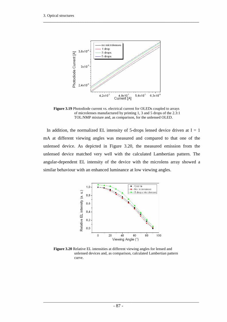
3. Optical structures ____________________________________________________________________
____________________________________________________________________ - 87 -
Figure 3.19 Photodiode current vs. electrical current for OLEDs coupled to arrays
of microlenses manufactured by printing 1, 3 and 5 drops of the 2.3:1 TOL:NMP mixture and, as comparison, for the unlensed OLED.
In addition, the normalized EL intensity of 5-drops lensed device driven at I = 1
mA at different viewing angles was measured and compared to that one of the
unlensed device. As depicted in Figure 3.20, the measured emission from the
unlensed device matched very well with the calculated Lambertian pattern. The
angular-dependent EL intensity of the device with the microlens array showed a
similar behaviour with an enhanced luminance at low viewing angles.
Figure 3.20 Relative EL intensities at different viewing angles for lensed and
unlensed devices and, as comparison, calculated Lambertian pattern curve.

3. Optical structures ____________________________________________________________________
____________________________________________________________________ - 88 -
3.4 M icrolens fabrication via additive m ethod3.4 M icrolens fabrication via additive m ethod3.4 M icrolens fabrication via additive m ethod3.4 M icrolens fabrication via additive m ethod
The previously described technique (IJE) provide a method for fabricating polymer
microstructures that were employed as microlenses in OLED devices. Anyway, this
technique doesn’t allow to significantly vary the ratio between the height and the
diameter of the microstructures. Therefore, another approach based on the additive
deposition of optical grade polymer materials was followed in order to realize
refractive microlenses which can be more efficiently applied in several application
fields such as communications, display systems, imaging sensors, photodetectors.
Therefore, many methods have been developed to fabricate these optical
components. Traditional fabrication techniques use photolithography [31], resist
processing [32], reactive ion etching [33], laser irradiation [34] while other, more
recent techniques are based on microjet printing [35], direct laser [36] or e-beam
writing [37], laser ablation [38], photopolymerization [39]. All these methods
produce optical quality microlenses, namely characterized by low aberration and
good uniformity of the focal length. However, only some of these techniques are
suitable for rapid prototyping of microlenses with variable focal length, generally
those ones that don’t need to employ masks, resulting less complex and short time-
consuming processes which, hence, allow to reduce the production costs.
The inkjet printing is one of the techniques that satisfy these requirements;
moreover, it offers also other advantages such as the versatility in definition of the
patterns and in the employable substrates and the potentiality to be introduced in roll-
to-roll processes. The employment of the IJP technology to fabricate optical elements
was essentially promoted by the development of optical grade polymers with suitable
thermal and mechanical properties [19,40]. On the other hand, the right combination
of using these materials with a low-cost technology was further supported for
manufacturing less expensive and more lightweight components.
Among the most commonly used polymers for the fabrication of optical
components, poly(methyl methacrylate) (PMMA) is an optical grade polymer with
good mechanical and thermal properties. In particular, this polymer was employed to
manufacture microlenses through printing methods [41,42], nevertheless no
systematic study is reported about the effects of the chemico-physical properties of
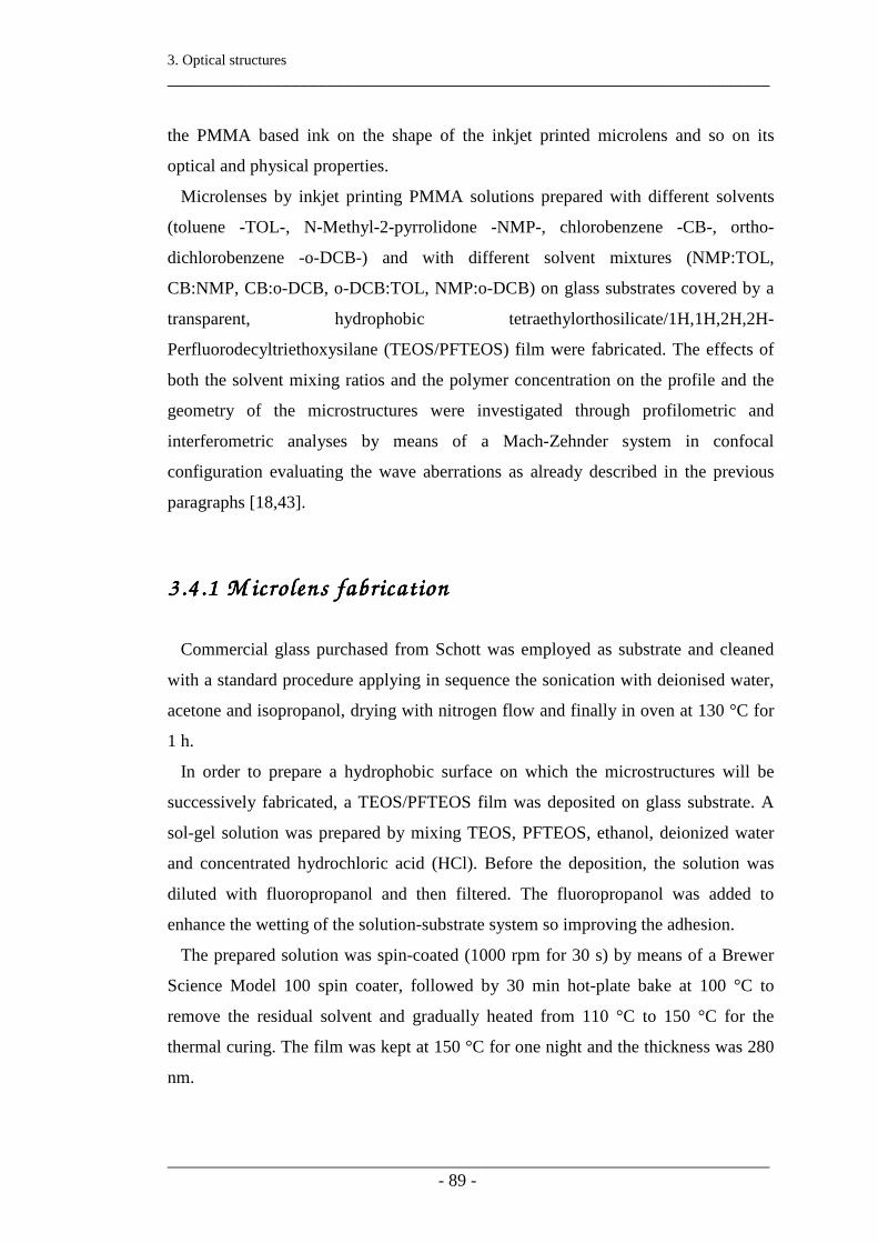
3. Optical structures ____________________________________________________________________
____________________________________________________________________ - 89 -
the PMMA based ink on the shape of the inkjet printed microlens and so on its
optical and physical properties.
Microlenses by inkjet printing PMMA solutions prepared with different solvents
(toluene -TOL-, N-Methyl-2-pyrrolidone -NMP-, chlorobenzene -CB-, ortho-
dichlorobenzene -o-DCB-) and with different solvent mixtures (NMP:TOL,
CB:NMP, CB:o-DCB, o-DCB:TOL, NMP:o-DCB) on glass substrates covered by a
transparent, hydrophobic tetraethylorthosilicate/1H,1H,2H,2H-
Perfluorodecyltriethoxysilane (TEOS/PFTEOS) film were fabricated. The effects of
both the solvent mixing ratios and the polymer concentration on the profile and the
geometry of the microstructures were investigated through profilometric and
interferometric analyses by means of a Mach-Zehnder system in confocal
configuration evaluating the wave aberrations as already described in the previous
paragraphs [18,43].
3.4.1 M icrolens fabrication3.4.1 M icrolens fabrication3.4.1 M icrolens fabrication3.4.1 M icrolens fabrication
Commercial glass purchased from Schott was employed as substrate and cleaned
with a standard procedure applying in sequence the sonication with deionised water,
acetone and isopropanol, drying with nitrogen flow and finally in oven at 130 °C for
1 h.
In order to prepare a hydrophobic surface on which the microstructures will be
successively fabricated, a TEOS/PFTEOS film was deposited on glass substrate. A
sol-gel solution was prepared by mixing TEOS, PFTEOS, ethanol, deionized water
and concentrated hydrochloric acid (HCl). Before the deposition, the solution was
diluted with fluoropropanol and then filtered. The fluoropropanol was added to
enhance the wetting of the solution-substrate system so improving the adhesion.
The prepared solution was spin-coated (1000 rpm for 30 s) by means of a Brewer
Science Model 100 spin coater, followed by 30 min hot-plate bake at 100 °C to
remove the residual solvent and gradually heated from 110 °C to 150 °C for the
thermal curing. The film was kept at 150 °C for one night and the thickness was 280
nm.

3. Optical structures ____________________________________________________________________
____________________________________________________________________ - 90 -
Successively, the polymeric inks were prepared by dissolving 5 mg/mL of PMMA
in different solvents, such as TOL, NMP, CB and DCB, and in different solvent
mixtures, such as NMP:TOL, CB:NMP, CB:DCB, DCB:TOL and NMP:DCB. All
the solvent mixture systems were investigated at volume mixing ratios of 20:80 and
80:20. Additionally, solutions of PMMA (40 mg/mL) in pure NMP and NMP:TOL
mixture (80:20) were also investigated. All the chosen solvents are suitable to
dissolve the polymer and have right volatility and surface tension properties for
inkjet printing processing (TOL: Tb = 110.6 °C, γ = 28.53 mN/m; NMP: Tb = 202 °C,
γ = 40 mN/m; CB: Tb = 132 °C, γ = 33.6 mN/m; DCB: Tb = 180 °C, γ = 26.84
mN/m).
Polymeric microstructures were fabricated by printing single drops of the PMMA
based inks on the hydrophobic surface of the TEOS/PFTEOS film in order to freeze
the drop on the substrate so minimizing the spreading.
The droplet depositions were performed by using Microdrop printhead with 30 µm
opening nozzle corresponding to 20 pL droplet volume. During the printing process,
the substrate temperature was kept at 17 °C by means of a Peltier cell and monitored
by a thermocouple. The prints were carried out at 110 Hz drop emission frequency
and 10 mm/s printhead speed.
After printing, the PMMA microstructures were left at 17 °C for 30 min for
completing the polymer drying.
A surface profilometer (KLA Tencor P-10 Surface Profiler) was used to detect the
profile and the geometry of the manufactured microstructures while a Mach-Zehnder
interferometer was employed to evaluate the wave aberrations [44].
3.4.23.4.23.4.23.4.2 M icrolens characterization M icrolens characterization M icrolens characterization M icrolens characterization
The profiles of the PMMA microstructures realized by employing five different
solvent mixtures, each one with two mixing ratios (20:80 and 80:20), are shown in
Figure 3.21 and compared with those obtained by the pure component solvents.
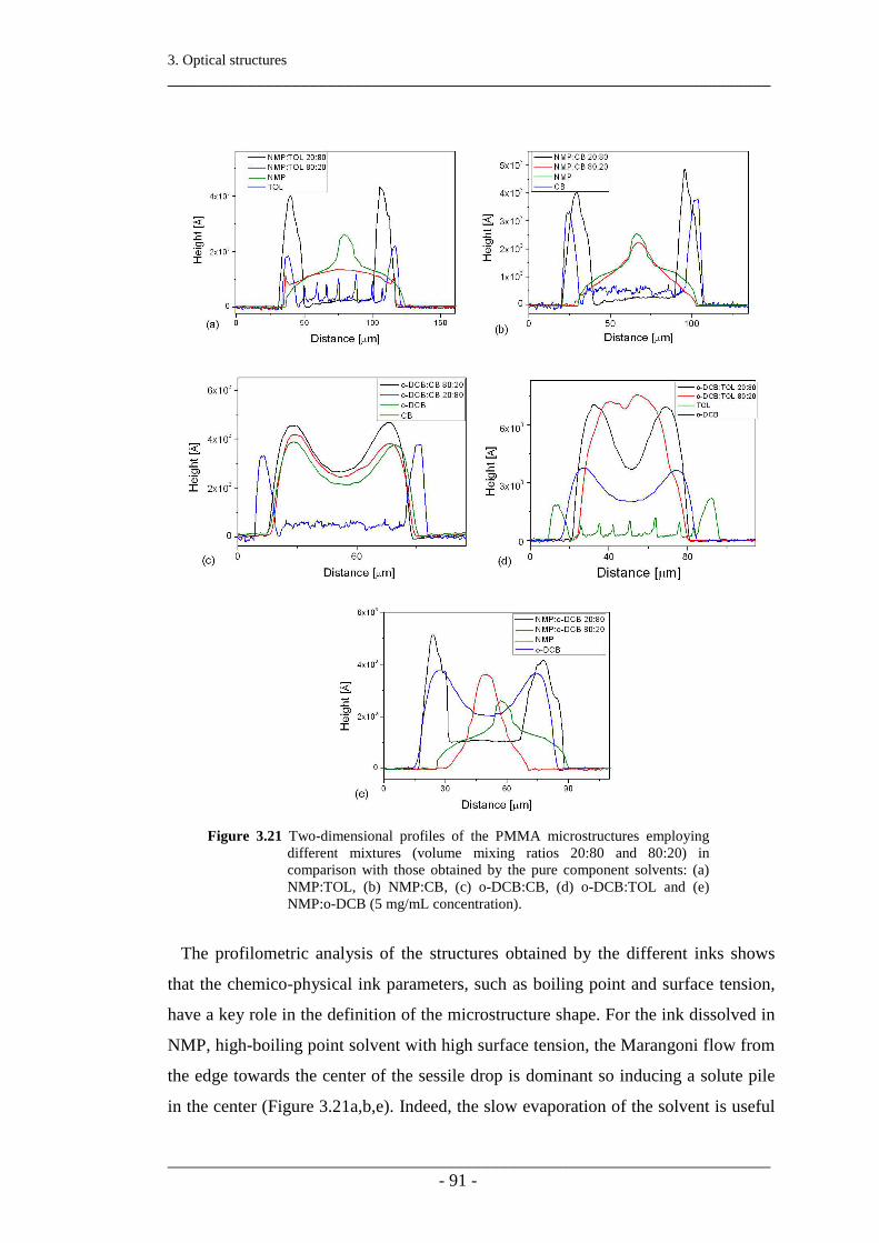
3. Optical structures ____________________________________________________________________
____________________________________________________________________ - 91 -
Figure 3.21 Two-dimensional profiles of the PMMA microstructures employing
different mixtures (volume mixing ratios 20:80 and 80:20) in comparison with those obtained by the pure component solvents: (a) NMP:TOL, (b) NMP:CB, (c) o-DCB:CB, (d) o-DCB:TOL and (e) NMP:o-DCB (5 mg/mL concentration).
The profilometric analysis of the structures obtained by the different inks shows
that the chemico-physical ink parameters, such as boiling point and surface tension,
have a key role in the definition of the microstructure shape. For the ink dissolved in
NMP, high-boiling point solvent with high surface tension, the Marangoni flow from
the edge towards the center of the sessile drop is dominant so inducing a solute pile
in the center (Figure 3.21a,b,e). Indeed, the slow evaporation of the solvent is useful

3. Optical structures ____________________________________________________________________
____________________________________________________________________ - 92 -
so that the Marangoni flow diffuses from regions with low surface tension to regions
with high surface tension, these last ones located around the top center of the droplet.
For all the other investigated solvents with lower boiling point and lower surface
tension lower than those ones of NMP, the drying process is mainly ruled by the flow
of the “coffee-stain effect” and the final profiles are characterized by a flat central
portion and two lateral humps. In particular, DCB, higher-boiling point solvent than
TOL and CB, induces a partial inward flow. Indeed, for DCB the ratio between the
lateral hump height and the flat central portion height is lower if compared with
those of TOL and CB.
By employing the solvent mixtures, at the end of the drying process the PMMA
microstructure profile is similar to that induced by the component solvent which is
present in the mixture with higher concentration. By examining case by case, the
DCB:CB mixture in both the volume mixing ratios 80:20 and 20:80 (Figure 3.21c)
doesn’t modify the profile obtained by DCB in significant manner being the
chemico-physical properties of the component solvents almost similar. For the
DCB:TOL mixture with 80:20 mixing ratio (Figure 3.21d), the microstructure profile
shows a larger accumulation at the centre with respect the profiles by pure DCB and
pure TOL. This behaviour is expected since the component solvent with higher
boiling-point (o-DCB) with respect to the solvent with lower boiling-point (TOL) has
also got a lower surface tension than the other one, so inducing an inward flow.
Finally, by analyzing the NMP:TOL, NMP:CB and NMP:o-DCB mixtures at 80:20
mixing ratio (Figure 3.21a,b,e), the presence of the solvent with lower boiling point
in comparison NMP lightly enhances the outward flow due to “coffee-stain effect”
making the central pile, which is evident in the profile generated by NMP, less
pronounced.
This analysis showed that the solvent in which the polymer is dissolved allows to
control the microstructure profile. In particular, among all the investigated solvent
systems both the pure NMP solvent and the NMP:TOL mixture (80:20) are the most
suitable to perform convex-shaped microstructures to be employed as optical
components.
In order to investigate if it is possible to improve the spherical symmetry of the
structures, the effect of the ink viscosity on the microstructure shape was studied.

3. Optical structures ____________________________________________________________________
____________________________________________________________________ - 93 -
The attention was focused on the solutions obtained dissolving PMMA in pure NMP
and in NMP:TOL mixture (80:20) and prepared the inks by increasing the polymer
concentration from 5 mg/mL to 40 mg/mL. The 2-dimensional profiles of the
microstructures obtained by printing the single drop for both these inks are shown in
Figure 3.22. By comparing these results with the profiles of the same inks prepared
at lower PMMA concentration (Figure 3.21b,c), it appears that the higher
concentration improves the spherical shape of the microstructures for both the
investigated systems. Moreover, the effect of the ink viscosity on the microstructure
profile is more significant than the volume mixing ratio so resulting a fundamental
parameter to manufacture structures that have to be employed as microlenses.
(a)
(b) (c)
Figure 3.22 Two-dimensional profiles obtained by printing PMMA dissolved in pure NMP and NMP:TOL mixture (80:20) (40 mg/mL concentration) (a), pure NMP at 50 and 200mg/mL (b) and NMP:TOL 80:20 at 50 and 200 mg/mL(c).
By profilometric analysis of the microlenses manufactured at higher concentration,
the geometrical parameters, namely diameter and height were evaluated, and the
focal length was calculated[19]. The focal lengths were extimated equal to 82 µm
and 442 µm for pure NMP and NMP:TOL mixture, respectively.

3. Optical structures ____________________________________________________________________
____________________________________________________________________ - 94 -
These microstructures were also analyzed by means of a Mach-Zehnder system in
confocal configuration as described in 3.2.3.1 section. The results of the
interferometric analysis are reported in Figure 3.23 for pure NMP and in Figure 3.24
for NMP:TOL mixture.
Figure 3.23 (a) 3-D image, (b) tilted interferometric fringes image and (c) wavefront error of the microlens by printing PMMA dissolved in pure NMP (40 mg/mL concentration).
Figure 3.24 (a) 3-D image, (b) tilted interferometric fringes image and (c) wavefront error of the microlens by printing PMMA dissolved in NMP:TOL mixture (80:20) (40 mg/mL concentration).
These figures illustrate the 3-D profiles (Figure 3.23a, Figure 3.24a), tilted
interferometric fringes images (Figure 3.23b, Figure 3.24b) and the wavefront error
analysis in terms of the Zernike polynomial without the first four terms of the
polynomial series (Figure 3.23c, Figure 3.24c). As previously explained, Zernike
polynomials are used to describe the aberrations of lenses with respect to an ideal
spherical shape in terms of RMS wavefront error and peak-to-valley (P-V) wavefront
aberration [44]. For microlens by pure NMP, the RMS wavefront error was 1/5.18
waves and peak-to-valley (P-V) wavefront aberration resulted 1/4.55 waves. For
microlens by NMP:TOL mixture (80:20), the RMS wavefront error was 1/15.1
waves and peak-to-valley (P-V) wavefront aberration was 1/3.011 waves. These
results obtained for the microstructure by pure NMP show high optical quality.
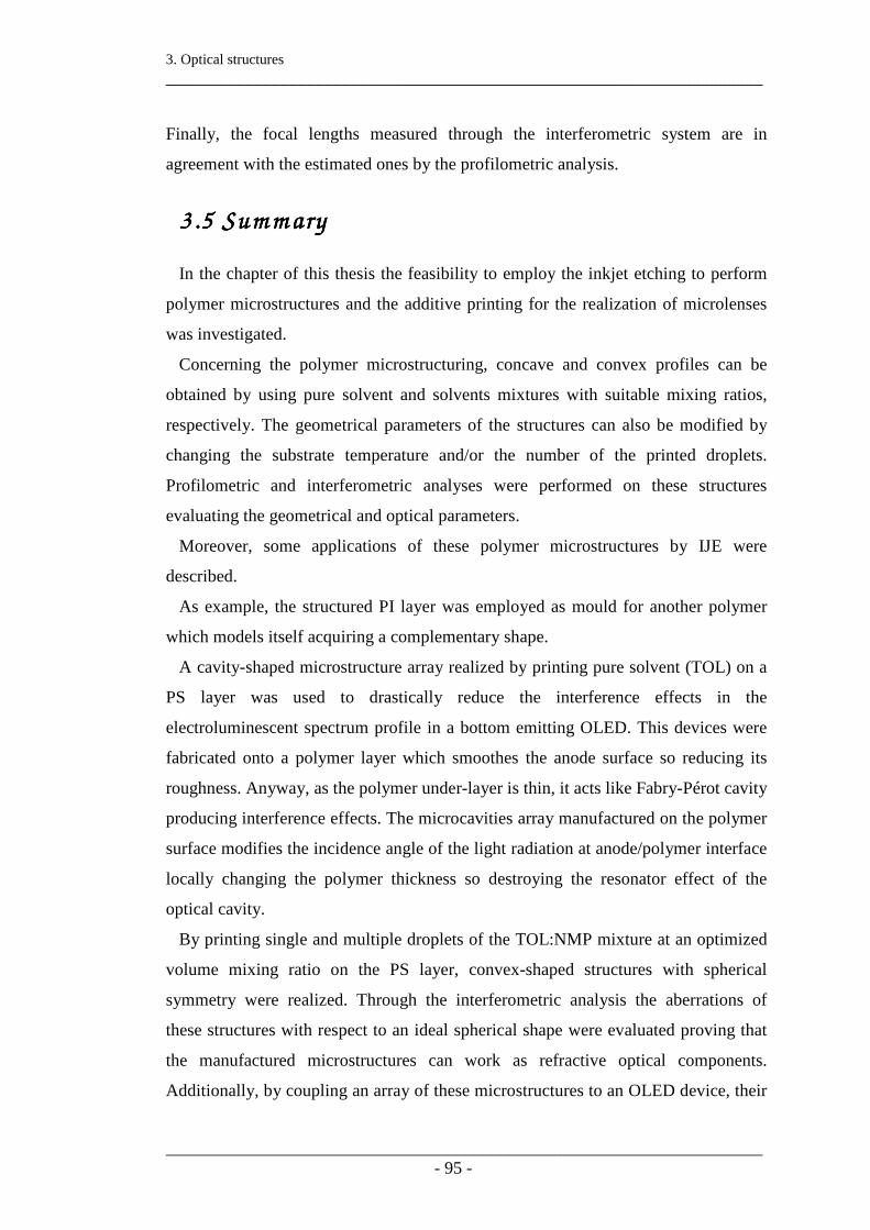
3. Optical structures ____________________________________________________________________
____________________________________________________________________ - 95 -
Finally, the focal lengths measured through the interferometric system are in
agreement with the estimated ones by the profilometric analysis.
3.5 S3.5 S3.5 S3.5 Sum m aryum m aryum m aryum m ary
In the chapter of this thesis the feasibility to employ the inkjet etching to perform
polymer microstructures and the additive printing for the realization of microlenses
was investigated.
Concerning the polymer microstructuring, concave and convex profiles can be
obtained by using pure solvent and solvents mixtures with suitable mixing ratios,
respectively. The geometrical parameters of the structures can also be modified by
changing the substrate temperature and/or the number of the printed droplets.
Profilometric and interferometric analyses were performed on these structures
evaluating the geometrical and optical parameters.
Moreover, some applications of these polymer microstructures by IJE were
described.
As example, the structured PI layer was employed as mould for another polymer
which models itself acquiring a complementary shape.
A cavity-shaped microstructure array realized by printing pure solvent (TOL) on a
PS layer was used to drastically reduce the interference effects in the
electroluminescent spectrum profile in a bottom emitting OLED. This devices were
fabricated onto a polymer layer which smoothes the anode surface so reducing its
roughness. Anyway, as the polymer under-layer is thin, it acts like Fabry-Pérot cavity
producing interference effects. The microcavities array manufactured on the polymer
surface modifies the incidence angle of the light radiation at anode/polymer interface
locally changing the polymer thickness so destroying the resonator effect of the
optical cavity.
By printing single and multiple droplets of the TOL:NMP mixture at an optimized
volume mixing ratio on the PS layer, convex-shaped structures with spherical
symmetry were realized. Through the interferometric analysis the aberrations of
these structures with respect to an ideal spherical shape were evaluated proving that
the manufactured microstructures can work as refractive optical components.
Additionally, by coupling an array of these microstructures to an OLED device, their

3. Optical structures ____________________________________________________________________
____________________________________________________________________ - 96 -
functioning as microlenses was specifically investigated. It was observed an increase
of the electroluminescence efficiency of the lensed devices as the focal length
decreased, up to a maximum of 5 % with respect to the unlensed device. Moreover,
the analysis of the angular-dependent EL intensity showed that the devices with and
without lenses had a Lambertian behavior with an increased light focalizing effect by
the lensed device at low viewing angles.
The last part of this chapter was focused on the realization and characterization of
microlenses obtained by means additive printing of PMMA droplet on a hydrophobic
substrate. The microstructure profile was controlled by employing pure solvents and
solvent mixtures with different mixing ratios. The influence of the chemico-physical
parameters of the ink, such as boiling point and surface tension, on the structure
shape was investigated as responsible parameters of more or less significant “coffee-
stain effect” with respect to the Marangoni effect. Moreover, the effect of the
polymer viscosity on the microstructure profile was studied: the results showed that
the ink prepared with higher concentration of the polymer improves the spherical
shape of the microstructures for both the pure solvent and solvent mixture systems.
Additionally, the interferometric analysis allowed to evaluate the aberrations of the
realized microlenses with respect to an ideal spherical shape and the results
demonstrated that the right choice of the solvent and the polymer concentration in
preparing the ink lead to high optical quality microlenses.

3. Optical structures ____________________________________________________________________
____________________________________________________________________ - 97 -
B ibliography B ibliography B ibliography B ibliography [1] S. Bouaidat, C. Berendsen, P. Thomsen, S.G. Petersen, A. Wolff, J. Jonsmann,
Micro patterning of cell and protein non-adhesive plasma polymerized coatings for biochip applications, Lab Chip. 4 (2004) 632.
[2] J. Hyun, H. Ma, Z. Zhang, T.P. Beebe Jr., A. Chilkoti, Universal Route to Cell Micropatterning Using an Amphiphilic Comb Polymer, Advanced Materials. 15 (2003) 576-579.
[3] Y. Xia, R.H. Friend, Nonlithographic patterning through inkjet printing via holes, Appl. Phys. Lett. 90 (2007) 253513.
[4] C.Y. Chang, S.Y. Yang, J.L. Sheh, A roller embossing process for rapid fabrication of microlens arrays on glass substrates, Microsyst Technol. 12 (2006) 754-759.
[5] R. Pericet-Camara, A. Best, S.K. Nett, J.S. Gutmann, E. Bonaccurso, Arrays of microlenses with variable focal lengths fabricated by restructuring polymer surfaces with an ink-jet device, Opt Express. 15 (2007) 9877-9882.
[6] R. Kapur, B.J. Spargo, M. Chen, J.M. Calvert, A.S. Rudolph, Fabrication and selective surface modification of 3dimensionally textured biomedical polymers from etched silicon substrates, Journal of Biomedical Materials Research. 33 (1996) 205-216.
[7] W.-K. Huang, W.-S. Wang, H.-C. Kan, F.-C. Chen, Enhanced Light Out-Coupling Efficiency of Organic Light-Emitting Diodes with Self-Organized Microlens Arrays, Jpn. J. Appl. Phys. 45 (2006) L1100-L1102.
[8] A.J. Lennon, A.W.Y. Ho-Baillie, S.R. Wenham, Direct patterned etching of silicon dioxide and silicon nitride dielectric layers by inkjet printing, Solar Energy Materials and Solar Cells. 93 (2009) 1865-1874.
[9] R.D. Deegan, O. Bakajin, T.F. Dupont, G. Huber, S.R. Nagel, T.A. Witten, Capillary flow as the cause of ring stains from dried liquid drops, Nature. 389 (1997) 827-829.
[10] R.D. Deegan, Pattern formation in drying drops, Phys. Rev. E. 61 (2000) 475.
[11] R.D. Deegan, O. Bakajin, T.F. Dupont, G. Huber, S.R. Nagel, T.A. Witten, Contact line deposits in an evaporating drop, Phys. Rev. E. 62 (2000) 756.
[12] B.-J. de Gans, S. Hoeppener, U.S. Schubert, Polymer relief microstructures by inkjet etching, J. Mater. Chem. 17 (2007) 3045.
[13] B. J de Gans, S. Hoeppener, U.S. Schubert, Polymer-Relief Microstructures by Inkjet Etching, Advanced Materials. 18 (2006) 910-914.
[14] T. Kawase, H. Sirringhaus, R.H. Friend, T. Shimoda, Inkjet Printed ViaHole Interconnections and Resistors for AllPolymer Transistor Circuits, Advanced Materials. 13 (2001) 1601-1605.
[15] E. Bonaccurso, H.-J. Butt, B. Hankeln, B. Niesenhaus, K. Graf, Fabrication of microvessels and microlenses from polymers by solvent droplets, Appl. Phys. Lett. 86 (2005) 124101.
[16] E. Tekin, E. Holder, D. Kozodaev, U.S. Schubert, Controlled Pattern Formation of Poly[2-methoxy-5-(2′-ethylhexyloxyl)–1,4-phenylenevinylene]

3. Optical structures ____________________________________________________________________
____________________________________________________________________ - 98 -
(MEH–PPV) by Ink-Jet Printing, Advanced Functional Materials. 17 (2007) 277-284.
[17] H. Hu, R.G. Larson, Marangoni Effect Reverses Coffee-Ring Depositions, The Journal of Physical Chemistry B. 110 (2006) 7090-7094.
[18] T. Miyashita, Standardization for Microlenses and Microlens Arrays, Jpn. J. Appl. Phys. 46 (2007) 5391-5396.
[19] C.-T. Chen, C.-L. Chiu, Z.-F. Tseng, C.-T. Chuang, Dynamic evolvement and formation of refractive microlenses self-assembled from evaporative polyurethane droplets, Sensors and Actuators A: Physical. 147 (2008) 369-377.
[20] F. Villani, I.A. Grimaldi, G. Nenna, A.D.G. Del Mauro, F. Loffredo, C. Minarini, Study of the interference effects in an optical cavity for organic light-emitting diode applications, Opt. Lett. 35 (2010) 3333-3335.
[21] J.H. Burroughes, D.D.C. Bradley, A.R. Brown, R.N. Marks, K. Mackay, R.H. Friend, et al., Light-emitting diodes based on conjugated polymers, Nature. 347 (1990) 539-541.
[22] S.R. Forrest, The road to high efficiency organic light emitting devices, Organic Electronics. 4 (2003) 45-48.
[23] C.J. Lee, R.B. Pode, D.G. Moon, J.I. Han, N.H. Park, S.H. Baik, et al., On the problem of microcavity effects on the top emitting OLED with semitransparent metal cathode, Physica Status Solidi (a). 201 (2004) 1022-1028.
[24] Weixin Li, R.A. Jones, S.C. Allen, J.C. Heikenfeld, A.J. Steckl, Maximizing Alq/sub 3/ OLED internal and external efficiencies: charge balanced device structure and color conversion outcoupling lenses, Journal of Display Technology. 2 (2006) 143-152.
[25] V. Cimrová, D. Neher, Microcavity effects in single-layer light-emitting devices based on poly(p-phenylene vinylene), J. Appl. Phys. 79 (1996) 3299.
[26] D. Hill, K. Leo, G. He, Q. Huang, Analysis of spatial coherence of organic light-emitting devices through investigation of interference effects observed in top-emitting devices, Appl. Phys. Lett. 90 (2007) 101111.
[27] P. Vacca, M. Petrosino, A. Guerra, R. Chierchia, C. Minarini, D.D. Sala, et al., The Relation between the Electrical, Chemical, and Morphological Properties of Indium−Tin Oxide Layers and Double-Layer Light-Emitting Diode Performance, The Journal of Physical Chemistry C. 111 (2007) 17404-17408.
[28] H.-C. Hsieh, S.-C. Chang, Y.-M. Tsai, P-73: ITO Characteristics on Different Under-Layer for AM-OLED Displays, SID Symposium Digest. 34 (2003) 498-501.
[29] B.J. Chen, X.W. Sun, B.K. Tay, L. Ke, S.J. Chua, Improvement of efficiency and stability of polymer light-emitting devices by modifying indium tin oxide anode surface with ultrathin tetrahedral amorphous carbon film, Appl. Phys. Lett. 86 (2005) 063506.
[30] L. Mandel, E. Wolf, Optical Coherence and Quantum Optics, 1st ed., Cambridge University Press, 1995.
[31] D. Daly, R.F. Stevens, M.C. Hutley, N. Davies, The manufacture of microlenses by melting photoresist, Meas. Sci. Technol. 1 (1990) 759-766.
[32] Z.D. Popovic, R.A. Sprague, G.A.N. Connell, Technique for monolithic fabrication of microlens arrays, Appl. Opt. 27 (1988) 1281-1284.
[33] H.P. Herzig, Micro-Optics: Elements, Systems And Applications, 1st ed., CRC Press, 1997.

3. Optical structures ____________________________________________________________________
____________________________________________________________________ - 99 -
[34] M. Wakaki, Y. Komachi, G. Kanai, Microlenses and Microlens Arrays Formed on a Glass Plate by Use of a CO2 Laser, Appl. Opt. 37 (1998) 627-631.
[35] D.L. MacFarlane, V. Narayan, J.A. Tatum, W.R. Cox, T. Chen, D.J. Hayes, Microjet fabrication of microlens arrays, IEEE Photonics Technology Letters. 6 (1994) 1112-1114.
[36] M. He, X.-C. Yuan, N.Q. Ngo, J. Bu, S.H. Tao, Single-step fabrication of a microlens array in sol–gel material by direct laser writing and its application in optical coupling, J. Opt. A: Pure Appl. Opt. 6 (2004) 94-97.
[37] W. Cheong, L. Yuan, V. Koudriachov, W. Yu, High sensitive SiO2/TiO2 hybrid sol-gel material for fabrication of 3 dimensional continuous surface relief diffractive optical elements by electron-beam lithography, Opt. Express. 10 (2002) 586-590.
[38] F. Beinhorn, J. Ihlemann, K. Luther, J. Troe, Micro-lens arrays generated by UV laser irradiation of doped PMMA, Applied Physics A: Materials Science & Processing. 68 (1999) 709-713.
[39] C. Croutxé-Barghorn, O. Soppera, D.J. Lougnot, Fabrication of refractive microlens arrays by visible irradiation of acrylic monomers: influence of photonic parameters, Eur. Phys. J. AP. 13 (2001) 31-37.
[40] J.-P. Lu, W.-K. Huang, F.-C. Chen, Self-positioning microlens arrays prepared using ink-jet printing, Opt. Eng. 48 (2009) 073606.
[41] Y.S. Yang, D.-H. Youn, S.H. Kim, S.C. Lim, H.S. Shim, S.Y. Kang, et al., Preparation and Characteristics of PMMA Microlens Array for a BLU Application by An Inkjet Printing Method, Molecular Crystals and Liquid Crystals. 520 (2010) 239/[515]-244/[520].
[42] J.-hua Zhu, J.-xia Shi, Y. Wang, P.-sheng He, Spherical Micro-lens Array of PMMA Produced by Micro-molding, Chin. J. Chem. Phys. 19 (2006) 443-446.
[43] H. Ottevaere, B. Volckaerts, J. Lamprecht, J. Schwider, A. Hermanne, I. Veretennicoff, et al., Two-dimensional plastic microlens arrays by deep lithography with protons: fabrication and characterization, J. Opt. A: Pure Appl. Opt. 4 (2002) S22-S28.
[44] M.-S. Kim, T. Scharf, H.P. Herzig, Small-size microlens characterization by multiwavelength high-resolution interference microscopy, Opt. Express. 18 (2010) 14319-14329.

____________________________________________________________________ - 100 -
CHAPTER 4
ORGANIC FIELD EFFECT TRANSISTOR
Organic Field Effect Transistors (OFETs) based on solution processable
semiconducting small molecules have obtained impressive improvements in their
performances during recent years. These devices have been developed to realize low-
cost, large-area electronic products. Indeed, the good solubility in common organic
solvents opens the way to the fabrication of OFETs by direct printing methods, like
the inkjet technology, which are able to guarantee many advantages including low
costs, low material wastage, selective deposition of materials and non-contact
patterning.
Recently, the research in the field of OFETs was focused on n-type semiconductors
due to low air stability and limited processing capability of the organic materials
reported in literature. To this purpose, the most promising n-channel candidates are
the Cyanated Perylene Carboxylic Diimide derivatives which combine good
solubility in organic solvents and good and stable electrical properties in ambient
conditions.
In the present chapter, a study on the optimization of the methodology based on the
employment of solvent mixtures suitably combined with the printing parameters for
the inkjet deposition of N,N’-bis(n-octyl)-1,6-dicyanoperylene-3,4:9,10-
bis(dicarboximide) (PDI-8CN2), used as semiconductor in hybrid organic/inorganic
OFET structure, is reported.

4. Organic field effect transistors ____________________________________________________________________
____________________________________________________________________ - 101 -
4.14.14.14.1 Introduction of O F E TsIntroduction of O F E TsIntroduction of O F E TsIntroduction of O F E Ts
The transistor was probably the most important invention of the 20th Century and
the story behind its invention is one of clashing egos and top secret research.
The transistor was invented in 1947 at Bell Telephone Laboratories by a team led
by physicists John Bardeen, Walter Brattain and William Shockley. At first, few
scientists saw in them the seeds of a technology that, in few decades, would come to
permeate almost every sphere of human life. The transistors became the building
block for all modern electronics and have been incorporated into cars, cellular
telephones, display screens, computers and an ever expanding list of other
applications.
The possibility to expand the research field to flexible substrates and to reduce the
fabrication costs of this electronic component for its use in inexpensive applications
has driven the scientific research towards the development of Organic Field Effect
Transistors (OFETs). In these devices, organic semiconductors replace traditional
inorganic semiconductors, such as amorphous silicon, in realizing the active
channels. These materials can be solution processed by means of innovative
techniques like spin-coating, spray-coating and inkjet printing. Furthermore, they
require very low annealing temperatures (less than 150 °C) and can be processed in
atmospheric conditions.
4.2 Current4.2 Current4.2 Current4.2 Current----voltage characteristics of O F E Tsvoltage characteristics of O F E Tsvoltage characteristics of O F E Tsvoltage characteristics of O F E Ts
The first functional polymer OFET was first introduced by Tsumura 1986 [1]. This
structure is particularly suitable to be used in combination with low conductivity
materials and organic transistors belonged to the TFT family. In general, the main
component of a TFT is a parallel plate capacitor, where a conducting electrode, the
gate electrode (G), is electrically separated from the semiconducting layer by an
insulating dielectric layer. Two other electrodes, source (S) and drain (D), are
contacted to the semiconductor layer to provide the charge carrier injection.
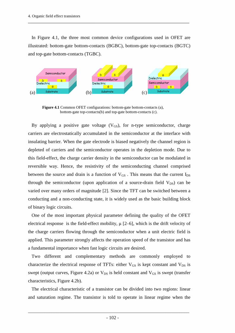
4. Organic field effect transistors ____________________________________________________________________
____________________________________________________________________ - 102 -
In Figure 4.1, the three most common device configurations used in OFET are
illustrated: bottom-gate bottom-contacts (BGBC), bottom-gate top-contacts (BGTC)
and top-gate bottom-contacts (TGBC).
(a)
Semiconductor
Substrate
G
SD
Dielectric
Semiconductor
Substrate
G
SD
Dielectric
(b)
Semiconductor
Substrate
G
Dielectric
D S
Semiconductor
Substrate
G
Dielectric
D S
(c) Substrate
SD
G
Dielectric
Semiconductor
Substrate
SD
G
Dielectric
Semiconductor
Figure 4.1 Common OFET configurations: bottom-gate bottom-contacts (a),
bottom-gate top-contacts(b) and top-gate bottom-contacts (c).
By applying a positive gate voltage (VGS), for n-type semiconductor, charge
carriers are electrostatically accumulated in the semiconductor at the interface with
insulating barrier. When the gate electrode is biased negatively the channel region is
depleted of carriers and the semiconductor operates in the depletion mode. Due to
this field-effect, the charge carrier density in the semiconductor can be modulated in
reversible way. Hence, the resistivity of the semiconducting channel comprised
between the source and drain is a function of VGS . This means that the current IDS
through the semiconductor (upon application of a source-drain field VDS) can be
varied over many orders of magnitude [2]. Since the TFT can be switched between a
conducting and a non-conducting state, it is widely used as the basic building block
of binary logic circuits.
One of the most important physical parameter defining the quality of the OFET
electrical response is the field-effect mobility, µ [2–6], which is the drift velocity of
the charge carriers flowing through the semiconductor when a unit electric field is
applied. This parameter strongly affects the operation speed of the transistor and has
a fundamental importance when fast logic circuits are desired.
Two different and complementary methods are commonly employed to
characterize the electrical response of TFTs: either VGS is kept constant and VDS is
swept (output curves, Figure 4.2a) or VDS is held constant and VGS is swept (transfer
characteristics, Figure 4.2b).
The electrical characteristic of a transistor can be divided into two regions: linear
and saturation regime. The transistor is told to operate in linear regime when the
4. Organic field effect transistors ____________________________________________________________________
____________________________________________________________________ - 103 -
drain (VDS) biases are much lower the gate (VDS) voltages. Instead, the saturation
regime takes place when VDS becomes higher than VGS. In the linear regime the
current flowing between drain and source through the channel follows the Ohm’s law
being proportional to the drain and gate voltages. As the VDS increases and
approaches the gate voltage, VDG drops to zero and the pinch-off of the channel
occurs. At this point the IDS becomes independent of the drain bias.
(a)
Linear regime Saturation regime Linear regime Saturation regime
(b) 0 VGSVTh0 VGSVTh
Figure 4.2 Plots of output curve (a) and transfer curve (b) for a n-type TFT.
Another important parameter is the threshold voltage (VTh), defined as the gate
voltage beyond which the conducting channel forms. A quasi-universal method used
in OFETs to extract this parameter consists of plotting the square root of the
saturation current as a function of the gate voltage (Figure 4.2b). The intercept of the
extrapolated linear curve with the gate-voltageaxis defines the threshold voltage.
In linear regime ( ThGSDS VVV −≤ ), IDS increases linearly with VDS and is described
by the following equation:
( )
−−=
2
2DS
DSThGSiDS
VVVV
L
WCI µ
(eq. 4.1)
where L is channel length, W is the channel width, Ci is the capacitance per unit
area of the insulating layer, VTh is the threshold voltage. The mobility can be
determined in linear regime from the transconductance:
DSi
tVGS
DSm V
L
WC
V
Ig
DS
µ=
∂∂=
=cos
(eq. 4.2)

4. Organic field effect transistors ____________________________________________________________________
____________________________________________________________________ - 104 -
by plotting IDS versus VGS at constant low VDS with VDS < ( VGS – VTh ) and
equating the value of the slope of this plot to gm.
For ThGSDS VVV −> , IDS tends to saturate (saturation regime) due to the pinch-off
the accumulation layer, and is modelled by the following equation:
( )2
2
1ThGSiDS VV
L
WCI −= µ
(eq. 4.3)
In the saturation regime, µ can be determined from the slope of the plot of DSI
vs. VGS. Although it is expected that mobility values extracted from linear and
saturation transfer-curves are very similar, this is not always the case for OFET[3].
Indeed, source and drain contact resistances (which are not taken into account in the
previous equations) can strongly influence the electrical behaviour of the organic
transistors.
The ratio of the current in the accumulation mode over the current in the depletion
mode is referred to as ION/IOFF. The ION/IOFF ratio measures the efficiency of the
device switch.
4.3 n4.3 n4.3 n4.3 n ----type O F E Ts based on type O F E Ts based on type O F E Ts based on type O F E Ts based on P erylene D iim ide P erylene D iim ide P erylene D iim ide P erylene D iim ide
derivativesderivativesderivativesderivatives
Organic Thin Film Transistors have received much attention for the fabrication of
low cost, flexible and large area electronic circuitry [7]. Both p-type and n-type
OFETs are required for the development of organic complementary metal oxide
semiconductor (CMOS) circuits [8–10], which are able to provide electronic
components with superior performances in terms of low static power consumption
and higher noise margins. Different from p-channel semiconductors which have been
widely studied for more than 20 years and exhibit excellent field-effect
characteristics [11,12], today n-channel semiconductors are less commonly
employed because of the low air stability and limited processing capability. Indeed,
despite many experimental works carried out over the past few years, nowadays the
number of n-channel compounds able to operate in ambient conditions with good
charge mobility (µ) remains very limited. Among them, Cyanated Perylene

4. Organic field effect transistors ____________________________________________________________________
____________________________________________________________________ - 105 -
Carboxylic Diimide derivatives are certainly the most promising n-channel
candidates owing to the high µ values (0.1 - 1 cm2/V s) [13,14], low sensitivity to
oxygen and moisture [15,16], remarkable environmental stability [17], good
solubility in common organic solvents such as toluene (TOL), chloroform (CF) and
o-dichlorobenzene (DCB). In particular, this last feature opens the way to the
fabrication of OFETs by direct printing methods, like the inkjet technology, which
are able to guarantee many advantages including low costs, low material wastage,
selective deposition of materials and non-contact patterning [18]. In electrically-
active organic devices, the semiconductor morphology plays a crucial role in
determining the final performances given the widely demonstrated correlation
between the crystalline microstructure of the organic layer and the corresponding
charge transport properties [19]. This issue is even more critical if the semiconductor
is deposited by inkjet printing, since the drop drying process drastically modifies the
morphology of the deposited material and can strongly affect also its overall
uniformity [20]. The poor uniformity of inkjet printed films is mainly caused by the
so called ‘coffee-stain’ effect. This phenomenon is ruled by the convective flow
occurring inside the sessile drop from its centre towards the edges, where the
evaporation rate is higher, for replenishing the evaporation losses [21]. As a
consequence, at the end of the drying process, the organic semiconductor results
largely localized at the rim of the printed droplet. A possible approach to reduce the
“coffee-stain” effect is based on the use of mixtures of solvents with different boiling
points and surface tensions. By mixing suitable high- and low-boiling point solvents,
indeed, temperature and surface tension gradients can be generated producing a
Marangoni flow from droplet rim to the centre [22–24]. This capillary flow balances
the ‘coffee-stain’ effect providing an appropriate spatial redistribution of the
material. In this way, morphology and uniformity of the printed films and, more in
general, the performances of the final devices can be improved by choosing the
appropriate component solvents, with particular care to their volatility and surface
tension properties, and their mixing ratio [23,24].

4. Organic field effect transistors ____________________________________________________________________
____________________________________________________________________ - 106 -
4.3.1 O F E Ts fabrication4.3.1 O F E Ts fabrication4.3.1 O F E Ts fabrication4.3.1 O F E Ts fabrication
In this thesis work, N,N’-bis(n-octyl)-1,6-dicyanoperylene-3,4:9,10-
bis(dicarboximide) (PDI-8CN2) films were deposited by inkjet printing on
Si(gate)/bare SiO2 (dielectric)/Au (contacts) substrates for the fabrication of n-
channel organic transistors. PDI-8CN2 is a molecule characterized by a rigid core ad
by the presence of cyanated groups which make it soluble (Figure 4.3).
Figure 4.3 Perylene PDI-8CN2 molecule. The circles inside the five core
hexagons indicate conjugated bonds with delocalized π orbitals.
Inkjet printed bottom-gate bottom-contact OFETs were fabricated on substrates
consisting of a 500 µm thick highly doped Silicon (Si++) layer, thin (200 nm) SiO2
dielectric barriers and pairs of interdigitated gold source-drain electrodes with 3-5 nm
of chromium employed as primer to improve the adhesion. The schema of the
structure of the transistor is reported in Figure 4.4a.
The active channels of the manufactured transistors have two possible lengths: L =
20 µm (Type I devices, FET3,4) and L = 40 µm (Type II devices, FET1,2) (Figure
4.4b). For all devices, however, the ratio between width (W) and length (L) of the
active channels is fixed at 550. Taking into account the size of the interdigitated
electrodes, the overall area printed was about 0.56 mm2 for Type I devices and 1.65
mm2 for Type II devices.

4. Organic field effect transistors ____________________________________________________________________
____________________________________________________________________ - 107 -
(a) Si n++
SiO2
AuAu
Cr
Si n++
SiO2
AuAu
Cr
(b) (c)
Figure 4.4(a) Schema of the OFET structure, (b) test pattern layout with source
and drain gold contacts and (c) magnification of the interdigitated electrode/channel structure.
Before printing of the semiconductor, the bare substrates were cleaned in sequence
in ultrasonic baths of acetone and isopropanol and dried with pure nitrogen (N2)
flow. PDI-8CN2 (Polyera ActivInk N1200, Polyera Corporation) was dissolved at 6
mg/mL concentration in mixtures of o-dichlorobenzene and chloroform at different
mixing volume ratios (DCB:CF 1:0, 4:1, 3:2, 1:4) in order to investigate the effect of
solvents and their mixtures on the printing quality. The possibility to use the single-
solvent system (0:1 DCB:CF) was not considered, since CF low boiling point
prevents to get the stable drop emission condition. The chosen solvents are the most
suitable to dissolve the semiconductor material and have right volatility and surface
tension properties for the inkjet printing processing (DCB: Tb = 180 °C, γ = 26.84
mN/m; CF: Tb = 61 °C, γ = 27.5 mN/m).
The prepared solutions were used as inks after filtering by means of a 0.2 µm
PTFE filter in order to remove possible agglomerates. The organic semiconductor
based inks were deposited by means of the inkjet equipment already described in the
chapter 1. The piezoelectric Drop on Demand (DoD) Microdrop printhead is
characterized by a 30 µm opening nozzle which corresponds to 20 pL droplet
volume. Moreover, the system allows to control the substrate temperature from the
ambient conditions (Tamb) up to 100 °C. Sequences of droplets were printed at 10 Hz
drop emission frequency and at printhead speed of 0.3 and 0.5 mm/s. During the
printing process, the substrate temperature was optimized for each mixing ratio in
order to prevent coalescence of the droplets printed on the target substrate.

4. Organic field effect transistors ____________________________________________________________________
____________________________________________________________________ - 108 -
4.3.2 M orphological characterization4.3.2 M orphological characterization4.3.2 M orphological characterization4.3.2 M orphological characterization
Morphological characterization were performed on the printed PDI-8CN2
semiconductor films in order to analyze the effects of the mixing ratio of the solvents
and printing parameters (drop overlapping degree, substrate temperature) on the film
quality.
In Figure 4.5 are reported the polarized optical microscopy images (Polyvar MET
Reichert-Jung) and the corresponding profilometric analyses (Tencor P10) of printed
PDI-8CN2 droplets.
This figure shows that the single-solvent system 1:0 DCB:CF generates an uneven
deposition of the material due to the “coffee-stain” effect. Hence, a ring like profile,
with lateral humps at the droplet rim and a thinner layer in the centre, is observed in
both the optical image (Figure 4.5a) and the corresponding 2D profile (Figure 4.5e).
Figure 4.5 Polarized optical images and corresponding 2D profiles of PDI-8CN2
drops on bare SiO2 substrates. The drops are inkjet printed by using DCB:CF mixtures at different volume mixing ratios and substrate temperatures: a,e) 1:0 @ T=90°C; b,f) 4:1 @ T=90°C; c,g) 3:2 @ T=90°C; d,h) 1:4 @ T=35°C.
On the other hand, by increasing the CF content, which has a lower boiling point
and a higher surface tension than DCB, an inward Marangoni flow was generated
during the droplet drying process in such a way to reduce the height of the humps at
the droplet rim. This phenomenon is clearly observable in the 2D profiles of the
investigated mixtures, as depicted in Figure 4.5f,g,h. In particular, Figure 4.5f

4. Organic field effect transistors ____________________________________________________________________
____________________________________________________________________ - 109 -
outlines how the CF presence reduces the ratio between the lateral hump height and
the height of the droplet centre. Moreover, it was found that the film uniformity can
be further improved if a suitable mixing ratio of the component solvents is
considered. Thus, the optical images and the related profilometric analyses reveal
that the best condition is achieved using 3:2 DCB:CF mixture (Figure 4.5c,g). At this
condition, the substrate region on which the single drop was printed appears fully
covered by the material, without the presence of empty zones. Finally, the further
increase of the CF content (1:4 DCB:CF, Figure 4.5d) leads to the formation of small
crystallites spread over the printed drop region and separated each other with marked
empty regions.
Organic thin film transistors were fabricated by inkjet printing PDI-8CN2 films on
Si++/SiO2 substrates with interdigitated gold source-drain electrodes. Films were
obtained by printing overlapped lines (50% overlapping degree), each one realized
by the sequence of overlapped drops. The lines were obtained with a drop
overlapping degree of 50% and 70%, nevertheless for all the mixing ratios the
optimal condition for forming uniform printed layers resulted 50%. The devices were
realized with all the analyzed mixing ratios in order to investigate the effect of the
drop overlapping on the printed film uniformity and, hence, on the performances of
the final transistors.
In Figure 4.6 the polarized optical images and the corresponding SEM (LEO 1530)
analyses of the printed PDI-8CN2 films are reported for each mixing ratio. For the
mixing ratios 1:0, 4:1 and 3:2 DCB:CF, where the contribution of the higher boiling
point solvent was greater, the substrate temperature was kept at 90 °C in order to
reduce the coalescence of the printed droplets. For 1:4 DCB:CF mixing ratio, where
the concentration of the lower boiling point solvent is higher, the substrate
temperature was optimized at T = 35 °C in order to avoid nozzle clogging that could
be thermally induced by higher temperatures for the proximity effect between the
printhead and substrate.
Despite the occurrence of the “coffee-stain” phenomenon for the printed single-
drops by using pure DCB as solvent (1:0 DCB:CF) (Figure 4.5a), the overlapping
effect induces the formation of an almost uniform film (Figure 4.6a). In this case, the
morphology of PDI-8CN2 film is characterized by the presence of large sized grains

4. Organic field effect transistors ____________________________________________________________________
____________________________________________________________________ - 110 -
induced by the slow crystallization process due to the DCB high boiling point,
similarly to the observed structure at the rim of the printed single-drop (Figure 4.5a).
On the contrary, as represented in Figure 4.6b,c,d, the increasing content of the lower
boiling point solvent causes the fast precipitation of PDI-8CN2 generating a more
and more pronounced concentration of smaller crystallite grains.
Figure 4.6 Polarized optical images and corresponding SEM analyses for PDI-
8CN2 films printed transverse to interdigitated fingers by different DCB:CF mixtures: (a,e) 1:0; (b,f) 4:1; (c,g) 3:2; (d,h) 1:4.
The results of the optical analysis were further supported by the SEM images
showing the presence of a large grain structure for the sample obtained by the single
solvent system (Figure 4.6e), a more uniform structure formed of larger grain
domains (average size 15 µm) intercalated with smaller crystallites (with average
size 2 µm), mostly oriented along the printing direction transverse to interdigitated
fingers, for the DCB:CF mixing ratio equal to 3:2 (Figure 4.6g), and, finally, an
uneven configuration with small crystallites alternated to empty regions for the 1:4
DCB:CF (Figure 4.6h). In the last case, a wide disorder of the crystallite orientation
is observed with a non uniform and random distribution with respect to the
interdigitated contacts. Moreover, for these devices, in order to take into account the
incomplete coverage of the active channels, the theoretical W/L ratios were corrected
after a careful inspection by the optical microscope.
A more detailed view of the film morphology in the regions where large and small
sized crystallites coexist is shown in Figure 4.7, in which are reported the atomic

4. Organic field effect transistors ____________________________________________________________________
____________________________________________________________________ - 111 -
force microscopy (AFM, XE100 Park instruments) for all the mixing ratio analyzed.
AFM characterization was carried out in non-contact mode amplitude modulation by
using a silicon nitride cantilever from Nanosensor.
The analysis of 30x30 µm2 AFM images showed that for the DCB:CF mixing
ratios of 1:0 and 3:2 (Figure 4.7a,c) the root mean square roughness (Rq) was about
100 nm with the presence of film regions characterized by the presence of peaked
zones with height up to 200 nm. For the optimized 3:2 DCB:CF mixture it is possible
to observe the presence of large crystallite (red dashed line in Figure 4.7c) where the
film surface appears flatter and the surface roughness is about 40 nm. The AFM
images for the 4:1 and 1:4 DCB:CF mixtures (Figure 4.7b,d) gave a higher roughness
value of about 150 nm due to the presence of peaked zone intercalated by disordered
crystallites. In particular, considering the mixture with higher presence of CF solvent
(which have the lower boiling point and surface tension properties) (Figure 4.7d), the
morphology was characterized by the presence of larger crystallite intercalated with
empty zones which could make the charge transport more difficult.

4. Organic field effect transistors ____________________________________________________________________
____________________________________________________________________ - 112 -
(a)
(b)
(c)
(d)
Figure 4.7 AFM images 30x30 µm2 and a magnification of 10x10 µm2 of printed PDI-8CN2 films employing mixing ration DCB:CF (a) 1:0; (b) 4:1; (c) 3:2 and (d) 1:4.

4. Organic field effect transistors ____________________________________________________________________
____________________________________________________________________ - 113 -
4.4.3 E lectrical characterization4.4.3 E lectrical characterization4.4.3 E lectrical characterization4.4.3 E lectrical characterization
The electrical response of the fabricated OFETs was investigated through the
output and transfer-curves. All electrical measurements were carried out in vacuum
(10-4 mbar) and in dark by using Janis Cryogenic Probe-Station system connected to
a Keithley 2612A Dual-Channel source-meter instrument.
Figure 4.8a shows the typical output-curves recorded for the inkjet printed PDI-
8CN2 transistors. These measurements refer to a device fabricated by the 3:2
DCB:CF mixture, however, the main qualitative features of these curves were found
common to all the analyzed devices independently from the solvent mixture. In
particular, the electrical response of all devices was characterized by the presence of
not negligible contact resistances (RC) between the source-drain electrodes and the
organic layer. This occurrence is specifically represented by the well evident sub-
linear behavior of the output curves in the low drain-source (VDS) voltage region. At
this stage, the physical origin of the contact resistances is not clear and further
experiments are required for the better understanding of this issue. It is likely,
however, that the main contribution to RC can be ascribed to the charge injection
process from the gold source electrode to the disordered semiconductor, which is
energetically characterized by a wide distribution of localized states close to the PDI-
8CN2 LUMO level.
On the other hand, the output curves (Figure 4.8a) reveal that the manufactured
transistors are able to carry significant currents (in the range of µA) even if no gate-
source (VGS) voltage is applied. This feature should be mainly related to the large
electron affinity of Cyanated Perylene derivatives which, interacting with the
chemical species (carbonyl and silanol groups) present on the SiO2 surface, give rise
to an unintentional doping process providing a significant density of free charge
carriers. In this way, these transistors can be considered as “normally on” and could
be operated both in accumulation and depletion modes.

4. Organic field effect transistors ____________________________________________________________________
____________________________________________________________________ - 114 -
Figure 4.8 Electrical response of inkjet printed PDI-8CN2 OFETs: a) 3:2 DCB:CF
output curves; b) transfer-curves in saturation regime (VDS = 50 V) of OFETs printed by employing different DCB:CF mixtures (in the inset the same curves are reported in semi-log scale).
In order to gain a straight comparison among the electrical performances of
transistors fabricated starting from different DCB:CF mixtures, the corresponding
transfer-curves measured in saturation regime (VDS = 50 V) are shown in Figure 4.8b.
These curves were recorded for Type I devices with L = 20 µm. The ability of the
devices to exhibit a significant conductance also in absence of VGS is further
confirmed by these measurements. The values of the onset voltage (Von), defined as
the voltage where the current IDS starts to increase in the semi-log plot, are in the
range between -30 V and -40 V (inset of Figure 4.8b). No clear correlation was found
between Von values and the composition of the solvent mixture.

4. Organic field effect transistors ____________________________________________________________________
____________________________________________________________________ - 115 -
Figure 4.9 Mobility values evaluated from the transfer-curves in the saturation
regime for inkjet printed PDI-8CN2 OFETs as a function of CF volume percentage in DCB: CF mixtures.
On the contrary, concerning both the maximum current and mobility values, the
best performances were found for transistors fabricated by 1:0 and 3:2 DCB:CF
mixtures. In particular, Figure 4.9 reports the plot of the mobility values, calculated
in the saturation regime by using the standard MOSFET equations, as function of the
chloroform percentage contained in the solvent mixing ratios. Mobility (µ) values are
given for both Type I (square symbols) and Type II (circle symbols) devices. This
analysis shows that for transistors with channel length L = 20 µm, the electrical
performances of 3:2 DCB:CF devices are similar (µ ~ 0.0035 cm2/V*s) to the single-
solvent samples obtained by employing pure DCB. These mobility values, much
lower than the maximum mobility values (about 0.1 cm2/V*s) reported in literature
for PDI-8CN2 transistors [13,14], can be attributable to both the transistor
configuration (bottom-gate bottom-contact) and the specific deposition process
(inkjet printing). In detail, it should be mentioned that PDI-8CN2 transistors
fabricated by evaporation on the same substrate type (Si/SiO2/Au) display maximum
mobility values ranging between 0.02 and 0.03 cm2/V*s [15]. Hence, the mobility
reduction by one order of magnitude, observed for the inkjet printed PDI-8CN2
active layers, can be ascribed solely to the specific characteristics of the deposition
method in good agreement with other results recently reported in literature (see in
particular ref. [14] and Table 1 therein).

4. Organic field effect transistors ____________________________________________________________________
____________________________________________________________________ - 116 -
Figure 4.9 also reveals that, when devices with L = 40 µm are considered, the 3:2
DCB:CF OFETs exhibit higher mobility values in comparison with the pure DCB
solvent devices. In particular, it is possible to point out that, even if the mobility
decrease between L= 40 µm and L= 20 µm devices is common to all the solvent
mixing ratios, the reduction factor is smaller than 2 when 3: 2 DCB:CF solvent
mixture is considered, while it exceeds 4 for the transistors deposited from the pure
DCB solvent. This finding seems to confirm that the solvent mixture approach, with
the optimized mixing ratio of 3:2 DCB:CF, is able to better ensure the film
uniformity and to limit the degradation of the device performances when larger
printed areas are considered. Finally, it can be noticed how, in agreement with the
optical analysis, the worst transistor performances were found for 1:4 DCB:CF
devices.
4.5 Sum m ary4.5 Sum m ary4.5 Sum m ary4.5 Sum m ary
In this fourth chapter of this thesis activity the fabrication of n-channel Cyanated
Perylene (PDI-8CN2) organic thin film transistors using the inkjet technique as
method for printing the semiconductor layers is performed. In order to improve the
uniformity of the printed films, an approach based on the employment of solvent
mixtures, with different boiling points and surface tensions, was followed. For each
mixture composition, the printing parameters, such as substrate temperature and drop
overlapping degree, were optimized to improve the reproducibility of the deposition
process and the structural quality of the final films.
The competing effect of the convective and inward Marangoni flows on the
crystalline microstructure of PDI-8CN2 was studied through morphological analyses
by means of polarized optical microscopy, scanning electron microscopy (SEM) and
atomic force microscopy (AFM).
The choice of an optimized ink composition was demonstrated to induce a specific
morphology of PDI-8CN2 films where larger grain domains are intercalated with
smaller crystallites mostly oriented along the printing direction. The analysis of the
electrical responses indicates that devices fabricated by the optimized solvent

4. Organic field effect transistors ____________________________________________________________________
____________________________________________________________________ - 117 -
mixture (3:2 DCB:CF) can retain good electrical performances even when the size of
the active channel is significantly increased. The analysis of the results showed that
the performances of the OFETs depends critically on understanding and controlling
the organic material’s molecular organization at interfaces gold/semiconductor.
These results confirm that the solvent mixture approach is an interesting route to
better address the uniformity issue in the inkjet printing technique applied to the
development of organic electronic circuitry.
4. Organic field effect transistors ____________________________________________________________________
____________________________________________________________________ - 118 -
B ibliography B ibliography B ibliography B ibliography [1] A. Tsumura, H. Koezuka, T. Ando, Macromolecular electronic device: Field-
effect transistor with a polythiophene thin film, Applied Physics Letters. 49 (1986) 1210.
[2] S.M. Sze, Physics of Semiconductor Devices, 2nd ed., Wiley-Interscience, 1981. [3] C.D. Dimitrakopoulos, D.J. Mascaro, Organic thin-film transistors: A review of
recent advances, IBM Journal of Research and Development. 45 (2001) 11-27. [4] G. Horowitz, R. Hajlaoui, R. Bourguiga, M. Hajlaoui, Theory of the organic
field-effect transistor, Synthetic Metals. 101 (1999) 401-404. [5] A.R. Brown, C.P. Jarrett, D.M. de Leeuw, M. Matters, Field-effect transistors
made from solution-processed organic semiconductors, Synthetic Metals. 88 (1997) 37-55.
[6] G. Horowitz, Organic Field-Effect Transistors, Advanced Materials. 10 (1998) 365-377.
[7] V. Subramanian, J.M.. Frechet, P.C. Chang, D.C. Huang, J.B. Lee, S.E. Molesa, et al., Progress Toward Development of All-Printed RFID Tags: Materials, Processes, and Devices, Proceedings of the IEEE. 93 (2005) 1330-1338.
[8] H. Klauk, U. Zschieschang, J. Pflaum, M. Halik, Ultralow-power organic complementary circuits, Nature. 445 (2007) 745-748.
[9] T.D. Anthopoulos, B. Singh, N. Marjanovic, N.S. Sariciftci, A. Montaigne Ramil, H. Sitter, et al., High performance n-channel organic field-effect transistors and ring oscillators based on C[sub 60] fullerene films, Appl. Phys. Lett. 89 (2006) 213504.
[10] F. Dinelli, R. Capelli, M.A. Loi, M. Murgia, M. Muccini, A. Facchetti, et al., HighMobility Ambipolar Transport in Organic LightEmitting Transistors, Advanced Materials. 18 (2006) 1416-1420.
[11] M. Mas-Torrent, M. Durkut, P. Hadley, X. Ribas, C. Rovira, High Mobility of Dithiophene-Tetrathiafulvalene Single-Crystal Organic Field Effect Transistors, Journal of the American Chemical Society. 126 (2004) 984-985.
[12] S. Allard, M. Forster, B. Souharce, H. Thiem, U. Scherf, Organic Semiconductors for Solution-Processable Field-Effect Transistors (OFETs), Angewandte Chemie International Edition. 47 (2008) 4070-4098.
[13] H. Yan, Z. Chen, Y. Zheng, C. Newman, J.R. Quinn, F. Dotz, et al., A high-mobility electron-transporting polymer for printed transistors, Nature. 457 (2009) 679-686.
[14] H. Yan, Y. Zheng, R. Blache, C. Newman, S. Lu, J. Woerle, et al., Solution Processed Top-Gate n-Channel Transistors and Complementary Circuits on Plastics Operating in Ambient Conditions, Advanced Materials. 20 (2008) 3393-3398.
[15] B.A. Jones, A. Facchetti, M.R. Wasielewski, T.J. Marks, Effects of Arylene Diimide Thin Film Growth Conditions on n-Channel OFET Performance, Advanced Functional Materials. 18 (2008) 1329-1339.
[16] M. Barra, F.V.D. Girolamo, F. Chiarella, M. Salluzzo, Z. Chen, A. Facchetti, et al., Transport Property and Charge Trap Comparison for N-Channel Perylene

4. Organic field effect transistors ____________________________________________________________________
____________________________________________________________________ - 119 -
Diimide Transistors with Different Air-Stability†, The Journal of Physical Chemistry C. 114 (2010) 20387-20393.
[17] A.S. Molinari, H. Alves, Z. Chen, A. Facchetti, A.F. Morpurgo, High Electron Mobility in Vacuum and Ambient for PDIF-CN2 Single-Crystal Transistors, Journal of the American Chemical Society. 131 (2009) 2462-2463.
[18] T. Kawase, T. Shimoda, C. Newsome, H. Sirringhaus, R.H. Friend, Inkjet printing of polymer thin film transistors, Thin Solid Films. 438-439 (2003) 279-287.
[19] K.-J. Baeg, D. Khim, J.-H. Kim, M. Kang, I.-K. You, D.-Y. Kim, et al., Improved performance uniformity of inkjet printed n-channel organic field-effect transistors and complementary inverters, Organic Electronics. 12 (2011) 634-640.
[20] F. Villani, P. Vacca, G. Nenna, O. Valentino, G. Burrasca, T. Fasolino, et al., Inkjet Printed Polymer Layer on Flexible Substrate for OLED Applications, The Journal of Physical Chemistry C. 113 (2009) 13398-13402.
[21] R.D. Deegan, O. Bakajin, T.F. Dupont, G. Huber, S.R. Nagel, T.A. Witten, Contact line deposits in an evaporating drop, Phys. Rev. E. 62 (2000) 756.
[22] H. Hu, R.G. Larson, Marangoni Effect Reverses Coffee-Ring Depositions, The Journal of Physical Chemistry B. 110 (2006) 7090-7094.
[23] J.A. Lim, W.H. Lee, H.S. Lee, J.H. Lee, Y.D. Park, K. Cho, Self Organization of Ink-jet Printed Triisopropylsilylethynyl Pentacene via Evaporation Induced Flows in a Drying Droplet, Advanced Functional Materials. 18 (2008) 229-234.
[24] D. Kim, S. Jeong, S.H. Lee, J. Moon, J.K. Song, Ink-jet printing of organic semiconductor for fabricating organic thin-film transistors: Film uniformity control by ink composition, Synthetic Metals. 159 (2009) 1381-1385.

5. Organic solar cells ____________________________________________________________________
____________________________________________________________________ - 120 -
CHAPTER 5
ORGANIC SOLAR CELLS
Recently, great interest has been devoted to cost-effective alternative energy
sources such as organic solar cells due to the low cost of fabrication, the mechanical
flexibility and the versatility of chemical structure from advances in organic
chemistry and ease of processing. As concerning this last point, the possibility of
organic materials processing by solutions at low temperatures makes them
employable for fabricating printed solar cells by using inkjet printing technology.
Polymer solar cells were manufactured by inkjet printing the regioregular poly(3-
hexylthiophene) (P3HT):[6,6]-phenyl-C61-butyric acid methyl ester (PCBM) blend
dissolved in pure solvents or solvent mixtures.
The influence of the chemico-physical properties of the solvents on the
morphology of the active layer was investigated through morphological and
electrical analyses.

5. Organic solar cells ____________________________________________________________________
____________________________________________________________________ - 121 -
5.15.15.15.1 Introduction of O PVIntroduction of O PVIntroduction of O PVIntroduction of O PV
For the past two hundred years, global economic growth has been fuelled almost
exclusively by conventional energy sources such as oil, coal and natural gas.
Unfortunately, this fossil fuels are finite energy sources that are rapidly depleting.
Moreover, greenhouse gas emissions from the use of fossil fuel have been widely
agreed as one of the major contributor to man-made climate change. Considering
these challenges, a more sustainable energy source is required as a long term solution
to the energy needs.
One of the most attractive method for the generation of electricity is based on the
photovoltaic (PV) technology. To date, silicon based-solar cells are the most
employed photovoltaic devices but, recently, interests are involving in polymer solar
cells (PSC) based on organic semiconductors. This class of materials permits to meet
the electricity demand as well as offer secondary benefits such as the extension of the
applications fields. In particular, this PSC can be used for laptop-recharging
briefcases, window tinting, put into tents, umbrellas, awnings and others.
The solubility of the organic semiconductor and the processability at low
temperatures allow their printability and, hence, the extension of the deposition
methods for fabrication of organic solar cells to printing technologies which
guarantee high production rate and low costs.
5.2 Photovoltaic w orking princip le5 .2 Photovoltaic w orking princip le5 .2 Photovoltaic w orking princip le5 .2 Photovoltaic w orking princip le
The photovoltaic effect was discovered in 1839 by Edmund Becquerel by using an
electrolytic cell made up of two metal electrodes. Becquerel observed that certain
materials produced small amounts of electric current when exposed to light. In 1905,
Einstein explained the photoelectric effect, which is the theoretical base for
understanding the photovoltaic effect. When photons illuminate a metal surface, free
electrons can escape from the metal surface due to excitation energy from the
incident light. In most cases, the absorbed photons pump ground state electrons to the

5. Organic solar cells ____________________________________________________________________
____________________________________________________________________ - 122 -
excited state. In photovoltaic devices, the excited electrons and the produced hole in
the ground state can be collected separately to produce power.
In order to convert sunlight into electricity, a solar cell devices should absorb as
much light as possible in the solar spectrum range (Figure 5.1).
Figure 5.1 AM0 and AM 1.5 solar spectra.
The organic photovoltaic process, schematically reported in Figure 5.2, is
composed of four steps: light absorption, charge generation, charge transport, and
charge collection [1].
The first step is the light absorption which depends on the bandgap energy (Eg) of
the semiconducting material and its intrinsic extinction coefficient. The second step
is the charge generation due to sunlight photons which bring the electrons from the
HOMO level (highest occupied molecular orbital) to excited state in the LUMO level
(lowest unoccupied molecular orbital). The excited electrons slightly relax and then
form an exciton, a bounded electron-hole pair. The exciton can diffuse inside the
organic semiconductor with a characteristic diffusion length of about 10-20 nm.
Because the exciton dissociation occurs only at the interface between the donor and
the acceptor, if excitons don’t reach the interface, they can recombine and the
absorbed energy is dissipated without generating photocurrent [2]. Therefore, in
order to realize a good organic solar cell an efficient dissociation of excitons is
needed. The third step is the charge transport process which involves the transport of
the dissociated charges towards the electrodes. During the charge pathways, if the
transporting medium has defects such as charge traps or barriers that hinder charge

5. Organic solar cells ____________________________________________________________________
____________________________________________________________________ - 123 -
transport, the cell performance decreases. Therefore, in order to increase the cell
performance it is necessary to optimize the transport process by reducing the losses.
The fourth step is the charge collection, which occurs when the transported charges
from the semiconductor to the cathode or anode are collected at the interface.
Figure 5.2 OPV working principle.
The electrical performance of an OPV cell is characterized by a current density-
voltage curve (J-V), schematically reported in Figure 5.3a.
(a) (b)
Figure 5.3 (a) Typical current density–voltage curve of an OPV solar cell and (b) schema
of the equivalent circuit of a solar cell.

5. Organic solar cells ____________________________________________________________________
____________________________________________________________________ - 124 -
The main parameters that quantitatively characterize the working of a OPV cell are
the short circuit current (Jsc), open circuit voltage (Voc), fill factor (FF), and power
conversion efficiency (PCE).
Figure 5.3a shows that the current-voltage product is negative and the cell
generates power when the voltage is between 0 and Voc. At V<0, the illuminated
device acts as a photodetector, consuming power to generate a photocurrent that is
light dependent but bias independent. At V>Voc, the device again consumes power.
This is the region where light emitting diodes operate.
The fill factor (FF) is defined as the ratio of the maximum obtainable power to the
product of the open circuit voltage and short circuit current:
OCSCVJ
VJFF maxmax=
(eq. 5.1)
With this, the power conversion efficiency (η) can be written as:
C
OCSC
Cin AE
VFFJ
AE
VJ
P
P
⋅=
⋅== maxmaxmaxη
(eq. 5.2)
where maxJ is the maximum current density, maxV is the maximum voltage, E is the
input light irradiance (in W/m2) and AC is the surface area of the solar cell.
In the real cell, power is dissipated through the resistance of the contacts and
through leakage currents. These effects are electrically equivalent to two parasitic
resistances placed in series (Rs) and in parallel (Rsh) as reported in Figure 5.3b. The
series resistance arises from the resistance of the cell material to current flow, mainly
through the front surface to the contacts. The parallel or shunt resistance arises from
leakage of current through the cell. Since series and shunt resistances reduce fill
factor, smaller Rs and larger Rsh values are required in order to fabricate an efficient
OPV cell.

5. Organic solar cells ____________________________________________________________________
____________________________________________________________________ - 125 -
5.3 O PV solar cells based on P3H T:PCB M blend5.3 O PV solar cells based on P3H T:PCB M blend5.3 O PV solar cells based on P3H T:PCB M blend5.3 O PV solar cells based on P3H T:PCB M blend
Polymer solar cells (PSC) are evolved as a promising cost-effective alternative to
silicon-based solar cells for their main advantages, such as low cost of fabrication,
very high speed and easiness of processing, mechanical flexibility and versatility of
chemical structure in organic chemistry [3–6].
Concerning the last item, the most exploited active material for photovoltaic
devices is the regioregular poly(3-hexylthiophene) (P3HT), p-type conjugated
polymer, blended with [6,6]-phenyl-C61-butyric acid methyl ester (PCBM), n-type
material [7,8] (Figure 5.4).
P3HT PCBM
Figure 5.4 Chemical structures of P3HT and PCBM.
The high efficiency and the solubility of this two materials in organic solvents, like
dichlorobenzene (DCB), chlorobenzene (CB) and chloroform (CF), allow the
employment of industrial deposition methods like inkjet printing for the fabrication
of large area organic solar cells. Among the various printing methods of functional
materials for PSC applications, the inkjet printing (IJP) technology is particularly
suited to realize patterned structures allowing an efficient use of the material, that
means a reduction of the waste products and the processing steps and, hence, a
reduction of the processing costs [5,9–13].
In organic solar cells, the active layer morphology plays a crucial role in
determining the final device performances because it strongly influences the charge
transport properties [14]. In particular, this issue is even more critical if the active
material is deposited by inkjet printing due to the “coffee-stain” effect that governs
the drop drying process [15]. This phenomenon determines an inhomogeneity of the

5. Organic solar cells ____________________________________________________________________
____________________________________________________________________ - 126 -
printed material that can be reduced by using mixtures of solvents with different
boiling points and surface tensions so that a Marangoni flow is generated [16–18].
Therefore, the right formulation and processing of the ink through the control of the
ink chemico-physical properties, the wetting of the ink/substrate system and the
definition of the printing parameters, are fundamental elements in organic solar cell
fabrication in order to improve the quality of the printed layers [11,15].
5.3.1 O PV fabrication5.3.1 O PV fabrication5.3.1 O PV fabrication5.3.1 O PV fabrication
In the present work, the influence of single solvents, 1,2-dichlorobenzene (DCB)
and chlorobenzene (CB), and their mixtures on the morphology and uniformity of
P3HT:PCBM films, which were deposited by inkjet printing on glass substrates for
the fabrication of polymer solar cells, was investigated. After optimizing the printing
parameters (printhead speed, drop emission frequency and substrate temperature), the
effect of the solvents on the morphology of P3HT:PCBM layer was analyzed through
optical microscopy, scanning electron microscopy (SEM) and profilometric analysis.
Organic photovoltaic cells were manufactured with ITO/PEDOT:PSS/
P3HT:PCBM/Ca/Al stack according to bulk heterojunction (BHJ) structure, currently
the most efficient architecture for polymer solar cells, where the active layer was
sandwiched between two electrodes with different work functions. The schematic of
the device stack is shown in Figure 5.5.
Figure 5.5 Schematic device structure of the manufactured polymer/fullerene bulk
heterojunction solar cell.

5. Organic solar cells ____________________________________________________________________
____________________________________________________________________ - 127 -
ITO-coated commercial coated glass was used as substrate. The employed ITO on
Corning®1737 glass (120 nm thick, sheet resistance < 15Ω/square) was cleaned
through standard process with detergent, subsequently with acetone and isopropanol
in ultrasonic bath, and, finally, drying in oven.
For PSC cell fabrication, ITO patterning was carried out through conventional
photolithography to define the front electrode geometry.
A 50 nm thick film of poly(3,4-ethylenedioxythiophene) (PEDOT) doped with
poly(styrenesulfonate) [(PEDOT:PSS), Baytron P HC Starck] was spin-coated from
a watery solution at 5000 rpm for 60 sec onto the substrates, after filtering through a
0.45 µm filter. The PEDOT:PSS films were then dried at 140 °C for 10 min under
nitrogen.
The active material, consisting of a blend of P3HT and PCBM, was then deposited
onto the hole transport layer (PEDOT:PSS) using the IJP technique. Regioregular
P3HT (Plextronics), electron donating material (p-type), and PCBM (Solenne BV),
electron accepting material (n-type), were used as received. The blend was prepared
by employing P3HT (6 mg/mL) and PCBM (4.8 mg/mL) with mixing ratio of 1:0.8
by weight and dissolving in two different single solvents, DCB (Tb = 180 °C, γ=
26.84 mN/m) and CB (Tb = 131 °C, γ = 33.4 mN/m), and in DCB:CB mixture at
volume mixing ratios 1:4, 1:1 and 4:1. The solvents DCB and CB were chosen
because they dissolve well the photoactive material and have right volatility and
surface tension properties for inkjet printing processing. All the solutions were
stirred on hotplate at 50 °C for 48 h.
The prints were carried out by means of the inkjet equipment already described in
the chapter 1 using Microdrop printhead with 30 µm opening nozzle. Solar cells with
34 mm2 active area were fabricated by printing the active material on the
PEDOT:PSS/ITO bottom electrode. The printing parameters were 5 Hz drop
emission frequency and 0.4 mm/s printhead speed with 50% overlapping degree. The
substrate temperature was optimized for each ink in order to prevent the coalescence
of the droplets printed on the target substrate and to reach the best film uniformity
condition.
The thickness of the P3HT:PCBM layer were analyzed by means of a surface
profilometer (KLA Tencor P-10 Surface Profiler). Optical micrograph, scanning

5. Organic solar cells ____________________________________________________________________
____________________________________________________________________ - 128 -
electronic microscopy (SEM, LEO 1530) and atomic force microscopy (AFM, Veeco
Nanoscope IV) analyses were carried out to investigate the morphology of the
printed films.
The devices were completed depositing Ca/Al top electrodes by thermal
evaporation in ultra-high vacuum (10-7 mbar) through shadow mask.
The devices were annealed on hotplate at 150 °C for 20 min in a nitrogen filled
glow box and then electrically characterized through external quantum efficiency
(EQE) and current-voltage (I-V) measurements performed under simulated AM 1.5G
illumination. I-V measurements were carried out by a Keithley 236 source measure
unit (Keithley Instruments Inc., Cleveland, USA) applying a voltage ramp rate of 10
mV/s from positive to negative potential. A Spectrosun® Solar Simulator (X25,
MARK II-Spectrolab USA) equipped with a AM1.5G filter was employed to provide
the simulated AM 1.5G white light illumination, whose intensity was calibrated with
an unfiltered mono-Si cell SC80 (certified by Fraunhofer ISE) for 1 sunlight intensity
of 100 mW/cm2. All the photovoltaic characterizations were performed in air at room
temperature.
5.3.2 M orphological characterization5.3.2 M orphological characterization5.3.2 M orphological characterization5.3.2 M orphological characterization
Optical micrograph images and the profilometric analyses of the printed
P3HT:PCBM films by dissolving the blend in pure CB and DCB solvents and
DCB:CB solvent mixtures are reported in Figure 5.6 and Figure 5.7, respectively.
Figure 5.6 Optical images and corresponding 2D-profiles of films of P3HT:PCBM dissolved in
(a, b) CB, (c, d) DCB.

5. Organic solar cells ____________________________________________________________________
____________________________________________________________________ - 129 -
200 µm200 µm
(b)
(a) (c)
(d)
200 µm200 µm200 µm200 µm200 µm
(b)
(a) (c)
(d)
Figure 5.7 Optical images and corresponding 2D-profiles of films of P3HT:PCBM dissolved in DCB:CB @ (a, b) 1:4, (c, d) 1:1 and (e,f) 4:1 mixing ratios.
For all the printed films, the analyses showed a morphology characterized by the
presence of the solute accumulation at the printed line edges. This effect is related to
the solute diffusion from the droplet centre towards the rim due to the higher
evaporation rate at the edge of the droplet. This phenomenon, known as “coffee-stain
effect”, induces an inhomogenity in the profile at the end of the drying process
clearly observable in the Figure 5.6b,d and Figure 5.7b,d,f. Although the chemico-
physical properties of each ink (vapour pressure, boiling, surface tension) induced a
different wetting of the ink-substrate system, the profile features were almost the
same for all the printed films obtained from different investigated solutions. This was
the result of the optimization of the printing parameters performed for each ink in
order to obtain continuous and uniform films.
The thicknesses of the printed films were estimated around 150 nm.
In Figure 5.8, the SEM analyses of the printed polymer:fullerene films are
reported. The images showed the typical surface profile previously observed both in
optical and profilometric analyses. Additionally, this analysis highlighted the
presence of some structures (circle in Figure 5.8d,e) preferentially close to the
printed line edges. These structures could be related to the phase demixing at the film
surface.

5. Organic solar cells ____________________________________________________________________
____________________________________________________________________ - 130 -
(c) (d) (e)(c) (d) (e)
Figure 5.8 SEM images of the inkjet printed films of P3HT:PCBM dissolved in (a) CB, (b)
DCB, and DCB:CB @ (c) 1:4, (d) 1:1, (e) 4:1 mixing ratios.
In order to investigate the influence of the quality of the active material films on
the solar cells performances, the devices were completed with Ca/Al cathode and
characterized immediately after the annealing process.
5.3.3 E lectrical characterization5.3.3 E lectrical characterization5.3.3 E lectrical characterization5.3.3 E lectrical characterization
The current density versus voltage (J-V) curves for the manufactured solar cell by
using pure solvents and the DCB:CB 4:1, are shown in Figure 5.9.
Figure 5.9 J-V light curves for photovoltaic devices realized by inkjet printing a blend of
P3HT:PCBM dissolved in CB (circle), DCB (square) and DCB:CB (4:1) (star).

5. Organic solar cells ____________________________________________________________________
____________________________________________________________________ - 131 -
The corresponding parameters extracted from J-V curves for all the investigated
devices, such as Voc, Jsc, fill factor (FF) and power conversion efficiency (η) of the
devices are summarized in Table 5.1.
Solvent ηηηη [%] FF[%] J SC [mA/cm2] VOC [mV] CB 1.0 28 6.1 594 DCB 0.3 20 3.5 412 DCB:CB 1:4 1.2 35 7.5 465 DCB:CB 1:1 2.2 53 7.1 568 DCB:CB 4:1 2.4 51 8.0 602
Table 5.1 Summary of the characteristics of the photovoltaic devices showing the power conversion
efficiency (η),the fill factor FF, the short circuit current JSC and the open circuit voltage VOC .
The electrical analysis showed that the use of the solvent mixture strongly
enhances the device performances. This can be attributed to the improvement of the
homogeneity of the active material film as previously observed and also to a suitable
phase separation induced from the solvent mixture.
In particular, on the solar cell realized by using DCB:CB 4:1 which showed the
best electrical performances, AFM analysis was performed (Figure 5.10).
Figure 5.10 AFM images (topography (left) and phase(right)) of the P3HT:PCBM blend
printed by using DCB:CB 4:1 as solvent mixture.
The results of this analysis showed that for the optimized mixing ratio the
morphology of the printed active layer is almost uniform with a clear phase
separation between P3HT and PCBM. This phase separation is characterized by
domains with average size of about 20 nm. This is a result of polymer self
organization that leads to an increase in device power conversion efficiency.

5. Organic solar cells ____________________________________________________________________
____________________________________________________________________ - 132 -
5.4 Sum m ary5.4 Sum m ary5.4 Sum m ary5.4 Sum m ary
In this fifth chapter the fabrication of P3HT:PCBM based solar cells using the
inkjet printing technique as method for depositing the active material layer is
reported. In order to improve the uniformity of the printed films, an approach based
on the employment of solvent mixtures, with different boiling points and surface
tensions, was followed. The best polymer solar cell realized by using a DCB:CB 4:1
volume mixing ratio has a power conversion efficiency of 2.4%. This higher
electrical performance can be attributed to an improved film uniformity and
morphology. Indeed, the analyses showed that the active material is characterized by
a clear phase separation between the P3HT and PCBM (the donor and the acceptor,
respectively) thanks to an optimized polymer organization which induces an higher
conversion efficiency.

5. Organic solar cells ____________________________________________________________________
____________________________________________________________________ - 133 -
B ibliographyB ibliographyB ibliographyB ibliography [1] S.R. Forrest, The Limits to Organic Photovoltaic Cell Efficiency, MRS Bulletin.
30 (2005) 28-32. [2] M. Knupfer, Exciton binding energies in organic semiconductors, Applied
Physics A: Materials Science & Processing. 77 (2003) 623-626. [3] C.J. Brabec, V. Dyakonov, J. Parisi, N.S. Sariciftci, Organic Photovoltaics:
Concepts and Realization, 1st ed., Springer, 2003. [4] S. Günes, H. Neugebauer, N.S. Sariciftci, Conjugated polymer-based organic
solar cells, Chem. Rev. 107 (2007) 1324-1338. [5] F.C. Krebs, J. Fyenbo, M. Jørgensen, Product integration of compact roll-to-roll
processed polymer solar cell modules: methods and manufacture using flexographic printing, slot-die coating and rotary screen printing, J. Mater. Chem. 20 (2010) 8994-9001.
[6] H. Hoppe, N.S. Sariciftci, Organic Solar Cells: An Overview, Journal of Materials Research. 19 (2004) 1924-1945.
[7] W. Ma, C. Yang, X. Gong, K. Lee, A.J. Heeger, Thermally Stable, Efficient Polymer Solar Cells with Nanoscale Control of the Interpenetrating Network Morphology, Advanced Functional Materials. 15 (2005) 1617-1622.
[8] Hwajeong Kim, Minjung Shin, Jiho Park, Youngkyoo Kim, Effect of Long Time Annealing and Incident Light Intensity on the Performance of Polymer: Fullerene Solar Cells, IEEE Transactions on Nanotechnology. 9 (2010) 400-406.
[9] C.N. Hoth, S. a Choulis, P. Schilinsky, C.J. Brabec, High Photovoltaic Performance of Inkjet Printed Polymer:Fullerene Blends, Advanced Materials. 19 (2007) 3973-3978.
[10] N. Moldovan, R. Picos, E. Garcia-Moreno, Parameter Extraction of a Solar Cell Compact Model usign Genetic Algorithms, in: Spanish Conference on Electron Devices, 2009. CDE 2009, IEEE, 2009: pagg. 379-382.
[11] T. Aernouts, T. Aleksandrov, C. Girotto, J. Genoe, J. Poortmans, Polymer based organic solar cells using ink-jet printed active layers, Applied Physics Letters. 92 (2008) 033306.
[12] Lange, A., A new approach to the solvent system for inkjet-printed P3HT:PCBM solar cells and its use in devices with printed passive and active layers, Solar energy materials and solar cells. 94 (2010) 1816-1821.
[13] S.H. Eom, H. Park, S.H. Mujawar, S.C. Yoon, S.-S. Kim, S.-I. Na, et al., High efficiency polymer solar cells via sequential inkjet-printing of PEDOT:PSS and P3HT:PCBM inks with additives, Organic Electronics. 11 (2010) 1516-1522.
[14] J. Liu, Y. Shi, Y. Yang, Solvation-Induced Morphology Effects on the Performance of Polymer-Based Photovoltaic Devices, Advanced Functional Materials. 11 (2001) 420-424.
[15] R.D. Deegan, O. Bakajin, T.F. Dupont, G. Huber, S.R. Nagel, T.A. Witten, Capillary flow as the cause of ring stains from dried liquid drops, Nature. 389 (1997) 827-829.
[16] H. Hu, R.G. Larson, Marangoni Effect Reverses Coffee-Ring Depositions, The Journal of Physical Chemistry B. 110 (2006) 7090-7094.

5. Organic solar cells ____________________________________________________________________
____________________________________________________________________ - 134 -
[17] J.A. Lim, W.H. Lee, H.S. Lee, J.H. Lee, Y.D. Park, K. Cho, SelfOrganization of Ink-jet-Printed Triisopropylsilylethynyl Pentacene via EvaporationInduced Flows in a Drying Droplet, Advanced Functional Materials. 18 (2008) 229-234.
[18] D. Kim, S. Jeong, S.H. Lee, J. Moon, J.K. Song, Ink-jet printing of organic semiconductor for fabricating organic thin-film transistors: Film uniformity control by ink composition, Synthetic Metals. 159 (2009) 1381-1385.

Conclusions ____________________________________________________________________
____________________________________________________________________ - 135 -
CONCLUSIONS
The present thesis work concerns the realization and characterization of organic
electronic devices fabricated by means of inkjet printing technique. The experimental
results pointed out that the characteristics of this technology makes it versatile for the
manufacturing of different devices like sensors, field effect transistors, solar cells and
optical structures.
The focus of this research is the feasibility study on the control of the morphology
and the uniformity of printed materials acting on the ink chemico-physical
parameters (solvent composition, viscosity), on printing parameters (substrate
temperature, drop emission frequency, drop overlapping degree, number of the
overlapped layers) and on substrate properties (wetting, surface energy, roughness).
The methodology for optimizing the working parameters is studied for each
manufactured device since these parameters act in different way on the various
ink/substrate systems. The right combination of these parameters allows to obtain the
more appropriate morphology for each application, sometimes inducing also
microstructural modifications, which are the main responsible of the final device
working.
For the realization of the sensor devices, a polymer nanocomposite (PNC) was
used as sensing material for fabricating VOCs (volatile organic compounds)
chemiresistive sensors. The polystyrene (PS)/carbon black (CB) based ink was
printed on different substrates, non-flexible (alumina, glass) and flexible (PET
(polyethylene terephthalate), glossy paper). By depositing one or more lines of PNC
based ink, differently orientated with respect to the fingers of the interdigitated
electrodes, the relation between the sensing material geometry and the device
Conclusions ____________________________________________________________________
____________________________________________________________________ - 136 -
performances was studied. The results pointed out that the PNC based chemical
sensors fabricated by IJ printing lines ‘transverse’ to the transducer fingers showed
the best electrical performances when exposed to organic vapours. This optimized
configuration was used for studying the effect of the substrate morphology on the
printed film quality and, hence, on the device performances. The substrates
employed were glass, PET and glossy paper and they were used untreated and after
plasma treatments (O2, CF4). The optimized condition to obtain a continuous and
uniform deposition of the sensing material was reached by CF4 surface treatment. By
combining this condition with the optimization of geometry and thickness of the
printed layer, it was possible to improve the sensing material morphology and, hence,
to enhance the sensor performances. All the sensors realized showed good electrical
responses to acetone and ethanol vapours. In particular, the sensors inkjet printed on
glossy paper showed the best electrical responses to the different analytes opening
new perspectives for food distribution, electronics and textile industry applications.
The study developed in the sensor field highlighted the peculiarity of this innovative
technology in performing patterns which are exclusive of this deposition method and
which allow to realize optimized architectures for enhancing the device
performances. Moreover, the analysis on the surface treatments pointed out that the
chemico-physical properties of the substrate have a key role in printing process since
these parameters control the wetting and so the right adhesion of the sensing
material.
The research activity related to the optical applications was focused on the
realization of microlenses by additive deposition of a optical grade polymer material
and on the structuring of polymer layers by means of inkjet etching (IJE), an
application of IJP technology. The IJE technique consists in depositing drops of
solvents or solvent mixtures onto a soluble polymer layer, inducing the local
dissolution of the polymer with a final redistribution whose shape depends on the
surface tension properties of the solvent mixtures. Concave- and convex- shaped
microstructures were realized by using single solvents (N-Methyl-2-pyrrolidone
(NMP), toluene (TOL)) and solvent mixture (TOL:NMP), respectively. The effects
of the substrate temperature and the number of the printed droplets on the
geometrical parameters of the microstructures were investigated. As application, the

Conclusions ____________________________________________________________________
____________________________________________________________________ - 137 -
concave-shaped structures were employed as texturing of polymer under-layer of
OLED devices in order to destroy the interference effects observable in the device
emission spectrum. The convex-shaped microstructures were used as microlenses
coupled to OLED devices in order to improve the OLED out-coupling efficiency.
Concerning the optical structures realized by additive deposition, microlenses were
fabricated by inkjet printing drops of PMMA (Poly(methyl methacrylate)) dissolved
in different solvents (toluene -TOL-, N-Methyl-2-pyrrolidone -NMP-, chlorobenzene
-CB-, ortho-dichlorobenzene -DCB-) and their mixtures (NMP:TOL, CB:NMP,
CB:DCB, DCB:TOL, NMP:DCB). The substrate was glass covered by a transparent
hydrophobic film with the aim to freeze the printed droplet. During the printing, the
substrate temperature was kept at 17 °C in order to increase the drying time so
improving the microstructure quality. The effects of the ink viscosity and solvents on
the optical quality of the structures were investigated by profilometric and optical
analyses. In particular, the results pointed out that the surface tensions properties of
the solvents and the viscosity of the solutions are main responsibles of the shape and
of the spherical symmetry of the microlenses. The optical properties of such
microlenses were analyzed through a Mach–Zehnder interferometer in confocal
configuration. This analysis allowed to evaluate the wave aberrations of the realized
microlenses with respect to an ideal spherical shape and the results demonstrated that
the right choice of the solvent and the polymer concentration in preparing the ink can
enhance the optical quality of the microlenses. The activity related to optical
application pointed out that the chemico-physical ink properties, which can suitably
modified by formulating the ink by means of the right solvents, strongly influences
the optical quality of microstructures manufactured by highly reproducible
deposition method.
The research activity about OFETs was focused on the formulation and processing
of a n-type semiconductor material based on Cyanated Perylene Carboxylic Diimide
derivative, soluble in organic solvents and with good electrical properties and air
stability. This study pertained the definition of the ink chemico-physical properties
combined with the printing parameters in order to improve the quality of the printed
layer. Films of N,N’-bis(n-octyl)-1,6-dicyanoperylene-3,4:9,10-bis(dicarboximide)
(PDI-8CN2) were printed by solution prepared with different solvent mixtures

Conclusions ____________________________________________________________________
____________________________________________________________________ - 138 -
(dichlorobenzene (DCB), chloroform (CF)) on Si (gate)/bare SiO2 (dielectric)/Au
(contacts) substrates for the fabrication of n-channel organic transistors. For each
mixture composition the printing parameters, such as substrate temperature and drop
overlapping degree, were optimized to define the reproducibility condition of the
deposition process and to improve the structural quality of the films. Morphological
analyses were performed by means of polarized optical microscopy, scanning
electron microscopy (SEM) and atomic force microscopy (AFM). The identification
of the optimized ink composition was demonstrated to induce a specific morphology
of PDI-8CN2 films where larger grain domains are intercalated with smaller
crystallites mostly oriented along the printing direction. The analysis of the electrical
responses indicated that the devices fabricated by the optimized solvent mixture of
DCB:CF have higher electrical performances, depending on the improved molecular
organization at the interfaces between gold and the organic semiconductor.
The research activity related to the OPV was focused on the realization of solar
cells by printing P3HT:PCBM blend as active material. The study was focused on
the optimization of the device performances by employing different solvents and
solvent mixtures to dissolve the blend. The effects of the working parameters on the
electrical performances of devices were investigated by means of optical and
morphological analyses. The results indicated that the employment of the right
solvent mixture greatly influence the film morphology and the solar cell
performances. Such behaviour was due to optimum phase separation of the two blend
components, improved light absorption properties and reduced recombination losses
that are attributed to an improved morphology and charge transport. Both OFET and
OPV activities highlighted that the control of the ink and printing parameters is
crucial for the morphological and, mainly, structured quality of the printed active
material.

____________________________________________________________________ - 139 -
ACKNOWLEDGEMENT
“The time you spend on helping others is time gained”….
…“Il tempo che usi per aiutare gli altri è tempo guadagnato”. Così recita un
bigliettino dei baci perugina (e chi mi conosce sa che è proprio nel mio stile
cominciare così!). Ed è questo motivo che mi spinge a scrivere i ringraziamenti: per
dire GRAZIE a tutti quelli che hanno speso il loro tempo per aiutarmi e farmi
crescere… non è stato tempo perso ma tempo guadagnato!
Il primo grazie va ovviamente a Carla che mi ha permesso di passare questi 3 anni
in ENEA e che ho imparato in questi anni ad apprezzare per la sua bontà.
Un MEGA ringraziamento va a Fulvia che mi ha seguito e guidato per tutti questi
anni, facendomi crescere sia professionalmente che personalmente. So di non
sbagliarmi quando dico che è una delle persone più forti, intraprendenti e affettuose
che io conosca. Grazie di cuore!
Un grande ringraziamento va anche ad Antonio C. che mi ha seguito come mio
tutor in questo “viaggio” durato 3 anni.
E come dimenticare il mitico Mario B. Grazie per tutti i tuoi consigli e spiegazioni.
Ho imparato veramente tanto grazie a te!TNK.
E un grazie va a Fausta, una persone più buone e “felici” che abbia mai conosciuto,
grazie dell’aiuto, delle chiacchierate e della compagnia nei viaggi in treno. TVB
E grazie anche ad Anna e Peppe Nenna, che mi hanno sopportato in questi anni,
sempre pronti ad aiutarmi in tutte le mie richieste. Lo so che a volte sono stata
insopportabile e perciò vi meritate un SUPER-MEGA GRAZIE!
Grazie di tutto cuore al mio gigante buono Peppe P., una delle persone più
volenterose, intraprendenti e soprattutto buone che conosco. Grazie di tutto!
Un grazie al mio compagno di “bis colazione!”, Peppe. Grazie dei tuoi consigli e
delle chiacchierate in cima alle scale che mi hanno fatto capire molte cose!

Aknowledgement ____________________________________________________________________
____________________________________________________________________ - 140 -
Un grande grazie va a Pasquale e Rosita. Lavorare con voi mi ha permesso di
apprezzare la vostra passione per il lavoro e mi ha spronato ad impegnarmi sempre di
più. Grazieeee!!
E poi come dimenticare Antonio I., sempre disposto ad aiutarmi ad ogni mia
richiesta. Grazie della disponibilità e dell’amicizia. Sei un grande!
Un grazie a Emilia che, anche se per poco, ha condiviso le gioie e i dolori della
convivenza di ufficio! Grazie della tua amicizia, infinita pazienza e dei tuoi consigli!
Un grazie va a Dante, Matteo, Michele, Ciro e a tutti quelli del “Centro di calcolo”
che mi hanno potuto apprezzare i miei “Karaoke live” post pranzo anti abbiocco!
“anima mia” è per voi!
Grazie anche ad Antonio D.G. per la sua collaborazione e la sua pazienza. Spero di
non essere entrata nella tua lista nera in così poco tempo! Hihi
E grazie di cuore a Aneesh, Romina, Tommaso, Vera, Ettore, Tiziana, Paola per
tutto l’aiuto, la pazienza e… ….i dolci che mi avete offerto!!!
E poi grazie ancora a tutti coloro che hanno condiviso i “lunghi viaggi verso casa”:
Antonio, Carla, Franco, Grazia, Raffaele, Franco R., Giuseppe F., Danilo, Antonella,
Gianni, e tutti coloro che per colpa dei miei poveri neuroni ho dimenticato.
E grazie devo dirlo anche alle mie amiche Laura, Tina, Katia, Mariateresa,
Annarita, Giovanna ed Annapaola per le infinite chiacchierate ed uscite insieme.
E infine una SUPER-MEGA-GIGA ringraziamento va a Emanuele che in questi
anni mi ha veramente sopportato e supportato in ogni momento. Il mio vero angelo
sei tu.

____________________________________________________________________ - 141 -
GLOSSARY
Symbol Full expression Unit L atin lettersL atin lettersL atin lettersL atin letters
d Nozzle diameter m E Energy eV f Frequency s-1 h Height m L Channel Length m n Refractive index - Mw Molecular Mass - R Resistance Ω Re Reynolds number - SE Surface Energy mN m-1 T Temperature °C Tb Boiling temperature °C V Tension V W Channel width m We Weber number - Z Fromm number -
G reek lettersG reek lettersG reek lettersG reek letters
η Viscosity Pa s η Power conversion efficincy µ Mobility cm2 V-1 s-1 γ Surface tension N m-1 θ Contact angle ° ρ Density Kg m-3 τ Shear stress Pa •γ
Shear rate s-1
A bbreviationsA bbreviationsA bbreviationsA bbreviations
AFM Atomic Force Microscopy Au Gold BE Bottom Emitting BHJ Bulk heterojunction CB Chlorobenzene CB Carbon black CF Chloroform

Glossary ____________________________________________________________________
____________________________________________________________________ - 142 -
CF4 Carbon tetrafluoromethane plasma
Cr Chromium CIJ Continuous Inkjte DCB Dichlorobenzene DLS Dynamic Laser Scattering DoD Drop on Demand EL Electroluminescence HOMO Highest occupied molecular orbital IJE Inkjet etching IJP Inkjet printing LoD Limit-of-detection LUMO Lowest unoccupied molecular orbital NMP N-Methyl Pirrolidone O2 Oxygen plasma OFET Organic Field Effect Transistor OLED Organic Light Emitting Diode OPD Optical path difference OPV Organic photovoltaic P3HT poly(3-hexylthiophene) PCBM [6,6]-phenyl-C61-butyric acid methyl ester PDI Polydispersity index PDI-8CN2 n-type organic semiconductor PEDOT:PSS Poly(3,4-ethylenedioxythiophene):poly(styrenesulfonate) PET Polyethylene terephthalate PI Polyimmide PMMA Polymethyl methacrylate PNC Polymer Nanocomposite ppm Parts per million PS Polystyrene PSC Polymer solar cell P-V peak-to-valley RMS root-mean-square RF Radio Frequency SEM Scanning Electron Microscopy Si Silicon SiO2 Silicon Oxide Si3N4 Silicon Nitride TE Top Emitting TEOS/PFTEOS Hydrophobic layer TOL Toluene VOC Volatile Organic Compounds VRH Variable Range Hopping Theory ZnO Zinc Oxide