readout no.14 13 selected article - · pdf fileendpoint monitor on manufacturing process in...
TRANSCRIPT

Se
le
ct
ed
A
rt
ic
le
English Edition No.14 February 201162
Selected Article
Applications of Plasma Emission Endpoint Monitor EV140C
Hiroshi Iida
The Optical Emission Spectroscopy (OES) is major monitoring principle for detecting the process endpoint from signal trend changing of plasma emission in the process chamber of semiconductor manufacturing. The endpoint detection capability is improved by a CCD spectrograph which is able to use the wide range optical spectrum. But the CCD spectrograph brings difficulty of the analyzing operation to build the process endpoint condition due to huge data volume of wide range spectrum. And process users request also the capability of training a lot of data from manufacturing process. We explain about a practical example of the plasma emission endpoint monitor on manufacturing process in this article.
Introduction
During designing semiconductor devices improvement, especially the dry etching patterning technology is taken into account as an important technology in semiconductor manufacturing processes. This dry etching patterning technology is applied in other industry also, a f lat-panel display, MEMS and an optical device, and so on.Plasma emission in the process chamber has various information. Therefore OES technique has been used in various fields of the process development and the process management on production. Process engineers improve dry etching process technologies and OES analysis techniques together. And they require also more efficient engineering tools which improve the productivity.We describe a practical example of the plasma emission endpoint monitor on manufacturing process in this article.
Subject
A measurement principle of plasma emission endpoint detection is indicated in Figure 1. Much plasma emission from radicals, ions of process gases, an estrangement ion from an etching target film, and byproduct of reaction are observed in the process chamber. The status of plasma emission during wafer processing is monitored by wideband multi-channel CCD spectrograph through an optical fiber from a chamber view port. We attempt the
case of end point detection of the silicon dioxide layer etching process. When the etching proceeds and reaches the boundary of the target layer, plasma emission based on CFx of etching gas increase, and the one based on CO of reaction by-product decrease. These variations of plasma emission can be defined as a process endpoint when acquiring signals reaches threshold.
Process time (sec)
Pla
sma
Inte
nse
(a.u
.)
BeforeInterface
DuringInterfaceEtching
OverEtching
Ions of etching gases
Reactive elements from etching layer
Reactive elements from substrate
Figure 1 Etching progress and signal variation in plasma emission
There are three important features of an OES endpoint monitor as follows.- Easy wavelength selecting capability of plasma emission
of radicals or ions for the process endpoint- Real time capability of calibration processing and
endpoint detection with manufacturing tool- Validation suppor t to build the reliable endpoint
detecting condition before release to a production line

English Edition No.14 February 2011
Technical Reports
63
In addition, there are many application requests that are the real time process quality controls with detections of defects, a process chamber status monitoring from information of plasma emission, and others.The confirming of these detecting conditions with actual manufacturing process data is important thing. Process engineer should evaluate the results whether the optimized endpoint condition can be released in actual device production.
We developed the real time endpoint detection system that is adopted for many requests from process engineers. The software supports engineering works to build the new endpoint detecting condition systematically with easy operation, and to introduce this new condition into manufacturing process smoothly.
EV-140C The Product Specification.
OES endpoint monitor EV-140C consists of the small sensor unit, which is integrated into process tool, and the controller unit. It has the back thin type CCD device in a 200-800 nm wavelength range spectrograph that has high S/N ratio in the whole spectrum. It allows a fast sampling of spectrum data and transfer by an Ethernet access between the sensor and the controller unit.
Table 1 The main product specification
Item SpecificationProduct Name Plasma Diagnosis Endpoint MonitorModel Name EV-140CSensor unitRange of wavelength 200-800 nmOptical resolution Under 2.0 nm @λ=200-500 nm
Under 2.5 nm @λ=500-700 nm (FWHM theoretical resolution)
Optical bench unit design Polychromator of flat field aberrationCCD sensor Back thin type CCD liner image sensorA/D resolution 16 bitExposure time 20 ms~2.5 sExternal control
Optical fiberquartz fiber : 7 pcs. of 230 μm Core, Effective diameter : 690 μm
Remote communication Parallel I/O / RS232C serial protocolSignal output - Parallel I/O port
- Analog output 2ch 0-5 VDC
Sensor unit size142×257×152 mm (W×D×H DC power type)
Mass 4.0 kg (DC power type)
The real time monitoring platform; Sigma-P software is installed in the controller unit. The software extracts effective wavelength signals of endpoint detection automatically, and then the wavelength signals are transferred to time trend data. Process engineer modifies the time trend data with filter or signals enhancement, and then he sets the evaluation and endpoint condition by logical expression formula. The software has operability
user interface for building the measurement recipe to realize an efficiently engineering work.
It has a several remote control capability with a parallel IO, a RS232C or an Ethernet to communicate with process tool. The measurement signal of the specified wavelength or calculated data can be output in real time by 2 channel analog signal or serial communication. For example, this signal data is useful for control of the process pressure or the flow rate on the production equipment.SQL database supports search function from huge volume data on manufacturing process or statistic data for process optimizations. Additionally there are many useful features that suppor t engineering task to optimize parameters using the multi-run comparison and statistic data from manufacturing data.Our software offers the Rupture Intensity algorithm for data processing instead of general PCA (Principal Components Analysis) technique.This algorithm can find the starting point of variation by liner fitting to time trend curves that is specified by data of calculations window. The Rupture Intensity value is calculated from the angle formed by two fitted line and the number of data of 2 sections. This value provides smoothed curves without any data delay by the algorithm, even the case of small and noisy signal variation at the boundary of etching stop interface.
Process Engineering Work of OES Endpoint Condition
Figure 2 shows general process engineering flows using a n OE S e n d p o i n t m o n i t o r i n a s e m ic o n d u c t o r manufacturing site. OES technique is used at the various phases in a test production, an improvement process and a
Selected Article
Applications of Plasma Emission Endpoint Monitor EV140C
Hiroshi Iida
The Optical Emission Spectroscopy (OES) is major monitoring principle for detecting the process endpoint from signal trend changing of plasma emission in the process chamber of semiconductor manufacturing. The endpoint detection capability is improved by a CCD spectrograph which is able to use the wide range optical spectrum. But the CCD spectrograph brings difficulty of the analyzing operation to build the process endpoint condition due to huge data volume of wide range spectrum. And process users request also the capability of training a lot of data from manufacturing process. We explain about a practical example of the plasma emission endpoint monitor on manufacturing process in this article.
Production control phase
Test production phase
• Evaluation of plasma emission:• Process test:
- Process endpoint monitor- Plasma condition monitor- Chamber cleaning monitor
• Improvement and optimization:- Process endpoint monitor- Process defect monitor
• Quality control:- Uniformity etching process- Unstable plasma emission
①
②
③
Figure 2 Practical example of engineering flow
Se
le
ct
ed
A
rt
ic
le
English Edition No.14 February 201164
Selected Article Applications of Plasma Emission Endpoint Monitor EV140C
mass production phase. Because observed plasma emission in process chamber has so many chemical/ physical information.
(1) Making end Point Condition on Process Development Phase.
We provide the effective analysis tool for time reductions of engineering works for creating the endpoint condition with mult ilateral inspect ion and analysis. Whole spectrum data of plasma emission are acquired during a process continuously then optimize the endpoint condition with simulation data. Generally, making the endpoint condition consists of 3 steps;
The end point condit ions can be build by a simple sequence operation as follows.
A. Classification of a signal trend
Full range spectrum of 200-800 nm is sampled in every 100 ms during the etching process. Then this spectrum is converted to time trend curve at specified wavelength. The data is classified to similar trend group automatically by software. An engineer decides which variation of the plasma emission change can be used for endpoint detection with his expecting time.
B. Wavelength selection and signal enhancement algorithm
The software can pick up a signal which shows the biggest variation automatically from CCD spectrum in a limited wavelength range within a calculating time window condition. And then the total average of trend curve is calculated from picked-up wavelengths. Rupture Intensity algorithm enhances this trend data to higher signal variation.
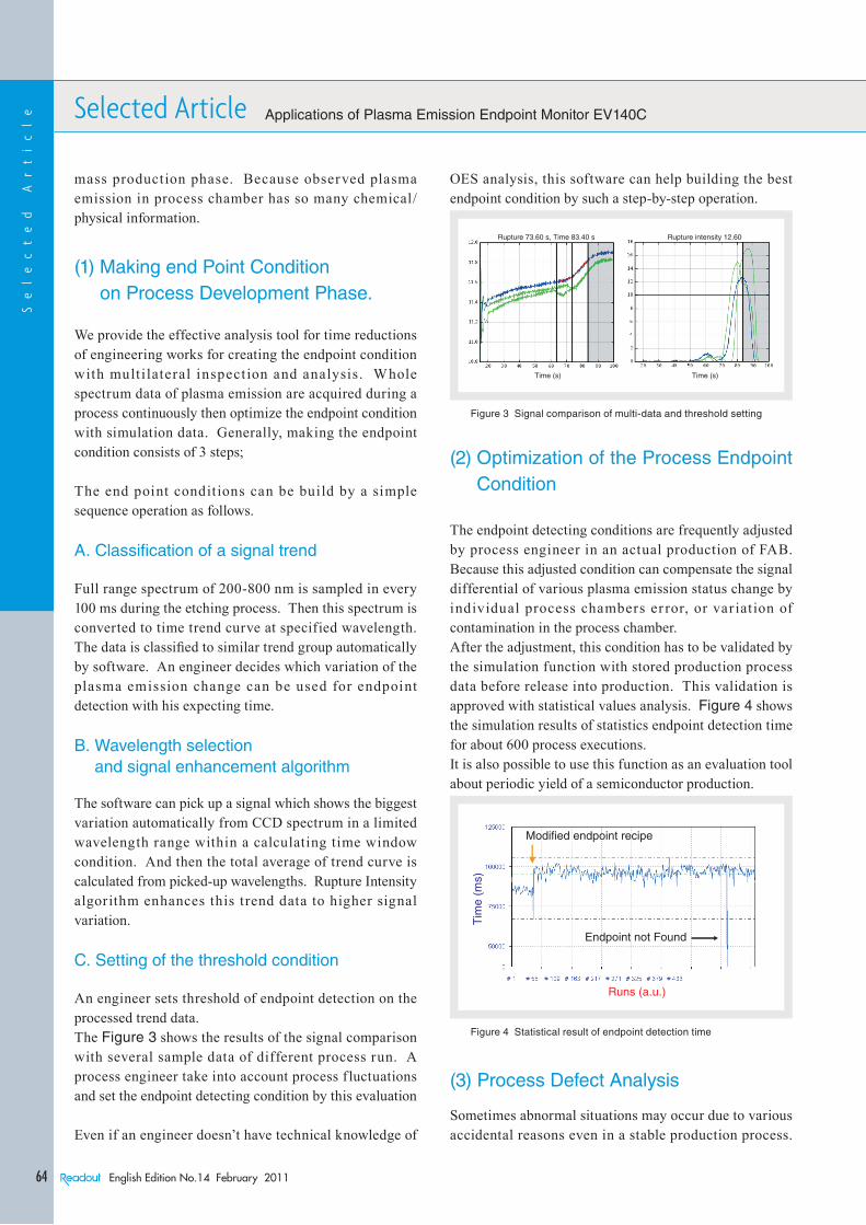
C. Setting of the threshold condition
An engineer sets threshold of endpoint detection on the processed trend data.The Figure 3 shows the results of the signal comparison with several sample data of different process run. A process engineer take into account process f luctuations and set the endpoint detecting condition by this evaluation
Even if an engineer doesn’t have technical knowledge of
OES analysis, this software can help building the best endpoint condition by such a step-by-step operation.
Time (s)
Rupture 73.60 s, Time 83.40 s Rupture intensity 12.60
Time (s)
Figure 3 Signal comparison of multi-data and threshold setting
(2) Optimization of the Process Endpoint Condition
The endpoint detecting conditions are frequently adjusted by process engineer in an actual production of FAB. Because this adjusted condition can compensate the signal differential of various plasma emission status change by individual process chambers er ror, or var iation of contamination in the process chamber.After the adjustment, this condition has to be validated by the simulation function with stored production process data before release into production. This validation is approved with statistical values analysis. Figure 4 shows the simulation results of statistics endpoint detection time for about 600 process executions.It is also possible to use this function as an evaluation tool about periodic yield of a semiconductor production.
Endpoint not Found
Runs (a.u.)
Tim
e (m
s)
Modified endpoint recipe
Figure 4 Statistical result of endpoint detection time
(3) Process Defect Analysis
Sometimes abnormal situations may occur due to various accidental reasons even in a stable production process.

Selected Article Applications of Plasma Emission Endpoint Monitor EV140C
English Edition No.14 February 2011
Technical Reports
65
We can assume that there are various factors of this reason from the process gas supplying system, RF power, the pressure and a gas leak, etc. Our system is possible to observe such abnormal process from f luctuations of a plasma emission. In the case of Figure 5, N2 gas leak is supposed to occur in the process chamber. And spectrum changes in 650 nm band and 750 nm band are observed in a particular peak by N2 gas. This system can be used for plasma condition management by observing the full spectrum monitoring and build together this process defects detection into standard endpoint condition.
0
10
20
30
40
50
60
70
80
90
100
Sig
nal i
nten
sity
(a.
u.)
Wavelength (nm)
450 550 650 750250 350
N2 Leak Standard condition
N2 atomic Lines
Figure 5 plasma condition monitor from N2 gas leak
Summary
The high-performance spectroscopic system, real-time measurements, high-speed calculations and sensitive endpoint detection algorithms, these key issues are requ i red in semiconductor manufact u r ing. The engineering software supports task load reducing of c o m plex e ng i n e e r i ng wo r k fo r p r o c e s s r e c ip e optimization. We believe that EV-140C is a total solution tool for the manufacturing management requests from semiconductor industry.
References
[1] HORIBA Jobin Yvon, OES Engineering & Dry Etch Process Control, 2008
Hiroshi IidaSemiconductor Instrument Development Dept.Application CenterHORIBA Ltd.