reactive power control of single phase grid tied voltage ... · reactive power control of single...
TRANSCRIPT
Reactive Power Control of Single Phase Grid Tied Voltage Sourced Inverters for Residential PV
Application
Xiangdong Zong Department of Electrical and
Computer Engineering
University of Toronto
Toronto, Ontario, Canada M5S 3G4
Email: [email protected]
Abstract-This paper introduces a reactive power control method for a grid tied single phase Voltage Sourced I nverter (VSI), which is used for residential photovoltaic (PV) power integration. The focus is on designing a low complexity grid synchronization method, which decouples the active and reactive power component so that each component can be controlled independently. The AC current and DC voltage controllers for the VSI are briefly discussed. The design and analysis of the grid synchronization method are described in detail. Experimental results validate the effectiveness of the controller and the reactive power control ability.
I. INTRODUCTION
As more distributed resources (DR), such as solar and wind,
become integrated into the utility grid at the distribution level,
the trend that the DR units actively supply reactive power
to the grid has appeared. Having the capability of supplying
reactive power, these DRs will help in supporting local grid
voltage and reducing the burden of delivering reactive power
from central generation to the local distribution level for
compensating of inductive load [1 ]-[4].
Although purposeful injection of reactive power or attempt
ing to support grid voltage by a distributed generator is not
currently permitted by the IEEE 1547-2003 grid integration
standard [5], next generation grid codes for DRs are an
ticipated to incorporate requirements for ancillary services,
including reactive power compensation to support local grid
voltage [6]. As a result, the ability of single phase grid
interfaced inverters to provide reactive power control will
facilitate compliance with future grid requirements.
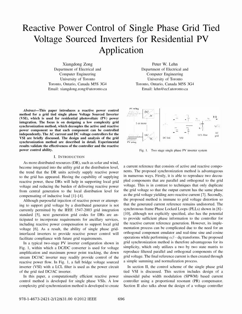
In a typical two-stage PV inverter configuration shown in
Fig. 1, within which a DCIDC converter is used for voltage
amplification and maximum power point tracking, the down
stream DCI AC inverter may readily provide control of the
reactive power flow. In Fig. 1, a full bridge voltage sourced
inverter (VSI) with a LCL filter is used as the power circuit
of the grid tied DCI AC inverter.
In this paper, a computationally efficient reactive power
control method is developed for single phase VSIs. A low
complexity grid synchronization method is developed to create
Peter W. Lehn Department of Electrical and
Computer Engineering
University of Toronto
Toronto, Ontario, Canada M5S 3G4
Email: [email protected]
, , : ' lor more
DC link VSI LCLfilter
Fig. 1. Two stage single phase PV inverter system
AC grid
a current reference that consists of active and reactive compo
nents. The proposed synchronization method is advantageous
in numerous ways. Firstly, it is able to reproduce two decou
pled components that are parallel and orthogonal to the grid
voltage. This is in contrast to techniques that only duplicate
the grid voltage so that the output current has the same phase
as the grid voltage yielding zero reactive current [7]. Secondly,
the proposed method is immune to grid voltage distortion so
that the generated current reference remains undistorted. The
synchronous frame Phase Locked Loops (PLLs) shown in [8]
riO], although not explicitly specified, also has the potential
to provide sufficient phase information to the controller for
the reactive current reference generation. However, its imple
mentation process can be complicated due to the need for an
orthogonal component emulator and real-time sine and cosine
operations while performing af3 - dq transforms. The proposed
grid synchronization method is therefore advantageous for its
simplicity, which only utilizes a two by two state matrix to
reproduce filtered parallel and orthogonal components of the
grid voltage. The final reference current is then created through
a simple summing and normalization process.
In section II, the control scheme of the single phase grid
tied VSI is discussed. This section includes design of a
sinusoidal pulse width modulation (SPWM) based current
controller using a proportional resonant (PR) compensator.
Section II also talks about the design of a voltage controller
978-1-4673-2421-2/12/$31.00 ©2012 IEEE 696
+�.
I Hnolch( S) I - �
Vd/ejt()-
-jl� VSI
r I SPWM
��"� �H� + C Vt iT rv Vg-
_ Kl I--- I--
LCL Filter
-g-1
- • ref
Gls) + 19 - �-
DC Voltage Current Control F eed-forward
• ref 19l1 Grid
Gv(s) r � c- Synchronizer t--
• ref t V 19� 9
DC Voltage Control Grid Synchronization
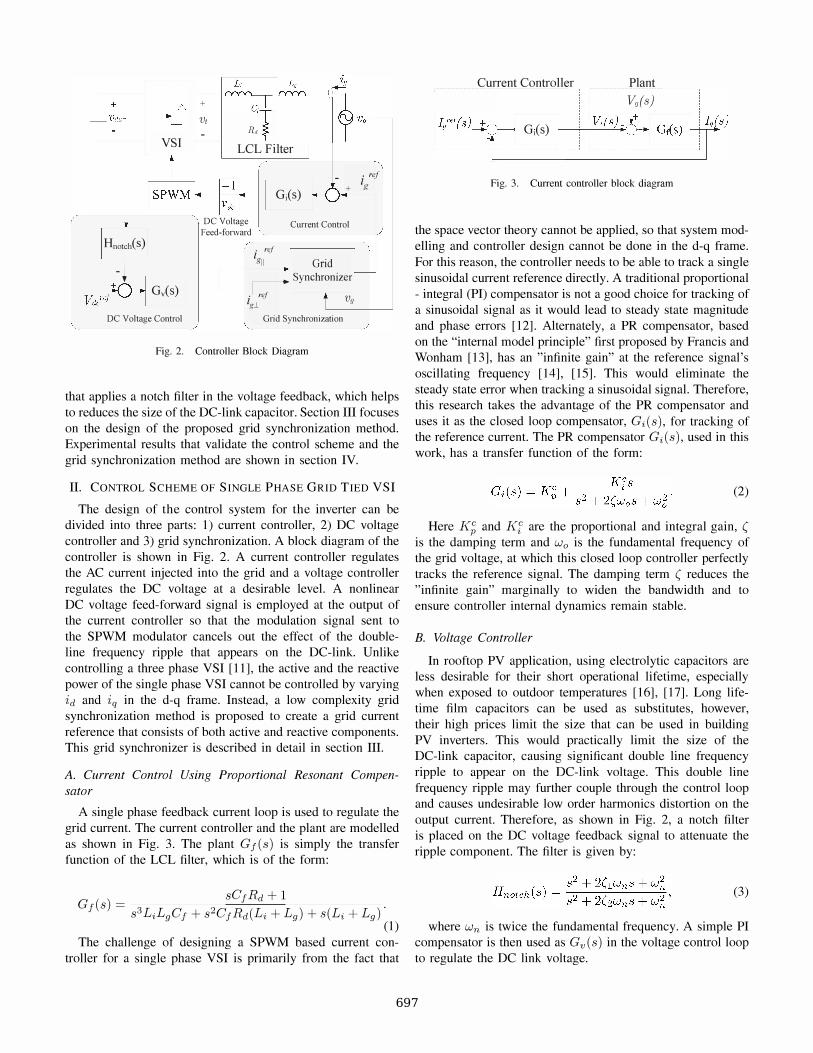
Fig. 2. Controller Block Diagram
that applies a notch filter in the voltage feedback, which helps
to reduces the size of the DC-link capacitor. Section III focuses
on the design of the proposed grid synchronization method.
Experimental results that validate the control scheme and the
grid synchronization method are shown in section IV.
II. CONTROL SCHEME OF SINGLE PHASE GRID TIED VSI
The design of the control system for the inverter can be
divided into three parts: 1) current controller, 2) DC voltage
controller and 3) grid synchronization. A block diagram of the
controller is shown in Fig. 2. A current controller regulates
the AC current injected into the grid and a voltage controller
regulates the DC voltage at a desirable level. A nonlinear
DC voltage feed-forward signal is employed at the output of
the current controller so that the modulation signal sent to
the SPWM modulator cancels out the effect of the double
line frequency ripple that appears on the DC-link. Unlike
controlling a three phase VSI [11], the active and the reactive
power of the single phase VSI cannot be controlled by varying
id and iq in the d-q frame. Instead, a low complexity grid
synchronization method is proposed to create a grid current
reference that consists of both active and reactive components.
This grid synchronizer is described in detail in section III.
A. Current Control Using Proportional Resonant Compen
sator
A single phase feedback current loop is used to regulate the
grid current. The current controller and the plant are modelled
as shown in Fig. 3. The plant G f (s) is simply the transfer
function of the LCL filter, which is of the form:
G ( ) = sC f Rd + 1
f S s3 LiLgCf + s2CfRd(Li + Lg) + S(Li + Lg)' (1)
The challenge of designing a SPWM based current con
troller for a single phase VSI is primarily from the fact that
Current Controller r-------------------------------------------------
iI,rel('!4 I G,(') I c ____________________ == __________________ _
Plant ---------------------------
Vg(s) V,(,!� i��JJr
Fig. 3. Current controller block diagram
the space vector theory cannot be applied, so that system mod
elling and controller design cannot be done in the d-q frame .
For this reason, the controller needs to be able to track a single
sinusoidal current reference directly. A traditional proportional
- integral (PI) compensator is not a good choice for tracking of
a sinusoidal signal as it would lead to steady state magnitude
and phase errors [12]. Alternately, a PR compensator, based
on the "internal model principle" first proposed by Francis and
Wonham [13], has an "infinite gain" at the reference signal's
oscillating frequency [14], [15]. This would eliminate the
steady state error when tracking a sinusoidal signal. Therefore,
this research takes the advantage of the PR compensator and
uses it as the closed loop compensator, Gi(s), for tracking of
the reference current. The PR compensator Gi (s), used in this
work, has a transfer function of the form:
(2)
Here K� and K'f are the proportional and integral gain, (
is the damping term and Wo is the fundamental frequency of
the grid voltage, at which this closed loop controller perfectly
tracks the reference signal. The damping term ( reduces the
"infinite gain" marginally to widen the bandwidth and to
ensure controller internal dynamics remain stable.
B. Voltage Controller
In rooftop PV application, using electrolytic capacitors are
less desirable for their short operational lifetime, especially
when exposed to outdoor temperatures [16], [17]. Long life
time film capacitors can be used as substitutes, however,
their high prices limit the size that can be used in building
PV inverters. This would practically limit the size of the
DC-link capacitor, causing significant double line frequency
ripple to appear on the DC-link voltage. This double line
frequency ripple may further couple through the control loop
and causes undesirable low order harmonics distortion on the
output current. Therefore, as shown in Fig. 2, a notch filter
is placed on the DC voltage feedback signal to attenuate the
ripple component. The filter is given by:
(3)
where Wn is twice the fundamental frequency. A simple PI
compensator is then used as G v (s) in the voltage control loop
to regulate the DC link voltage.
697

1-------'"-----.rYl-----�1 . Tef
�-�EE>�
Vg- 1 Amplitude identifier
�--"'-------'--�
Fig. 4. Grid synchronizer block diagram
Xl
x = Ax + Be y , , -----,=--
y=Cx + De
"----------11 xj=[l 0] y �
v
Fig. 5. Feedback loop of the grid voltage estimator
III. GRID SYNCHRONIZ ATION METHOD FOR GENERATING
ACTIVE AND REACTIVE CURRENT REFERENCE
The grid synchronizer consists of two parts: (i) a grid
voltage estimator, and (ii) an amplitude identifier. An overview
of the grid synchronizer is shown in Fig. 4.
A. Grid Voltage Estimator
The grid voltage estimator takes the grid voltage as its input
and outputs one signal that is aligned with the grid voltage
(parallel component), and a second signal that leads the grid
voltage by 900 (orthogonal component). This estimator is
expressed in the state space form as:
A B
[Xl] �[O wo] [Xl] �[ksYnc] v _ X . 0 x
+
0 (g d X2 -Wo 2 c
[ �:� ] [:: ] � [::]
(4)
The estimator in (4) takes Vg -Xl as its input and outputs
Xl as the parallel component of vg. Thus, this essentially
resembles a feedback loop as illustrated in Fig. 5, where the
output Xl tracks vg• The reference signal of this feedback loop is vg, a sinusoidal
signal oscillating at the grid frequency. The state matrix fl., which is an internal oscillator, oscillates at Woo This provides
the estimator with infinite gain at Wo in the frequency domain.
In (4), the ksync term introduces damping to the oscillator
which widens the estimator's bandwidth and reduces the gain
at woo Therefore, setting Wo to be the fundamental frequency of
the grid results in Xl tracking the input Vg at its fundamental
� � tf.
� � � �
-10 -20 /
/ / -30 / / / /
-40 / / /
-50 /
-60 -70 -80
90
45
-45
-90 10° 10'
/ / /
10' 10' Frequency (rad/sec)
v II(jw) (a) bode plot of _.0--. -Vg(JW)
� � � �
� � � � �
Ksync=100 -- Ksync=300 -. - Ksync=500
- - - Ksync=1000
20r-��� ____ ��B_O_de_D�iag�ra_m� ______ � ____ � ------- --
- _ . - _ . - - .:: .-=...-=-0 - --20 -40 -60 -80
-100 180
135
90
45
0 10°
Fig. 6.
, . , \ '-, '-.� ,
102 103 Frequency (radlsec)
" - ."::..-(b) bode plot of
Vq_djw) Vg(Jw)
Bode plot of voll (;w) and vq.!. (jw) Vg(Jw) Vg(Jw)
frequency, while also rejecting other harmonics that appear on
the grid voltage. On the other hand, X2, based on the solution
of (4), always has the same amplitude as Xl but leads Xl by
900• Consequently, the output YI is denoted as vgll to illustrate
its alignment with the grid voltage and the output Y2 is denoted
as VgJ. to illustrate it is orthogonal to the grid voltage.
The state space form of the compensator ((4» can be further
rewritten to the standard state space form shown in (5), so that
Vg is expressed as the input to the estimator and the outputs
are the parallel component and the orthogonal component of
vg.
A B
[�l] = '[-ksy:c wo]' [Xl] + �[ksync] v X2 -Wo 0 X2 0 (g) (5)
698

c
[ �:� 1 [:: 1 � [::1 The bode plot of each output of the comEensator's responses
are shown in Fig. 6. In Fig. 6a, the ��'d:;; response has a
magnitude of OdB and a phase of 00 at the grid fundamental
frequency and attenuates distortion at any other frequencies.
In Fig. 6b, the ���«jw» response also keeps the magnitude Vg JW at OdB at the grid fundamental frequency but only attenuates
distortion at higher frequencies. Meanwhile, the phase of the ���«(jw» response is at 900 at the grid fundamental frequency Vg JW so that VgJ.. leads Vg by 900• It can also be observed from
Fig. 6 that the more ksync increases, the less the synchro
nizer is sensitive to slight variations of the grid fundamental
frequency, but more vulnerable to noise at other frequencies.
Furthermore, the larger ksync gets, the wider the controller's
bandwidth extends, which means the faster vgll locks on to vg. The start-up trajectories of the state variables Xl and X2
are shown in Fig. 7 for different values of ksync. Zero initial
conditions are assumed in each case. From the two plots,
several observations can be extracted. First, the final state
trajectories are identical circles proving that Xl and X2 are
sinusoidal functions with 900 phase difference. Second, the
radius of the circle is equal to the magnitude of the grid
voltage, indicating that both sinusoidal functions have an
amplitude equal to the magnitude of the grid voltage. This
effectively demonstrates that the grid estimator resembles the
fundamental component of the grid voltage and emulates an
orthogonal component with the same magnitude. Third, with
the initial conditions of states Xl and X2 equal to zero, the
plot with the larger ksync has a faster speed to reach the final
trajectory.
In addition, when setting the grid voltage estimator's in
ternal oscillator's frequency Wo to be 377rads/s (60Hz), the
power factor of the inverter when exposing to different grid
frequencies is computed. Results are shown in Fig. 8 for dif
ferent ksync values. Switching harmonics have been neglected
and the reactive power compensation feature of the inverter
is turned off. One can observe that as ksync gets larger, the
power factors have become more consistent over a broad range
of frequencies.
B. Amplitude Identifier
A grid voltage amplitude identifier is needed to determine
the amplitude of the grid voltage. The amplitude identifier has
the form:
(6)
Equivalently, we may also write l1g v' xi + x� as
graphically displayed in the transient state plane plot of Fig. 7.
Other options of implementing the amplitude identifier may
include peak detection for the grid voltage or peak detection
for either output of the grid voltage estimator. Both methods
X2 X2
Xl
(a) ksync=200 (b) ksync=600 Fig. 7. Start up trajectory of the estimator's state variables for different ksync values
1.05 ,-----,---,----,---,---,----,,-----,---,----,-------,
u:-a. � 0.95 � U. � � I
0.9
0.85 I
I 50 52
_.-.- . -. _ ' =�,-----=�-""". -=. _. -. -'-
/ /
/ I I I
I I
54 56 58 60 62 Freqeuncy (Hz)
, , , , ,
, \
- - - Ksync =200 ....... Ksync=300 - �ync=500
. _. _. '\ync=1000
64 66
, \
\ \
\
68 70
Fig. 8. Power factors vs. grid frequencies for Q=O while neglecting switching harmonics
avoid using the square root operand. However, peak detection
of either vgll or VgJ.. is preferred because the grid voltage
estimator attenuates the harmonic distortion that appears on
the grid voltage, so that the peak detection for the output of
the estimator is more accurate than for the grid voltage itself.
C. Synchronized Current Reference Creation
Once vgll and VgJ.. are obtained from the grid voltage
estimator, and l1g is obtained from the amplitude identifier,
controlling the phase of the current reference becomes possi
ble. Given the grid reference current's parallel and orthogonal
components, i�r and i�1., a synchronized current reference
signal can be obtained as follows:
.ref .ref tgll vgll + tgJ.. VgJ.. ire f = -='--_-;:---"-__ 9 l1g
(7)
Since the parallel component of the current reference i��f is aligned with the grid voltage, this i��f controls the active
power flow to the grid. On the other hand, since the orthogonal
component of the current reference i�1. leads the grid voltage
699

TABLE I INVERTER PARAMETERS AND COMPONEN T VALUES
Grid voltage Vg Rated output current I�ated
DC-link nominal voltage VJ� DC-link Capacitor, Cdc Bridge side inductor Li Grid side inductor Lg
Filter capacitor C f Filter damping resistor Rd Switching frequency Jsw
TABLE II
60V (RMS) lOA (RMS)
140V (RMS) 230/-LF 300/-LH 100/-LH 30/-LF 1.50
30kHz
INVERTER STEADY STATE OPERATION RESULTS
Corresponding Fig Power factor %DC-link ripple (%)
Fig. 9a 17.S Fig. 9b IS.0 Fig. 9c IS. 1
by 900, this i�1. controls the reactive power flow to the grid.
In the overall control system of the single phase VSI, shown
in Fig. 2, i��f is the output of the voltage controller. This
therefore depends on the amount of power that is transferred
by the front end DC/DC converter. i�1. is the user defined
independent input command to synchronizer allowing decou
pled control of reactive power. The value of i�1. is limited by
the current rating of the inverter.
IV EXPERIMENT RESULTS
To verify the effectiveness of the control scheme, an ex
perimental prototype was built. The control system is imple
mented on a 32-bits fixed point microcontroller. Voltage and
current signals are sampled using the internal lO-bit analog
to-digital converter inside the microcontroller. The front end
DC/DC converter is emulated using a constant current source.
The system parameters and component values used for the
experimental setup are listed in Table I.
A. Steady State Response
Fig. 9 shows the steady state operating DC-link voltage
Vdc(t), grid voltage vg(t), and the current flowing into the
grid -ig (t). The inverter is running its rated output current
-ig= lOA (RMS) and a grid frequency of 60Hz. Figs. 9a
through 9c illustrate operating scenarios where the inverter is
generating pure active power, pure reactive power, and a mix
of active and reactive power, respectively. The correspondent
measured results are listed in Table II. These experimental
results demonstrate the reactive power control capability of
the inverter. In addition, it can be seen that with a fairly large
double line frequency voltage ripple presented on the DC-link,
the total demand distortions (TDD) of the output gird current
of all three cases are below 5%. This proves the effectiveness
of the non-linear DC voltage feed-forward signal and the notch
filter in the DC voltage control loop.
B. Transient Response
Fig. lOa shows the transient response of the inverter when
the DC-link voltage steps up from l20V to l40V while the
:��:- AgiltIHtTecllnologies FRIAUG 0516:01 00 2011
-ig(t)
(a) Grid current is in phase with the voltage
:::�:- AgilentTechnologies FRIAUG 0516:18:32 2011
-ig(t)
(b) Grid current lags the voltage by 900
::-�:::- AgilentTechnologies FRIAUG0515:29:192011
-iy{t)
(c) Grid current lags the voltage by 36.80 (PF=O.S, lagging)
Fig. 9. Steady state operation of the inverter
output grid current is kept at OA. The DC voltage transient
response demonstrates good system dynamics where the DC
link voltage settling time is around 20ms and the percentage
overshoot is less than 30%. Fig. lOb shows the step response
of the inverter when the reactive power controlling command
i�1. steps up from OA to lOA (RMS) while DC-link voltage
is kept at constant l40V The i�1. step change demonstrates
good decoupling of the parallel and orthogonal axis of the
controller as the step change in i�1. causes little impact on
the DC-link voltage.
V CONCLUSION
In this paper, a reactive power control method is developed
for single phase VSIs. A PR compensator is used in the current
control loop for tracking a sinusoidal reference current. A
notch filter is added to the DC-link voltage feedback signal to
filter out the double line frequency ripple component appeared
on the DC-link voltage so that the output grid current is not
distorted by this ripple component.
700

A low complexity grid synchronization method is developed
to create a current reference that consists of active and reactive
components. The reactive component i�1 can be used as
the reactive power control conunand which tells the inverter
how much reactive current needs to be injected/absorbed.
This therefore gives the inverter the ability of independently
controlling the reactive power flow. Furthermore, the proposed
grid synchronizer only uses a two by two state matrix to gen
erate the parallel and orthogonal components. This lowers the
implementation complexity and the computational burden on
the digital processor comparing to methods using synchronous
frame PLLs, which require sine and cosine calculations for d
q frame transformation. The drawback of the synchronization
method is that since the grid estimator has a fixed oscillator
frequency wo, exposure to large frequency variation would
result in undesirable power factor degradation (refer to Fig. 8).
Although increasing ksync minimizes the effect, the noise
suppression ability of the estimator would be compromised.
Another drawback of the grid synchronization method is the
need for a square root calculation in the amplitude identi
fier, which could increase the processing time of the digital
processor. A viable solution to this problem is using peak
detection on the output of the estimator to avoid the square
root calculation.
The experimental results prove the effectiveness of the
controller by demonstrating the inverter's ability of generating
pure active power, pure reactive power, and a mix of active
and reactive power. The transient response demonstrates good
dynamic response of the control system.
REFERENCES
[1] K. Turitsyn, P. Sulc, S. Backhaus, and M. Chertkov, "Local control of reactive power by distributed photovoltaic generators," in Smart Grid Communications (SmartGridComm), 2010 First IEEE International Conference on, Oct. 2010, pp. 79 - 84.
[2] E. Paal and Z. Tatai, "Grid connected inverters influence on power quality of smart grid," in Power Electronics and Motion Control Conference
(EPEIPEMC), 2010 14th International, Sept. 2010, pp. T6-35 - T6-39. [3] M. Ettehadi, H. Ghasemi, and S. Vaez-Zadeh, "Reactive power ranking
for dg units in distribution networks," in Environment and Electrical Engineering (EEEIC), 2011 10th International Conference on, May. 2011, pp. 1 - 4.
[4] M. Kandil, M. EI-Saadawi, A. Hassan, and K. Abo-AI-Ez, "A proposed reactive power controUer for dg grid connected systems," in Energy
Conference and Exhibition (EnergyCon), 2010 IEEE International, Dec. 2010, pp. 446 - 451.
[5] "IEEE standard for interconnecting distributed resources with electric power systems," IEEE Std 1547-2003, pp. 1 - 16, 2003.
[6] GJ. Kish and P.W Lehn, "Microgrid design considerations for next generation grid codes (to be published)," in IEEE Power Engineering Society General Meeting, 2012., Jul. 2012.
[7] K. de Souza, M. de Castro, and F. Antunes, "A dc/ac converter for singlephase grid-connected photovoltaic systems," in IECON 02 [Industrial Electronics Society, IEEE 2002 28th Annual Conference of the], vol. 4, Nov. 2002, pp. 3268 - 3273.
[8] H. Cha, T.-K. Vu, and l.-E. Kim, "Design and control of proportionalresonant controller based photovoltaic power conditioning system," in Energy Conversion Congress and Exposition, 2009. ECCE 2009. IEEE, Sept. 2009, pp. 2198 -2205.
[9] M. Ciobotaru, R. Teodorescu, and F. Blaabjerg, "A new single-phase pll structure based on second order generalized integrator," in Power Electronics Specialists Conference, 2006. PESC '06. 37th IEEE, June. 2006, pp. I - 6.
.:��:: . AgilentTechnologies THU AUG 04 17:30:26 2011 10 00 00 D
(a) DC-link voltage step response
.. �.::;. AgilentTechnoiogie5 INEDAl.Kl171S'39492011 llJ]IIJf StOP 1 �El t aaA
�/+ (\ (\ 1/\ \/ 1\/ IV �
1\ !\ f\ (1\ !\ r\ ( � \ I vJt. IV \ l/ \ IV \ l/ , \ /1\ ! 3 \ / \ / . If I / !t fJ \. V (b) Reactive power controlling command i�"1 step response
Fig. 10. Transient response of the inverter
[l0] E. lung and S.-K. Sui, "Implementation of grid-connected single-phase inverter based on fpga," in Applied Power Electronics Conference and Exposition, 2009. APEC 2009. Twenty-Fourth Annual IEEE, Feb. 2009, pp. 889 - 893.
[11] M. Kazmierkowski and L. Malesani, "Current control techniques for three-phase voltage-source pwm converters: a survey," Industrial Elec
tronics, IEEE Transactions on, vol. 45, no. 5, pp. 691 - 703, Oct. 1998. [12] A. Kahrobaeian and S. Farhangi, "Stationary frame current control of
single phase grid connected pv inverters," in Power Electronic Drive Systems Technologies Conference (PEDSTC), 2010 1st, Feb. 2010, pp. 435 - 438.
[l3] B. Francis and W Wonham, "The internal model principle for linear multi variable regulators," 1. Appl. Matlls. Optim., vol. 2, no. 2, pp. 170 - 194, 1975.
[l4] D. Zmood and D. Holmes, "Stationary frame current regulation of pwm inverters with zero steady state error," in Power Electronics Specialists Conference, 1999. PESC 99. 30th Annual IEEE, vol. 2, 1999, pp. 1185 - 1190.
[15] X. Yuan, 1. Allmeling, W Merk, and H. Stemmler, "Stationary frame generalized integrators for current control of active power filters with zero steady state error for current harmonics of concern under unbalanced and distorted operation conditions," in Industry Applications Conference, 2000. Conference Record of the 2000 IEEE, vol. 4, Oct. 2000, pp. 2143 - 2150.
[16] S. Kjaer, J. Pedersen, and F. Blaabjerg, "A review of single-phase gridconnected inverters for photovoltaic modules," Industry Applications, IEEE Transactions on, vol. 41, no. 5, pp. 1292 - 1306, Sept. - Oct. 2005.
[17] E. Leif, "Aluminium electrolytic capacitors' performance in very high ripple current and temperature applications," in Proceedings CARTS Europe 2007 Symposium, Oct. - Nov. 2007, p. 4 of 4.
701