re46c317/re46c318 data sheet - microchip...
TRANSCRIPT
RE46C317/18Piezoelectric Horn Driver with Boost Converter
Features:
• 3V Operation
• Low Quiescent Current
• 10V Boost Converter
• Low Horn Driver On-Resistance
• Compatible with RE46C117
Applications:
• Smoke Detectors
• CO Detectors
• Personal Security Products
• Electronic Toys
Description:
The RE46C317/18 are CMOS piezoelectric horn driverICs with built-in boost converter. They are intended foruse in 3V battery or battery-backed applications. Thecircuits feature a boost converter and a driver circuitsuitable for driving a piezoelectric horn.
The RE46C317/18 are compatible with the RE46C117device and offer lower standby current.
The RE46C317 has three valid states of Horn Enable(tri-state, low and high), while the RE46C318 has onlytwo valid states, low and high.
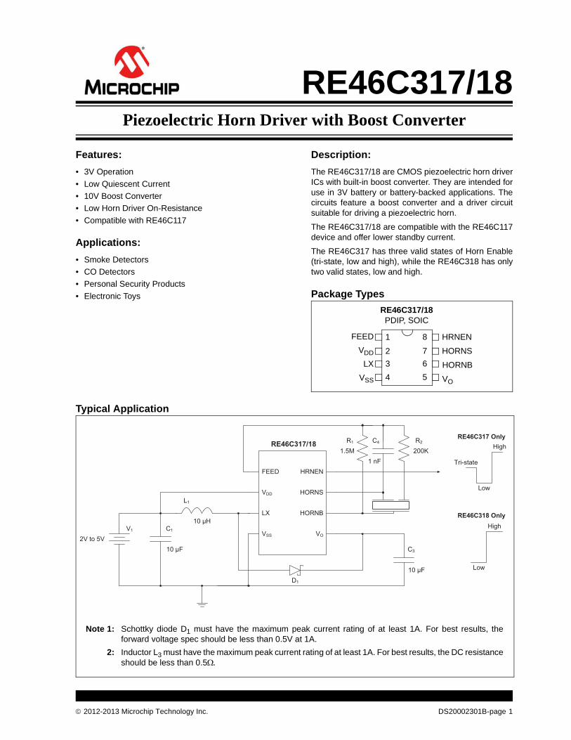
Package Types
Typical Application
1
2
3
4
8
7
6
5
VDD
LX
VSS
FEED HRNEN
HORNS
HORNB
VO
RE46C317/18PDIP, SOIC
EF ED
VDD
HRNEN
HORNS
LX
VSS
HORNB
VO
RE46C317/18
2V to 5V10 μF
10 μH
10 μF
1 nF200K1.5M
RE46C318 Only
Low
High
RE46C317 Only
Low
High
Tri-state
L1
C1
D1
C3
C4 R2R1
V1
Note 1: Schottky diode D1 must have the maximum peak current rating of at least 1A. For best results, theforward voltage spec should be less than 0.5V at 1A.
2: Inductor L3 must have the maximum peak current rating of at least 1A. For best results, the DC resistanceshould be less than 0.5.
2012-2013 Microchip Technology Inc. DS20002301B-page 1

RE46C317/18
Functional Block Diagram
Gate Control
Tri-state LogicLevel Shifter
(RE46C317 Only)
Horn Driver
HRNEN
VSS
LX
HORNS
HORNB
VO
FEED
Standard LogicLevel Shifter
(RE46C318 Only)
Voltage Reference
+
-
+
-
VDD
R1
R2R3
DS20002301B-page 2 2012-2013 Microchip Technology Inc.
RE46C317/18
1.0 ELECTRICAL CHARACTERISTICS
1.1 Absolute Maximum Ratings†
VDD.............................................................................................................................................................................5.5V
VOUT.........................................................................................................................................................................12.5V
Input Voltage Range Except FEED, LX................................................................................VIN = VSS – .3V to VDD + .3V
FEED Input Voltage Range ...........................................................................................................VINFD = -10V to + 22V
LX Input Voltage ...............................................................................................................................VINLX = VOUT + 0.8V
Input Current except FEED, LX ...................................................................................................................... IIN = 10 mA
LX Current (Peak) ...........................................................................................................................................IINLX = 1.0A
Operating Temperature .....................................................................................................................TA = -10C to +60C
Storage Temperature ..................................................................................................................TSTG = -55C to +125C
Continuous Operating Current (HORNS, HORNB, VO) .................................................................................. IO = 40 mA
Maximum Human Body Model ESD........................................................................................................................1500V
† Notice: Stresses above those listed under “Maximum ratings” may cause permanent damage to the device. This is a stress rating only and functional operation of the device at these or any other conditions above those indicated in the operation listings of this specification is not implied. Exposure to maximum rating conditions for extended periods may affect device reliability. This product utilizes CMOS technology with static protection; however proper ESD prevention procedures should be used when handling this product. Damage can occur when exposed to extremely high static electrical charge.
DC ELECTRICAL CHARACTERISTICS – RE46C317Unless otherwise indicated, all parameters apply at TA = -10°C to +60°C, VDD = 3V, VSS = 0V, C3 = 10 µF. Typical values are at TA = +25°C
Parameter SymbolTestPin
Min. Typ. Max. Units Conditions
Supply Voltage VDD 2 2 — 5 V Operating
Standby Supply Current IDD1 2 — 0.5 1 µA HRNEN = Float; No loads
Standby IVO IVO1 5 — 0 0.3 µA HRNEN = Float; No loads
Quiescent Supply Current IDD2 2 — 27 49 µA HRNEN = Low; No Loads; VO = 11V; VL X = 0.5V
Quiescent IVO IVO2 5 — 71 115 µA HRNEN = Low; No Loads; VO = 11V; VL X = 0.5V
Supply current ISUP 2 — 300 — µA HRNEN = Low; No Loads, Boost Running
Input Current for Tri-state IIT 8 -5 — 5 µA HRNEN = Float (Note 4)
Input Voltage High VIHH 8 2.6 — — V HRNEN input
VIHF 1 7 — — V FEED input; VO = 10V
Note 1: The boost converter in Boost mode (normal VO = 10V) can draw current pulses of ~0.8A and therefore is very sensitive to series resistance. The critical components of this resistance are the inductor DC resistance, the internal resistance of the battery and the resistance in the connections from the inductor to the battery, from the inductor to the LX pin. In order to function properly under full load at VDD = 2V, the total of the inductor and the interconnect resistances should not exceed 0.3. The internal battery resistance should be no more than 0.5. A low ESR capacitance of 10 µF or more should be connected in parallel with the battery to average current over the boost converter cycle.
2: In the above table, wherever a specific VO value is listed under test conditions, the VO is forced externally with the inductor disconnected, and the boost converter is not running.
3: The limits shown are 100% tested at +25°C only. Test limits are guard-banded, based on temperature characterization to ensure compliance at temperature extremes.
4: This is the maximum input current that will not cause a logic high or logic low to be asserted.
2012-2013 Microchip Technology Inc. DS20002301B-page 3

RE46C317/18
Input Voltage Low VILH 8 — — 0.4 V HRNEN input
VILF 1 — — 3 V FEED input; VO = 10V
Input Leakage IIHF 1 — 20 50 µA FEED = 22V; VO = 10V
IILF 1 -50 -15 — µA FEED = -10V; VO = 10V
IIHH 8 — 20 50 µA HRNEN = VDD
IILH 8 -50 -20 — µA HRNEN = VSS
Output Leakage IOZH 3 — — 1 µA HRNEN = Float; VO = 12.5V; VLX = 10V
VO Output Voltage VVO 5 9 10 11 V VDD = 3V, HRNEN = Low or High, IOUT = 10 mA
VO Efficiency VOEFF 5 — 80 — % ILOAD = 10 mA, VDD = 3V, HRNEN = 0V
Output Low Voltage VOL 6, 7 — 0.3 0.5 V HORNB or HORNS IOUT = -16 mA, VDD = 3V
Output High Voltage VOH 6, 7 9.5 9.7 — V HORNB or HORNS VO =10V VDD = HRNEN = 3V IOUT = 16 mA
DC ELECTRICAL CHARACTERISTICS – RE46C317 (CONTINUED)Unless otherwise indicated, all parameters apply at TA = -10°C to +60°C, VDD = 3V, VSS = 0V, C3 = 10 µF. Typical values are at TA = +25°C
Parameter SymbolTestPin
Min. Typ. Max. Units Conditions
Note 1: The boost converter in Boost mode (normal VO = 10V) can draw current pulses of ~0.8A and therefore is very sensitive to series resistance. The critical components of this resistance are the inductor DC resistance, the internal resistance of the battery and the resistance in the connections from the inductor to the battery, from the inductor to the LX pin. In order to function properly under full load at VDD = 2V, the total of the inductor and the interconnect resistances should not exceed 0.3. The internal battery resistance should be no more than 0.5. A low ESR capacitance of 10 µF or more should be connected in parallel with the battery to average current over the boost converter cycle.
2: In the above table, wherever a specific VO value is listed under test conditions, the VO is forced externally with the inductor disconnected, and the boost converter is not running.
3: The limits shown are 100% tested at +25°C only. Test limits are guard-banded, based on temperature characterization to ensure compliance at temperature extremes.
4: This is the maximum input current that will not cause a logic high or logic low to be asserted.
DS20002301B-page 4 2012-2013 Microchip Technology Inc.
RE46C317/18
DC ELECTRICAL CHARACTERISTICS - RE46C318Unless otherwise indicated, all parameters apply at TA = -10°C to +60°C, VDD = 3V, VSS = 0V, C3 = 10 µF. Typical values are at TA = +25°C.
Parameter SymbolTestPin
Min. Typ. Max. Units Conditions
Supply Voltage VDD 2 2 — 5 V Operating
Standby Supply Current IDD1 2 — — 0.1 µA HRNEN = Low; No loads
Input Voltage High VIHH 8 2.3 — — V HRNEN input
VIHF 1 7 — — V FEED input; VO = 10V
Input Voltage Low VILH 8 — — 1 V HRNEN input
VILF 1 — — 3 V FEED input; VO = 10V
Input Leakage IIHF 1 — 20 50 µA FEED = 22V; VO = 10V
IILF 1 -50 -15 — µA FEED = -10V; VO = 10V
IIN 8 -100 — 100 nA HRNEN = VDD or VSS
Output Leakage IOZH 3 — — 1 µA HRNEN = VSS, VO = 12.5V, VLX = 10V
VO Output Voltage VVO 5 9 10 11 V VDD = 3V, HRNEN = High, IOUT = 10 mA
VO Efficiency VVOEFF 5 — 80 — % ILOAD = 10 mA, VDD = 3V, HRNEN = 0V
Output Low Voltage VOL 6, 7 — 0.3 0.5 V HORNB or HORNS; IOUT = -16 mA; VDD = 3V
Output High Voltage VOH 6, 7 9.5 9.7 — V HORNB or HORNS; VO = 10V; VDD = HRNEN = 3V; IOUT = 16 mA
AC ELECTRICAL CHARACTERISTICSUnless otherwise indicated, all parameters apply at TA = -10°C to +60°C, VDD = 3V, VSS = 0V, C3 = 10 µF. Typical values are at TA = +25°C.
Parameter Symbol Test Pin Min. Typ. Max. Units Conditions
Horn Delay THRN 8/6 or 8/7 — — 1 ms HRNEN = High; Boost Running; 16 mA Load
Note 1: Horn Delay is the delay between a high signal on HRNEN and the horn output turning ON. The internal circuitry delays the horn output until the Boost voltage reaches its set point, 10V nominally.
TEMPERATURE CHARACTERISTICSElectrical Characteristics: Unless otherwise indicated, VDD = 3V, VSS = 0V
Parameter Symbol Min. Typ. Max. Units Conditions
Temperature Ranges
Operating Temperature Range TA -10 — 60 °C
Storage Temperature Range TSTG -55 — 125 °C
Thermal Package Resistances
Thermal Resistance, 8L-PDIP JA — 89.3 — °C/W
Thermal Resistance, 8L-SOIC JA — 149.5 — °C/W
2012-2013 Microchip Technology Inc. DS20002301B-page 5
RE46C317/18
NOTES:
DS20002301B-page 6 2012-2013 Microchip Technology Inc.
RE46C317/18
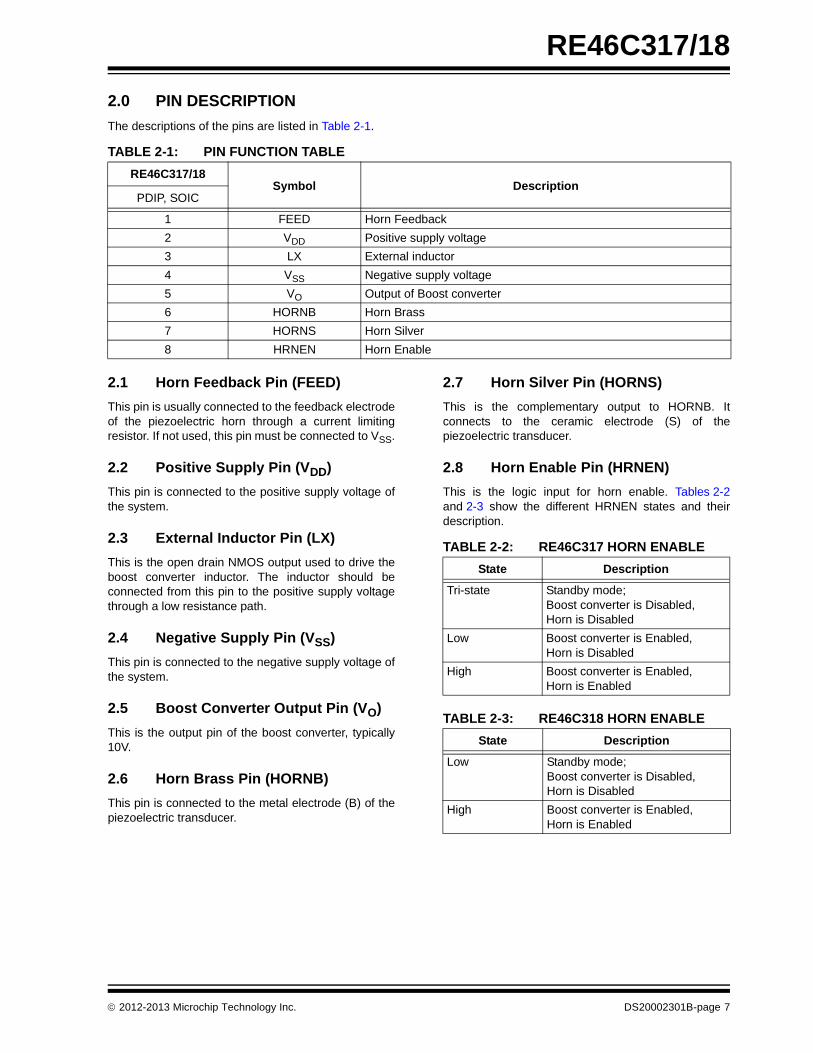
2.0 PIN DESCRIPTION
The descriptions of the pins are listed in Table 2-1.
2.1 Horn Feedback Pin (FEED)
This pin is usually connected to the feedback electrodeof the piezoelectric horn through a current limitingresistor. If not used, this pin must be connected to VSS.
2.2 Positive Supply Pin (VDD)
This pin is connected to the positive supply voltage ofthe system.
2.3 External Inductor Pin (LX)
This is the open drain NMOS output used to drive theboost converter inductor. The inductor should beconnected from this pin to the positive supply voltagethrough a low resistance path.
2.4 Negative Supply Pin (VSS)
This pin is connected to the negative supply voltage ofthe system.
2.5 Boost Converter Output Pin (VO)
This is the output pin of the boost converter, typically10V.
2.6 Horn Brass Pin (HORNB)
This pin is connected to the metal electrode (B) of thepiezoelectric transducer.
2.7 Horn Silver Pin (HORNS)
This is the complementary output to HORNB. Itconnects to the ceramic electrode (S) of thepiezoelectric transducer.
2.8 Horn Enable Pin (HRNEN)
This is the logic input for horn enable. Tables 2-2and 2-3 show the different HRNEN states and theirdescription.
TABLE 2-1: PIN FUNCTION TABLE
RE46C317/18Symbol Description
PDIP, SOIC
1 FEED Horn Feedback
2 VDD Positive supply voltage
3 LX External inductor
4 VSS Negative supply voltage
5 VO Output of Boost converter
6 HORNB Horn Brass
7 HORNS Horn Silver
8 HRNEN Horn Enable
TABLE 2-2: RE46C317 HORN ENABLE
State Description
Tri-state Standby mode; Boost converter is Disabled, Horn is Disabled
Low Boost converter is Enabled, Horn is Disabled
High Boost converter is Enabled, Horn is Enabled
TABLE 2-3: RE46C318 HORN ENABLE
State Description
Low Standby mode; Boost converter is Disabled, Horn is Disabled
High Boost converter is Enabled, Horn is Enabled
2012-2013 Microchip Technology Inc. DS20002301B-page 7

RE46C317/18
NOTES:
DS20002301B-page 8 2012-2013 Microchip Technology Inc.
RE46C317/18
3.0 DEVICE DESCRIPTION
RE46C317 and RE46C318 have three main blocks:
• Horn driver
• Boost regulator
• Horn Enable logic
The following sections describe these blocks.
3.1 Horn Driver
The horn driver is a push-pull circuit, capable of drivinga three-terminal piezoelectric horn. It can also drive amodified two-terminal Piezo horn.
3.2 Horn Enable
In RE46C317, the HRNEN is a tri-state signal withthree valid states: low, high and tri-state (or mid-supply). The three levels of HRNEN determine themodes of operation.
When HRNEN is in tri-state, the device is in Standbymode and all circuits are disabled. This is the lowestcurrent operating mode.
When HRNEN is low, the device is in Boost-Only mode.In this mode, only the boost regulator is enabled andthe output voltage is boosted to 10V nominally. Thehorn driver circuit is disabled in this mode. This modecan be used to check for a low battery condition.
When HRNEN is high, the part is in Normal Operation.The boost regulator and the horn driver circuits areenabled in this mode.
The RE46C318 uses a binary logic circuit, rather thantri-state logic, to determine the mode of operation.
When HRNEN is low, the boost and horn driver circuitsare disabled and the device is in Standby. This is thelowest current operating mode.
When HRNEN is high, the boost and horn drivercircuits are enabled.
3.3 Boost Regulator
The boost regulator in the RE46C317/18 is acurrent-mode controller with two control loops, thatwork together in maintaining a constant output voltageand supply the required load current. The inner currentcontrol loop provides cycle-by-cycle current limiting,while the outer control loop provides output voltagecontrol. When the boost converter is turned on usingthe HRNEN input, the NMOS switch turns on and theinductor current ramps up to its peak value,approximately 0.6A nominally.
The current comparator turns off the NMOS switch fora fixed period of time to allow energy to be transferredto the output capacitor. When the voltage on the outputcapacitor equals or exceeds the desired output voltage,10V nominally, the current loop is disabled until theload discharges the output capacitor to a voltage lowerthan the desired output voltage.
Every time the output voltage falls below the desiredvalue, the switching cycle starts and continues until thedesired value is reached. The constant switchingresulting in the charging and discharging of the outputcapacitor causes a ripple on the output voltage. Theripple on the output voltage depends on the externalcomponent parameters, such as the value of externalcapacitor, its ESR, etc.
In both RE46C317 and RE46C318, when logic high isasserted on the HRNEN pin, the boost regulator isenabled. However, the horn output is not enabled untilthe output voltage reaches its nominal set point, 10Vnominally. This ensures that the output voltage risesquickly to the necessary drive voltage for the Piezohorn.
The boost regulator has been optimized to work withthe external components as shown in the TypicalApplication circuit.
2012-2013 Microchip Technology Inc. DS20002301B-page 9

RE46C317/18
Figure 3-1 shows the horn turn-on delay after theHRNEN has been asserted high. After the boostvoltage reaches its nominal set point, the HORNBoutput turns on. In this case, the HORNB output isdriving a load current of 20 mA DC.
FIGURE 3-1: RE46C317 Horn Turn-On Delay.
Figure 3-2 shows the typical switching waveforms ofthe boost regulator. The top waveform shows the boostoutput, the center waveform shows the LX switchingwaveform, and the lower waveform shows the inductorcurrent.
FIGURE 3-2: RE46C317/18 Switching Waveforms.
DS20002301B-page 10 2012-2013 Microchip Technology Inc.
RE46C317/18
4.0 PACKAGING INFORMATION
4.1 Package Marking Information
8-Lead PDIP (300 mil) Example
XXXXXXXXXXXXXNNN
YYWW
8-Lead SOIC (3.90 mm) Example
NNN
Legend: XX...X Customer-specific informationY Year code (last digit of calendar year)YY Year code (last 2 digits of calendar year)WW Week code (week of January 1 is week ‘01’)NNN Alphanumeric traceability code Pb-free JEDEC designator for Matte Tin (Sn)* This package is Pb-free. The Pb-free JEDEC designator ( )
can be found on the outer packaging for this package.
Note: In the event the full Microchip part number cannot be marked on one line, it willbe carried over to the next line, thus limiting the number of availablecharacters for customer-specific information.
3e
3e
RE46C318V/P ^^256
13153e
RE46C317SN ^^1315
2563e
2012-2013 Microchip Technology Inc. DS20002301B-page 11

RE46C317/18
���������� ���������� ������������� ����������
�������� ������ �!"�����#�$�%��&"��'��� ��(�)"&�'"!&�)�����&�#�*�&��&�����&���#������� +������%����&�,����&��!&���-� ��'��!��!�����#�.��#��&�����"#��'�#�%��!����&"!��!����#�%��!����&"!��!�!������&��$���#�����/����!�#���� ��'��!��������#�&���������������.�0������
1�,2�1�!�����'��!���� ���&��������$��&� ��"��!�*��*�&�"&�&������!�
����� 3�&���'!&��"��&����4����#�*���!(�����!��!���&��������������4�����������%���&������&�#��&��&&�255***�'��������'5���4�����
6��&! �7,8.���'��!���9�'�&! ��7 7:� ��;
7"')��%����! 7 <��&�� � �����1�, ��&����&��������� � = = ������#�#����4���� ���4��!! �� ���� ��-� ����1�!��&����&��������� �� ���� = =��"�#��&���"�#��>�#&� . ���� �-�� �-����#�#����4����>�#&� .� ���� ���� ��<�: �����9���&� � �-�< �-?� ���� ���&����&��������� 9 ���� ��-� ����9��#� ���4��!! � ���< ���� ����6����9��#�>�#&� )� ���� ��?� ����9*��9��#�>�#&� ) ���� ���< ����: ������*����������+ �1 = = ��-�
N
E1
NOTE 1
D
1 2 3
A
A1
A2
L
b1b
e
E
eB
c
������� ������� ��*��� ,�����<1
DS20002301B-page 12 2012-2013 Microchip Technology Inc.
RE46C317/18
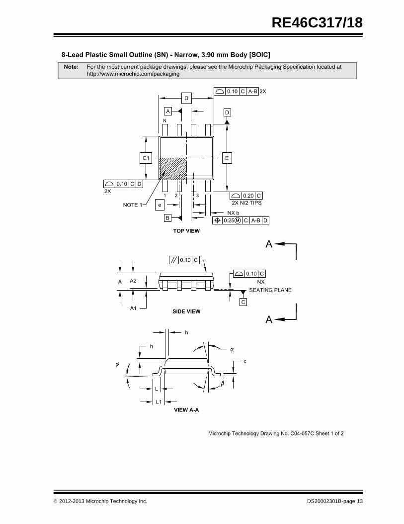
Note: For the most current package drawings, please see the Microchip Packaging Specification located at http://www.microchip.com/packaging
2012-2013 Microchip Technology Inc. DS20002301B-page 13

RE46C317/18
Note: For the most current package drawings, please see the Microchip Packaging Specification located at http://www.microchip.com/packaging
DS20002301B-page 14 2012-2013 Microchip Technology Inc.

RE46C317/18
���������� �� ���!�� ���� �������""�#$��%&����������� !�'�
����� 3�&���'!&��"��&����4����#�*���!(�����!��!���&��������������4�����������%���&������&�#��&��&&�255***�'��������'5���4�����
2012-2013 Microchip Technology Inc. DS20002301B-page 15

RE46C317/18
NOTES:
DS20002301B-page 16 2012-2013 Microchip Technology Inc.
RE46C317/18
APPENDIX A: REVISION HISTORY
Revision B (May 2013)
The following has been modified:
1. Added Maximum Human Body Model ESDvalue to Section 1.1, Absolute MaximumRatings†.
Revision A (June 2012)
• Original Release of this Document.
2012-2013 Microchip Technology Inc. DS20002301B-page 17

RE46C317/18
NOTES:
DS20002301B-page 18 2012-2013 Microchip Technology Inc.
RE46C317/18
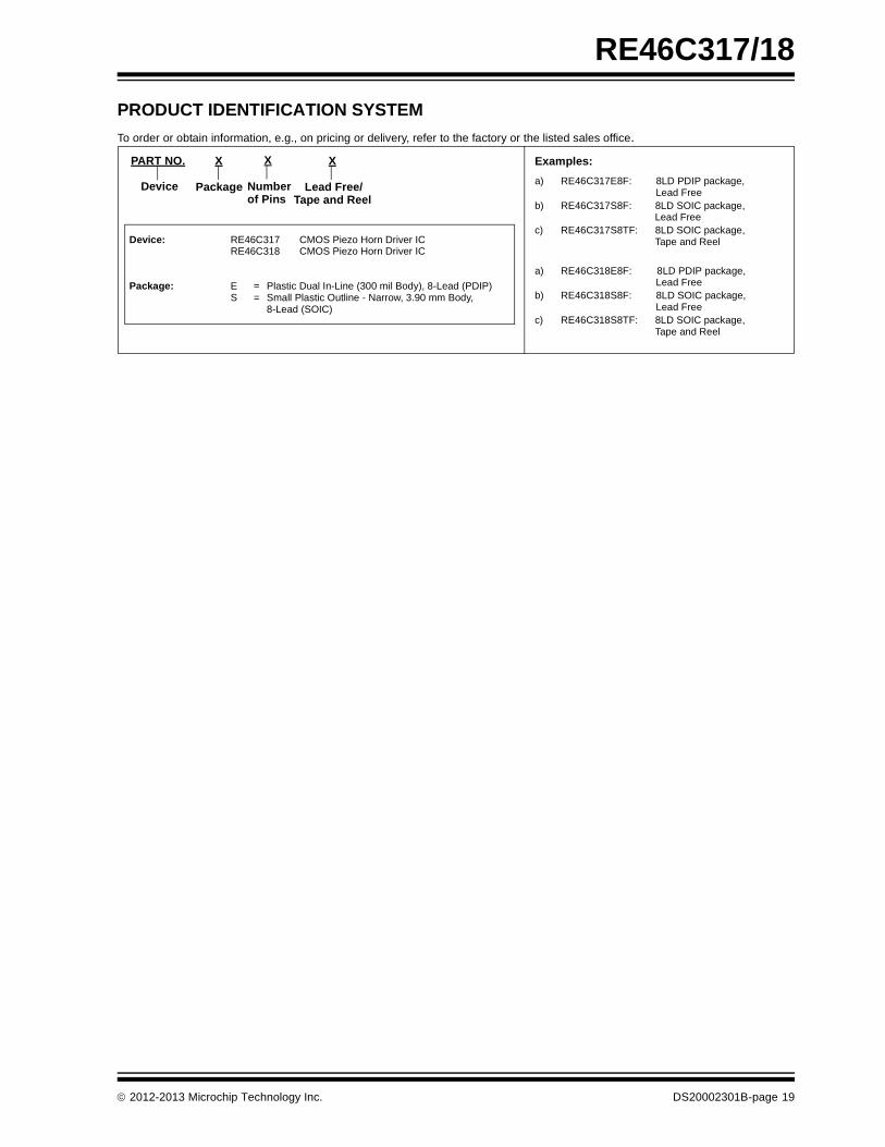
PRODUCT IDENTIFICATION SYSTEM
To order or obtain information, e.g., on pricing or delivery, refer to the factory or the listed sales office.
PART NO. X X
Lead Free/PackageDevice
Device: RE46C317 CMOS Piezo Horn Driver ICRE46C318 CMOS Piezo Horn Driver IC
Package: E = Plastic Dual In-Line (300 mil Body), 8-Lead (PDIP)S = Small Plastic Outline - Narrow, 3.90 mm Body,
8-Lead (SOIC)
Examples:
a) RE46C317E8F: 8LD PDIP package,Lead Free
b) RE46C317S8F: 8LD SOIC package,Lead Free
c) RE46C317S8TF: 8LD SOIC package,Tape and Reel
a) RE46C318E8F: 8LD PDIP package,Lead Free
b) RE46C318S8F: 8LD SOIC package,Lead Free
c) RE46C318S8TF: 8LD SOIC package,Tape and Reel
X
Number of Pins Tape and Reel
2012-2013 Microchip Technology Inc. DS20002301B-page 19

RE46C317/18
NOTES:
DS20002301B-page 20 2012-2013 Microchip Technology Inc.

Note the following details of the code protection feature on Microchip devices:
• Microchip products meet the specification contained in their particular Microchip Data Sheet.
• Microchip believes that its family of products is one of the most secure families of its kind on the market today, when used in the intended manner and under normal conditions.
• There are dishonest and possibly illegal methods used to breach the code protection feature. All of these methods, to our knowledge, require using the Microchip products in a manner outside the operating specifications contained in Microchip’s Data Sheets. Most likely, the person doing so is engaged in theft of intellectual property.
• Microchip is willing to work with the customer who is concerned about the integrity of their code.
• Neither Microchip nor any other semiconductor manufacturer can guarantee the security of their code. Code protection does not mean that we are guaranteeing the product as “unbreakable.”
Code protection is constantly evolving. We at Microchip are committed to continuously improving the code protection features of ourproducts. Attempts to break Microchip’s code protection feature may be a violation of the Digital Millennium Copyright Act. If such actsallow unauthorized access to your software or other copyrighted work, you may have a right to sue for relief under that Act.
Information contained in this publication regarding deviceapplications and the like is provided only for your convenienceand may be superseded by updates. It is your responsibility toensure that your application meets with your specifications.MICROCHIP MAKES NO REPRESENTATIONS ORWARRANTIES OF ANY KIND WHETHER EXPRESS ORIMPLIED, WRITTEN OR ORAL, STATUTORY OROTHERWISE, RELATED TO THE INFORMATION,INCLUDING BUT NOT LIMITED TO ITS CONDITION,QUALITY, PERFORMANCE, MERCHANTABILITY ORFITNESS FOR PURPOSE. Microchip disclaims all liabilityarising from this information and its use. Use of Microchipdevices in life support and/or safety applications is entirely atthe buyer’s risk, and the buyer agrees to defend, indemnify andhold harmless Microchip from any and all damages, claims,suits, or expenses resulting from such use. No licenses areconveyed, implicitly or otherwise, under any Microchipintellectual property rights.
2012-2013 Microchip Technology Inc.
QUALITY MANAGEMENT SYSTEM CERTIFIED BY DNV
== ISO/TS 16949 ==
Trademarks
The Microchip name and logo, the Microchip logo, dsPIC, FlashFlex, KEELOQ, KEELOQ logo, MPLAB, PIC, PICmicro, PICSTART, PIC32 logo, rfPIC, SST, SST Logo, SuperFlash and UNI/O are registered trademarks of Microchip Technology Incorporated in the U.S.A. and other countries.
FilterLab, Hampshire, HI-TECH C, Linear Active Thermistor, MTP, SEEVAL and The Embedded Control Solutions Company are registered trademarks of Microchip Technology Incorporated in the U.S.A.
Silicon Storage Technology is a registered trademark of Microchip Technology Inc. in other countries.
Analog-for-the-Digital Age, Application Maestro, BodyCom, chipKIT, chipKIT logo, CodeGuard, dsPICDEM, dsPICDEM.net, dsPICworks, dsSPEAK, ECAN, ECONOMONITOR, FanSense, HI-TIDE, In-Circuit Serial Programming, ICSP, Mindi, MiWi, MPASM, MPF, MPLAB Certified logo, MPLIB, MPLINK, mTouch, Omniscient Code Generation, PICC, PICC-18, PICDEM, PICDEM.net, PICkit, PICtail, REAL ICE, rfLAB, Select Mode, SQI, Serial Quad I/O, Total Endurance, TSHARC, UniWinDriver, WiperLock, ZENA and Z-Scale are trademarks of Microchip Technology Incorporated in the U.S.A. and other countries.
SQTP is a service mark of Microchip Technology Incorporated in the U.S.A.
GestIC and ULPP are registered trademarks of Microchip Technology Germany II GmbH & Co. KG, a subsidiary of Microchip Technology Inc., in other countries.
All other trademarks mentioned herein are property of their respective companies.
© 2012-2013, Microchip Technology Incorporated, Printed in the U.S.A., All Rights Reserved.
Printed on recycled paper.
ISBN: 978-1-62077-213-3
Microchip received ISO/TS-16949:2009 certification for its worldwide
DS20002301B-page 21
headquarters, design and wafer fabrication facilities in Chandler and Tempe, Arizona; Gresham, Oregon and design centers in California and India. The Company’s quality system processes and procedures are for its PIC® MCUs and dsPIC® DSCs, KEELOQ® code hopping devices, Serial EEPROMs, microperipherals, nonvolatile memory and analog products. In addition, Microchip’s quality system for the design and manufacture of development systems is ISO 9001:2000 certified.
DS20002301B-page 22 2012-2013 Microchip Technology Inc.
AMERICASCorporate Office2355 West Chandler Blvd.Chandler, AZ 85224-6199Tel: 480-792-7200 Fax: 480-792-7277Technical Support: http://www.microchip.com/supportWeb Address: www.microchip.com
AtlantaDuluth, GA Tel: 678-957-9614 Fax: 678-957-1455
BostonWestborough, MA Tel: 774-760-0087 Fax: 774-760-0088
ChicagoItasca, IL Tel: 630-285-0071 Fax: 630-285-0075
ClevelandIndependence, OH Tel: 216-447-0464 Fax: 216-447-0643
DallasAddison, TX Tel: 972-818-7423 Fax: 972-818-2924
DetroitFarmington Hills, MI Tel: 248-538-2250Fax: 248-538-2260
IndianapolisNoblesville, IN Tel: 317-773-8323Fax: 317-773-5453
Los AngelesMission Viejo, CA Tel: 949-462-9523 Fax: 949-462-9608
Santa ClaraSanta Clara, CA Tel: 408-961-6444Fax: 408-961-6445
TorontoMississauga, Ontario, CanadaTel: 905-673-0699 Fax: 905-673-6509
ASIA/PACIFICAsia Pacific OfficeSuites 3707-14, 37th FloorTower 6, The GatewayHarbour City, KowloonHong KongTel: 852-2401-1200Fax: 852-2401-3431
Australia - SydneyTel: 61-2-9868-6733Fax: 61-2-9868-6755
China - BeijingTel: 86-10-8569-7000 Fax: 86-10-8528-2104
China - ChengduTel: 86-28-8665-5511Fax: 86-28-8665-7889
China - ChongqingTel: 86-23-8980-9588Fax: 86-23-8980-9500
China - HangzhouTel: 86-571-2819-3187 Fax: 86-571-2819-3189
China - Hong Kong SARTel: 852-2943-5100 Fax: 852-2401-3431
China - NanjingTel: 86-25-8473-2460Fax: 86-25-8473-2470
China - QingdaoTel: 86-532-8502-7355Fax: 86-532-8502-7205
China - ShanghaiTel: 86-21-5407-5533 Fax: 86-21-5407-5066
China - ShenyangTel: 86-24-2334-2829Fax: 86-24-2334-2393
China - ShenzhenTel: 86-755-8864-2200 Fax: 86-755-8203-1760
China - WuhanTel: 86-27-5980-5300Fax: 86-27-5980-5118
China - XianTel: 86-29-8833-7252Fax: 86-29-8833-7256
China - XiamenTel: 86-592-2388138 Fax: 86-592-2388130
China - ZhuhaiTel: 86-756-3210040 Fax: 86-756-3210049
ASIA/PACIFICIndia - BangaloreTel: 91-80-3090-4444 Fax: 91-80-3090-4123
India - New DelhiTel: 91-11-4160-8631Fax: 91-11-4160-8632
India - PuneTel: 91-20-2566-1512Fax: 91-20-2566-1513
Japan - OsakaTel: 81-6-6152-7160 Fax: 81-6-6152-9310
Japan - TokyoTel: 81-3-6880- 3770 Fax: 81-3-6880-3771
Korea - DaeguTel: 82-53-744-4301Fax: 82-53-744-4302
Korea - SeoulTel: 82-2-554-7200Fax: 82-2-558-5932 or 82-2-558-5934
Malaysia - Kuala LumpurTel: 60-3-6201-9857Fax: 60-3-6201-9859
Malaysia - PenangTel: 60-4-227-8870Fax: 60-4-227-4068
Philippines - ManilaTel: 63-2-634-9065Fax: 63-2-634-9069
SingaporeTel: 65-6334-8870Fax: 65-6334-8850
Taiwan - Hsin ChuTel: 886-3-5778-366Fax: 886-3-5770-955
Taiwan - KaohsiungTel: 886-7-213-7828Fax: 886-7-330-9305
Taiwan - TaipeiTel: 886-2-2508-8600 Fax: 886-2-2508-0102
Thailand - BangkokTel: 66-2-694-1351Fax: 66-2-694-1350
EUROPEAustria - WelsTel: 43-7242-2244-39Fax: 43-7242-2244-393Denmark - CopenhagenTel: 45-4450-2828 Fax: 45-4485-2829
France - ParisTel: 33-1-69-53-63-20 Fax: 33-1-69-30-90-79
Germany - MunichTel: 49-89-627-144-0 Fax: 49-89-627-144-44
Italy - Milan Tel: 39-0331-742611 Fax: 39-0331-466781
Netherlands - DrunenTel: 31-416-690399 Fax: 31-416-690340
Spain - MadridTel: 34-91-708-08-90Fax: 34-91-708-08-91
UK - WokinghamTel: 44-118-921-5869Fax: 44-118-921-5820
Worldwide Sales and Service
11/29/12