radiation hard setp-up dc-dc converteree07229/documents/pdi_ee07229_final...radiation hard setp-up...
TRANSCRIPT

FACULDADE DE ENGENHARIA DA UNIVERSIDADE DO PORTO
Radiation Hard Setp-up DC-DCConverter
Helena Isabel Pais Ferreira de Vargas
Mestrado Integrado em Engenharia Eletrotécnica e de Computadores
Supervisor: Professor José Machado da Silva (PhD)
Second Supervisor: Paulo Moreira
July 6, 2012

c© Helena Vargas, 2012
Abstract
The present document is an introductory work containing research material about radiation hardDC-DC converters. In the future it will be used as background research for a master’s academicdissertation on the subject. First is presented the literature review. After a brief overview onDC-DC converters, the basic operation principles of the step-up converter are described, the semi-conductors currently used in this kind of application are analysed. A brief description of the basiccontrol method and a small introduction of the CMOS technology are made. Then, the state of theart is presented. Some variations of the basic configuration of the step-up converter are shown aswell as the implementation of DC-DC converters with CMOS technology. Different control tech-nique are introduced and radiation hardening methods described. Finally is presented the workplan for the dissertation.
keywords: radiation hardening, step-up DC-DC converter, CMOS.
i

ii
Contents
1 Introduction 1
2 Fundamental Concepts 32.1 Step-up DC-DC converter . . . . . . . . . . . . . . . . . . . . . . . . . . . . . . 3
2.1.1 Basic operation principles . . . . . . . . . . . . . . . . . . . . . . . . . 32.2 Control techniques . . . . . . . . . . . . . . . . . . . . . . . . . . . . . . . . . 11
2.2.1 Classic PWM control . . . . . . . . . . . . . . . . . . . . . . . . . . . . 112.3 Semiconductor devices . . . . . . . . . . . . . . . . . . . . . . . . . . . . . . . 12
2.3.1 Diode . . . . . . . . . . . . . . . . . . . . . . . . . . . . . . . . . . . . 132.3.2 MOSFET . . . . . . . . . . . . . . . . . . . . . . . . . . . . . . . . . . 16
2.4 Snubber circuits . . . . . . . . . . . . . . . . . . . . . . . . . . . . . . . . . . . 212.5 CMOS technology . . . . . . . . . . . . . . . . . . . . . . . . . . . . . . . . . 21
3 State of the Art 253.1 Step-up DC-DC converter: More advanced solutions . . . . . . . . . . . . . . . 253.2 Design of integrated DC-DC converters with CMOS technology . . . . . . . . . 263.3 Existing control techniques . . . . . . . . . . . . . . . . . . . . . . . . . . . . . 27
3.3.1 PI and PID controllers . . . . . . . . . . . . . . . . . . . . . . . . . . . 273.3.2 Simple Adaptive Control . . . . . . . . . . . . . . . . . . . . . . . . . . 273.3.3 Fuzzy Control . . . . . . . . . . . . . . . . . . . . . . . . . . . . . . . 283.3.4 Sliding Mode Control . . . . . . . . . . . . . . . . . . . . . . . . . . . 28
4 Radiation hardening technology 314.1 Design of power converters . . . . . . . . . . . . . . . . . . . . . . . . . . . . . 314.2 Ionizing Radiation Effects . . . . . . . . . . . . . . . . . . . . . . . . . . . . . 314.3 Alternatives to radiation hardening by design . . . . . . . . . . . . . . . . . . . 32
5 Dissertation overview 335.1 Project description . . . . . . . . . . . . . . . . . . . . . . . . . . . . . . . . . 335.2 Final remarks . . . . . . . . . . . . . . . . . . . . . . . . . . . . . . . . . . . . 335.3 Work plan . . . . . . . . . . . . . . . . . . . . . . . . . . . . . . . . . . . . . . 35
References 37
iii

iv CONTENTS
List of Figures
2.1 Basic DC-DC Step-up Converter . . . . . . . . . . . . . . . . . . . . . . . . . . 32.2 Step-up Converter: (a) Switch on; (b) Switch off. . . . . . . . . . . . . . . . . . 42.3 Continuous Conductions Mode: Inductor voltage. . . . . . . . . . . . . . . . . . 42.4 Voltage conversion ratio of an ideal DC-DC step-up converter [4]. . . . . . . . . 52.5 Continuous conduction mode: Inductor current waveform. . . . . . . . . . . . . 62.6 Continuous conduction mode: Capacitor voltage waveform. . . . . . . . . . . . . 62.7 Discontinuous conduction mode: Inductor voltage (a) and current (b) waveforms. 72.8 Discontinuous conduction mode: Diode current waveform. . . . . . . . . . . . . 82.9 Discontinuous conduction mode: Capacitor voltage(a) and current(b) waveforms. 92.10 Boundary between operations modes and its dependence of D (adapted from [4]) 102.11 Closed loop PWM control block diagram. . . . . . . . . . . . . . . . . . . . . . 112.12 PWM: Control signal waveform. . . . . . . . . . . . . . . . . . . . . . . . . . . 122.13 Silicon single-crystal structure (based on [5]). . . . . . . . . . . . . . . . . . . . 132.14 Silicon crystal structure: Intrinsic semiconductor(a), n-type semiconductor(b) and
p-type semiconductor(c) [7]. . . . . . . . . . . . . . . . . . . . . . . . . . . . . 142.15 Diode symbol. . . . . . . . . . . . . . . . . . . . . . . . . . . . . . . . . . . . 142.16 Diode i-v characteristic: Ideal diode (a) and Junction Diode (b). . . . . . . . . . 142.17 pn junction diode in open-loop [7]. . . . . . . . . . . . . . . . . . . . . . . . . . 162.18 pn junction diode in close-loop: Forward biased(a) and reverse biased(b) (adapted
from [7]). . . . . . . . . . . . . . . . . . . . . . . . . . . . . . . . . . . . . . . 172.19 NMOS transistor circuit symbols [7]. . . . . . . . . . . . . . . . . . . . . . . . 172.20 NMOS transistor analysis circuit [7]. . . . . . . . . . . . . . . . . . . . . . . . 172.21 NMOS transistor: the iD− vDS characteristic (based on [7]). . . . . . . . . . . . 182.22 PMOS transistor circuit symbols [7]. . . . . . . . . . . . . . . . . . . . . . . . 192.23 PMOS transistor analysis circuit [7]. . . . . . . . . . . . . . . . . . . . . . . . . 192.24 Cross section view off the physical structure of an NMOS transistor [7]. . . . . . 202.25 Cross section view off the physical structure of a PMOS transistor during conduc-
tion (adapted from [5]). . . . . . . . . . . . . . . . . . . . . . . . . . . . . . . 212.26 Examples of snubber circuits: diode snubber(a), transistor turn-on snubber(b) and
transistor turn-off snubber(c) (adapded from [2]) . . . . . . . . . . . . . . . . . . 222.27 Basic CMOS inverter[9]. . . . . . . . . . . . . . . . . . . . . . . . . . . . . . . 222.28 Basic CMOS inverter physical structure [7]. . . . . . . . . . . . . . . . . . . . . 232.29 CMOS IC design process (based on [10]). . . . . . . . . . . . . . . . . . . . . . 24
3.1 Tri-state step-up converter [11] . . . . . . . . . . . . . . . . . . . . . . . . . . . 253.2 Step-up converter with multiple switches and inductors [13] . . . . . . . . . . . 263.3 Diagram of SAC Using PFC and LTI Controller ([17] as cited in [16]) . . . . . . 283.4 Block diagram of fuzzy control scheme of DC-DC converters [18]. . . . . . . . . 29
v

vi LIST OF FIGURES
3.5 Block diagram a sliding mode control scheme of a DC–DC converter [15]. . . . . 29
5.1 Gantt chart of the work plan for the dissertation. . . . . . . . . . . . . . . . . . . 36

List of Tables
2.1 Summary of the step-up converter conduction modes characteristics. . . . . . . . 11
vii

viii LIST OF TABLES

Abbreviations and Symbols
List of Abbreviations
BJT Bipolar Junction TransistorCCM Continuous Conduction ModeCMOS Complementary metal-oxide semiconductorDC Direct CurrentDCM Discontinuous Conduction ModeDSP Digital Signal ProcessorIC Integrated CircuitLSI Large-scale integrationLHC Large Hadron ColliderMOSFET Metal Oxide Semiconductor Field Effect TransistorMSI Medium-scale integrationPWM Pulse Width ModulationRHBD Radiation Hardening-By-DesignRHP Right-Half PlaneSAC Simple Adaptive ControlTID Total Ionizing DoseVLSI Very-large-scale integration
ix


Chapter 1
Introduction
Nowadays DC-DC converters play an important role in electronic systems. They serve as an
interface between two DC power supplies, allowing the conversion of one voltage level to another,
and control the power flow between them [1]. They are used in a large variety of applications such
as CD players, cellphones, PC power supplies and hybrid or electric vehicles.
The basic components present in a DC-DC converter are mainly switches, inductors and ca-
pacitors. Inductors are responsible for the energy storage. With the proper command, switches are
turned on and off in order to charge or discharge the inductor, allowing the stepping up or down of
the output voltage. The capacitor is placed in parallel with the output to ensure a constant output
voltage.
There are different topologies available, but only two basic topologies: the step-up and the
step-down converter, where the output voltage or current (relatively to the DC input) is stepped
up or down respectively. All other topologies result from the combination of these two basic
topologies, such as the buck-boost and Cúk converters [2].
According to the application and the magnitude of the step between the input and the output, it
may be necessary to electrically isolate the converter. These kind of converters use a transformer
to achieve the desired isolation. Unlike the non-isolated converters, there is no need to include an
inductor to store energy in the circuit, since this task is held by the transformer windings. Among
the most commonly isolated topologies used are the flyback and forward converters.
Design specifications strongly depend on the application. Not all converters are designed
to withstand harsh conditions, specially environments with high radiation. In these situations is
imperative to use special technologies, called radiation hardening, that will improve the radiation
tolerance of the converters. These converters find applications in space technology, like satellites
and space stations, nuclear reactors or even in the Large Hadron Collider (LHC) [3].
The main goal of this document is the study of radiation hard DC-DC step-up converters. All
the other converter topologies are out of the scope of this document.
The theoretical study was divided in two chapters: the literature review and the state of the
art of radiation hard DC-DC step-up converters. In the literature review are described the basic
operation principles of the step-up converter, the semiconductors currently used in this kind of
1

2 Introduction
application are analysed. A brief description of the basic control method and a small introduction
of the CMOS technology are made. In the state of the art some variations of the basic configuration
of the step-up converter are presented as well as the implementation of DC-DC converters with
CMOS technology. Different control techniques are introduced and radiation hardening methods
described.
The final chapter is dedicated to the detailed characterization of the project goals and is dis-
played the work plan for the dissertation.
Chapter 2
Fundamental Concepts
2.1 Step-up DC-DC converter
The step-up converter, also known as the boost converter, is one of the basic topologies of the
DC-DC converters. As the name implies, the converter produces an output voltage higher than
the input voltage. Since the input voltage required for the project is stepped up by a ratio of
approximately 2:1 there is no need for electrical isolation, because de step ratio is small. Hence,
the theoretical study will only fall upon non-isolated converters.
2.1.1 Basic operation principles
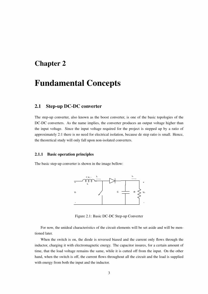
The basic step-up converter is shown in the image bellow:
-
+
Vi
-
+
VoC R
L
+ vL - iL io
Figure 2.1: Basic DC-DC Step-up Converter
For now, the unideal characteristics of the circuit elements will be set aside and will be men-
tioned later.
When the switch is on, the diode is reversed biased and the current only flows through the
inductor, charging it with electromagnetic energy. The capacitor insures, for a certain amount of
time, that the load voltage remains the same, while it is cutted off from the input. On the other
hand, when the switch is off, the current flows throughout all the circuit and the load is supplied
with energy from both the input and the inductor.
3

4 Fundamental Concepts
-
+
Vi
-
+
VoC R
L
+ vL - iL io
-
+
Vi
-
+
VoC R
L
+ vL - iL io
(a) (b)
Figure 2.2: Step-up Converter: (a) Switch on; (b) Switch off.
The process described above represents the basic principle of operation of the step-up con-
verter. However, to obtain the desired voltage level at the output is necessary to properly control
the switching frequency of the converter. Hence, the output voltage will depend on the duty cycle
of the switch. The duty cycle also defines the conduction mode of the converter.
2.1.1.1 Continuous Conduction Mode
In this mode of conduction, the current flows continuously never reaching zero. When the switch
is on the inductor voltage is given by
vL =Vi (2.1)
and when the switch is off is given by
vL =Vi−Vo (2.2)
With this information it is possible to draw the inductor voltage waveform.
vL(t)
Vi
Vi - Vo
0 t
ton toffton
Ts
Figure 2.3: Continuous Conductions Mode: Inductor voltage.
In steady state, the time integral of the inductor voltage over one switching period must be
zero [2]. So, considering the results provided by equations 2.1 and 2.2 yields
∫ Ts
0vLdt = 0

2.1 Step-up DC-DC converter 5
ViTsD+(Vi−Vo)Ts(1−D) = 0 (2.3)
where Ts = ton + to f f is the switching period and D is the duty cycle of the switch. The
rearrangement of equation 2.3 will result in the following
Vo
Vi=
11−D
= M(D) (2.4)
where M(D) is the voltage conversion ratio of the converter. The plot of equation 2.4 is shown
in the following image:
Figure 2.4: Voltage conversion ratio of an ideal DC-DC step-up converter [4].
Analysing figure 2.4 it is possible to see that the output voltage decreases with the increase of
D. So, ideally, the output voltage tends to infinity when D approaches 1. This means that the ideal
boost converter can produce any output voltage greater than the input voltage. However, due to
the non-ideal characteristics of real converters there is a limit to the output voltage [4].
Since no power losses are considered in the present analysis, the relation between the input
and output DC currents can be found.
Pi = Po⇐⇒ViIi =VoIo
Io
Ii= 1−D =
1M(D)
(2.5)
When the duty-cycle approaches 1, the output current tends to zero. This behaviour is expected,
since an output voltage increase leads to a current decrease in order to conserve the input power.
Equations 2.4 and 2.5 shows that, in this operation mode, the load has no influence on the
output current and voltage. They are only a function of the duty-cycle.
Now, lets analyse the ripple in the inductor current. Considering equations 2.1 and 2.2 it is
possible to calculate the slope of the current, which is ViL and Vi−Vo
L during ton and to f f respectively.
The current waveform is shown in figure 2.5.
According to figure 2.5, the ripple of the current can be given by
2∆iL(t) =Vi
Lton =
Vi
LDTs
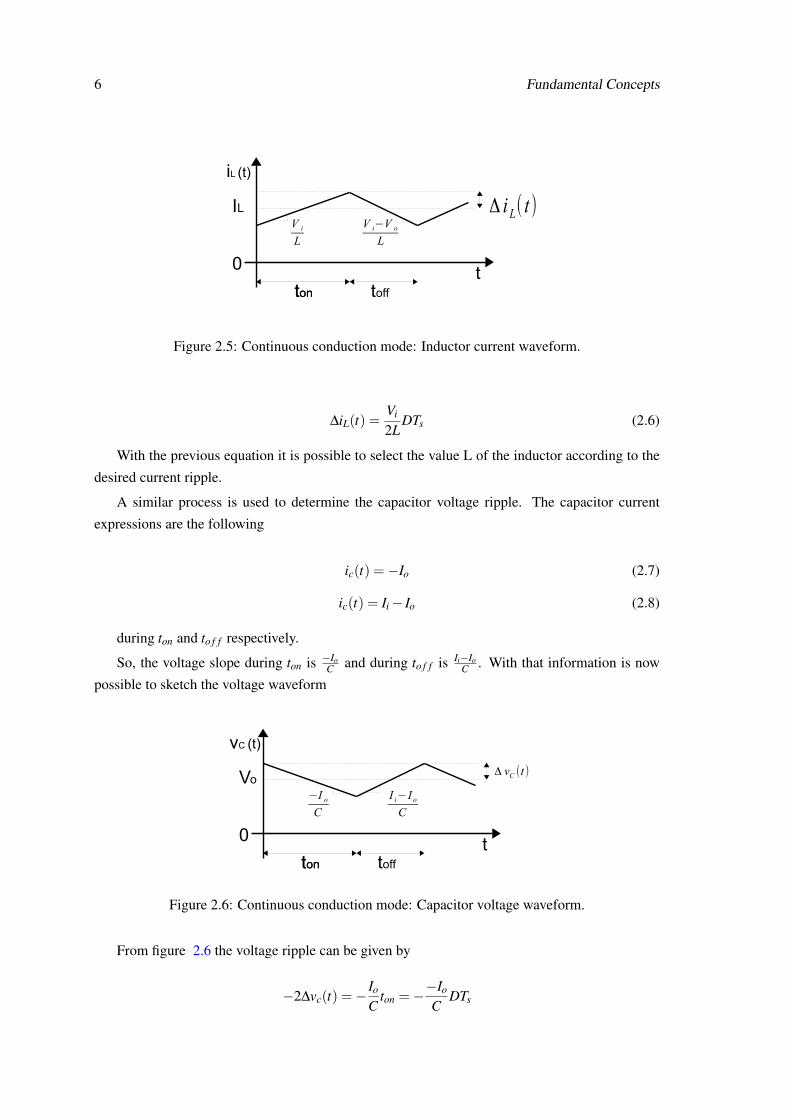
6 Fundamental Concepts
iL (t)
0 tton toffton
IL Δ i L( t)V i
L
V i−V o
L
Figure 2.5: Continuous conduction mode: Inductor current waveform.
∆iL(t) =Vi
2LDTs (2.6)
With the previous equation it is possible to select the value L of the inductor according to the
desired current ripple.
A similar process is used to determine the capacitor voltage ripple. The capacitor current
expressions are the following
ic(t) =−Io (2.7)
ic(t) = Ii− Io (2.8)
during ton and to f f respectively.
So, the voltage slope during ton is −IoC and during to f f is Ii−Io
C . With that information is now
possible to sketch the voltage waveform
vC (t)
0 tton toffton
VoΔ vC (t)
−I oC
I i−I oC
Figure 2.6: Continuous conduction mode: Capacitor voltage waveform.
From figure 2.6 the voltage ripple can be given by
−2∆vc(t) =−Io
Cton =−
−Io
CDTs

2.1 Step-up DC-DC converter 7
hlSince we are dealing with voltage conversions, it is more appropriate to define de voltage
ripple as a function of the output voltage
−2∆vc(t) =−Vo
RCDTs
∆vc(t) =−Vo
2RCDTs (2.9)
Although the output voltage is not load dependent, it can be seen from the previous equations
that the voltage ripple is. Using these equations it is possible to choose de C value of the capacitor.
Usually large capacitors are chosen in order to minimize the output ripple [4].
2.1.1.2 Discontinuous Conduction Mode
This conduction mode frequently occurs in converters operating at light load or with no load at all.
The analysis of this conduction mode is important because the properties of the converter suffer
considerable changes. For instance, the voltage conversion ratio becomes load dependent and
therefore the output voltage ceases to be only a function of the duty-cycle and the input voltage.
In the discontinuous conduction mode the inductor current reaches zero at the end of each
switching cycle (iL(t)≥ 0), as well as the inductor voltage. The equations of the inductor for this
conduction mode are the same as the equations described in section 2.1.1.1, but since the inductor
is allowed to fully discharge, the waveforms are slightly different
vL(t)
Vi
Vi - Vo
0 t
iL (t)
0 t
ton toff
Ts
ILΔ iL( t)
V i
LV i−V o
L
Δ t 1 Δ t 2
DTs DTs Δ t 1 Δ t 2
(a) (b)
Figure 2.7: Discontinuous conduction mode: Inductor voltage (a) and current (b) waveforms.
According to the inductor voltage waveform the voltage conversion ratio is given by
DVi +∆t1(Vi−Vo)+∆t3(0) = 0
Vo
Vi=
D+∆t1∆t1
(2.10)
Since ∆t1 is unknown and the voltage should be represented only as a function of D, it is
necessary to calculate the value of ∆t1.

8 Fundamental Concepts
iD(t)
I D
DT s Δ t 1 Δ t 2t
V i−V o
L
Figure 2.8: Discontinuous conduction mode: Diode current waveform.
The diode current is identical to the inductor current during to f f . Hence, the peak current of
the diode is the same as the inductor and is given by
ipk =Vi
LDTs (2.11)
The DC component of the diode current is
1Ts
∫ Ts
0iD(t)dt
which is the same as the area of figure 2.8 divided by Ts
ID =DTs(0)+
∆t1Tsipk2 +∆t2Ts(0)Ts
=∆t1ipk
2
ID =Vi
2LD∆t1Ts (2.12)
Substituting ID by the load current Io yields
Vi
2LD∆t1Ts =
Vo
R(2.13)
Vo
Vi=
RD∆t1Ts
2L
Replacing VoVi
by equation 2.10
RD∆t1Ts
2L=
D+∆t1∆t1
∆t1 = DVi
Vo−Vi(2.14)

2.1 Step-up DC-DC converter 9
Replacing this result in equation 2.13 yields
V 2o −VoVi−
V 2i D2
K= 0
where
K =2LRTs
(2.15)
Solving the quadratic equation it is possible to determine de voltage conversion ratio
Vo
Vi=
1+√
1+ 4D2
K
2= M(D,K) (2.16)
.
This equation is valid for K < Kcrit [4]. Kcrit represents the boundary between the continuous
and discontinuous conduction mode and will determined in the next section.
Now lets analyse the inductor current ripple and the capacitor voltage ripple in the discontin-
uous conduction mode. According to figure 2.7, the inductor current ripple is given by
2∆iL(t) =Vi
Lton =
Vi
LDTs
∆iL(t) =Vi
2LDTs (2.17)
The capacitor waveforms are shown in figure 2.9
ic(t)
Ii - I
o
0 t
vc(t)
0t
ton toff
Ts
Vo
Δ vC (t)
Δ t1 Δ t2DTs
DTs
(a) (b)
- Io
−I oC
Δ t1 Δ t2
Figure 2.9: Discontinuous conduction mode: Capacitor voltage(a) and current(b) waveforms.
2.1.1.3 Boundary between the continuous and discontinuous conduction mode
From the previous sections was shown that
IL > ∆iL for CCM (2.18)
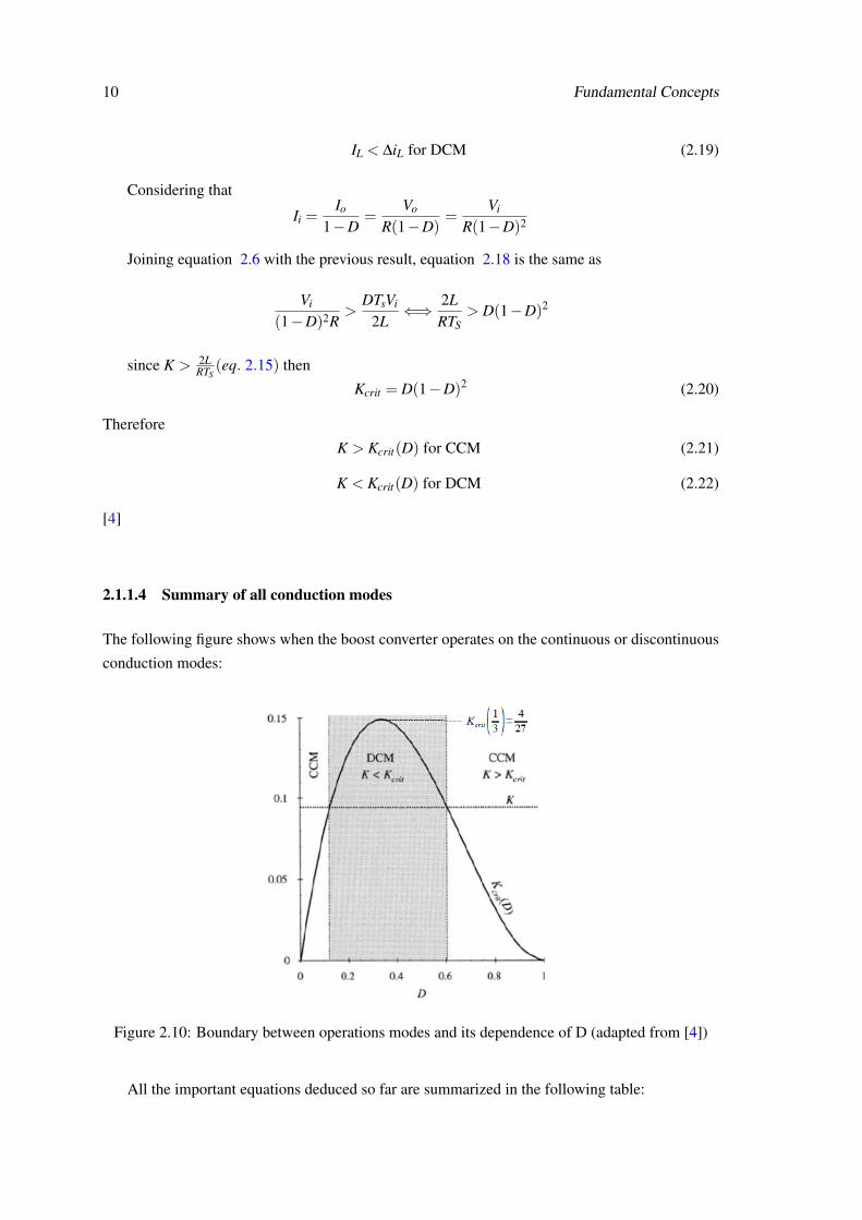
10 Fundamental Concepts
IL < ∆iL for DCM (2.19)
Considering that
Ii =Io
1−D=
Vo
R(1−D)=
Vi
R(1−D)2
Joining equation 2.6 with the previous result, equation 2.18 is the same as
Vi
(1−D)2R>
DTsVi
2L⇐⇒ 2L
RTS> D(1−D)2
since K > 2LRTS
(eq. 2.15) then
Kcrit = D(1−D)2 (2.20)
Therefore
K > Kcrit(D) for CCM (2.21)
K < Kcrit(D) for DCM (2.22)
[4]
2.1.1.4 Summary of all conduction modes
The following figure shows when the boost converter operates on the continuous or discontinuous
conduction modes:
Figure 2.10: Boundary between operations modes and its dependence of D (adapted from [4])
All the important equations deduced so far are summarized in the following table:

2.2 Control techniques 11
Table 2.1: Summary of the step-up converter conduction modes characteristics.
Conduction Mode M conditionContinuous 1
1−D K > Kcrit
Discontinuous1+
√1+ 4D2
K2 K < Kcrit
With K > 2LRTS
and Kcrit = D(1−D)2
2.2 Control techniques
2.2.1 Classic PWM control
This is a closed loop method which controls the output voltage by employing a constant switch-
ing frequency, varying only the duty-cycle. There are other methods that use variable switching
frequency, but becomes difficult to filter the ripple of the converter waveforms. The basic block
diagram of the converter and the controller is shown in the figure bellow.
DC-DC step-up
converterV in
f s
+
Sawtooth Generator
Control Signal
+-
Comparator
vcontrol
V out (measured )
V out (desired )-PI
Figure 2.11: Closed loop PWM control block diagram.
The control signal is generated by comparing the control voltage (vcontrol) with the sawtooth
wave. Since the rate of change of vcontrol is very large compared with the frequency of the sawtooth
wave, locally it can be considered constant.
The basic operation principle is very simple: when the control voltage is greater than the
sawtooth waveform, the control signal becomes high, making the switch turn on. On the other
hand, when the control voltage is smaller than the sawtooth waveform, the switch is turned off.
The switching frequency and the duty-cycle are given by

12 Fundamental Concepts
t
vcontrol
on
off
Vst
Vst (t)
ton
toff T
s
Vcontrol
> Vst (t)
Vcontrol
< Vst (t)
Figure 2.12: PWM: Control signal waveform.
fs =1Ts
(2.23)
D =ton
Ts=
vcontrol
V̂st(2.24)
where V̂st is the peak voltage of the sawtooth waveform.
As indicated in figure 2.12 the switching frequency is imposed by the frequency of the saw-
tooth waveform. Since DC-DC converters have two conduction modes, as covered in sections
2.1.1.1 and 2.1.1.2, the control and the converter itself should by design considering those modes
of operation [2].
2.3 Semiconductor devices
The controlled flow of charged particles is fundamental to the operation of all electronic devices.
The material used in these devices must be capable of providing a source of mobile charges and
the processes witch govern the flow of charges must be amenable to control. Germanium and
gallium are widely used semiconductors, however silicon is the most predominant.
The crystal structure of silicon consists of a regular repetition in three dimensions of a unit cell
having the form of a tetrahedron with an atom at each vertex like the one shown on figure 2.13.
But, for simplicity, the unit cell is often represented in 2D, as shown in figure 2.14(a). Silicon has
a total of 14 electrons in its atomic structure, 4 of which are valence electrons. The inert ionic core
has a charge of +4. The valence electrons serve to bind one atom to the next.
At certain temperatures the covalent bonds are broken and the electrons are free to wander
randomly throughout the crystal. The absence of the electron in the covalent bond is called a hole.
When a hole exists it is relatively easy for a valence electron in a neighbouring atom to leave its
covalent bond to fill this hole. An electron moving from a bond to fill a hole leaves another hole
in its initial position. This hole may now be filled by an electron from another covalent bond, and

2.3 Semiconductor devices 13
Figure 2.13: Silicon single-crystal structure (based on [5]).
the hole will correspondingly "move" one more step in the opposite direction to the motion of the
electron. When an electromagnetic field is applied, the electron motion is no longer random and
becomes organized.
If the crystal structure is a pure sample of silicon and has no foreign atoms, such pure crystal
is called an intrinsic semiconductor. Consequently, the hole concentration p and the electron
concentration n must be equal and the intrinsic concentration ni, which is temperature-dependent,
is given by ni = p = n.
When the crystal has impurities in its structure, the semiconductor is called extrinsic or doped.
The addition of impurities is a common expedient used to increase the number of carriers. A
small, carefully controlled, impurity content is introduced in an intrinsic semiconductor. Each
type of impurity establishes a semiconductor which as a predominance of one kind of carrier. The
usual level of doping is in the range of 1 impurity atom for 106 to 108 silicon atoms. So, most
physical and chemical properties are essentially those of silicon and only the electrical properties
change.
When an intrinsic semiconductor is doped with pentavalent impurities (called donors), such
as antimony, phosphorus or arsenic, the number of electrons increases and the number of holes
decreases. Consequently, the dominant carriers are the negative electrons witch results in an n-
type semiconductor (figure 2.14(b)). On the other hand, when an intrinsic semiconductor is doped
with trivalent impurities (called acceptors), such as boron, gallium or indium, the electrons only fill
three covalent bonds. The void that exists in the fourth bond constitutes a hole. Thus, the dominant
carriers are the holes and this type of crystal is called p-type semiconductor (figure 2.14(c)) [6].
Semiconductor devices are electrical devices constituted with semiconductor material. Each
device type has different combinations of n and p layers that provide unique electrical characteris-
tics. Examples of commonly used semiconductor devices are the diode, transistor or the thyristor.
2.3.1 Diode
The diode is a non linear element since there is no direct relation between the current and the
voltage applied to its terminals. The diode symbol is shown in figure 2.15.
The positive and negative terminals are called anode (A) and cathode (C) respectively. Ideally,
the diode behaviour is very simple. When a positive voltage is applied the diode becomes directly
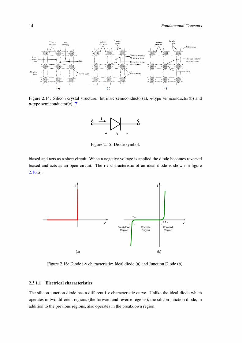
14 Fundamental Concepts
Figure 2.14: Silicon crystal structure: Intrinsic semiconductor(a), n-type semiconductor(b) andp-type semiconductor(c) [7].
i
+ v -
A C
Figure 2.15: Diode symbol.
biased and acts as a short circuit. When a negative voltage is applied the diode becomes reversed
biased and acts as an open circuit. The i-v characteristic of an ideal diode is shown in figure
2.16(a).
i
vForwardRegion
ReverseRegion
BreakdownRegion
0,7 V
−V ZK
i
v
(a) (b)
Figure 2.16: Diode i-v characteristic: Ideal diode (a) and Junction Diode (b).
2.3.1.1 Electrical characteristics
The silicon junction diode has a different i-v characteristic curve. Unlike the ideal diode which
operates in two different regions (the forward and reverse regions), the silicon junction diode, in
addition to the previous regions, also operates in the breakdown region.

2.3 Semiconductor devices 15
The forward region of operation occurs when v > 0. The i-v curve can be approximated by the
following expression
i = IS(ev
nVT −1) (2.25)
where Is is the saturation current and n is a constant value between 1 and 2, according to the
material and physical structure of the diode. VT is the thermal voltage which is given by
VT =kTq
(2.26)
where k is the Boltzman’s constant, q the magnitude of the electric charge and T is the absolute
temperature.
If i >> IS, i can be approximated by
i = ISev
nVT (2.27)
Analysing the forward region in figure 2.16 (b), for v < 0.5V the current is very close to zero.
When the diode is fully conducting, the voltage drop is approximately between 0.6 and 0.8 V.
Hence, usually is assumed that the voltage drop of a fully conducting diode is 0.7 V.
The reverse region of operation occurs when v < 0, and the diode current is given by
i≈−IS (2.28)
Ideally, the diode in this region should have i = 0. However, due to leakage effects, a reverse
current flows trough the diode. Both IS and the reverse current are proportional to the junction
area, but IS doubles with every 5oC rise and the reverse current doubles with every 10oC rise.
The reverse region of operation occurs when the breakdown voltage, VZK , of the diode is
exceeded
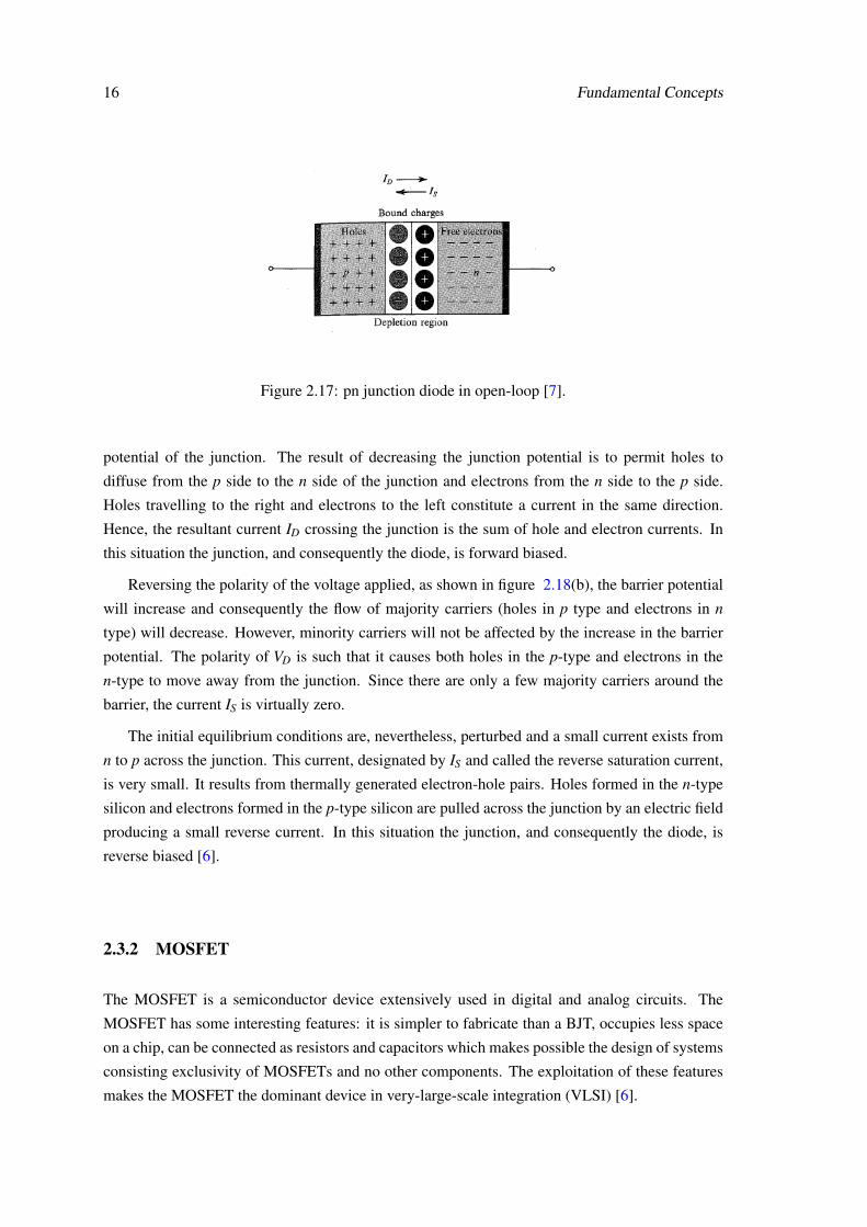
2.3.1.2 Physical operation
The pn junction is the basic block on which the operation of all semiconductor devices depends.
If two metal terminals are added, the pn junction is itself a semiconductor device - the junction
diode.
A pn junction is formed when a single crystal of semiconductor is doped with acceptors on
one side and donors on the other as shown in figure 2.17. It is assumed that the junction has
reached equilibrium conditions and that the semiconductor has uniform cross section. Initially, a
concentration gradient exists across the junction, causing holes to diffuse to the right and electrons
to the left. Near the junction there are neutralized ions. Since this region depletes of mobile
charges it is called depletion region.
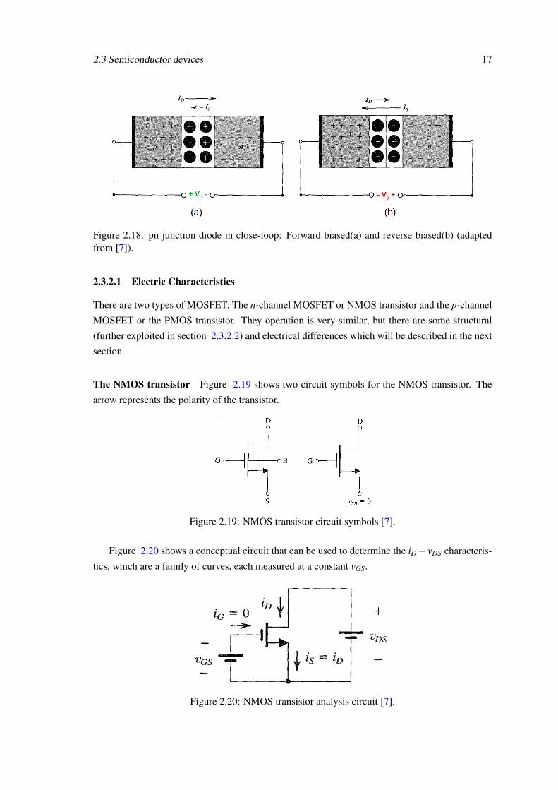
In figure 2.18(a) the VD voltage is applied to the junction with the positive terminal connected
to the p side and the negative terminal to the n side. Assuming that there is no voltage drop on
the metal terminals and outside the depletion region, the applied voltage VD reduces the barrier
16 Fundamental Concepts
Figure 2.17: pn junction diode in open-loop [7].
potential of the junction. The result of decreasing the junction potential is to permit holes to
diffuse from the p side to the n side of the junction and electrons from the n side to the p side.
Holes travelling to the right and electrons to the left constitute a current in the same direction.
Hence, the resultant current ID crossing the junction is the sum of hole and electron currents. In
this situation the junction, and consequently the diode, is forward biased.
Reversing the polarity of the voltage applied, as shown in figure 2.18(b), the barrier potential
will increase and consequently the flow of majority carriers (holes in p type and electrons in n
type) will decrease. However, minority carriers will not be affected by the increase in the barrier
potential. The polarity of VD is such that it causes both holes in the p-type and electrons in the
n-type to move away from the junction. Since there are only a few majority carriers around the
barrier, the current IS is virtually zero.
The initial equilibrium conditions are, nevertheless, perturbed and a small current exists from
n to p across the junction. This current, designated by IS and called the reverse saturation current,
is very small. It results from thermally generated electron-hole pairs. Holes formed in the n-type
silicon and electrons formed in the p-type silicon are pulled across the junction by an electric field
producing a small reverse current. In this situation the junction, and consequently the diode, is
reverse biased [6].
2.3.2 MOSFET
The MOSFET is a semiconductor device extensively used in digital and analog circuits. The
MOSFET has some interesting features: it is simpler to fabricate than a BJT, occupies less space
on a chip, can be connected as resistors and capacitors which makes possible the design of systems
consisting exclusivity of MOSFETs and no other components. The exploitation of these features
makes the MOSFET the dominant device in very-large-scale integration (VLSI) [6].
2.3 Semiconductor devices 17
Figure 2.18: pn junction diode in close-loop: Forward biased(a) and reverse biased(b) (adaptedfrom [7]).
2.3.2.1 Electric Characteristics
There are two types of MOSFET: The n-channel MOSFET or NMOS transistor and the p-channel
MOSFET or the PMOS transistor. They operation is very similar, but there are some structural
(further exploited in section 2.3.2.2) and electrical differences which will be described in the next
section.
The NMOS transistor Figure 2.19 shows two circuit symbols for the NMOS transistor. The
arrow represents the polarity of the transistor.
Figure 2.19: NMOS transistor circuit symbols [7].
Figure 2.20 shows a conceptual circuit that can be used to determine the iD−vDS characteris-
tics, which are a family of curves, each measured at a constant vGS.
Figure 2.20: NMOS transistor analysis circuit [7].

18 Fundamental Concepts
The characteristic curves shown in figure 2.21 indicate that are three distinct regions of opera-
tion: the cutoff, the triode and the saturation region. The saturation region is used ifif the MOSFET
is to operate as an amplifier. For operation as a switch, the cutoff and triode regions are utilized
[7].
Triode region Saturation regioniD
vDS
vDS⩽vGS−V tvDS⩾vGS−V t
vDS=vGS−V t
vGS=V t+2.0
vGS=V t+1.5
vGS=V t+1.0
vGS=V t+0.5
vGS⩽V t (cuttoff)
Figure 2.21: NMOS transistor: the iD− vDS characteristic (based on [7]).
Cutoff region The device is cut off when vGS < Vt , where Vt is the threshold voltage of the
MOSFET. In this case, Vt is a positive voltage. [7].
Triode region To operate the MOSFET in the triode region first is necessary to induce a
channel vGS ≤ Vt and the keep vDS small enough so that the channel remains continuous. This is
achieved by ensuring that vGS− vDS >Vt .
In the triode region, the iD−vDS characteristic can be described by the following relationship:
iD = Kn[(vGS− vDS)vDS−12
vDS2] (2.29)
Where Kn is a value determined by the fabrication technology [7].
Saturation region To operate the MOSFET in the saturation region, a channel must be in-
duced by making vGS ≥Vt and pinched off at the drain end by raising vDS to a value that results in
vDS ≥ vGS−Vt .
The boundary between the triode region and the saturation region is characterized by vDS =
vGS−Vt . Substituting the value of vDS into equation 2.29 results in the saturation value of the
curren iD

2.3 Semiconductor devices 19
iD =12
Kn(vGS−Vt)2 (2.30)
Thus, in saturation, the MOSFET provides a drain current whose value is independent of the
drain voltage vDS and is determined by the gate voltage [7].
The PMOS transistor Figure 2.22 shows two circuit symbols for the PMOS transistor. Once
again, the arrow represents the polarity of the transistor. For the p-channel device, the threshold
voltage Vt is negative
Figure 2.22: PMOS transistor circuit symbols [7].
Figure 2.23 shows a conceptual circuit that can be used to determine the iD−vDS characteris-
tics.
Figure 2.23: PMOS transistor analysis circuit [7].
Triode region To induce a channel it is necessary to make vGS ≥ |Vt | and apply a drain
voltage vDS ≥ vGS−Vt . The iD current is given by [7]:
iD = Kp[(vGS− vDS)vDS−12
vDS2] (2.31)
Saturation region To operate the MOSFET in the saturation region, vDS must satisfy the
relationship vDS ≤ vGS−Vt . The current is given by
iD =12
Kp(vGS−Vt)2 (2.32)
Where Kp is a value determined by the fabrication technology [7].
20 Fundamental Concepts
2.3.2.2 Physical operation
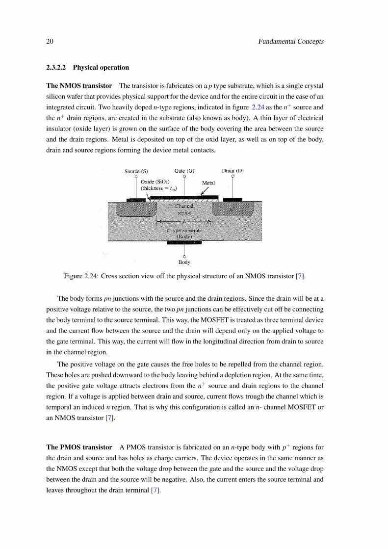
The NMOS transistor The transistor is fabricates on a p type substrate, which is a single crystal
silicon wafer that provides physical support for the device and for the entire circuit in the case of an
integrated circuit. Two heavily doped n-type regions, indicated in figure 2.24 as the n+ source and
the n+ drain regions, are created in the substrate (also known as body). A thin layer of electrical
insulator (oxide layer) is grown on the surface of the body covering the area between the source
and the drain regions. Metal is deposited on top of the oxid layer, as well as on top of the body,
drain and source regions forming the device metal contacts.
Figure 2.24: Cross section view off the physical structure of an NMOS transistor [7].
The body forms pn junctions with the source and the drain regions. Since the drain will be at a
positive voltage relative to the source, the two pn junctions can be effectively cut off be connecting
the body terminal to the source terminal. This way, the MOSFET is treated as three terminal device
and the current flow between the source and the drain will depend only on the applied voltage to
the gate terminal. This way, the current will flow in the longitudinal direction from drain to source
in the channel region.
The positive voltage on the gate causes the free holes to be repelled from the channel region.
These holes are pushed downward to the body leaving behind a depletion region. At the same time,
the positive gate voltage attracts electrons from the n+ source and drain regions to the channel
region. If a voltage is applied between drain and source, current flows trough the channel which is
temporal an induced n region. That is why this configuration is called an n- channel MOSFET or
an NMOS transistor [7].
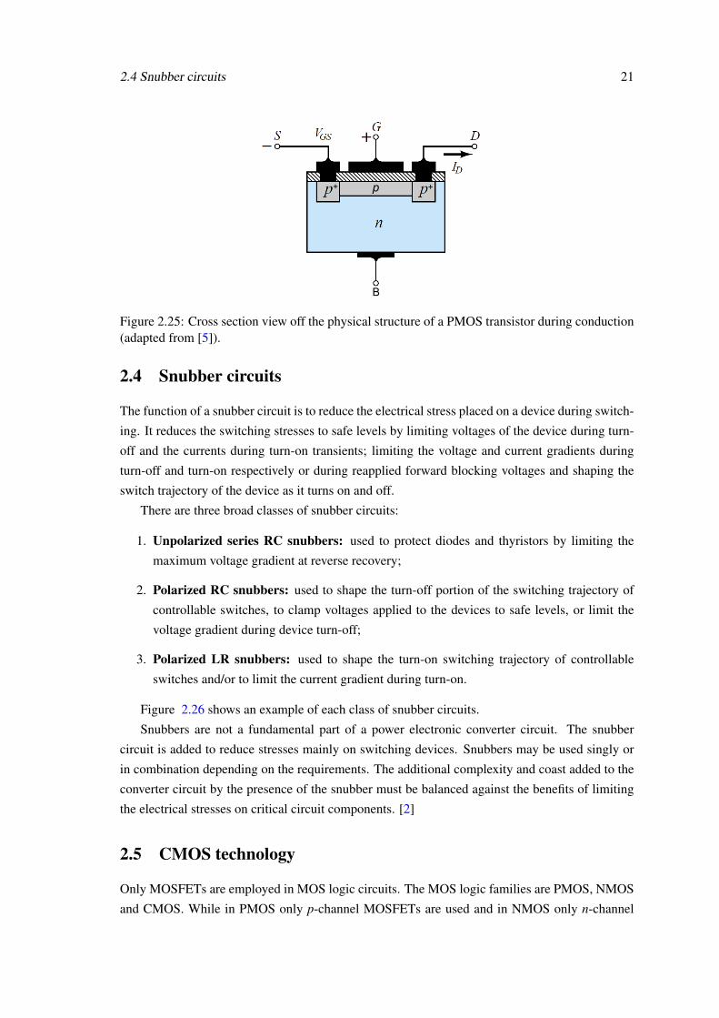
The PMOS transistor A PMOS transistor is fabricated on an n-type body with p+ regions for
the drain and source and has holes as charge carriers. The device operates in the same manner as
the NMOS except that both the voltage drop between the gate and the source and the voltage drop
between the drain and the source will be negative. Also, the current enters the source terminal and
leaves throughout the drain terminal [7].
2.4 Snubber circuits 21
B
+ +p
Figure 2.25: Cross section view off the physical structure of a PMOS transistor during conduction(adapted from [5]).
2.4 Snubber circuits
The function of a snubber circuit is to reduce the electrical stress placed on a device during switch-
ing. It reduces the switching stresses to safe levels by limiting voltages of the device during turn-
off and the currents during turn-on transients; limiting the voltage and current gradients during
turn-off and turn-on respectively or during reapplied forward blocking voltages and shaping the
switch trajectory of the device as it turns on and off.
There are three broad classes of snubber circuits:
1. Unpolarized series RC snubbers: used to protect diodes and thyristors by limiting the
maximum voltage gradient at reverse recovery;
2. Polarized RC snubbers: used to shape the turn-off portion of the switching trajectory of
controllable switches, to clamp voltages applied to the devices to safe levels, or limit the
voltage gradient during device turn-off;
3. Polarized LR snubbers: used to shape the turn-on switching trajectory of controllable
switches and/or to limit the current gradient during turn-on.
Figure 2.26 shows an example of each class of snubber circuits.
Snubbers are not a fundamental part of a power electronic converter circuit. The snubber
circuit is added to reduce stresses mainly on switching devices. Snubbers may be used singly or
in combination depending on the requirements. The additional complexity and coast added to the
converter circuit by the presence of the snubber must be balanced against the benefits of limiting
the electrical stresses on critical circuit components. [2]
2.5 CMOS technology
Only MOSFETs are employed in MOS logic circuits. The MOS logic families are PMOS, NMOS
and CMOS. While in PMOS only p-channel MOSFETs are used and in NMOS only n-channel
22 Fundamental Concepts
(a) (b) (c)
Figure 2.26: Examples of snubber circuits: diode snubber(a), transistor turn-on snubber(b) andtransistor turn-off snubber(c) (adapded from [2])
MOSFETs are used, in CMOS, both p and n-channel MOSFETs are employed and are fabricated
on the same silicon chip. The power dissipation is extremely small for CMOS and hence CMOS
logic has become very popular.
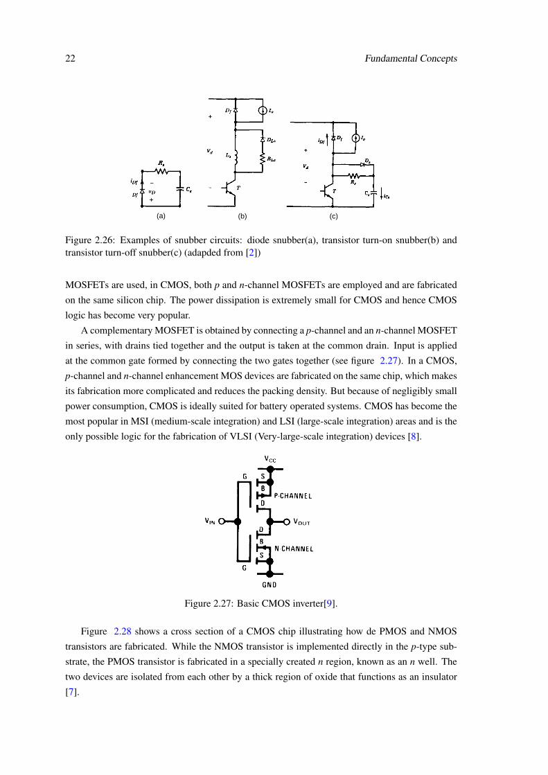
A complementary MOSFET is obtained by connecting a p-channel and an n-channel MOSFET
in series, with drains tied together and the output is taken at the common drain. Input is applied
at the common gate formed by connecting the two gates together (see figure 2.27). In a CMOS,
p-channel and n-channel enhancement MOS devices are fabricated on the same chip, which makes
its fabrication more complicated and reduces the packing density. But because of negligibly small
power consumption, CMOS is ideally suited for battery operated systems. CMOS has become the
most popular in MSI (medium-scale integration) and LSI (large-scale integration) areas and is the
only possible logic for the fabrication of VLSI (Very-large-scale integration) devices [8].
Figure 2.27: Basic CMOS inverter[9].
Figure 2.28 shows a cross section of a CMOS chip illustrating how de PMOS and NMOS
transistors are fabricated. While the NMOS transistor is implemented directly in the p-type sub-
strate, the PMOS transistor is fabricated in a specially created n region, known as an n well. The
two devices are isolated from each other by a thick region of oxide that functions as an insulator
[7].
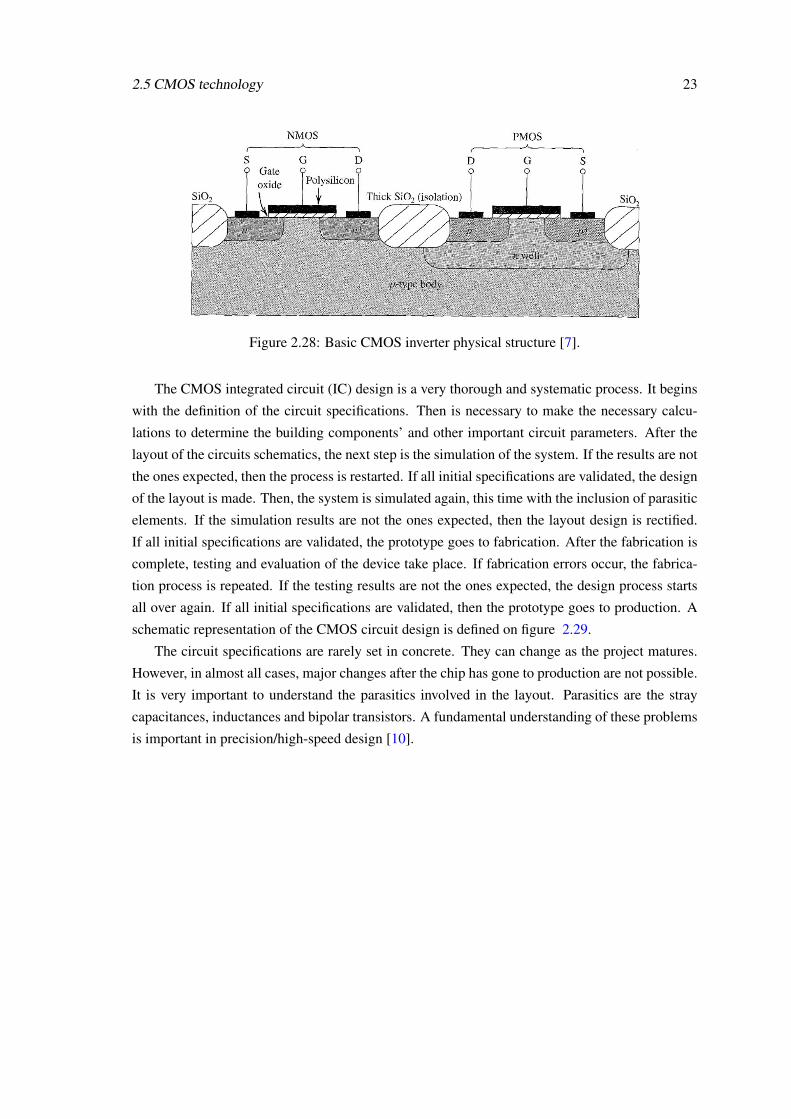
2.5 CMOS technology 23
Figure 2.28: Basic CMOS inverter physical structure [7].
The CMOS integrated circuit (IC) design is a very thorough and systematic process. It begins
with the definition of the circuit specifications. Then is necessary to make the necessary calcu-
lations to determine the building components’ and other important circuit parameters. After the
layout of the circuits schematics, the next step is the simulation of the system. If the results are not
the ones expected, then the process is restarted. If all initial specifications are validated, the design
of the layout is made. Then, the system is simulated again, this time with the inclusion of parasitic
elements. If the simulation results are not the ones expected, then the layout design is rectified.
If all initial specifications are validated, the prototype goes to fabrication. After the fabrication is
complete, testing and evaluation of the device take place. If fabrication errors occur, the fabrica-
tion process is repeated. If the testing results are not the ones expected, the design process starts
all over again. If all initial specifications are validated, then the prototype goes to production. A
schematic representation of the CMOS circuit design is defined on figure 2.29.
The circuit specifications are rarely set in concrete. They can change as the project matures.
However, in almost all cases, major changes after the chip has gone to production are not possible.
It is very important to understand the parasitics involved in the layout. Parasitics are the stray
capacitances, inductances and bipolar transistors. A fundamental understanding of these problems
is important in precision/high-speed design [10].

24 Fundamental Concepts
Define circuit inputsand outputs
(circuit specifications)
Calculations and
schematics
Circuit simulations
Does the circuit Meet specs?
Layout
Re-simulate with parasitics
Does the circuit meet specs?
Prototype fabrication
Testing and evaluation
Does the circuit meet specs?
Production
No
Yes
No
Yes
No, fabrication problem
Yes
No, specs problem
Figure 2.29: CMOS IC design process (based on [10]).
Chapter 3
State of the Art
3.1 Step-up DC-DC converter: More advanced solutions
The DC-DC step-up converter described in chapter 2 represents the classical configuration of the
topology. Despite of the fact that this configuration is sufficient for a wide number of applications,
there are other configurations more efficient or that overcome some of the faults of the classical
configuration and, therefore, are more suitable for high performance applications.
For instance, the transfer function of the classic configuration of the DC-DC step-up converter
has a zero on the right-half plane (RHP) of the s plane Thus it is a non-minimum phase system,
which means that it has a larger phase component leading to a slower dynamic response. To
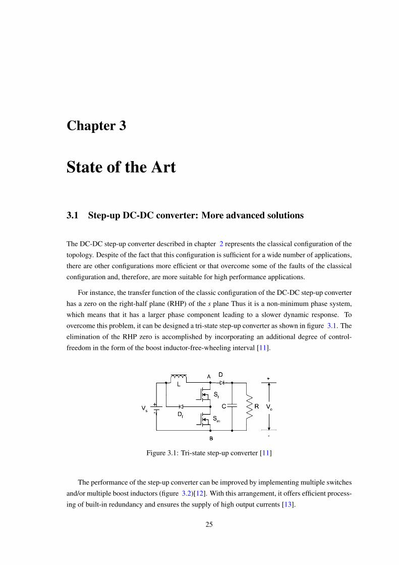
overcome this problem, it can be designed a tri-state step-up converter as shown in figure 3.1. The
elimination of the RHP zero is accomplished by incorporating an additional degree of control-
freedom in the form of the boost inductor-free-wheeling interval [11].
Figure 3.1: Tri-state step-up converter [11]
The performance of the step-up converter can be improved by implementing multiple switches
and/or multiple boost inductors (figure 3.2)[12]. With this arrangement, it offers efficient process-
ing of built-in redundancy and ensures the supply of high output currents [13].
25

26 State of the Art
Figure 3.2: Step-up converter with multiple switches and inductors [13]
3.2 Design of integrated DC-DC converters with CMOS technology
Since the diode, resistors and capacitances can be accomplished by MOSFETs, the converter can
be mostly implemented on chip, except for the inductor which has to be connected externally.
Inductors can actually be implemented on chip, but that is not feasible for the inductance values
required in these applications. However, there are other advantages that result from the implemen-
tation of DC-DC converters with CMOS technology.
Two important characteristics of the CMOS technology are high noise immunity and low static
power consumption. Significant power is only drawn when the transistors are switching between
on and off states. Consequently, MOS circuitry dissipates less power and is denser than other im-
plementations having the same functionality. Since low voltage power MOSFETs implemented in
a deep submicron CMOS process exhibit much shorter switching delays than those in conventional
power MOSFETs, this allows the CMOS devices to operate in the MHz range for high-efficient
mobile applications. As the switching frequency of power converters continues to increase, both
switching and gate-drive power losses start to limit the efficiency of output power stage. Par-
ticularly, conventional vertical power MOSFETs have relatively large gate to drain overlap area.
This introduces a significant switching delay since a large input capacitance requires more charg-
ing and discharging time for each turn on and off transition of a power MOSFET. On the other
hand, CMOS-based power MOSFETs have much smaller input gate capacitance due to smaller
gate-drain/source overlap capacitance, gate oxide capacitance and parasitic fringing capacitance.
Nevertheless, one of the drawbacks is that more advanced CMOS technology is accompanied
with larger parasitic interconnect resistances and capacitances. Without any processing and device
structural changes, performance improvement can be only gained by introducing a new layout
structure. Some of the possible layout structures are: Multi-Finger and Regular Waffle layout
[14].
3.3 Existing control techniques 27
3.3 Existing control techniques
Any DC to DC converter will be designed for specific input voltage and output conditions. In other
words, the circuit will be operated at steady state condition only. But in practice this may not be
possible and there is always a possibility of some disturbances which cause the circuit operation to
deviate from the nominal values considerably. These disturbances may be due to the changes in the
source, load, circuit parameters, and perturbation in switching time and events such as start up and
shut down. This deviation of the circuit operation from the desired nominal behaviour is known as
the dynamic behaviour of the circuit. If the above mentioned disturbances have negligible effect
on the circuit operation, no action will be required by the designer to correct this situation. But
in most cases the departure from nominal conditions will affect the circuit operations to large
extent and therefore, the designers will be required to design a proper controller or compensator
to overcome this situation of the circuit operation [15].
Since the step-up converter exhibits non-linear and non-minimum phase properties in the pres-
ence of uncertain loads, it is necessary to design a robust controller [16]. The control of the step-up
converter is not easy and has been a serious concern for the control theorists over the years.
3.3.1 PI and PID controllers
For control over steady state and transient errors, the control signal of a PID controller is a linear
combination of the error, the integral of the error, and the time rate of change of the error. The PID
controller contains all the control components (proportional, derivative, and integral). In order to
get acceptable performance the constants KP, KD and KI can be adjusted. This adjustment process
is called tuning the controller. Increasing KP and KI tend to reduce errors but may not be capable
of producing adequate stability. The PID controller provides both an acceptable degree of error
reduction and an acceptable stability and damping.
The integral term in a PI controller causes the steady-state error to reduce to zero, which is
not the case for proportional-only control in general. The lack of derivative action may make the
system more steady in the steady state in the case of noisy data. This is because derivative action is
more sensitive to higher-frequency terms in the inputs. Without derivative action, a PI-controlled
system is less responsive to real (non-noise) and relatively fast alterations in state and so the
system will be slower to reach set-point and slower to respond to perturbations than a well-tuned
PID system may be [15].
The drawback of this controllers is that they are nor capable of auto-adjust KP, KD or KI in
order to keep up with dynamic behaviour of the circuit. They are tuned during the design process
of the circuit and stay with the same gain values, always.
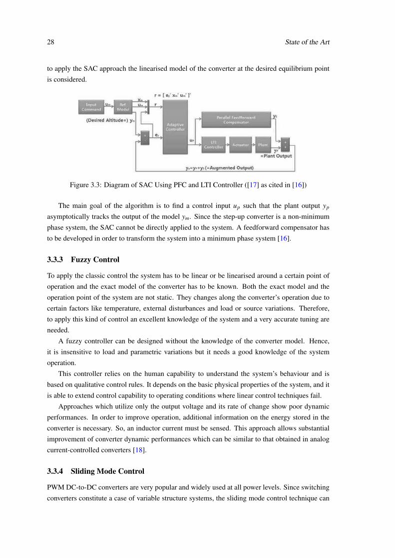
3.3.2 Simple Adaptive Control
The simple adaptive control (SAC) is an algorithm for unmodeled dynamics since the order of
reference model can be chosen almost freely regardless of that of the controlled system. In order
28 State of the Art
to apply the SAC approach the linearised model of the converter at the desired equilibrium point
is considered.
Figure 3.3: Diagram of SAC Using PFC and LTI Controller ([17] as cited in [16])
The main goal of the algorithm is to find a control input up such that the plant output yp
asymptotically tracks the output of the model ym. Since the step-up converter is a non-minimum
phase system, the SAC cannot be directly applied to the system. A feedforward compensator has
to be developed in order to transform the system into a minimum phase system [16].
3.3.3 Fuzzy Control
To apply the classic control the system has to be linear or be linearised around a certain point of
operation and the exact model of the converter has to be known. Both the exact model and the
operation point of the system are not static. They changes along the converter’s operation due to
certain factors like temperature, external disturbances and load or source variations. Therefore,
to apply this kind of control an excellent knowledge of the system and a very accurate tuning are
needed.
A fuzzy controller can be designed without the knowledge of the converter model. Hence,
it is insensitive to load and parametric variations but it needs a good knowledge of the system
operation.
This controller relies on the human capability to understand the system’s behaviour and is
based on qualitative control rules. It depends on the basic physical properties of the system, and it
is able to extend control capability to operating conditions where linear control techniques fail.
Approaches which utilize only the output voltage and its rate of change show poor dynamic
performances. In order to improve operation, additional information on the energy stored in the
converter is necessary. So, an inductor current must be sensed. This approach allows substantial
improvement of converter dynamic performances which can be similar to that obtained in analog
current-controlled converters [18].
3.3.4 Sliding Mode Control
PWM DC-to-DC converters are very popular and widely used at all power levels. Since switching
converters constitute a case of variable structure systems, the sliding mode control technique can

3.3 Existing control techniques 29
Figure 3.4: Block diagram of fuzzy control scheme of DC-DC converters [18].
be a possible option to control this kind of circuits ([19] as cited in [15]). Sliding Mode controllers
are well known for their robustness and stability. The nature of the controller is to ideally operate
at an infinite switching frequency such that the controlled variables can track a certain reference
path to achieve the desired dynamic response and steady-state operation ([20] as cited in [15]).
This requirement for operation at infinite switching frequency, however, challenges the feasibility
of applying SM controllers in power converters. This is because extreme high speed switching
in power converters results in excessive switching and inductor losses as well as electromagnetic
interference (EMI) noise issues [15].
The purpose of the switching control law is to drive the non-linear plant’s state trajectory
onto a pre-specified surface in the state space and to maintain the plant’s state trajectory for the
subsequent time. This surface is called the switching surface ([20] as cited in [15]). When the plant
trajectory is above the surface a feedback path has one gain and a different gain if the trajectory
drops below the surface. This surface defines the rule for proper switching and is called a sliding
surface (sliding manifold). Ideally, once intercepted, the switched control maintains the plant’s
state trajectory on the surface for all subsequent time and the plant’s state trajectory slides along
this surface [15].
Figure 3.5: Block diagram a sliding mode control scheme of a DC–DC converter [15].

30 State of the Art
Chapter 4
Radiation hardening technology
In the late 1990s, a group of integrated circuit suppliers wanted to serve the satellite marketplace.
Success in the marketplace hinged on the ability of these companies to radiation-harden ICs by
design using the intrinsic hardness of leading-edge wafer fabrication process technology. Suppliers
embracing the new business model adopted the title of Radiation Hardening-By-Design (RHBD)
circuit suppliers. To the industry, RHBD promised space-ready leading-edge products, ending a
decades-old trend of relying on ICs that were one or more generations behind the best-in-class
devices [21].
4.1 Design of power converters
The design of electronic circuits becomes a real challenge when considering the issue of radiation.
In power converters, parameters such as efficiency, converter output voltage, step response, loop
gain frequency response or phase margin may be affected by radiation, depending on the converter
topology [3]. Power converters may be very sensitive to radiation (total-dose, single event effects
and displacement damage) given that their radiation response is also dependent on temperature,
input bias conditions and load conditions ([22] cited in [3]).
4.2 Ionizing Radiation Effects
When ionization occurs over a short period of time, large photo-currents occur, resulting in upset
and latch-up. As a result of these photocurrents, circuits may exhibit logic-state upset due to power
supply droop sometimes called rail collapse. Photocurrent can also trigger destructive latch-up or
metal burnout. These phenomena are referred to as Dose Rate Upset and Dose Rate Latch-Up
respectively. RHBD suppliers mitigate the effects of large photo-currents by using special spatial
layout rules and techniques to limit parasitic gains [21].
Accumulated dose leads to threshold voltage shifts in CMOS devices due to trapped holes in
the oxide and the formation of interface states. It has been shown that the dominant radiation
31

32 Radiation hardening technology
effects in MOS devices are due to total ionizing dose (TID) effects, and not due to displacement
damage ([22] cited in [3]).
4.3 Alternatives to radiation hardening by design
One possible alternative is the use of redundancy in the storage element to mitigate particle strikes.
In the case of redundancy, sensitive critical nodes within flip-flops and latches are made redundant
and spaced apart to prevent a single ion from upsetting both critical nodes. The drive strengths of
transistors controlling critical nodes are also sized to reduce the effect of charged particle strikes.
Redundant circuits are larger than conventional commercial flip-flops or latches and burn more
power than minimum configuration commercial flip-flops and latches. Redundant flip-flops and
latches also pay a speed and power penalty due to the increased cell complexity and larger transis-
tors on size controlling sensitive nodes.
Another proven technique in the mitigation of charge-particle-induced upset and transients is
the use of multiple phases of the clock coupled to a majority vote circuit. Using small differences in
clock phase to create N samples of the data presented to N sequential circuits and then voting the N
outcomes effectively filters out both upsets and transient upsets in the sequential circuit. Temporal
clocking circuits are also larger, slower, and burn more power than minimum size commercial
flip-flops and latches [21].
Chapter 5
Dissertation overview
5.1 Project description
The aim of the dissertation is to design and implement a radiation hard DC-DC converter with an
input of 1.2 V and an output of 2.5 V with a current drive capability of 100 mA. The converter will
be designed on chip using CMOS technology. All components of the converter and the regulation
block will be implemented on chip with the exception of the inductor, which will be connected
externally. The converter has to be capable of withstanding harsh environmental conditions such
as high radiation levels and therefore has to be designed with radiation hard features.
5.2 Final remarks
The step-up converter Since the main goal of the project is to rise the input voltage by a small
ratio of approximately 2:1 there is no need for electrical isolation and therefore the step-up con-
verter is the most suitable choice. Yet, this type of converter has many different configurations
available, each one of them with its pros and cons. The basic configuration studied in chapter 2
is suitable for a variety of applications, but it has some drawbacks, which were previously ad-
dressed. The strategic addition of more components to the circuit such as more MOSFETs or
diodes could enhance the system performance. But the excessive addition of components, instead
of just solving the converter’s issues, it can also create further ones. Besides, since in this project
the converter has to operate in radioactive environments there are other factors to take into account
before choosing the configuration of the converter.
The converter controller Analog control of power converters is widely used and is a very com-
mon control approach to dc-dc converters. Nevertheless it has some disadvantages, such as lack
of flexibility and ability to adapt to new situations, it has a very hard and time consuming tuning
process and for more complex control configurations occupies a relatively large amount of space.
33
34 Dissertation overview
Digital control methods allow the implementation of non-linear, predictive and adaptive con-
trol. They are less susceptible to external and parametric variations. Are less sensitive to noise
and changing the controller does not require hardware modifications.
The matter of choosing between analog and digital control is always a challenge. Yet, in a
regular application, if efficiency and high performance are a priority and the application requires
high control complexity, the digital control is often the first choice. Once again, due to the radiation
hardening features required for the converter, there are other factors to take into account before
choosing the control type.
Radiation considerations Digital controllers have to be implemented on a microprocessor or on
a more advanced variant, like a digital signal processor (DSP). Thereby digital control is suscep-
tible to radiation effects since the internal logic values can be inconveniently modified. A bit-flip
can produce a temporary or more permanent damage that may require the reset of the system. For
instance, a bit-flip could change critical data or disturb severely the operation of the processor,
making it crash. Besides, memory units are the most sensitive components of this systems and are
an important element, if not essential, in most digital controllers.
However, digital systems are not the only ones susceptible to radiation. Most electronic de-
vices suffer long-term radiation effects due to the cumulated charge deposits. Because of these
phenomenon, devices can suffer threshold shifts, leakage increase and power consumption. Over-
all, the performance of the device may be significantly affected with time due to its gradual phys-
ical degradation.
One solution is the device shielding, but an effective shielding depends on several factors such
as the shield geometry and constructive material. Another is to reduce the area of the converter,
since the probability of radiation effects rises with the size of the converter and its components.
Adding redundant components is also a possibility. If one component fails, the others assure the
proper operation of the device. Finally, designing the components with the radiation effects in
mind provides additional tolerance to radiation.
The methods previously described, when applied alone may not provide the best protection
against radiation. But when properly combined can produce good results. Still, the addition
of too many components increases the area of the circuit, the system energy consumption and
its economical cost. Therefore, a compromise between the combined application of hardening
methods has to be found.
Final conclusions After the theoretical study, and some careful considerations, the type of con-
troller chosen is an analog controller, because:
• The cost of CMOS technology is by itself high, and the addition of digital processing units
would increase further the price of the prototype;
5.3 Work plan 35
• Despite of the fact that both technologies (digital and analog) are susceptible to the radiation
effects, the consequences on digital systems are higher and some radiation hardening meth-
ods are more difficult to apply (like radiation by design, for instance) and others increase
considerably the cost of the prototype (for example, redundancy of the digital processing
units);
• With the analog control it is possible to employ radiation hardening by design, redundant
and/or shielding techniques without excessively increasing the total cost of the prototype.
The selection of the converter is a more thorough task since there are many factors to take into
account and many decisions to be made, such as:
• Which configuration of the converter best suits the project goals;
• How many power semiconductors will be used;
• Which radiation techniques to employ;
• Design one universal controller or several controllers, one for each controllable switch;
• Minimize the cost of the prototype, maximizing its efficiency and radiation robustness.
Therefore, the selection of the converter configuration will only be made in the beginning of
the dissertation.
5.3 Work plan
1. Selection of the converter and control configurations: Analysis and selection of the most
convenient solution for the converter+control pair, taking into account the factors described
in section 5.2.
2. Converter design: Calculate the building components’ parameters in order to achieve the
intended goals set for the converter.
3. Definition of the radiation hard features: Study and definition of the safe operating re-
gions of the different building components to ensure a continuous operation of the converter,
even when submitted to high levels of ionizing radiation.
4. Simulation of the converter and the regulation block: Based on the previous calculations,
build a simulation model of the converter and the regulation block to study the converter
behaviour during its normal operation. Then, simulate different scenarios with the purpose
of testing the converter behaviour when submitted to abnormal conditions.
5. Familiarization with the design environment and the CMOS technology: Explore the
tools provided by the design software and study the procedures necessary to design the
converter using CMOS technology.
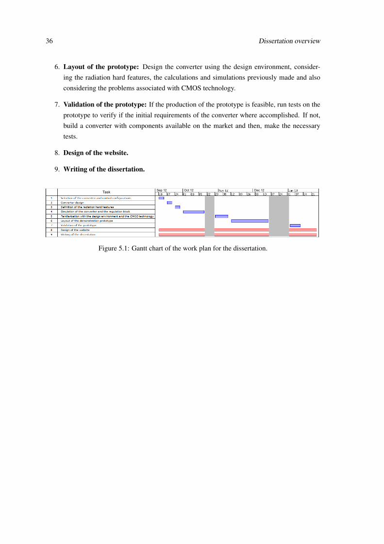
36 Dissertation overview
6. Layout of the prototype: Design the converter using the design environment, consider-
ing the radiation hard features, the calculations and simulations previously made and also
considering the problems associated with CMOS technology.
7. Validation of the prototype: If the production of the prototype is feasible, run tests on the
prototype to verify if the initial requirements of the converter where accomplished. If not,
build a converter with components available on the market and then, make the necessary
tests.
8. Design of the website.
9. Writing of the dissertation.
Task Sep 12 Oct 12 Dec 12
Figure 5.1: Gantt chart of the work plan for the dissertation.

References
[1] Robert W. Erickson and Dragan Maksimovic. Fundamentals of Power Electronics. KluwerAcademic Publishers, second edition, 2004.
[2] Robert Boylestad and Louis Nashelsky. Electronic devices and circuit theory. Prentice Hall,seventh edition, 1998.
[3] Adel S. Sedra and Kenneth C. Smith. Microelectronic Circuits. Oxford University Press,fifth edition, 2004.
[4] Ned Mohan, Tore M. Undeland, and William P. Robbins. Power Electronics. Convertes,Applications and Design. John Wiley and Sons, Inc, third edition, 2003.
[5] AN77. CMOS, the Ideal Logic Family. Application Note 77. Fairchild Semiconductor,January 1983.
[6] R. Jacob Baker, Harry W. Li, and David E. Boyce. CMOS. Circuit design layout and simu-lation. IEEE Press, 1998.
[7] K. Viswanathan, R. Oruganti, and D. Srinivasan. Dual-mode control of tri-state boost con-verter for improved performance. Power Electronics, IEEE Transactions on, 20(4):790 –797, july 2005.
[8] Rong-Jong Wai and Yi-Chang Chen. Automatic fuzzy control design for parallel dc-dc con-verters. Proceedings of the International MultiConference of Engineers and Computer Sci-entists (IMECS), I, March 2009.
[9] I. Barkana. Classical and simple adaptive control for nonminimum phase autopilot design.Journal of Guidance, Control And Dynamics, 28(4):631–638, 2005.
[10] Goo-Jong Jeong, In-Hyuk Kim, and Young-Ik Son. Application of simple adaptive controlto a dc/dc boost converter with load variation. In ICCAS-SICE, 2009, pages 1747 –1751,aug. 2009.
[11] P. Mattavelli, L. Rossetto, G. Spiazzi, and P. Tenti. General-purpose fuzzy controller fordc-dc converters. Power Electronics, IEEE Transactions on, 12(1):79 –86, jan 1997.
[12] Sumita Dhali, P. Nageshwara Rao, Praveen Mande, and K.Venkateswara Rao. Pwm-basedsliding mode controller for dc-dc boost converter. International Journal of EngineeringResearch and Applications (IJERA), 2(1):618–623, Jan-Fev 2012.
[13] István Nagy and Pavol Bauer. Dc-dc converters. In Power Electronics ans Motor Drives.CRC Press, 2011.
37
38 REFERENCES
[14] Liu Zhi, Yu Hong-bo, Liu You-bao, and Ning Hong-ying. Design of a radiation hardeneddc-dc boost converter. In Information Engineering and Computer Science (ICIECS), 20102nd International Conference on, pages 1 –4, dec. 2010.
[15] Jacob Millman and Arvin Grabel. Microelectronics. McGraw-Hill, second edition, 1988.
[16] R. P. Jain. Modern Digital Electronics. Tata McGraw-Hill, third edition, 2003.
[17] G. Kishor, D. Subbarayudu, and S.Sivanagaraju. A fuzzy logic based two inductor boostconverter system. International Journal of Engineering Science and Technology (IJEST),4(1):295–302, January 2012.
[18] Abraham Yoo. Design, Implementation, Modeling, and Optimization of Next GenerationLow-Voltage Power MOSFETs. PhD thesis, Department of Materials Science and Engineer-ing University of Toronto, 2010.
[19] P. Mattavelli, L. Rossetto, G. Spiazzi, and P. Tenti. General-purpose sliding-mode controllerfor dc/dc converter applications. IEEE Power Electronics Specialists Conf. Rec. (PESC),1993.
[20] Vadim Ivanovich Utkin, Jürgen Guldner, and Jingxin Shi. Sliding Mode Control in Elec-tromechanical Systems. Taylor and Francis, 1999.
[21] Anthony Jordan. Radhard-by-design integrated circuit suppliers: A success story. MilitaryEmbedded Systems, 2006.
[22] P.C. Adell. Total-dose and single-event effects in switching dc/dc power converters. IEEETransactions on Nuclear Science, 46(6):3217–3221, 2002.