radar signal processing - walter scott, jr. college of...
TRANSCRIPT
Radar Signal Processing: Hardware Accelerator and Hardware Update
Academic Year 2007-2008
by
Michael Neuberg
Christopher Picard
Prepared to partially fulfill the requirements for ECE401/ECE402
Department of Electrical and Computer Engineering
Colorado State University
Fort Collins, Colorado 80523
Report Approved:
Project Advisor
Senior Design Coordinator

ii
Abstract
This project consists of two different projects both dealing with Colorado State University’s (CSU’s) radar systems. The first project is to update CSU’s Pawnee Doppler radar system. This will be done to improve performance and ability to enhance data. The second project deals with adding a hardware accelerator to the implementation for the Parametric Time Domain Method (PTDM) clutter mitigation algorithm. The device used in the hardware acceleration will be graphics cards.
The antiquated Pawnee radar system is outdated, which makes it hard to find replacement parts and limits the performance. The main retrofit is to replace the sychros, which give rotational position, with optical encoders. This should improve the resolution ten times, which enhances the system’s range over long distances. For the PTDM clutter mitigation implementation a standard computer system cannot compute results in real time. Graphics cards can perform needed calculations at rapid rates. This will allow the algorithm to be applied in real time.
Updating the system by using optical encoders requires interfacing to the Digital Signal Processor (DSP). A Field Programmable Gate Array (FPGA) will be used to send data to and from the encoders, then to the DSP. This will act as the interface between the two devices. A printed circuit board will be made with the FPGA to transmit and receive the data. The hardware that will be used is a Xilinx Spartan-3E FPGA and Stegmann ARS-20 absolute optical encoder. This hardware will then be installed at the Pawnee radar system which will improve the data about the position of the radar antenna. When researching different graphics cards to use for the implementation of the PTDM, clutter mitigation algorithm the Nvidia Quadro FX 5600 was chosen. The graphics card has 16 multiprocessors each of which can execute 128 simultaneous threads. Nvidia has a language called Compute Unified Device Architecture (CUDA). This language allows the programmer to use a C style language to code tasks on the graphics cards. This will greatly speed up production time for the implementation.
iii
Acknowledgments
The authors of this paper would like to thank Dr. Chandra for the opportunity to work on this project. It has given us valuable experience with the radar facilities at Colorado State University (CSU). We would also like to thank Jim George as well as the rest of the graduate students that are part of the CSU radar research team. We could not have gotten this far on our project without their guidance.
We would like to thank the CSU CHILL facilities for donating the components to help research and test for the CSU Pawnee update project. We would also like to thank Hewlett Packard for their donation of the workstation platform and graphics cards to the hardware accelerator project.

iv
TABLE OF CONTENTS
Title i
Abstract ii
Acknowledgments iii
Table of Contents iv
List of Figures and Tables v
I. Introduction 1
II. Background Information of Radar & CSU Facilities 2
III. Hardware Accelerator 3
A. Review of Previous Work 3
B. Problem Requirements and Solution Approaches 6
C. Solution Implementation 7
C.1 Hardware 7
C.2 CUDA Implementation 8
C.3 Current Project Status 10
IV. Pawnee Hardware Update 12
A. Colorado State University Pawnee Radar Facility 12
B. Pawnee Hardware 13
C. Problems Arising With Old Hardware 13
D. Solution 15
E. Implementation of Software 16
F. Implementation of Hardware 18
F.1 Components and Requirements 18
F. 2 PCB Design and Layout 20
V. Future Work and Conclusions 27
References 29
Bibliography 30
Appendix A – Abbreviations 31
Appendix B – Budget 32
Appendix C – Gray to Binary Comparison 33

v
Appendix D – PCB Components List 34
Appendix E – Circuit Board Schematic Layout 35
List of Figures
Figure 1 CHILL Doppler Radar Facility 2
Figure 2 Pawnee Doppler Radar Facility 3
Figure 3 PPI without Ground Clutter Filter 4
Figure 4 PPI with Ground Clutter Filter 5
Figure 5 Nvdia CUDA Architecture 9
Figure 6 Benchmark Results 10
Figure 7 PPI CHILL Radar Image, 2003, Tornado 14
Figure 8 Pawnee Radar Inside the Radome 16
Figure 9 Clock Signal and Encoder Data 17
Figure 10 Xilinx XPower Estimator Tool 19
Figure 11 PCB Top Layer 22
Figure 12 PCB Ground Plane 23
Figure 13 PCB Power Plane 25
Figure 14 PCB Top Layer and Power Layer 26
List of Tables
Table 1 FX 5600 Specifications 7

1
I. Introduction
There are two separate projects that are integrated together to benefit both of Colorado
State University (CSU’s) radar sites. The first project is to address the issue of ground clutter on
a radar image. There are several methods for mitigating ground clutter, each method having its
own benefits and disadvantages. This report will discuss one of the more effective ground clutter
mitigation techniques, as well as the difficulties in implementing the approach.
This report will cover a method for creating a hardware accelerator in order to perform
matrix calculation in parallel to significantly reduce the computation time. It will use a unique
preset architecture on a graphics card. Using the architecture and a C based extension language,
the graphics card will be transformed into the hardware accelerator for this project. Using this
hardware accelerator will allow one of the ground clutter mitigation methods to be preformed in
real time.
The second project contains information to update hardware at one of the CSU radar
facilities. Most of the hardware is outdated, which makes it hard to find replacement parts.
Updating the hardware will enhance the radar positioning system and will provide more precise
data. The main hardware update will be to replace synchros with encoders to determine the
precise angle and direction where the dish is directed. More details of the project will be
discussed along with the methods of implementation.
First, a background description of how radar works and the history will be discussed.
Then information on the two CSU radar facilities will be provided. Chapter III will deal with the
hardware accelerator project details. Chapter IV will discuss the specifics of the hardware

2
update. The last section will discuss wrap up the two projects and give an idea of future work to
be completed.
II. Background Information on Radar and CSU Facilities
The basic idea of radar is very simple. During WWII when ships or airplanes would
cross the path of radio signals, their echoes would be heard. This led to the idea of using radio
signals to determine the location of objects. This technology was further developed during
WWII forward to current day innovations. Many great technological advances have been made
to benefit the development of radar today. Much research continues today to improve and
enhance radar systems.
Understanding how radar works is a very simple idea. Radar basically consists of four
parts: 1.) there is the transmitter that generates a signal, 2.) an antenna that sends and receives
the signal, 3.) a receiver that detects the signal, and 4.) a display unit to analyze the data. All
these components make up very complex radar systems.
Colorado State University currently uses two radar facilities. The CHILL Doppler radar
(Figure 1) is a dual polarized S-band system located by Greeley, Colorado.
Figure 1 CHILL Radar Facility

3
The other is the Pawnee Doppler radar (Figure 2) which is a single polarized S-band system
located by Nun, Colorado..
Figure 2 Pawnee Radar Facility
Both radar facilities are combined to operate as a dual-Doppler configuration. The waveform
generated is a Gaussian waveform. Then a Klystron amplifier charges up the waveform to
1MW/channel. Next this is sent to the transmitter and sent off into the sky. Both of these
systems are sponsored by the National Science Foundation and Colorado State University.
III. Hardware Accelerator
A. Review of previous work:
One of the major problems that weather radar systems face is ground clutter. Ground
clutter is when the radar beam bounces off objects located on the ground. These objects can be
trees, buildings, mountains, et cetera. In order get a good weather image over areas with ground
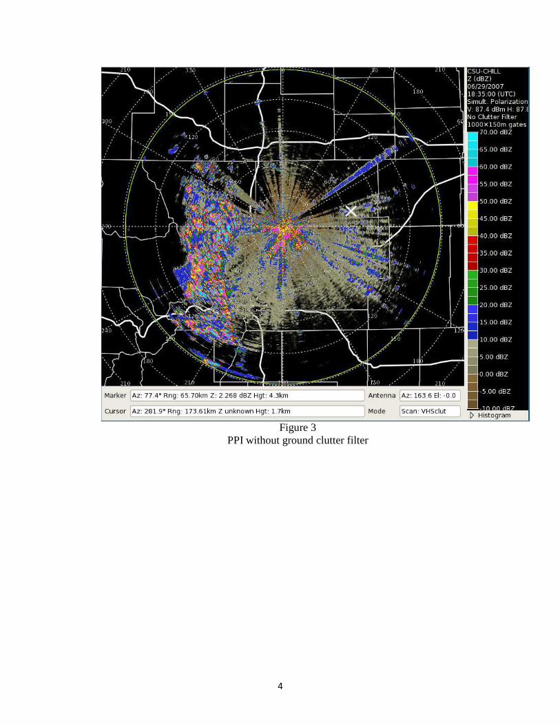
clutter a clutter mitigation algorithm must be applied. In Figure 1 there is a Plan Position
Indicator (PPI) image with no ground clutter mitigation approaches applied. Figure 2 shows an
image seconds later with a ground clutter mitigation approach applied.
4
Figure 3 PPI without ground clutter filter

5
Figure 4 PPI with Ground Clutter Filter
As one can see, this filter significantly reduces the presence of ground clutter. It does not
reduce the clutter completely.
Parametric Time Domain Method (PTDM) is a method for radar ground clutter
mitigation. This method helps suppress the effect of ground clutter close to the radar site. Unlike
previous methods, this approach does not have the problem of signal loss or spectral leakage
(Nguyen, Moisseev, Chandaraskar 2007). The reason PTDM is not subject to these problems is
because it does not apply Fourier transforms on the signal switching the domain. Instead the
method performs its calculations in the time domain. The main issue with the PTDM approach is

6
it requires computationally expensive calculations. This is primarily due to the complex matrix
calculations that must be performed on large matrixes. When simulated in Matlab, the
calculations were shown to be too slow to run on a standard personal computer.
B. Problem Requirements and Solution Approach:
The problem is to find an approach to implement a hardware accelerator for calculating
matrix operations which includes determinates and inverse. The accelerator must be able to
perform the calculation at a rate to implement the PTDM algorithm in real time.
The chosen implementation was to perform the matrix calculations on a Graphics
Processing Unit (GPU). A GPU is a processor that is located on a graphics card. In order for a
graphics card to render images and handle the movement of those images on a screen, it must
perform large numbers of floating point operations in a small amount of time. The GPU
accomplishes this by performing large number of these operations in parallel, as well as
optimizing floating point operations. Both of these factors make the GPU an ideal choice for
implementing PTDM.
C. Solution Implementation:
This section will talk about the hardware the PTDM will be implemented on. It also
discusses the method for turning a GPU into a useable hardware accelerator.
C.1 Hardware:
There were two graphics cards venders researched as possible suppliers for this project.
The first vender is ATI graphics cards. ATI has a development method called Close To the Metal
(CTM). This development tool allows the user to write a custom driver level piece of code for
7
the graphics card. The primary disadvantage of this approach is the learning curve for
development.
The second vender is Nvidia. Nvidia has a development method called Compute Unified
Design Architecture (CUDA). This method builds a general architecture on the graphics card and
then allows the user to write in a C style language making special function calls to compute on
the graphics card. With this C style language development time is significantly shorter.
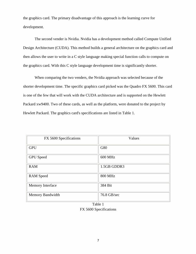
When comparing the two venders, the Nvidia approach was selected because of the
shorter development time. The specific graphics card picked was the Quadro FX 5600. This card
is one of the few that will work with the CUDA architecture and is supported on the Hewlett
Packard xw9400. Two of these cards, as well as the platform, were donated to the project by
Hewlett Packard. The graphics card's specifications are listed in Table 1.
FX 5600 Specifications Values
GPU G80
GPU Speed 600 MHz
RAM 1.5GB GDDR3
RAM Speed 800 MHz
Memory Interface 384 Bit
Memory Bandwidth 76.8 GB/sec
Table 1 FX 5600 Specifications
8
The xw9400 was chosen since it has two full 16-bit channel PCIe slots. This allows for
data to be transferred from main memory to the graphics card memory at a higher rate. The
system has two AMD Opteron processors. This provides a high-end processor to accurately
access the speed of the CUDA implementation.
C .2 CUDA Implementation:
In order to turn the two graphics cards into hardware accelerators CUDA will be used.
This architecture turns the graphics card into multiprocessor blocks. Each of these
multiprocessors has eight individual processors with dedicated registers as well as access to
shared memory. There are 8,192 registers and 16 KB of shared memory per multiprocessor
block. (Nvidia CUDA Programming Guide 2007). For the entire architecture see Figure 5.

9
Figure 5 Nvidia CUDA Architecture
The software implementation of CUDA is a C style language. When an operation is to be
performed on the graphics card, a segment of code called a kernel is executed. Each kernel is
broken up into an array of blocks. Each block consists of a large number of threads. Only one
block can be executed on a multiprocessor at a time; however, other blocks can be swapped on to
the multiprocessor in order to optimize performance when a block is in an idle section.

10
In order to use this architecture in a high performance setting, there are some important
constraints to understand. The most important constraint is having 16 KB of shared memory. All
of the data you are processing per multiprocessor must be able to fit in the 16 KB shared memory
space. If all of the data cannot fit in the shared memory, then there is a 400 to 600 clock cycle
delay per read from any data not in shared memory (Nvidia CUDA Programming Guide 2007).
The second constraint is all threads are organized into a group of 32 called a warp. This means
that to get optimal performance there must be a minimum of 64 threads per block. The last
important constraint is the memory layout of the device. Shared memory blocks are organized
into sixteen, one byte blocks. No thread can access the same memory block at the same time.
Global memory is organized in a different manner, however, in order to get optimal read times
each thread should read form it at 32 bit intervals (Nvidia CUDA Programming Guide 2007).
C .3 Current Project Status:
The first important segment of code for implementing PTDM is the inverse operator. It is
the operator that involves the most floating point computations out of PTDM. The current
performance of the inverse operator is shown in Figure 6. The x axis represents the number of 16
x 16 matrices the inverse was performed on.

11
Figure 6 Benchmark Results
The performance of CUDA shown is greatly improved from the original implementation
that had a speed at 10000 matrices of 7.9 sec. CUDA still has a 33% slower performance then the
systems processor. This performance difference has been shown to be due to the data transfer
rates from memory to the graphics card. When the inverse operator is preformed on the data ten
times, the CUDA implementation’s performance becomes 35% faster than the system processor.
There are three key improvements made from the original implementation of the CUDA
code. The first improvement was implementing a batch type data transfer structure from main
memory to the graphics card memory. Instead of sending all of the data at the same time to the
graphics card, batches of 100 matrices are sent instead. This single improvement increased the
performance from 7.9 sec. to 1.2 sec on 10000 matrices. The second improvement was to the use
of host page locked memory. This method makes the pages that contain the data that is to be
16x16 Results
0
0.1
0.2
0.3
0.4
0.5
0.6
0.7
0.8
500 1000 2000 3000 4000 5000 6000 7000 8000 9000 10000
Gates
Sec
Single
Double
CUDA

12
transferred onto the graphics cards to be locked in their location in memory. The system will no
longer be able to move the data to a different memory location or page the data out of main
memory. The end result of this restriction is a data transfer rate between main memory and the
graphics card at twice the original rate. The last improvement was to calculate the inverse of two
matrices per block. Due to data dependency of the inverse operation, it is difficult to fully utilize
the parallelism of the graphics card. By adding the second matrix, it allows for double
performance in low parallel sections of the inverse operator. No more matrices could be added
due to the 16 KB limitation on shared memory.
The next important operator that PTDM involves is calculating a matrix determinate. The
code for this operator is not complete at present time, but is slated to be finished within the next
two weeks. With the data transfer structure, the inverse and the determinate operator the
remaining parts of PTDM will take less time then these three parts.
IV. Pawnee Hardware Update
The goal of this project is to update the positioning system and hardware on the CSU-
Pawnee Doppler radar. This will be done by replacing synchros with optical encoders and
interfacing them to the radar signal processor using an FPGA. This will greatly improve the
accuracy of this site.
A. Colorado State University Pawnee Radar Facility
The Pawnee radar is located about 48km north of the CSU-CHILL radar in Greeley.
This radar was shown before in Figure 2. The antenna is located within the radome on the right-
hand-side. The trailer on the left is where all the main radar hardware, electrical equipment, and
operators are located. This is a single-polarization radar system, which means it only transmits
signals on one axis.

13
B. Current Pawnee Hardware
The old Pawnee radar has outdated equipment. This old equipment makes it hard to fix
and find replacement parts. While this radar still works fine, it can definitely be enhanced.
Right now the radar uses synchros, which were developed during WW II, to communicate
rotational position to the operator. The two types of rotational position are the azimuth position
and the elevation position. Synchros use many wires to transmit the data in parallel over long
distances, which in turn can be very costly, prone to noise, and prone to damage. Due to all the
wires and the age of the synchros, only so many bits of resolution can be determined. The
current synchros have a resolution of approximately 0.1 with the number of data bits available.
C. Problem Arising With Old Hardware
What sort of error can be caused from the low resolution of the synchros? An example of
a typical radar image is shown below in Figure 7.

14
Figure 7 PPI CHILL Radar Image, 2003, Tornado
This was taken in August 2003 from the CHILL facility of Burns, Wyoming, which is
approximately 100km away. The area within the big circle represents a tornado given by the
“hook” shape that the reflectivity is making. If the image above was from the Pawnee radar site,
and not from CHILL, the following errors can be calculated due to the low resolution of the
synchros.
From the radar at the center suppose that the tornado was located at an angle of 75o.
15
x=25.8819km
y=96.5926km
The simple law of sines can show the precise location of the tornado. If the degree is off
by 0.1, then the resulting error can occur.
x=26.0505km
y=96.5473km
This can place the tornado almost 0.2km (656ft) from where it actually is. If this value
could be improved to track the exact location of the weather system, people who were directly in
the path of the tornado could be warned. This is only for 100km away. However, many weather
radars can go up to a few hundred kilometers away, which increases the error caused by the low
resolution. The goal is to improve these values.
D. Solution
A good solution to the issue of low resolution is to use optical encoders. Absolute
encoders from Stegmann, ARS-20, were purchased to replace the synchros. Absolute encoders
are used because the position data is still retained even after power loss. This is important
because the radar is not operational all the time. The absolute encoder was compared to an
incremental encoder that loses its position upon power loss. An absolute encoder was by far the
best choice. The best thing about this encoder is that it transmits 15 bits of data serially for each
position. This means that there are 2 to 32,768 different values that this can read within 360o.
This gives a resolution of 0.01. By doing the same math as before with the better resolution, the
error for 100km is only off by 0.02km (65ft), which is very good. Another benefit to using
optical encoders is the fact that they are not susceptible to noise and electromagnetic
interference. They are also beneficial because it requires fewer wires to transmit data. Only two
wires are required to transmit data and two wires are used for a clock signal. This reduces noise
and cost with the wires. The encoder is shown below in Figure 8 with a view of the radar inside

16
the radome. It will go inside the platform where the synchros currently reside. One encoder is
needed to track the azimuth rotational position and one is needed for the elevation position.
Figure 8 Pawnee Radar Inside the Radome
E. Implementation of Software
To complete this project a Field Programmable Gate Array (FPGA) is used to act as the
interface between the optical encoders and the DSP unit. To test this project a Basys Digilent
development board was used, which contains a Xilinx Spartan-3E FPGA. This was used to
implement test code to check the data from the encoders. In the summer of 2007, a research
experience for undergraduate project was done by Darryl Benally and some of the code from that
was used as a reference. Many VHDL tutorials were used to develop the coding of this system.

17
The FPGA does the following processes to work correctly. First, to properly receive data
from the encoders the FPGA needs to generate a 17 pulse square wave. The encoder transmits
15 bits of data and 2 error bits. The radar transmits waves approximately once every
millisecond. In order to get one data bit from the encoders with each transmission, the minimum
clock signal needs to be 1kHz per bit. With 17 bits per encoder the clock signal needs to be at
least 17kHz if a reading is required every time the radar sends a signal. A faster clock signal
would allow for more readings during the transmit time. This project is done using a 1MHz
clock signal in order to get many data readings for each radar transmission. With a clock signal
going to each encoder, one elevation and one azimuth, the encoder will be sending back the data
of 17 bits on two separate lines. The FPGA needs to read in this data and process it.
The encoder transmits the data in Synchronous Serial Interface (SSI) format which is
patented by Stegmann. The signal is held high then a low signal initiates the sequence. Data is
sent back on each rising edge. An important part is to put a delay between successive clock
signals so the data sets can be distinguished. An example of the clock signal needed to be sent to
the encoder would be to start high then transmit a square wave with 17 steps then finish high.
An example of the clock and data signal is shown in Figure 9. The encoder data on the bottom
represents a 15 bit serial data stream.
Figure 9 Clock Signal and Encoder Data

18
After this, then wait and repeat the signal. The benefits of SSI is the need for only 4 data lines,
low conventional component count, and one can store data simultaneously.
Once the data is received by the FPGA from the encoder, it is processed. First, it must be
converted from Gray code to binary. Then one of the data sets needs to be shifted so that the
elevation and azimuth position data can be combined into the same thirty-two bit word of data.
This is called the “parallel to serial conversions” because the data from two parallel lines is able
to be transmitted on one single serial line. The single set of data is then transmitted over fiber
optic lines to the radar signal processor unit. The whole process is completed in less than a
millisecond, meaning the data coming from the radar position will always be accurate.
F. Implementation of Hardware
To complete this project a Printed Circuit Board (PCB) is needed to hold all the
components. The board is designed using PCB Artist from Advanced Circuits. In order to
accomplish this, much review of the current board layouts and components was needed. Another
important consideration was to find components that were available on Digikey in the useable
packages.
F.1 Components and Requirements
A schematic on the Basys board from Digilent was used as a reference for general
configurations. An important difference in the project design versus the test board is the FPGA.
The software used to program the device, the available FPGA devices, and the PCB parts all
needed to match up. A Xilinx Spartan 3 FPGA was used, which is a different pin out and
specifications from the development board’s Spartan 3E chip. The device has less gates and less
19
functionality, but for this project is very adequate. Powering on the FPGA is actually a very
difficult task with it requiring 3 different voltage levels. A nice feature with using Xilinx chips is
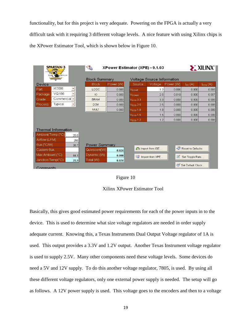
the XPower Estimator Tool, which is shown below in Figure 10.
Figure 10
Xilinx XPower Estimator Tool
Basically, this gives good estimated power requirements for each of the power inputs in to the
device. This is used to determine what size voltage regulators are needed in order supply
adequate current. Knowing this, a Texas Instruments Dual Output Voltage regulator of 1A is
used. This output provides a 3.3V and 1.2V output. Another Texas Instrument voltage regulator
is used to supply 2.5V. Many other components need these voltage levels. Some devices do
need a 5V and 12V supply. To do this another voltage regulator, 7805, is used. By using all
these different voltage regulators, only one external power supply is needed. The setup will go
as follows. A 12V power supply is used. This voltage goes to the encoders and then to a voltage
20
regulator to take it down to 5V. This 5V is used by some devices, but then it is also divided
down to 1.2V, 2.5V, and 3.3V for other devices.
Other components include a crystal oscillator running at 40MHz. This is used to by the
FPGA to send a clock signal to the encoders. A Xilinx Programming Platform Flash chip is also
used to program the device. This ties the JTAG programming cable to the FPGA and allows the
device to be programmed. Differential line drivers and receivers are used in order to transmit
and receive data from the encoders. These are used to distinguish between the high and low TTL
signals over long distances. A dual peripheral driver is also used for TTL outputs. These signals
are then sent to a fiber optic transceiver, which sends the signal to the DSP unit and angle
display. A detailed parts list can be found in Appendix D. As said before all these parts are
easily available through electronic component providers.
F.2 PCB Design and Layout
A schematic design was the first step is the PCB process. Using PCB Artist, a schematic
layout was created. This involved connecting nets, choosing parts, and creating parts. The
correct package size and specifications of each component were taken into consideration. This
was basically broken down into six different sections: power, transmitter, receiver, flash
memory, clock, and programming. These sections can be seen in Appendix E.
Once the schematic was completed, then this was translated in a printed circuit board
layout. Each component was then placed in a logical position in relation to the routing
requirements of the board. Everything was then routed with copper traces.
At first the design started as a two layer PCB board. This proved to be very difficult and
hard to follow traces. The overall flow of the nets in this design was very poor. Many
components were hard to place and then hard to route to where needed. Due to the difficulties
with a two layer board, a decision was made to use a four layer board. This allowed a top layer,
21
ground layer, power layer, and bottom layer. By using this type of board, the flow improved and
it was much easier to route all the components.
The top layer contained approximately 95% of the components, which is easier to follow
the flow. Many decoupling capacitors are used on the inputs and outputs to most pins to reduce
noise. These needed to be placed very close to the pin. All the parts are labeled and documented
on the top silk screen of this top layer. Due to the benefits of a four layer board, extra
components are able to be added to this top layer. This included extra dip component options
and other small parts so this board can be added onto later if needed. The top layer can be
viewed in Figure 11 below. The bottom layer, not shown, was basically only used for a few
decoupling capacitors and copper traces.

22
Figure 11
PCB Top Layer
The ground plane was one of the biggest advantages to using a four layer board. This
allowed for a ground connection from almost any point on the board, while with a two layer
board many nets where used to connect ground at various points. The ground plane is shown
below in Figure 12.

23
Figure 12
PCB Ground Layer
The black represents the copper pour area and white is the etchings. Whenever a component
needed to be grounded then a via was added to connect straight to the ground plane. The white
star pattern shows vias that are connected to this plane. The star pattern is used for thermal relief
in that heat will not concentrate to one location on the plan, but can be dispersed through four
sides. Some components, such as heat sinks on the top copper layer, require many vias with

24
thermals to dissipate heat. The rings are components that do not touch the ground plane and go
through to another layer.
Another concern about the Pawnee Radar site is that it frequently gets struck by
lightning. This could potentially destroy the board through the connections. In order to prevent
this, modifications to the ground plane were made. An outer ground ring partially isolated from
the inner ground layer was created to prevent destruction of the components. Any permanent
connectors, such as the encoders, have the wire shielding connected to this outer ring. That way
if charge builds up in the wire, it will travel around the outside edge and up to the upper right
side of the board where the power supply will be. This way the charge does not travel across the
middle of the board where the FPGA and all the components are located. It still makes a
common ground for all by being connected in the upper right hand corner.
A power plane layer was also used in order to provide all the components with the
needed supply. This involved carefully planned out polygon pours according to the component
locations. The power layer is shown below in Figure 13.

25
Figure 13
PCB Power Layer
As one can see, each isolated area represents a different voltage level. The voltage dividers are
placed between the two planes so that it can take in the input voltage from one area, and then
output the voltage to another area. As with the ground plane, this plane is connected to through
vias with thermals to disperse the flow of the current and heat. This design allows for voltage
levels of 12V, 5V, 3.3V, 2.5V, and 1.2V all from only one power source. This is important
because of all the different voltage requirements for the components and also the three separate
voltage levels needed by the FPGA. The board’s outline with component and power layer is

26
shown below in Figure 14 to show how all the voltage regulators supply power and where all the
components lie.
Figure 14
PCB Top Layer and Power Layer

27
V. Future Work and Conclusions
As of May 3, 2008 the Pawnee Hardware update project is almost complete. The board is
currently being manufactured and the parts have been ordered. They are expected to arrive
within the next few days. The next task will be to place and solder all the components to the
board. Once the board has been tested and checked, then the software program from fall
semester will be tested with the board. It will be tested against an angle display at the radar
facility to determine if it working correctly.
It is not recommend to continue this project in the future. The project will basically be
done within a week. The only task left to do would be actually installing the encoders at the
Pawnee site. This can easily be done sometime this summer when other maintenance work is
being completed at the Pawnee radar site.
It is difficult to say whether the hardware accelerator project should be continued.
Despite the clams that CUDA is an easy implementation method, there is an extremely high
learning curve and very little material available on it. This is what led to the full PTDM
algorithm not being implemented at present time. If this project is continued, a larger team is
required to help offset the difficulty of the implementation.
There are three main steps left in the hardware accelerator project. The first is to take the
existing code and add the rest of PTDM to it. After that step is accomplished the performance of
the code needs to be measured and improved until it is sufficient to implement PTDM in real
time. The final step will be to integrate the PTDM code with the present data interface at the
radar site. Once these steps are accomplished the project will be ready to be installed at the Chill
radar site.

28
After the implementation of the new encoders, hardware components, and software
components of the Pawnee retrofit project, CSU’s radar sites will have more accurate radar data
to be retrieved. Even though the PTDM implementation was not completed this semester, there is
now good base for future developers to build on. This will help to lower the large learning curve
associated with CUDA.
Given the facts outlined in the paper, these two projects will increase the accuracy of the
radar data in two different ways. The first will provide higher precision data and the second a
cleaner image. With the more accurate data, further research projects on the sites will benefit
from this project.

29
References:
[1] Absolute Encoder; Sick/Stegmann
[2] ARS 20, ARS 25: Single-turn Absolute Encoder; Sick/Stegmann
[3] CUDA Programming Guide 1.1, Nvidia; November 2007
[4] Digilent Basys Board Reference Manual; Digilent
[5] Digilent Basys Board Schematic Revision E; Digilent
[6] PCB Artist Layout Software Step by Step; Advanced Circuits
[7] PCB Artist Layout Software Part Creation; Advanced Circuits
[8] Spartan-3 generation FPGA User Guide; Xilinx; April 2007
[9] Spartan-3E FPGA Family: Complete Data Sheet; Xilinx; May 2007
[10] Synchronous Serial Interface for Absolute Encoders; Stegmann
30
Bibliography
[1] Benally, Darryl, 2007: Antenna Control for the Pawnee Radar. Colorado State University
[2] Nguyen, Cuong M., Dmitri N. Moisseev, and V. Chandrasekar, 2007: A parametric time domain method for spectral moment estimation and clutter mitigation for weather radars. Colorado State University
[3] Rinehart, Ronald E., 1997: Radar for Meteorologists. 3rd Edition: Knight Printing 2001

31
Appendix A- Abbreviations
CTM- Close To the Metal
CSU- Colorado State University
CUDA- Compute Unified Device Architecture
DCM- Digital Clock Manager
DSP- Digital Signal Processor
FPGA- Field Programmable Gate Array
PCB- Printed Circuit Board
PCIe- Peripheral Component Interconnect Express
PPI- Plan Position Indicator
PTDM- Parametric Time Domain Method
SSI- Serial Synchronous Interface
VHDL- VHSIC Hardware Description Language
VHSIC- Very High Speed Integrated Circuits

32
Appendix B- Budget
Item Price
Digilent BASYS Board $50
2 Quadro FX 5600 $3000 ($1,500 a piece)
2 Stegmann Absolute Encoder $1200 ($600 a piece)
xw 9400 $1500

33
Appendix C- Gray to Binary Comparison
Gray Code Binary Code Number
0000 0000 0
0001 0001 1
0011 0010 2
0010 0011 3
0110 0100 4
0111 0101 5
0101 0110 6
0100 0111 7
1100 1000 8

34
Appendix D- PCB Components List
1A Voltage Regulator 5V, Fairchild Semiconductor
40MHz Crystal Oscillator, CTS-Frequency Controls
5mm Terminal Block, On Shore Technology
600W Transient Voltage Suppressor, Diodes Inc
Dual Output Voltage Regulator 1.2V, 3.3V, Texas Instruments
Dual Peripheral Driver, Texas Instruments
ESD Diode Array, NXP Semiconductors
Fiber Optic Transceiver, Agilent
Heatsink, Aavid Thermalloy
Linear Voltage Regulator 2.5V, Texas Instruments
Platform Flash, Xilinx
Quadruple Differential Line Receiver, Texas Instruments
Quadruple Differential Line Driver, Texas Instruments
Spartan -3 FPGA, Xilinx
Various Size Resistors
Various Size Capacitors

35
Appendix E- Circuit Board Schematic Layout
Power Schematic

36
Transmitter Schematic

37
Receiver Schematic

38
Flash Memory Schematic

39

40
Clock Schematic
Programming Schematic

41