quixote 2070l operating manual - peektraffic.com operating... · electronic industries association...
TRANSCRIPT

Operating ManualOperating Manual
2070LAdvanced Traffic Controller


Operating Manual
MMMooodddeeelll 222000777000LLL 222000777000 AAAdddvvvaaannnccceeeddd TTTrrraaaffffffiiiccc CCCooonnntttrrrooolllllleeerrr
Unit/Module Part Number Revision
2070L 2070-L-04 1
2070-1B 106271 106335
E1 F
2070-2A 104697 104467
D2 A
2070-3B 106104.2 C
2070-4A 2070-4B
106499 G
Part Number: 99-446, Rev 1 Last Edited: September 28, 2006
Equipment Described: Unit s/n 3018210906 or higher, Rev 1. Manufactured on or after August of 2006

Copyright
Copyright © 2006 Quixote Traffic Corp. All rights reserved.
Information furnished by Quixote Traffic is believed to be accurate and reliable, however Quixote does not warranty the accuracy, completeness, or fitness for use of any of the information furnished. No license is granted by implication or otherwise under any intellectual property. Quixote reserves the right to alter any of the Company's products or published technical data relating thereto at any time without notice.
No part of this publication may be reproduced, stored in a retrieval system, or transmitted in any form or via any electronic or mechanical means for any purpose other than the purchaser’s personal use without the expressed, written permission of Quixote Traffic Corp.
Quixote Traffic Corporation 9603 John Street Santa Fe Springs, CA 90670 U.S.A.
Trademarks
US Traffic Corporation, Peek Traffic Corporation, Quixote Traffic Corporation and their associated logos are trademarks or registered trademarks of Quixote Corporation in the USA and other countries. Other brands and their products are trademarks or registered trademarks of their respective holders and should be noted as such.

Model 2070L Operating Manual • iii
Table of Contents Quick Contents These are the major sections and their locations within the 2070L manual:
Table of Contents............................................................................ iii 1 Glossary..................................................................................... 1 2 General Description ................................................................... 5 3 General Characteristics ........................................................... 15 4 Installation................................................................................ 19 5 Adjustments ............................................................................. 27 6 Theory of Operation................................................................. 31 7 Maintenance ............................................................................ 71 Index ............................................................................................. 73
Complete Table of Contents This manual contains the following sections:
Table of Contents............................................................................ iii 1 Glossary..................................................................................... 1 2 General Description ................................................................... 5
2.1 Chassis ............................................................................ 6 2.2 Lite CPU Module.............................................................. 7 2.3 Field I/O Module............................................................... 8 2.4 Display Module ................................................................ 9 2.5 Power Supply Module...................................................... 9 2.6 Asynchronous Serial Module ......................................... 12 2.7 Additional Optional Modules .......................................... 13
2.7.1 FSK Modem Module............................................... 13 2.7.2 Ethernet Module ..................................................... 13 2.7.3 GPS/Comms Module.............................................. 14 2.7.4 Synchronous Serial Module ................................... 14
3 General Characteristics ........................................................... 15 3.1 Standards Compliance .................................................. 15 3.2 Environment................................................................... 15 3.3 Power Specifications ..................................................... 15
3.3.1 Power Specifications — Power Supply Module ..... 15 3.3.2 Power Specifications — Plug-in Modules .............. 17
3.4 Electrostatic Discharge (ESD) Information .................... 17 4 Installation................................................................................ 19
4.1 Overview........................................................................ 19 4.1.1 Inspection of Hardware .......................................... 19 4.1.2 Handling ................................................................. 19

Contents
iv • Model 2070L Operating Manual
4.1.3 Environmental ........................................................ 19 4.2 Installing the 2070L in a Cabinet ................................... 19
4.2.1 Physical Installation................................................ 19 4.2.2 Grounding the Unit ................................................. 20 4.2.3 Connecting the Cabinet Harness to the Controller. 20 4.2.4 Wire Routing........................................................... 21
4.3 Installing the CPU Module in the Chassis...................... 22 4.4 Installing the Field I/O Module ....................................... 22 4.5 Installing the Display...................................................... 23 4.6 Installing the Power Supply Module in the Chassis ....... 24 4.7 Installing the Async Comm Module ............................... 25
5 Adjustments ............................................................................. 27 5.1 Overview........................................................................ 27 5.2 Chassis Adjustments ..................................................... 27
5.2.1 Mechanical Adjustments ........................................ 27 5.2.2 Electrical Adjustments ............................................ 27
5.3 CPU Adjustments........................................................... 27 5.4 Field I/O Adjustments..................................................... 27
5.4.1 SP3 ON Adjustment ............................................... 27 5.4.2 Muzzle Jumper Adjustment .................................... 28
5.5 Display Adjustments ...................................................... 28 5.6 Power Supply Adjustments............................................ 28 5.7 Async Comm Module Adjustments................................ 29
6 Theory of Operation................................................................. 31 6.1 System Overview........................................................... 31 6.2 Detailed Systems Description........................................ 32
6.2.1 Chassis................................................................... 32 6.2.2 Serial Port Operation.............................................. 35 6.2.3 CPU Module ........................................................... 37 6.2.4 Field I/O Module ..................................................... 42 6.2.5 Display Module....................................................... 58 6.2.6 Power Supply Module ............................................ 66 6.2.7 Async Serial Module............................................... 69
7 Maintenance ............................................................................ 71 7.1 Preventive Maintenance ................................................ 71 7.2 Trouble Analysis ............................................................ 71
7.2.1 Field Diagnosis....................................................... 71 7.2.2 Laboratory Diagnosis ............................................. 71 7.2.3 Hardware Failure Diagnosis ................................... 71
7.3 Troubleshooting Sequence Chart .................................. 71 7.3.1 Preliminary Checks ................................................ 71 7.3.2 Power Supply Checks ............................................ 72 7.3.3 Further Troubleshooting ......................................... 72

Contents
Model 2070L Operating Manual • v
7.4 Wave Forms................................................................... 72 7.5 Voltage Requirements ................................................... 72 7.6 Alignment Procedures ................................................... 72
Index ............................................................................................. 73

Contents
vi • Model 2070L Operating Manual
Table of Figures
Figure 1 – Complete 2070L Unit (front view) ................................ 5 Figure 2 – 2070 Chassis (front view) ............................................. 6 Figure 3 – 2070 Chassis (rear view) .............................................. 6 Figure 4 – 2070-1B Lite CPU Module (card front) ......................... 7 Figure 5 – 2070-1B Lite CPU installed in chassis (back of unit) .... 7 Figure 6 – 2070-2A Field I/O Module (card front) .......................... 8 Figure 7 – 2070-3B Display Module............................................... 9 Figure 8 – 2070-4 Power Supply Module (unit front view)............. 9 Figure 9 – 2070-4 Power Supply (unit rear view)......................... 10 Figure 10 – 2070-4B installed in the rear of the 2070 chassis..... 11 Figure 11 – 2070-7A Async Serial module .................................. 12 Figure 12 – 2070-6A Async/Modem Comm Module .................... 13 Figure 13 – 2070-6E Ethernet module......................................... 13 Figure 14 – 2070-6G GPS/Comms module ................................. 14 Figure 15 – 2070-7B Sync Serial module .................................... 14 Figure 16 – Location of Muzzle jumper & SP3 ON ...................... 28 Figure 17 – Block diagram of the basic 2070L modules.............. 31 Figure 18 – Chassis block diagram.............................................. 32 Figure 19 – CPU Host board block diagram ................................ 37 Figure 20 – CPU Engine Board block diagram............................ 41 Figure 21 – Field I/O Module block diagram................................ 42 Figure 22 – Display Module block diagram.................................. 59 Figure 23 – Power Supply block diagram .................................... 66 Figure 24 – Async Serial Module block diagram.......................... 69

Model 2070L Operating Manual • 1
1 Glossary These are terms that are useful when using this manual:
Ω .......................... ohm, a unit of electrical resistance µA ........................ microampere µs......................... microsecond 4U ........................ Height of 4 EIA standard units, size of chassis and
modules A .......................... Ampere AC........................ Alternating Current AC+...................... a 120 Volt AC, 60 Hertz ungrounded power source AC-....................... a 120 Volt AC, 60 Hertz grounded return to the
power source ACFAIL ................ AC failure ADDR................... address ANSI .................... American National Standards Institute Assembly ............. A complete machine, structure or unit of a machine
that was manufactured by fitting together parts and/or modules
Async. .................. asynchronous ATC...................... Advanced Traffic Controller Baud .................... Information Transfer Rate, usually bits per second BERR................... bus error Bus....................... Device that connects modules, usually a
motherboard Cabinet ................ An outdoor enclosure generally housing the
controller unit and associated equipment CD........................ Carrier Detect CPU ..................... Central Processing Unit CTS...................... Clear To Send Datakey................ a device for carrying portable data DC........................ Direct Current DRAM .................. Dynamic RAM EIA....................... Electronic Industries Association

Section 1 — Glossary
2 • Model 2070L Operating Manual
EIA-232 ................ EIA Bipolar Data Transmission Standard. EIA-232 uses a single wire for each signal. A positive voltage is used for one binary state while a negative voltage is used for the other. (Logic 1 = the negative level = “Mark”, Logic 0 = the positive level = “Space”) EIA-232 also defines the connector pin numbers and differs from EIA-574 in the type of connector used and pin out.
EIA-485 ................ EIA Balanced Differential Data Transmission Standard. EIA-485 uses a pair of wires, typically a twisted pair, to transmit Data and Inverted Data. EIA-485 allows multiple devices to be connected in parallel (multi-drop) on one data cable over distances of several miles. (Formerly known as RS-485, or RS485.)
EPROM................ Electrically Programmable ROM FCU...................... Field Controller Unit FLASH.................. A +5 VDC powered IC Memory Device with
nonvolatile, electrically erasable, programmable, IOOK read/write minimum cycles and fast access time features
FP......................... Front Panel GND ..................... Ground Hz......................... Hertz, Pure Unit Of Frequency In Cycles Per
Second I/O ........................ Input/Output IEEE..................... Institute of Electrical & Electronic Engineers IRQ....................... Interrupt Request IACK.................... Interrupt Acknowledge LCD...................... Liquid Crystal Display LED ...................... Light Emitting Diode LINESYNC ........... 60 Hz square wave synchronized to zero crossings
of power line lsb......................... least significant bit LSB ...................... Least Significant Byte mA........................ milliampere MC68302.............. Motorola IMP (Integrated Multiprotocol Processor) MC68360.............. Motorola QUICC (Quad Integrated Communication
Controller) Processor MIL-STD............... Military Standard Model 2070 .......... Controller Unit

Section 1 — Glossary
Model 2070L Operating Manual • 3
Model 2070-1....... CPU Module series Model 2070-2....... Field I/O Module series Model 2070-3....... Front Panel Assembly (FPA) series (aka ‘Displays’) Model 2070-4....... Power Supply Module series (either 2070-4A or
2070-4B) Model 2070-7....... Asynchronous Serial Communications Module
(ASCM) series Module ................. A functional unit part of an assembly MOV..................... Metal Oxide Varistor (form of surge protection
device) Motherboard ........ A printed circuit connector interface board msb ...................... most significant bit MSB..................... Most Significant Byte PCB ..................... Printed Circuit Board RAM..................... Random Access Memory ROM .................... Read-Only Memory RTS...................... Request To Send RX........................ Receive RXC ..................... Receive Clock RXD ..................... Receive Data SDLC ................... Synchronous Data Link Control SRAM .................. Static RAM STBY ................... Standby SYNC................... Synchronous SYSCLK............... System Clock SYSFAIL .............. System Fail SYSRESET.......... System Reset TIA ....................... Telecommunications Industry Association TEES ................... Transportation Electrical Equipment Specifications TTL ...................... Transistor-Transistor Logic TX ........................ Transmit TXC...................... Transmit Clock TXCI..................... Transmit Clock Input TXCO................... Transmit Clock Output TXD...................... Transmit DataUL ........................ Underwriter’s Laboratories, Inc. VAC ..................... Volts, Alternating Current line voltage VCC ..................... DC supply voltage VDC ..................... Volts, Direct Current

Section 1 — Glossary
4 • Model 2070L Operating Manual
VME ..................... Versa Module Eurocard VOUT ................... Output Voltage WDT..................... Watchdog Timer, a monitoring circuit, external to
the device watched which senses an output line from the device and reacts to changes on the line

Model 2070L Operating Manual • 5
2 General Description The 2070L controller, from Quixote Traffic, meets the standard for a 2070L unit as described in the Caltrans Transportation Electrical Equipment Specifications (TEES) of August 16, 2002, along with the TEES Erratum 1 document of October 27, 2003 and the TEES Erratum 2 document of June 8, 2004. The ‘L’ version, or the ‘lite’ variant of the standard 2070 controller, includes these components: a standard 2070 chassis a 2070-1B CPU board (The 1B CPU board does not require the
additional VME rack and transition board that the 2070-1A CPU board requires.)
a 2070-2A field I/O module a 2070-3B display module a 2070-4A or 2070-4B power supply module, as specified by customer a 2070-7A asynchronous serial communications module is commonly
purchased as an optional add-on for the 2070L. The 2070-7A is included here as a conveience to reflect the QPL submitted unit.
The 2070L controller can mate with a 170 or an ITS cabinet, but it does not include slots for VME cards within the unit.
Figure 1 – Complete 2070L Unit (front view)
Note All connectors on the 2070 unit are labeled with a tri-part connector code (for example, ‘C12S’). ‘C’ stands for ‘connector’. The number indicates a unique connector ID, and the letter at the end indicates whether the connector is a Socket (i.e. female), Jack, or a Plug (i.e. male.) Therefore connector ‘C12S’ is connector number 12 of the unit, which is a Socket connector.

Section 2 — General Description
6 • Model 2070L Operating Manual
2.1 Chassis The chassis is an aluminum shell into which all of the other components of the 2070 are installed. It functions as the skeleton of the 2070 unit. All of the functional parts of the controller are added by installing modules within the chassis. The Chassis consists of the metal housing, a Serial Motherboard, card guides, a motherboard wiring harness, and one or more rear cover plates. All external screws are countersunk, Phillips-head, flat, stainless steel screws. Slot designation labels are located on the backplane mounting surface above the upper slot card guide.The housing is treated with clear chromate and the top and bottom pieces are slotted for ventilation, as the Chassis is cooled by convection only.
Figure 2 – 2070 Chassis (front view) The front of the chassis is where one of the 2070-3 series display front panels can be installed. The rear of the chassis (shown below) is where the rest of the 2070 modules will be installed, including the CPU and power supply. The cable from the motherboard plugs into the PS2 socket of a 2070-4 series power supply.
Figure 3 – 2070 Chassis (rear view)

Lite CPU Module
Model 2070L Operating Manual • 7
Figure 4 – 2070-1B Lite CPU Module (card front)
2.2 Lite CPU Module The 1B Lite CPU uses a Motorola MC68360 as its main processor on a 2X wide card. The 1B Lite CPU module must be installed in the A5 ‘motherboard’ slot of the 2070 chassis. Unlike the 1A CPU for the 2070, the 1B does not require a VME chassis, nor a Transition Board. The face of the 1B Lite CPU module provides a single Ethernet port, a DataKey™ receptacle, four Ethernet status LEDs, a USB v1.1 connector, and a C13S port. The module ships with a 2MB Datakey included.
Figure 5 – 2070-1B Lite CPU installed in chassis (back of unit) The 2070-1B Lite CPU draws less than 1.00 Amp of +5Volt DC current, and less than 250 milliamps of ISO +12V DC current.
CPU

Section 2 — General Description
8 • Model 2070L Operating Manual
Figure 6 – 2070-2A Field I/O Module (card front)
2.3 Field I/O Module The Field I/O Module of the 2070 is designated the 2070-2A module and provides the unit with the two parallel connectors, C1S and C11S, for connecting the 2070 controller to a type 332 cabinet. It also provides the serial connector C12S for connecting to Serial Bus #1 and #2 of an ITS cabinet. The front panel of the 2070-2A module is 4X wide, and includes three connectors, as well as an LED to indicate when serial port 3 (SP3) on connector C12S is active. The 2070-2A must be installed in slot A3, overlapping slot A4. C1S Connector — C1S is an ‘M104’ type, rectangular, female connector. This is the primary I/O connector for the 2070 to communicate with the other cabinet hardware, and it accepts the one M104 rectangular plug from the cabinet wiring harness. C11S Connector — This is a 37-pin circular female connector that extends the cabinet I/O channels to 64 inputs and 64 outputs. (This is an extension added to the 2070 standard over the 170 standard, which only had the C1S connector for cabinet I/O.) C12S Connector — The C12S connector is a 25 pin D-subminiature socket connector that is used to connect the 2070 to serial devices such as the SIU and CMU. In addition to control signals, C12S includes both Serial Port 5 (SP5) and Serial Port 3 (SP3) of the 2070. SP3 is only active if the ‘SP3 ON’ logic switch is placed in the ON position.This switch is located near the motherboard connector of the Field I/O circuit board. SP3 ACTIVE LED — This red LED indicates when the connector C12S is active and available to function as the Serial Port 3 port of the 2070. If this indicator is OFF, C12S is deactivated as serial port 3.

Display Module
Model 2070L Operating Manual • 9
2.4 Display Module The 2070L controller is fitted with the 2070-3B display module, which functions as the ‘front door’ of the unit and includes the controller’s LCD display and keypads.
Figure 7 – 2070-3B Display Module
2.5 Power Supply Module The 2070L controller is fitted with either a 2070-4A 10 Amp or a 2070-4B 3.5 Amp power supply, as shown in Figure 8. The 2070-4 provides power connection points at PS1 and PS2 on the front panel of the power supply, as well as a 3 Amp replaceable fuse, a master power switch, and LEDs indicating the availability of conditioned 5V and 12V power at the PS1 and PS2 connectors.
Figure 8 – 2070-4 Power Supply Module (unit front view)

Section 2 — General Description
10 • Model 2070L Operating Manual
The PS2 connector accepts the plug from the wiring harness of the 2070 chassis motherboard.
Note The PS1 connector is not used in a 2070L controller. Any unauthorized use of the PS1 connector could affect controller operation or violate isolation boundaries, and will void the warranty.
The rear of the power supply module, shown in Figure 9, includes an attached 120VAC power cord and plug and a bracket for storing the power cord.
Figure 9 – 2070-4 Power Supply (unit rear view) - 4B shown as an example The 2070-4B power supply plugs into the right end of the rear of the 2070 chassis, in the available dual card guides, as shown here.

Power Supply Module
Model 2070L Operating Manual • 11
Figure 10 – 2070-4 installed in the rear of the 2070 chassis

Section 2 — General Description
12 • Model 2070L Operating Manual
2.6 Asynchronous Serial Module The 2070-7A Async Serial Comm Module is a communications card for the 2070 controller. The 2X wide module includes a pair of 9 pin asynchronous serial ports. This is the module most often used for direct serial communications with the 2070 controller. Each of the serial ports includes two LEDs that indicate when the port is transmitting data (TX) and when it is receiving data (RX). Both ports are fully opto-isolated on both the signal lines and the voltage lines. The 2070-7A module can be installed in either the A1 or A2 slots. For details on how the unit’s interior serial port channels are routed to the module’s connectors, see “Serial Port Operation” on page 35.
Figure 11 – 2070-7A Async Serial module

Additional Optional Modules
Model 2070L Operating Manual • 13
2.7 Additional Optional Modules There are a number of additional optional modules available for the 2070L. A brief description of four of these optional modules are included here.
2.7.1 FSK Modem Module The 2070-6A Async/Modem Comm Module is an optional communications card for the 2070L controller. This 2X wide module includes two 1200 baud FSK modems, each with its own enable/disable switch, and a switch to make each communications channel either full or half duplex. A master power switch, located at the bottom left of the front face of the 2070-6A module, allows the unit to be powered off before it is installed in, or removed from, the 2070 chassis.
2.7.2 Ethernet Module The 2070-6E Ethernet Comm Module is an optional communications card for the 2070L controller. This 2X wide module includes a single Ethernet port (C21S) and a single serial port (C22S). The serial port includes two LEDs that indicate when the port is transmitting data (TX) and receiving data (RX). The serial port on the 2070-6E module is fully opto-isolated on both the signal lines and the voltage lines.
Figure 12 – 2070-6A Async/Modem Comm module
Figure 13 – 2070-6E Ethernet module

Section 2 — General Description
14 • Model 2070L Operating Manual
2.7.3 GPS/Comms Module The 2070-6G GPS Comm Module is an optional communications card for the 2070L controller. This 2X wide module includes a GPS receiver and a single serial port (C22S). The GPS portion of the card includes three LEDs: a POSFIX LED to show when the card can detect enough satellite signals to actually get a position fix for the 2070 unit, and TX and RX LEDs to show when the GPS circuitry is transmitting and receiving data from the 2070 backplane. The serial port includes two LEDs that indicate when the port is transmitting data (TX) and receiving data (RX). The serial port on the 2070-6E module is fully opto-isolated on both the signal lines and the voltage lines.
2.7.4 Synchronous Serial Module The 2070-7B Sync Serial Comm Module is an optional communications card for the 2070L controller. The 2X wide module includes a pair of 15 pin synchronous serial ports. This module is most often used in labs to test the full synchronous communications capabilities of the 2070 controller. Each of the serial ports includes two LEDs that indicate when the port is transmitting data (TX) and when it is receiving data (RX). Both are fully opto-isolated on both the signal lines and the voltage lines.
Figure 14 – 2070-6G GPS/
Comms module
Figure 15 – 2070-7B Sync Serial module

Model 2070L Operating Manual • 15
3 General Characteristics These are the general characteristics of the 2070L Controller from Quixote Traffic Corporation.
3.1 Standards Compliance The 2070L complies with the following standards: 2070 .................... Transportation Electrical Equipment Specifications
(TEES) of August 16, 2002, as modified by the TEES Erratum 1 document of October 27, 2003 and the TEES Erratum 2 document of June 8, 2004.
3.2 Environment In general, the 2070L Controller Unit meets the following environmental specifications:
• Operating temperature -37° to +74°C, ambient • Storage temperature -37° to +74°C, ambient • Relative humidity 5 to 95%, non-condensing
Note The 2070-3 series display panels are only rated for operation at temperatures from -20° to +70°C (-4° to +158° F) due to the limitations of LCD technology.
3.3 Power Specifications The 2070L Controller Unit complies with the following approximate power requirements:
Table 1 — Controller Unit Power Requirements
Description Minimum Typical Maximum Units
Input Voltage 90 ---- 135 Vrms
Input Current ---- 1 ---- Arms
Inrush Current @ 110 VAC ---- ---- 25 Arms
Frequency 57 ---- 63 Hz
3.3.1 Power Specifications — Power Supply Module The Power Supply Module has the following VDC power output requirements: (These match the requirements of section 9.5.6 of the TEES specification.)

Section 3 — General Characteristics
16 • Model 2070L Operating Manual
Table 2 — Power Supply Output Requirements
Voltage Tolerances(VDC) IMIN (AMP) IMAX (AMP) +5 VDC +4.875 to +5.125 1.0 AMP 3.5 – Module 2070-4B
10.0 – Module 2070-4A+12 VDC Serial +11.4 to +12.6 0.1 AMP 0.5 -12 VDC Serial -11.4 to –12.6 0.1 AMP 0.5 +12 VDC +11.4 to +12.6 0.1 AMP 1.0
The Power Supply Module has the following general power requirements: Table 3 — Power Supply Module General Power Requirements
Parameter Requirement Line / Load Regulation Meets the Table 2 tolerances values for an input
voltage range of 90 to 135 VAC, minimum and maximum loads called out in that table, including ripple noise.
Efficiency 70% minimum Ripple & Noise Less than 0.2% rms, 1% peak to peak or 50 mV;
whichever is greater Voltage Overshoot No greater than 5%, all outputs Over Voltage Protection 130% Vout for all outputs
Circuit Protection Automatic recovery upon removal of fault Inrush Current Cold start Inrush is less than 25 A at 115 VAC Transient Response Output voltage returns are within 1% in less than
500 µs on a 50% load change. Peak transient will not exceed 5%.
Holdup Time The power supply provides a minimum of 30 watts for 550 ms after ACFAIL goes LOW. The supply is capable of holding up power within the unit for any two 500 ms Power Loss periods that occur within a 1.5-second period
Remote Sense The +5 VDC supply compensates for up to 250 mV total line drop. Open sensing load protection is provided.
These values meet the requirements of sections 9.5.6.1 through 9.5.6.10 of the TEES Specification.

Electrostatic Discharge (ESD) Information
Model 2070L Operating Manual • 17
3.3.2 Power Specifications — Plug-in Modules The 2070-1B CPU Module and the other optional plug-in modules have the following approximate power specifications: Table 4 — Plug-in Module Power Specifications Models +5VDC +12VDC iso +12VDC ser -12VDC ser 2070-1B CPU Board
1.0 A 250 mA -- --
2070-2A FIO 250 mA 750 mA -- -- 2070-3B Display
500 mA -- 50 mA 50 mA
2070-7A Comms
250 mA -- 50 mA 50 mA
3.4 Electrostatic Discharge (ESD) Information The Controller Unit has design features that protect it from damage caused by electrostatic discharge (ESD). The Unit chassis and front display panels essentially form a Gaussian surface that causes ESD to flow around the enclosing surface, rather than through the interior of the unit. The accumulated charge then discharges through the ground lead of the power cord. ESD protection is provided when:
• All installed modules are securely fastened to the Unit Chassis • The power supply cable is plugged into the power supply • The power supply line chord is plugged into an AC power outlet
Fuses in the Power Supply Module provide protection for the Unit Chassis and all installed plug-in modules. Standard ESD protection procedures should be followed when handling the Controller Unit or any of its modules.

Section 3 — General Characteristics
18 • Model 2070L Operating Manual

Model 2070L Operating Manual • 19
4 Installation 4.1 Overview
Typically, the 2070L is delivered to the customer from the factory with all modules installed in the chassis, ready to be installed in the cabinet. The following sections explain the general methods to deal with the unit once received, how to install the full unit in your cabinet, and in case modules need to be added later or replaced, descriptions of how to install each module within the unit.
4.1.1 Inspection of Hardware Closely inspect the 2070L for any signs of shipment-related damages such as loose components or damaged parts. If any evidence of damage is discovered, please notify the carrier and Quixote Traffic immediately.
4.1.2 Handling As with many other products, the 2070L should be handled with care. Observe normal precautions for lifting and transporting electronic equipment. The 2070L is a sturdy component, but it can be damaged if dropped from a height onto a hard surface.
4.1.3 Environmental
Humidity The Controller Unit is designed to operate normally at a relative humidity of up to 95%, non-condensing. Here, condensation refers to a cool piece of equipment that is introduced to a warm atmosphere. To ensure that the 2070L operates normally, always allow the unit to adjust to the new environment for a time before applying power.
Heat High heat affects electronic parts by reducing their life span. Therefore, keep the cabinet well ventilated, and make sure that the air inlet slots on the top and bottom of the 2070L are not blocked.
4.2 Installing the 2070L in a Cabinet
4.2.1 Physical Installation To install the 2070 chassis to a cabinet, you should first populate the chassis with those components required for your application, using the installation instructions for each of those modules, as described in the following sections. Mount the populated 2070L chassis into a 19-inch EIA rack using four 10-32 x ½ inch long screws through the mounting flanges on the front of the unit. The unit requires 7 inches of panel height and 14 inches clearance behind

Section 4 — Installation
20 • Model 2070L Operating Manual
the mounting surface. Since the 2070L is cooled via passive air flow through the unit, be sure to provide adequate clearance above and below the controller for convection cooling.
4.2.2 Grounding the Unit Reliable operation requires that the 2070L controller and cabinet must be properly grounded. The basic grounding rules are as follows: 1. An Equipment Ground must be present in the cabinet. 2. The 2070L Chassis must be attached to Equipment Ground. Grounding
is particularly important to help reduce interference during communications. Grounding is typically accomplished via the 3-prong AC plug of the 2070-4 Power Supply module, and/or the chassis mounting flanges being in contact with the internal rack. However, if the latter option is chosen, be sure to check that good electrical contact is established, as racks are commonly anodized, which can prevent good contact.
3. You will also need to make sure all modules installed within the 2070L chassis are properly grounded by having a good solid contact with the chassis. To ensure this, make sure that the modules are firmly pressed into the motherboard connectors, and make sure that the screws holding the top and bottom of the modules to the chassis are properly aligned and firmly tightened.
4.2.3 Connecting the Cabinet Harness to the Controller The basic steps to connect the cabinet wiring to the controller are described below. But more details about precisely how this wiring should be routed around the controller and within the cabinet are described in the next topic.
Note The following steps call for wires and cabling to be attached to the 2070L unit. When making these connections, keep in mind the wire routing suggestions listed in section “4.2.4 Wire Routing” on the next page.
1. After physically installing the 2070L into the cabinet, you next need to attach the cabinet cables to the back of the unit. Go to the back of the unit and locate the Field I/O module (i.e. the 2070-2A module.)
2. Depending on whether the cabinet has been previously prepared to receive the 2070L controller or not will determine how complex will be the interconnection of the controller to the cabinet. If the wiring harness is in place inside the cabinet, the controller can be connected to the cabinet simply by attaching the large, rectangular M104 plug to the C1S connector, and the large round 37pin male plug to the C11S connector. Both of these connectors are located on the Field I/O module at the rear of the unit.

Installing the 2070L in a Cabinet
Model 2070L Operating Manual • 21
3. Make sure that the power switch on the front of the 2070-4 power supply is turned OFF. Unwrap the 110VAC power cable from the bracket on the rear of the power supply and plug the unit into an AC power outlet.
4. If this is a simple setup, that may be all that’s required to physically install the unit inside the cabinet. However, additional steps are likely required, depending on the hardware that is installed in the cabinet, and the modules that are installed in the 2070L chassis.
5. If you are connecting to cabinet SIU modules, you may need to plug a D-sub 25 pin plug from those into the C12S connector on the Field I/O module.
6. If the 2070L will be communicating over an Ethernet network, plug the RJ-45 plug into the Ethernet port (C14S) on the 2070-1B CPU module. (If you have not already configured the port, you will need to assign it an IP address. )
7. If the 2070L will be communicating over a serial direct connection or via a modem, attach that serial cable to the optional 2070-7A Async Serial Comm Module. You can attach the cable to either C21S or C22S, but you will subsequently need to configure the port you have chosen using the 2070L firmware.
Note Remember that moving a 2070-7A Module between slots A1 and A2 will change each channel’s port assignment.
8. Once all of the cables that need to be attached to the unit have been connected, turn on the 2070L using the Main Power switch on the front of the 2070-4 power supply.
This completes the connection of wiring between the 2070L and the cabinet.
4.2.4 Wire Routing To reduce the potential problems of electrical noise, follow the wire dress and wire routing guidelines below. These become increasingly important as more modules are installed within the chassis: 1. Separate high voltage (120 VAC) wires from low voltage (12 or 24 VDC)
wires in a bundle. Never bundle things such as service power or load switch wires for signal heads together with the I/0 wires of the 2070-2A Field I/0 module, or to the communications wires of any of the 2070-6 or 2070-7 modules.
2. High voltage wire bundles should be routed away from low voltage wire bundles. For example, all high voltage wire bundles could be routed on the left side of the cabinet, while the low-voltage wire bundles are routed on the right side.

Section 4 — Installation
22 • Model 2070L Operating Manual
3. Keep the low-voltage wire bundles and the controller separated from electrical noise sources such as mechanical relays.
4.3 Installing the CPU Module in the Chassis As delivered, the 2070L will already have the 2070-1B CPU installed in the unit, but these instructions explain how to install it in case it is not, or in case you need to switch out the CPU for another one. 1. From the rear of the 2070L chassis, locate the A5 slot of the
Motherboard. The slots are labeled above the connector directly on the circuit board. The A5 slot is in the center of the unit, and is the one that should accommodate the CPU board.
2. Verify that the power to the 2070 is turned OFF using the power switch on the front of the 2070-4 series power supply.
3. Slide the 2070-1B CPU board into the slot guides for the A5 connector and press the board firmly into the motherboard connector.
4. Tighten the thumbscrews until the CPU is firmly in place. 5. If the Ethernet port (connector C14S) will be used, you will need to
assign an IP address to it. After the port has been programmed, plug in the Ethernet cable.
This completes the installation of the 2070-1B CPU module.
4.4 Installing the Field I/O Module The Field I/O module is the main connection point between the controller and the cabinet, so it requires a few more steps to install the connections. Normally, the 2070L will be delivered with the 2070-2A Field I/O module already installed, but these instructions explain the process in case is isn’t installed, or you need to switch out the module. 1. Verify that the power to the 2070L is turned OFF using the power switch
on the front of the 2070-4 series power supply. 2. Make sure that the A3/A4 slot pair is not occupied. Make sure that these
slots have no cover plate or plates installed. Slide the Field I/O module into the card guides of the A3 slot.
3. If you might be using serial port 3 (SP3) on the C12S connector of the Field I/O Module, and you will not be using serial port 3 on another installed module (such as an Async Serial Comm module) then you will need to activate the SP3 switch for connector C12S. Remember that this should only be done if serial port 3 will not be used elsewhere within the 2070, since doing so will cause a conflict. To activate SP3 on the C12S connector, locate the SP3 ON slider switch on the module’s circuit board. It is located near the motherboard connector and should be OFF by default. Turn the switch to ON.

Installing the Display
Model 2070L Operating Manual • 23
Note For details about how the 2070L controller uses serial port channels, see “Serial Port Operation” on page 35.
4. Slide the 2070-2A board into the A3/A4 slot pair, using the card guides of the A3 slot, and press the module firmly into the motherboard connector.
5. Tighten the thumbscrews until the module is firmly in place. 6. If the wiring harness is in place inside the cabinet, the cabinet should be
ready to attach directly to the controller. Start by attaching the cabinet’s large, rectangular M104 plug to the C1S connector
7. Next, attach the cabinet’s large, circular, 37 pin plug to the C11S connector.
8. If you need to attach the controller to ITS cabinet devices such as SIU modules, you should also plug a D-sub 25 pin plug from those devices into the C12S connector.
9. Power on the controller, and, if you activated it earlier in this process, verify that the SP3 ACTIVE LED is illuminated. If you did not activate SP3 on connector C12S, verify that the LED is OFF.
This completes the installation of the 2070-2A Field I/O module.
4.5 Installing the Display The display of the 2070L also doubles as the front door of the unit. The 2070L will normally have a 2070-3B display (the one with the small LCD screen) factory installed. However, the following installation procedure also applies to the 2070-3A display with the larger LCD screen. If your unit has the 2070-3C front door that requires the use of an external keypad and display, you will need to follow the installation procedure for the 2070-3C module, since it is slightly different than the one shown below. 1. Locate these three components: the display module, the chassis with its
attached hinge assembly, and the motherboard to display ribbon cable. The cable should be part of the chassis kit, but it may not be installed by default.
2. If the cable is not attached to the motherboard, remove modules that are plugged into the left end of the motherboard (when viewed from the rear of the 2070L chassis.) This is so you can reach into the chassis and attach the display ribbon cable to the motherboard.
3. From the front of the 2070L unit, feed the ribbon cable through the slot between the metal side of the chassis and the motherboard on the right side.
4. Turn the unit around and attach the ribbon cable to the motherboard at connector FP1.

Section 4 — Installation
24 • Model 2070L Operating Manual
5. Reinstall any modules that were removed in order to access the motherboard connector.
6. Turn the unit around again so that you are facing the front of the unit. Align the display with the hinge mechanism. The two holes in the front of the hinge will be used to attach the thumb screws of the display to the chassis body.
7. Align the display with the hinge holes and then tighten the thumbscrews. 8. There are two printed circuit boards installed to the inside of the display
door. The top one is for the LCD display, the bottom one is for the keypads. This bottom circuit board also has a connector at its left end (when viewed from the back of the display door.) Attach the other end of the ribbon cable to this connector, which is labeled ‘J1’.
9. Push the additional ribbon cable through the slot between the motherboard and the chassis side until there is just enough cable to allow the display door to open and close.
10. Make sure the display door will close and latch. This completes the installation of the 2070-3 series display.
4.6 Installing the Power Supply Module in the Chassis As delivered, the 2070L will already have one of the 2070-4 series power supplies installed in the unit, but these instructions explain how to install it in case it is not, or in case you need to switch out the power supply for another one. 1. From the rear of the 2070 chassis, slide the 2070-4 series power supply
into the unit, with the power cord coming out the back of the chassis. 2. Screw down the four thumb screws that anchor the power supply to the
chassis. Make sure that the metal face plate of the power supply is firmly contacting the chassis metalwork.
3. From the front of the unit, open the display door and attach the wiring harness from the motherboard into the PS2 socket which is located on the front of the power supply.
4. Make sure the power switch is turned OFF, and plug the power cord into a 120 VAC power source.
5. Remove the fuse on the front panel of the power supply and verify that the filament is intact. If the filament is broken, replace the fuse. Return the fuse to the fuse socket. Press and turn it a quarter turn to the right to lock it in place.
This completes the installation of the 2070-4 series power supply. Do not turn on the power to the unit until all modules have been installed and all connections to the 2070L have been completed.

Installing the Async Comm Module
Model 2070L Operating Manual • 25
4.7 Installing the Async Comm Module As delivered, the 2070L will have both the A1 and A2 slots empty, ready to accept optional communications modules. 1. Pick either slot A1 or A2 where you would like to install this module.
Keep in mind the way that the 2070L manages serial port channels. (Refer to “Serial Port Operation” on page 35.) If you place the card in slot A1, the ports will be serial port 3 (top port) and 4 (bottom port.) If you place the card in slot A2, the ports will be serial port 1 (top port) and 2 (bottom port.)
2. Verify that the power to the 2070 is turned OFF using the power switch on the front of the 2070-4 series power supply.
3. Slide the 2070-7A Asynchronous Serial Comm module into the slot guides for the selected slot and press the board firmly into the motherboard connector.
4. Tighten the thumbscrews until the Comm module is firmly in place. 5. Attach a DE9 plug from the modem cable or direct serial cable to the
module’s C21S connector. 6. If you will be using the bottom serial port on the module, attach the DE9
plug from the second serial cable to the bottom connector (C22S). This completes the installation of the 2070-7A Asynchronous Serial Comm Module module.

Section 4 — Installation
26 • Model 2070L Operating Manual

Model 2070L Operating Manual • 27
5 Adjustments 5.1 Overview
These sections describe mechanical and electrical adjustments that can be made to the 2070L hardware.
5.2 Chassis Adjustments These sections describe adjustments that can be performed on the 2070 chassis, the motherboard, and the motherboard harness.
5.2.1 Mechanical Adjustments Aside from the repositioning of rear chassis covers, which is a self-evident process, there are no mechanical adjustments available on the chassis itself.
5.2.2 Electrical Adjustments The 2070 Serial backplane, which is included as part of the 2070 chassis, has six factory-set jumpers: JMP1, JMP2, & JMP3, which are on the right end of the PCB when viewed from the front of the chassis, and jumpers JMP4, JMP5, and JMP6, which are on the left end. These jumpers are all factory set and should not be modified.
5.3 CPU Adjustments There are no adjustments that can be made to the 2070-1B Lite CPU module.
5.4 Field I/O Adjustments The populated side of the Field I/O Module’s circuit board has two adjustments available: the SP3 ON setting and the Muzzle Jumper.
5.4.1 SP3 ON Adjustment Serial Port 3 (SP3) can also be enabled to be available on the C12S connector on the Field I/O module, but only if the ‘SP3 ON’ logic switch is placed in the ON position. This switch is located near the motherboard connector of the Field I/O circuit board. This switch is OFF by default, but it can be switched ON if the cabinet wiring requires the availability of serial port 3 on C12S. In either case, verify the setting by making sure the ON/OFF setting matches the state of the SP3 ACTIVE LED on the front face of the module. This red LED indicates when SP3 is enabled on connector C12S and available to function as the Serial Port 3 port of the 2070.

Section 5 — Adjustments
28 • Model 2070L Operating Manual
5.4.2 Muzzle Jumper Adjustment In order to support operation with a 210 Monitor Unit, the 2070 has the ability to automatically create a pulsing ‘watchdog’ signal on pin 103 of the C1S connector for a short period of time starting immediately after power-up and/or reset. The pulse is a logical state change every 100 ms for up to 10 seconds, or until the first “Set Outputs” command is received from the 2070 CPU, whichever occurs first. This feature is enabled by placing a shunt across the Muzzle Jumper contacts on the Field I/O module’s circuit board. This is the factory default setting. However, if you don’t want the Field I/O module to create this watchdog signal following a reset, you simply need to remove the shunt across the Muzzle Jumper contacts.
Figure 16 – Location of Muzzle jumper & SP3 ON
5.5 Display Adjustments The 2070-3 series displays have a single adjustment, namely to adjust the contrast of the LCD screen. This adjustment is a knob to the right of the keypads on the front panel that can be used to modify the contrast of the LCD display all the way from all black (full clockwise position) to all clear (full counter-clockwise position.)
5.6 Power Supply Adjustments There are no adjustments that can be made to the 2070-4 series power supplies.
“Muzzle”Jumper
SP3 ONswitch

Async Comm Module Adjustments
Model 2070L Operating Manual • 29
5.7 Async Comm Module Adjustments There are no adjustments that can be made to the 2070-7A Asynchronous Serial Comm module.

Section 5 — Adjustments
30 • Model 2070L Operating Manual

Model 2070L Operating Manual • 31
6 Theory of Operation 6.1 System Overview
The Quixote 2070L operates in the manner represented in Figure 17.
Figure 17 – Block diagram of the basic 2070L modules The 2070L chassis operates as the ‘spine’ of the system; passing signals back and forth between the other modules. The power supply energizes the chassis, and through it, the other modules. The human operator interacts with the 2070L via the Display module. The following sections provide more detailed descriptions of how each of the modules that make up a 2070L controller actually operate.

Section 6 — Theory of Operation
32 • Model 2070L Operating Manual
6.2 Detailed Systems Description The next six topics describe how each of the 2070L modules work and interrelate with one another. Each is provided with a detailed block diagram about how it works internally, as well as a description of the basic operation, and a detailed description of the way the circuits of the module work. We begin by describing the chassis, since it is the element that links all of the other modules together. We then proceed to describe the two CPU boards, the field I/O module, the display, the power supply, and the asynchronous comms module, in that order.
6.2.1 Chassis The chassis of the 2070L functions as the skeleton and nervous system of the controller. The chassis has two side rails used for mounting the unit to the cabinet, top and bottom rails used to hold the rest of the 2070L modules, guides to help position modules within the chassis, and a motherboard with its attached cable, which are used to route power and signals from positions A1 through A5 to the other modules. The chassis’ motherboard also includes connection points for the front display module. Although the front panel hinge is installed on the chassis, the front door of the unit is not part of the chassis. The Display module, when attached to the hinge on the chassis, creates the front door and user interface of the 2070L.
Figure 18 – Chassis block diagram

Detailed Systems Description
Model 2070L Operating Manual • 33
The PS2 harness from the motherboard connects the power supply to the motherboard. The motherboard then routes the power and ground connections to all of the other connectors. The chassis itself also operates as an earth ground when it is attached to the cabinet rack, assuming the rack and the cabinet are properly grounded. The motherboard offers three channels of connection between the various modules: a power bus, a control channel, and a data bus. The control channel routes the LINESYNC, POWERDOWN, POWERUP, and other basic status signals to the other connectors. The data bus routes the six ‘serial port’ (SP) channels between the modules, but not all of the six ports go to all connectors. Connectors A2, A3, A4, and A5 are essentially identical. The differences between them are in their control signals: slot A2 has the A2 Installed signal, slot A3 has the A3 Installed signal, and slot A5 has both the A2 and A3 Installed signals connected. The A1 connector is more limited; it cannot be used to host a CPU or Field I/O module. The next three tables show which of the serial port channels are routed to each of the motherboard connectors. Table 8 shows how power signals are routed, and isolated from one another.
Table 5 — Communication Signals on Connector A1 Channel TX RX RTS CTS DCD TXCO TXCI TXC RXC
SP3 X* X* X* X* X* X* X* X* SP4 X* X*
SP5 X X X X SP6 X X
Table 6 — Communication Signals on Connectors A2 through A5
Channel TX RX RTS CTS DCD TXCO TXCI TXC RXCSP1 X X X X X X X X SP2 X X X X X X X X SP3 X X X X X X X X SP4 X X
SP5 X X X X SP6 X X
* This signal is available in more than one location on the connector.

Section 6 — Theory of Operation
34 • Model 2070L Operating Manual
Table 7 — Communication Signals on Front Panel connector (FP1) Channel TX RX RTS CTS DCD TXCO TXCI TXC RXC
SP4 X X
SP6 X X
Table 8 — Power Lines on the Chassis +5VDC +5V Standby
+12V Serial -12V Serial +12V Isolated
DCG #1 DCG #2

Detailed Systems Description
Model 2070L Operating Manual • 35
6.2.2 Serial Port Operation Communications within the 2070 controller and to the outside world are largely managed via a set of serial port channels. To avoid conflicts, each serial port can only be used once within the unit. The way they interact with the plug-in modules of the unit are important to consider when configuring a unit. The Display module, the Field I/O module, and all of the 6 Series and 7 Series communications modules all use one or more of the first six serial ports. The ports that are available for the modules depend upon in which of the motherboard slots (A1 through A5) those units are installed. The display module always uses serial port 6 for the display, keyboard, and AUX switch interface. The display module also provides access to serial port 4 through the front panel C50S connector. Something to remember about serial ports 4 and 6 are that no matter where they are located, they only handle the TX and RX communications lines. Because of this, these serial ports cannot do hardware handshaking or any of the other comms management functions that come with having a full set of communications signal lines. Another serial port that does not come with a full set of handshaking lines is serial port 5. This serial port is used for the Field I/O module. The Field I/O module should be installed in slot A3 because the “A3 installed” signal is used to enable serial port 5. The versions of the Field I/O module that have a connector ‘C12S’ use this connector to provide an external device with a connection to serial ports 3 and 5. Serial port 3 can be activated or deactivated so as not to interfere with the usage of port 3 on a 6 Series or 7 Series communication module. Most 6 Series and 7 Series communication modules (e.g. 2070-6A, 2070-7B) have two channels of communications. (Custom 6 Series and 7 Series modules are available with either one, two, or three communication channels on a single module.) The ports that these channels hook to within the 2070L depend on which slot the modules are plugged into. The A5 slot is only used for the CPU card, or the Transition Board if the CPU is mounted in the VME chassis. This is because slot A5 is the only slot that has both the ‘A2 Installed’ and ‘A3 Installed’ control signals connected. A1 through A4, on the other hand, have a variety of uses. First of all, the 2070 has a 2070-2A Field I/O module, which will take up two of these slots. The Field I/O module should be mounted in slot A3. When the 2X wide CPU is installed in slot A5 (as it must be) and the 4X wide Field I/O module is installed in slot A3, this leaves slots A1 and A2 open. Any of the 6 Series and 7 Series modules are 2X wide, and can be placed in either of these unoccupied slots. For any of these 6 Series and 7 Series, two-channel communications modules, when the card is installed in A1, the top connector is channel one and functions as serial port 3 (SP3), and the bottom connector is channel two and functions as serial port 4 (SP4). If the two channel module is

Section 6 — Theory of Operation
36 • Model 2070L Operating Manual
installed in any of the slots between A2 and A4, these assignments are different: the top connector is channel one and functions as serial port 1 (SP1), and the bottom connector is channel two and functions as serial port 2 (SP2).
Note There is an important thing to remember if you install a comm card in slot A1. If the comm card is located in this slot, the bottom connector is serial port 4. The Display module of the 2070 has a connector called C50S, which will also use serial port 4 if anything is plugged into it. That means that, if you plug a PC into the 2070 (for instance) to load firmware or download files, the bottom port on the comm module installed into slot A1 at the back of the unit will automatically be deactivated. This is done to avoid a serial port conflict.

Detailed Systems Description
Model 2070L Operating Manual • 37
6.2.3 CPU Module
Figure 19 – CPU Host board block diagram The 2070-1B CPU module is composed of two parts: a host board and an engine board. The engine board attaches to the host board, which in turn is installed in the A5 slot of a 2070 chassis. The operation of the host board is described in Figure 19, above.
Host Board The host board (functions laid out at left) primarily acts as a routing module between the backplane and the engine board, with some additional components in between. It adds ports to allow the insertion of a Data Key and an Ethernet connection. It also provides the additional C13S connector for another optional serial communication between the CPU and the external world.
Note: Although a USB port and its supporting hardware are installed on the Host board, the USB port is not supported under OS/9 at this time, but it will work if an ATC Engine Board is installed instead.
The two resistor circuits, shown on the serial inputs of the backplane and the C13S connector, both serve the same function, to properly terminate the RS485 signals. These terminating resistor networks are only used on the serial port inputs to the CPU, not on the outputs.
The A2 and A3 INSTALLED channels on the backplane indicate when any modules are installed in those slots in the 2070L chassis. When a card is installed in the A2 slot, serial ports 1 and 2 are enabled for the CPU. This is usually to support a comms or serial card that has been installed there. A card installed in A3 activates serial port 5 for the CPU. This is to support the Field I/O card, which is always installed in slot A3 and uses this serial channel.
The RJ45 port on the host board allows an Ethernet connection to be provided to the 2070L. This links an Ethernet network to both the Engine board and to the chassis motherboard. The Front Panel LEDs shown adjacent to the RJ45 port are used to indicate Transmit, Receive, Collision, and Status states on the Ethernet port.
CPU_ACTIVE and CPU_RESET are passed from the engine board to the motherboard to pass status information about the CPU to the rest of the 2070L modules. The POWER UP, POWER DOWN, and LINESYNC lines are passed from the motherboard to the engine board, to provide system power and clock information to the CPU.
The EEPROM and DataKey provide storage and configuration transfer capability to the engine board. These data sources do not interface directly with the backplane on the host board.
Serial Port 8 is a dedicated serial channel between the CPU engine board connector and the C13S connector. C13S is isolated from the rest of the CPU. All signals for C13S are optically isolated, and power for the C13S connector is derived from the +12V Iso supply. C13S also provides LINESYNC and NRESET to the outside world.

Section 6 — Theory of Operation
38 • Model 2070L Operating Manual

Detailed Systems Description
Model 2070L Operating Manual • 39
Engine Board The operational flow of the 2070L CPU Engine Board is shown on the page 5, in Figure 20. The operation of the Engine board can essentially be divided up into four subsystems:
• The MC68360 Microcontroller • Memory • Communications • Reset Management
Microcontroller — The 68360 microcontroller functions as the brain of the 2070L, running the core application, managing data collection and storage in memory, directing communications, monitoring complex states, and interacting with the user (via the display module). The micro takes the state of LINESYNC from the motherboard (as generated by the power supply) and of DKEY_PRESENT from the CPU Host board. It sets the state of the CPU_RESET and CPU_ACTIVE settings, which go out to the motherboard. An important function of the microcontroller is to manage the master data bus, shown at the bottom of the illustration. Using the passive Bus Control Line Mapping, which allows data to be sent to devices with different data bus widths and pin assignments, the microcontroller directs where data goes across the data bus to memory and the DUART. The micro also has two lines of serial control communications going out to other items on the engine board. The Serial Peripheral Interface (SPI) channel is used to interact with the two SPI devices on the host board, namely the DataKey and the EEPROM. SPI does not get passed across the host board to the 2070L motherboard. The other serial control channel available to the microcontroller is the I²C bus (aka ‘I2C’). This channel is used to connect the microcontroller to the RTC (Real-time Clock)/SRAM Supervisor chip and to the on-board EEPROM. Memory — Aside from the small EEPROM memory chip on the I²C bus, there are three main memory locations on the Engine board: ‘Boot and Apps’ Flash, DRAM and SRAM. Boot and Apps Flash is where the operating system and the microcontroller’s program and boot block is located. It also functions as a flash drive for data storage. Boot and Apps Flash memory is non-volatile; it does not require power to retain its contents. DRAM on the other hand, is a much faster dynamic memory storage location that does require power to retain its memory. DRAM functions as the working memory for the microprocessor. This is where the applications on the micro actually reside while they are running. The SRAM is a pseudo non-volatile memory location with a protection control that prevents unintentional writes during power fluctuations. SRAM is used to store non-volatile global variables for the running applications, as well as a secondary non-volatile RAM drive. The SRAM is power backed-up from the RTC/SRAM supervisor, which gets its ‘battery voltage’ either across the Host board from several “Supercap” large capacitors on the 2070 power supply, or from the +5V supply. If power is removed from the 2070, the contents of the SRAM will be retained for several weeks. The bus control line from the RTC/SRAM Supervisor chip provides a backup safety control on the write to the SRAM chip. Unlike the bus control from the micro, which enables chip selects and write

Section 6 — Theory of Operation
40 • Model 2070L Operating Manual
capability on all of the memory chips by going low, the SRAM Supervisor bus control makes the chip selection of the SRAM chip a condition of the quality of the +5VDC power supply. This means that if power is lost to the Engine board, no unwanted writes to SRAM memory will occur even though the main bus control has fallen low (i.e. enabled write capabilities,) since the SRAM Supervisor bus control has prevented the chip select from also falling low, thus preventing a write to SRAM memory. During normal operations, the SRAM Supervisor toggles its bus control to follow the bus control of the micro whenever the microprocessor needs to read or write the contents of SRAM. Communications — Communications into and out of the engine board are managed by the microcontroller and the DUART MC68302. The DUART, a microcontroller in its own right, is here used as a slave device to the master MC68360 microcontroller. This is done primarily to allow the MC68360 to control more serial ports than it has internally. Serial ports 2 through 6 go directly from the MC68360 to the host board connector, while ports 1 and 8 are controlled on the DUART across the data bus by the microcontroller. Ports 1 and 8 are full function serial ports, having full handshaking capability, which is one reason why they were exported to the DUART. One final aspect of communications we need to discuss is the way that Ethernet is handled on the Engine board. The Ethernet port on the host board provides the outside world access to the CPU, and connects to the PHY through the required magnetics. The microcontroller speaks to the PHY, where the data is converted back and forth from serial to Ethernet signals. Ethernet control signals pass back and forth between the micro and the PHY, as well. The LEDs on the front panel of the host board are ultimately controlled by the PHY. Reset Management — Various elements of the 2070 Engine board handle the way that resets are generated and handled. Reset Management consists of the reset generator, and connections to the 68360 micro and the DUART. Resets can be generated in a number of ways: by a POWERDOWN/POWERUP signal from the power supply or by a reset command sent from the microprocessor.
A POWERUP signal (high-to-low), which is the state where the entire system will lose power completely within a few milliseconds, sends a hard reset to the reset generator. A POWERDOWN (high-to-low), which can indicate the interim state before a POWERUP (high-to-low) is reached, or it may just be a temporary brown-out, is sent to the reset generator, and to the Power Interrupt and High-to-Low pins on the microcontroller. The microcontroller can also be the source of a reset command (via its Reset OUT pin). This is usually the result of a serial port command into the micro requesting a 2070 reboot.
Note As on the Host board, although USB components are installed on the Engine board, the USB interface is not currently implemented in this version of the 2070L controller.

Section 6 — Theory of Operation
Model 2070L Operating Manual • 41
Figure 20 – CPU Engine Board block diagram

Section 6 — Theory of Operation
42 • Model 2070L Operating Manual
6.2.4 Field I/O Module
Figure 21 – Field I/O Module block diagram
The primary purpose of the Field I/O module is to provide electrical connections between the other modules of the 2070 (primarily the CPU module) and the traffic cabinet in which the controller is housed. The module functions both as a pass-through for serial port 3 and multi-drop for serial port 5 on to the C12S connector, and as a translator of external cabinet data onto serial port 5, where the information can be passed to the 2070 CPU. Connectors C1S and C11S provide the controller with access to the field inputs and outputs available in the cabinet (things like pedestrian switches, vehicle sensors, signal states, etc.) These two connectors are located on their own circuit board which is attached to the main Field I/O PCB across an Interconnect header. The header is simply a one-to-one routing of pins to the Input Conditioner and Output Buffer. The Input Conditioner functions as a voltage divider to bring the 24V logical signals from the field down to 5V logical signals suitable for the digital circuitry on the Field I/O board. Pin O39 on the Output buffer serves as the controller’s heartbeat signal for an external monitor. The input and output buffers, the DSP, the 68302 microcontroller, the memory locations, and the associated components are all used to handle the connection between the CPU’s SP5 serial port and the cabinet signals. There are two data/address busses (linked by the Dual Port RAM.) The left side bus connects the 68302 microcontroller to the module’s EPROM and SRAM memory. During this operation, the microcontroller uses its bus control to send data to and from memory. The microcontroller runs its firmware from the EPROM and stores its data and variables in the SRAM module. Unlike on the CPU module, the Field I/O SRAM is allowed to lose its contents upon power down. During left bus operation, the microcontroller also sends data to and from the CPU along the SP5 serial channel.

Detailed Systems Description
Model 2070L Operating Manual • 43
The right side bus connects the DSP to the input and output buffers and associated circuits. The DSP uses its bus control to bring data in from the input buffers and send data out to the output buffers, with the assistance of the I/O Control. The output buffers act as current drains. However, these two busses can also connect to one another. The Dual Port RAM is accessed at different times by the DSP and the MC68302 Microcontroller. The two data busses stay separate until one or the other of these devices ‘opens the channel’ between them. This could be the microcontroller sending a message to the DSP that it needs the values on a set of inputs, or that a set of outputs need to be changed. The DSP can open the channel when it has the data to pass back to the microcontroller. The C12S connector provides access to SP3 and SP5, and provides NRESET, LINESYNC, and POWERDOWN signals to external devices. However SP3 may be deactivated. If a comms or serial card is installed in slot A1 of the 2070 chassis, its top port will default to use SP3 for communications. This can cause serious comms problems. If a comms card is installed in slot A1, the SP3 output to the C12S connector on the Field I/O module must be deactivated. This is done using the S1 switch, which disconnects the SP3 channel at two points: outside of the power isolation area near the backplane connector, and at the power isolated TTL<>EIA485 converter near the C12S connector. If the S1 switch is set ON, meaning that the SP3 port on the Field I/O module is enabled, the SP3_ACTIVE LED on the module will be illuminated as well. We mentioned earlier that pin O39 on the Output Buffer functions as the 2070 ‘heart beat’ provided to the outside world. Devices outside of the controller simply watch this channel to verify that it changes state at least once every 1 or 1.5 seconds. This pin is driven with the assistance of the Watchdog circuit, which is included on the Field I/O module to handle the heart beat signal during power up. This O39 heart beat is normally provided as part of the CPU’s regular operation directives to the Field I/O module to change the states of its outputs. When the 2070 is first powered on, however, the CPU does not usually provide this signal for a couple of seconds, until it gets up and running. Now, most conflict monitors do not have an issue with the lack of a heartbeat signal during the first 10 seconds after the 2070 is turned on. But a model 210 Conflict monitor will detect the lack of a heartbeat during this time and kick the intersection into flash. To prevent this, the Watchdog circuit, working in conjunction with the MC68302 microcontroller, provides the heart beat signal to pin O39 until the CPU has gotten up, brushed its teeth, and had a cup of coffee, at which point the CPU can take over the generation of the heart beat signal and the Watchdog goes back into a passive mode. Any time the power is interrupted long enough to cause a POWERUP and CPU_RESET signal to come in along the backplane, the Watchdog circuit will perform this duty. (Good dog!)

Section 6 — Theory of Operation
44 • Model 2070L Operating Manual
Note The exception to this is if the Muzzle Jumper (JMP1) is removed. The Muzzle Jumper functions as an on/off switch to this backup heartbeat capability. If JMP1 is in place, the Watchdog circuit functions as described above. If it is removed, the Watchdog circuit will not step in during power up.
TEES Compliance The Quixote 2070-2A Field I/O module also functions as described in the CalTrans requirements, as stated in the following sections of the August 16, 2002 TEES document: (TEES-2002: Section 9.3.5.2)
An External WDT “Muzzle” Jumper shall be provided on the board. With the jumper IN and NRESET transitions HIGH (FCU active), the FCU shall output a state change on Output Port 5, bit 8 (Connector C1, pin 103 - Monitor Watchdog Timer Input) every 100 ms for 10 seconds or due to SET OUTPUTS Command. When the jumper is missing, the feature shall not apply. This feature is required to operate with the Model 210 Monitor Unit only.
(TEES-2002: Section 9.3.5.6) At Power Up, the FCU loss of communications timer shall indicate loss of communications until the user program sends the Request Module Status message to reset the “E” Bit and a subsequent set output command is processed.
(TEES-2002: Section 9.3.5.7) A LOGIC Switch shall be provided resident on the module board. The switch shall function to disconnect Serial Port 3 (SP3) from the external world, Connector C12S. Its purpose is to prevent multiple use of SP3. An LED shall be provided on the module front panel labeled “SP3 ON”. If LED lite ON, SP3 is active and available at C12S.
(TEES-2002: Section 9.3.7 - Buffers) A Transition Buffer shall be provided capable of holding a minimum of 1024 recorded entries. The Transition Buffer shall default to empty. There shall be two entry types: Transition and Rollover. The inputs shall be monitored for state transition. At each transition (If the input has been configured to report transition), a transition entry shall be added to the Transition Buffer. The MC shall be monitored for rollover. At each rollover transition ($xxxx FFFF - $xxxx 0000), a rollover entry shall be added to the Transition Buffer. For rollover entries, all bits of byte 1 are set to indicate that this is a rollover entry. Transition Buffer blocks are sent to the CPU module upon command. Upon confirmation of their reception, the blocks shall be removed from the Transition Buffer. The entry types are depicted as follows:

Detailed Systems Description
Model 2070L Operating Manual • 45
(TEES-2002: Section 9.3.8.1 - Inputs)
Input scanning shall begin at I0 (bit 0) and proceed to the highest input, ascending from lsb to msb. Each complete input scan shall finish within 100 µs. Once sampled, the Logic State of input shall be held until the next input scan. Each input shall be sampled 1,000 times per second. The time interval between samples shall be 1 ms ±100 µs. If configured to report, each input that has transitioned since its last sampling shall be identified by input number, transition state, and timestamp (at the time the input scan began) and shall be added as an entry to the Transition Buffer. If multiple inputs change state during one input sample, these transitions shall be entered into the Input Transition Buffer by increasing number. The MC shall be sampled within 10 µs of the completion of the input scan.
(TEES-2002: Section 9.3.8.2 - Data Filtering) If configured, the inputs shall be filtered by the FCU to remove signal bounce. The filtered input signals shall then be monitored for changes as noted. The filtering parameters for each input shall consist of Ignore Input Flag and the On and Off filter samples. If the Ignore Input flag is set, no input transitions shall be recorded. The On and Off filter samples shall determine the number of consecutive samples an input must be on and off, respectively, before a change of state is recognized. If the change of state is shorter than the specified value, the change of state shall be ignored. The On and Off filter values shall be in the range of 0 to 255. A filter value of 0, for either or both values, shall result in no filtering for this input. The default values for input signals after reset shall be as follows: Filtering ..............................................Enabled On and off filter values shall be set to 5 Transition monitoring .........................Disabled (Timestamps are not
logged)

Section 6 — Theory of Operation
46 • Model 2070L Operating Manual
(TEES-2002: Section 9.3.8.3 - Outputs) Simultaneous assertion of all outputs shall occur within 100 µs. Each output shall be capable of being individually configured in state to ON, OFF, or a state synchronized with either phase of LINESYNC. The condition of the outputs shall only be "ON" if the FI/O continues to receive active communications from the CPU Module. If there is no valid communications with the CPU Module for 2.0 seconds, all outputs shall revert to the OFF condition, and the FI/O status byte shall be updated to reflect the loss of communication from the CPU Module.
(TEES-2002: Section 9.3.8.4 - Standard Function) Each output shall be controlled by the data and control bits in the CPU Module Field I/O frame protocol as follows:
(TEES-2002: Section 9.3.8.4.1)
In Case A above, the corresponding output shall be turned OFF if previously ON and if previously OFF remain OFF until otherwise configured. For half-cycle switching (cases B and C), all outputs to be changed shall be changed within 50 µs after the corresponding LINESYNC transition and shall remain in the same state during the entire half cycle. In Case D above, the corresponding output shall be turned ON if previously OFF and if previously ON remain ON until otherwise configured. All outputs shall not glitch nor change state unless configured to do so.
(TEES-2002: Section 9.3.8.5 - Interrupts) All interrupts shall be capable of asynchronous operation with respect to all processing and all other interrupts. MILLISECOND Interrupt shall be activated by the 1 KHz reference once per ms. A timestamp rollover flag set by MC rollover shall be cleared only on command. LINESYNC Interrupt - This interrupt shall be generated by both the 0-1 and 1-0 transitions of the LINESYNC signal. The LINESYNC interrupt shall monitor the MC interrupt and set the MC error flag if there has not been an interrupt from the 1 KHz source for 0.5 seconds (≥60 consecutive LINESYNC interrupts). The LINESYNC interrupt shall synchronize the 1 KHz time reference with the 0-1 transition of the

Detailed Systems Description
Model 2070L Operating Manual • 47
LINESYNC signal once a second. A LINESYNC error flag shall be set if the LINESYNC interrupt has not successfully executed for 0.5 seconds or longer (¡Ý500 consecutive millisecond interrupts).
(TEES-2002: Section 9.3.8.6 - Communication Service Routine) A low-level communication service routine shall be provided to handle reception, transmission, and EIA-485 communication faults. The communication server shall automatically:
For Transmission: Generate the opening and closing flags Generate the CRC value Generate the abort sequence (minimum of 8 consecutive '1' bits) when commanded by the FCU Provide zero bit insertion
For Receiving: Detect the opening and closing flags Provide address comparison, generating an interrupt for messages addressed to the I/O Module, and ignoring messages not addressed to the I/O Module Strip out inserted zeros Calculate the CRC value, compare it to the received value, and generate an interrupt on an error Generate an interrupt if an abort sequence is received
(TEES-2002: Section 9.3.8.7 - Communication Processing) The task shall be to process the command messages received from the CPU Module, prepare, and start response transmission. The response message transmission shall begin within 4 ms of the receipt of the received message. Message type processing time constraints shall not exceed 70 ms per message.
(TEES-2002: Section 9.3.8.8 - Input Processing) This task shall process the raw input data scanned in by the 1 ms interrupt routine, perform all filtering, and maintain the transition queue entries.
(TEES-2002: Section 9.3.9.1 - Protocols) Protocols - All communication with the CPU Module shall be SDLC-compatible commandresponse protocol, support 0 bit stuffing, and operate at a data rate of 614.4 Kbps. The CPU Module shall always initiate the communication and should the command frame be incomplete or in error, no FI/O response shall be transmitted. The

Section 6 — Theory of Operation
48 • Model 2070L Operating Manual
amount of bytes of a command or response is dependent upon the I/O Module identification.
(TEES-2002: Section 9.3.9.1.1) The frame type shall be determined by the value of the first byte of the message. The command frames type values $70 - $7F and associated response frame type values $F0 - $FF are allocated to the Contractor diagnostics. All other frame types not called out are reserved. The command-response Frame Type values and message times shall be as follows:
Frame Types
Module Command
I/0 Module Response Description
Minimum Message
Time
Maximum Message
Time 49 177 Request Module Status 250 µs 275 µs 50 178 MILLISECOND CTR. Mgmt. 222.5 µs 237.5 µs 51 179 Configure Inputs 344.5 µs 6.8750 ms 52 180 Poll Raw Input Data 317.5 µs 320 µs 53 181 Poll Filtered Input Data 317.5 µs 320 µs 54 182 Poll Input Transition Buffer 300 µs 10.25 ms 55 183 Command Outputs 405 µs 410 µs 56 184 Config. Input Tracking Functions 340 µs 10.25 ms 57 185 Config. Complex Output Functions 340 µs 6.875 ms 58 186 Configure Watchdog 222.5 µs 222.5 µs 59 187 Controller Identification 222.5 µs 222.5 µs 60 188 I/O Module Identification 222.5 µs 222.5 µs 63 64
191 192
Poll variable length raw input Variable length command outputs
317.5 µs 405 µs
320 µs 410 µs
112-127 240-255 Manufacturer Diagnostics n/a n/a
Message 63 / Message 191 shall be the same as Message 52 / 180 except Byte 2 of Message 180 response shall denote the following number of input data bytes. Message 64 / 192 shall be the same as Message 55 / 183 except Byte 2 of the Message 64 Command shall denote the number of output data bytes, plus the following output control bytes
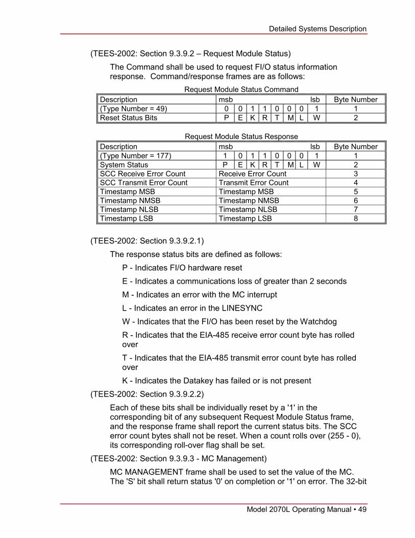
Detailed Systems Description
Model 2070L Operating Manual • 49
(TEES-2002: Section 9.3.9.2 – Request Module Status) The Command shall be used to request FI/O status information response. Command/response frames are as follows:
Request Module Status Command Description msb lsb Byte Number (Type Number = 49) 0 0 1 1 0 0 0 1 1 Reset Status Bits P E K R T M L W 2
Request Module Status Response
Description msb lsb Byte Number (Type Number = 177) 1 0 1 1 0 0 0 1 1 System Status P E K R T M L W 2 SCC Receive Error Count Receive Error Count 3 SCC Transmit Error Count Transmit Error Count 4 Timestamp MSB Timestamp MSB 5 Timestamp NMSB Timestamp NMSB 6 Timestamp NLSB Timestamp NLSB 7 Timestamp LSB Timestamp LSB 8
(TEES-2002: Section 9.3.9.2.1) The response status bits are defined as follows:
P - Indicates FI/O hardware reset E - Indicates a communications loss of greater than 2 seconds M - Indicates an error with the MC interrupt L - Indicates an error in the LINESYNC W - Indicates that the FI/O has been reset by the Watchdog R - Indicates that the EIA-485 receive error count byte has rolled over T - Indicates that the EIA-485 transmit error count byte has rolled over K - Indicates the Datakey has failed or is not present
(TEES-2002: Section 9.3.9.2.2) Each of these bits shall be individually reset by a '1' in the corresponding bit of any subsequent Request Module Status frame, and the response frame shall report the current status bits. The SCC error count bytes shall not be reset. When a count rolls over (255 - 0), its corresponding roll-over flag shall be set.
(TEES-2002: Section 9.3.9.3 - MC Management) MC MANAGEMENT frame shall be used to set the value of the MC. The 'S' bit shall return status '0' on completion or '1' on error. The 32-bit

Section 6 — Theory of Operation
50 • Model 2070L Operating Manual
value shall be loaded into the MC at the next 0-1 transition of the LINESYNC signal. The frames are as follows:
(TEES-2002: Section 9.3.9.4 - Configure Inputs) The Configure Inputs command frame shall be used to change input configurations. The command-response frames are as follows:
Block field definitions shall be as follows:
E - Ignore Input Flag. "1" = do not report transitions for this input, "0" = report transitions for this input
e - A one-byte leading edge filter specifying the number of consecutive input samples which must be "0" before the input is considered to have entered to "0" state from "1" state (range 1 to 255, 0 = disabled)
r - A one-byte trailing edge filter specifying the number of consecutive input samples which must be "1" before the input is considered to have entered to "1" state from "0" state (range 1 to 255, 0 = disabled)
S - return status S = '0' on completion or '1' on error (TEES-2002: Section 9.3.9.5 - Poll Raw Input Data)
The Poll Raw Input Data frame shall be used to poll the FI/O for the current unfiltered status of all inputs. The response frame shall contain

Detailed Systems Description
Model 2070L Operating Manual • 51
8 bytes of information indicating the current input status. The frames are as follows:
Description msb lsb Byte Number (Type Number = 52) 0 0 1 1 0 1 0 0 1
Poll Raw Input Data Response Description msb lsb Byte Number (Type Number = 180) 1 0 1 1 0 1 0 0 1 Inputs I0 (lsb) to I7 (msb) x x x x x x x x 2 Inputs I8 to I63 x x x x x x x x 3 to 9 Timestamp MSB x x x x x x x x 10 Timestamp NMSB x x x x x x x x 11 Timestamp NLSB x x x x x x x x 12 Timestamp LSB x x x x x x x x 13
(TEES-2002: Section 9.3.9.6 - Poll Filtered Input Data) The Poll Filtered Input Data frame shall be used to poll the FI/O for the current filtered status of all inputs. The response frame shall contain 8 bytes of information indicating the current filtered status of the inputs. Raw input data shall be provided in the response for inputs that are not configured for filtering. The frames are as follows:
Poll Filter Input Data Command Description msb lsb Byte Number (Type Number = 53) 0 0 1 1 0 1 0 1 1
Poll Filter Input Data Response
Description msb lsb Byte Number (Type Number = 181) 1 0 1 1 0 1 0 1 1 Inputs I0 (lsb) to I7 (msb) x x x x x x x x 2 Inputs I8 to I63 x x x x x x x x 3 to 9 Timestamp MSB x x x x x x x x 10 Timestamp NMSB x x x x x x x x 11 Timestamp NLSB x x x x x x x x 12 Timestamp LSB x x x x x x x x 13
(TEES-2002: Section 9.3.9.7 - Poll Input Transition Buffer)
The Poll Input Transition Buffer frame shall poll the FI/O for the contents of the input transition buffer. The response frame shall include

Section 6 — Theory of Operation
52 • Model 2070L Operating Manual
a three-byte information field for each of the input changes that have occurred since the last interrogation. The frames are as follows:
(TEES-2002: Section 9.3.9.7.1)
Each detected state transition for each active input (see configuration data) is placed in the queue as it occurs. Bit definitions are as follows:
S Indicates the state of the input after the transition C Indicates the 255 entry buffer limit has been exceeded F Indicates the transition buffer limit has been exceeded G Indicates the requested block number is out of monotonic
increment sequence E Same block number requested, E is set in response
(TEES-2002: Section 9.3.9.7.2) The Block Number byte is a monotonically increasing number incremented after each command issued by the CPU Module. When the FI/O Module receives this command, it shall compare the associated Block Number with the Block Number of the previously received command. If it is the same, the previous buffer shall be re-sent to the CPU Module and the 'E' flag set in the status response frame. If it is not equal to the previous Block Number, the old buffer shall be purged and the next block of data sent. If the block number is not incremented by one, the status G bit shall be set. The block number received becomes the current number (even if out of sequence). The Block Number byte sent in the response block shall be the same as that received in the command block. Counter rollover shall be considered as a normal increment.

Detailed Systems Description
Model 2070L Operating Manual • 53
(TEES-2002: Section 9.3.9.8 - Set Outputs) The Set Outputs frame shall be used to command the FI/O to set the Outputs according to the data in the frame. If there is any error configuring the outputs, the 'E' flag in the response frame shall be set to '1'. If the LINESYNC reference has been lost, the 'L' bit in the response frame shall be set. Loss of LINESYNC reference shall also be indicated in system status information. These command and response frames are as follows:
Set Outputs Command Description msb lsb Byte Number (Type Number = 55) 0 0 1 1 0 1 1 1 1 O0 (lsb) to O7 (msb) Data X x x X x x x x 2 O8 to O63 Data X x x X x x x x 3 to 9 O0 (lsb) to O7 (msb) Control X x x X x x x x 10 O8 to O63 Control X x x X x x x x 11 to 17
Set Outputs Response
Description msb lsb Byte Number (Type Number = 183) 1 0 1 1 0 1 1 1 1 Status 0 0 0 0 0 0 L E 2
(TEES-2002: Section 9.3.9.9 - Configure Input Tracking Functions) The Configure Input Tracking Functions frame shall be used to configure outputs to respond to transitions on a specified input. Each Output Number identified by Item Number shall respond as configured to the corresponding Input Number identified by the same Item Number. Input to Output mapping shall be one to one. If a command results in more than 8 input tracking outputs being configured, the response V bit shall be set to ‘1’ and the command shall not be implemented. The command and response frames are as follows:
(TEES-2002: Section 9.3.9.9.1)

Section 6 — Theory of Operation
54 • Model 2070L Operating Manual
Definitions are as follows: E '1’ - Enable input tracking functions for this output '0' - Disable input tracking functions for this output I '1' - The output is OFF when input is ON, ON when input OFF '0' - The output is ON when input is ON, OFF when input is OFF V '1' - The max. number of 8 configurable outputs has been exceeded '0' - No error
Number of Items - The number of entries in the frame. If zero, all outputs currently configured for input tracking shall be disabled.
(TEES-2002: Section 9.3.9.9.2) The timestamp value shall be sampled prior to the response frame.
(TEES-2002: Section 9.3.9.9.3) Outputs which track inputs shall be updated no less than once per ms. Input to output signal propagation delay shall not exceed 2 ms.
(TEES-2002: Section 9.3.9.9.4) The “Number of Item” field is valid from 0 to 16 (most that is sent at one time is 8 enables and 8 disables). If processing a command resulting in more than 8 Input Tracking functions being enabled, none of the command shall be implemented and response message “V” bit set to 1. If an invalid output or input number is specified for a function, the FIOM software shall not do that function definition. It shall also not be counted toward the maximum of 8 input tracking function allowed. The rest of the message shall be processed. When an Input Tracking function is disabled, the output is set according to the most recently received Set Outputs Command. When an input tracking function for an output is superseded (redefined as either another input tracking function, or as a complex output function) nothing shall be done with the output. The most recent value remains until the new function changes it.
(TEES-2002: Section 9.3.9.10 - Configure Complex Output Functions) CONFIGURE COMPLEX OUTPUT FUNCTIONS - The Configure Complex Output Functions frame shall be used to specify a complex output for one to eight of any of the outputs. If a Configure Complex Output Function command results in more than eight outputs being configured, the 'V' bit in the response message shall be set to a '1', and the command shall not be implemented. Two output forms shall be provided, single pulse and continuous oscillation. These output forms shall be configurable to begin immediately or on a specified input trigger and, in the case of continuous oscillation, to continue until

Detailed Systems Description
Model 2070L Operating Manual • 55
otherwise configured or to oscillate only while gated active by a specified input. If the command gate bit is active, the command trigger bit shall be ignored and the specified input shall be used as a gate signal. The command and response frames are as follows:
(TEES-2002: Section 9.3.9.10.1) The bit fields of the command frame are defined as follows:
E '1' - enable complex output function for this output '0' - disable complex output function for this output J '1' - During the primary duration, the output shall be written as a
logic '1'. During the secondary duration, the output shall be written as a logic '0'.
'0' - During the primary duration, the output shall be written as a logic '0'. During the secondary duration, the output shall be written as a logic '1'.
Output Number - 7-bit output number identifying outputs Primary Duration - For single pulse operation, this shall
determine the number of 'ticks' preceding the pulse. For continuous oscillation, this shall determine the length of the inactive (first) portion of the cycle.
Secondary Duration - For single pulse operation, this shall determine the number of 'ticks' the pulse is active. Subsequent to the secondary duration, the output shall return to the state set according to the most recently received Set Outputs command. For continuous oscillation,

Section 6 — Theory of Operation
56 • Model 2070L Operating Manual
this shall determine the length of the active (second) portion of the cycle. 0 = hold output state until otherwise configured.
F '1' - The trigger or gate shall be acquired subsequent to filtering the specified input. The raw input signal shall be used if filtering is not enabled for the specified input.
'0' - The trigger or gate shall be derived from the raw input. R '1' - For triggered output, the output shall be triggered by an ON-
to-OFF transition of the specified input and shall be triggered immediately upon command receipt if the input is OFF. For gated output, the output shall be active while the input is OFF.
'0' - For triggered output, the output shall be triggered by an OFF-to-ON transition of the specified input and shall be triggered immediately upon command receipt if the input is ON. For gated output, the output shall be active while the input is ON.
Input Number - 7-bit input number identifying inputs 0 Up. P '1' - The output is configured for single-pulse operation. Once
complete, the complex output function shall be disabled. '0' - The output is configured for continuous oscillation. W '1' - It is triggered by the specified input. Triggered complex
output shall commence within 2 ms of the associated trigger. '0' - Operation shall begin within 2 ms of the command receipt. G '1' - Operation shall be gated active by the specified input. '0' - Gating is inactive. L '1' - The LINESYNC based clock shall be used for the time ticks. '0' - The MC shall be used for the time ticks. V '1' - Indicates maximum number of configurable outputs is
exceeded. '0' - No error Number of items - The number of entries in the frame. If 0,
all outputs currently configured as complex outputs shall be disabled.
(TEES-2002: Section 9.3.9.10.2) Controlling input signals shall be sampled at least once per millisecond.
(TEES-2002: Section 9.3.9.10.3)

Detailed Systems Description
Model 2070L Operating Manual • 57
The “Number of Items” field is valid from 0 to 16. Zero means disable all Complex Output functions. Sixteen is the maximum because the most that is sent at one time is 8 enables and 8 disables. If processing a command results in more than 8 Complex Output functions being enabled, none of the command shall be implemented and the response message “V” bit shall be set to 1. If an invalid output or input number (the “G” or “W” bits being set to 1 is specified for a function, that function definition is not done by the FIOM software. It shall also not be counted towards the maximum of 8 Complex Output functions allowed. The rest of the message shall be processed. When a Complex Output function is disabled, the output is set according to the most recently received Set Outputs command. When a complex output function for an output is superseded, that is, redefined as wither another Complex Output function, or as an Input Tracking function, nothing special is done with the output. The most recent value remains until the new function changes it. The “G” bit (gating) set to 1 takes precedence over the “W” bit (triggering). If gating is ON, triggering is turned OFF, regardless of the value of the “W” bit in the command message. If a Complex Output is configured with the “G” bit set to 1 (gating) and the “P” bit set to 0 (continuous oscillation), the output is set to OFF (0) whenever the specified input changes state so that the oscillation should cease (output inactive). For a single pulse operation (“G” bit set to 1), after the secondary duration completes the Complex Output function shall be disabled, and the output shall be set according to the most recently received Set Outputs command.
(TEES-2002: Section 9.3.9.11 - Configure Watchdog) The Configure Watchdog frames shall be used to change the software watchdog timeout value. The Command and response frames are as follows:
(TEES-2002: Section 9.3.9.11.1)
The timeout value shall be in the range between 10 to 100 ms. If the value is lower than 10, 10 shall be assumed. If the value is greater than 100, 100 shall be assumed.
(TEES-2002: Section 9.3.9.11.2)

Section 6 — Theory of Operation
58 • Model 2070L Operating Manual
On receipt of this frame, the watchdog timeout value shall be changed to the value in the message and the “Y” bit set. The response frame bit (Y) shall indicate a '1' if the watchdog has been previously set and a '0' if not.
(TEES-2002: Section 9.3.9.12 - Controller Identification) This is a legacy message command / response for FI/O modules with Datakey resident. Upon command, a response frame containing the 128 bytes of the Datakey. On NRESET transition to High or immediately prior to any interrogation of the Datakey, the FI/O shall test the presence of the Key. If absent, the FI/O Status Bit “K” shall be set and no interrogation shall take place. If an error occurs during the interrogation, Bit “K” shall be set. If “K” bit set, only the first two bytes shall be returned. The Command Response frames are as follows:
(TEES-2002: Section 9.3.9.13 - Module Identification) The FI/O Identification command frame shall be used to request the FI/O Identification value Response of “1” for 2070-2A. The command and response frames are shown as follows:
6.2.5 Display Module The 2070-3B display module provides the 2070L with its physical user interface, including an LCD screen and dual keypad inputs. The display is attached to the chassis via the chassis’ hinge, and to the chassis motherboard via the chassis’ J1 ribbon cable.

Detailed Systems Description
Model 2070L Operating Manual • 59
Figure 22 – Display Module block diagram There are basically four sections of the display module’s operation: the LCD display, the front panel controls, the microcontroller and associated logic, and the connectors. The connectors are comprised of a J1 ribbon cable which connects the display module to the chassis (and through that to the CPU and the rest of the controller,) and a front-panel C50S serial connector. The ribbon cable provides two RS485 serial comms channels (SP4 and SP6), several TTL-logic status lines, and power from the chassis. SP4 connects to the C50S connector. SP6 provides data flow between the front panel microcontroller and the 2070L’s CPU. The microcontroller operates as the ‘brain’ of the display interface, routing display elements to the LCD, keypad inputs to the screen and the CPU, and routing CPU data to the display. The micro reads the status of eight factory-preset links that function as the Config for the display, telling the controller what type of LCD and keypad are installed. The micro uses the two memory locations (EPROM and SRAM) to store its internal application and data to be displayed on the LCD. The data is transferred by the micro to memory and to the LCD across a data bus. The LCD is driven by the microcontroller using the data bus and an LCD control channel. The LCD itself has a backlight and a contrast setting. The contrast setting is set using the front panel Contrast knob. This contrast knob is connected to a variable resistor that directly controls the LCD setting, so it is possible to inadvertently turn this all the way down or up and not be able to read the display. The LCD’s backlight is activated by the microcontroller whenever the keypad is pressed.

Section 6 — Theory of Operation
60 • Model 2070L Operating Manual
The other front panel controls have a variety of functions, some of which interact through the microcontroller, and others that do not. The Buzzer, AUX Switch and Keypads all interact with the micro. The buzzer is sounded whenever the unit is reset, as well as in the case of an error. The state of the AUX switch is detected by the microcontroller in the display module, but it is immediately passed through the J1 cable to the CPU, in the form of the AUX Switch Code. The function of the AUX code depends on the software that has been loaded into the 2070L by the operator. The characters from the keypads are handled both locally by the microcontroller, and passed along to be processed by the CPU. The other controls are not handled by the microcontroller. The contrast knob, as we said, connects directly with the LCD. The ACTIVE LED on the front panel connects, via the J1 cable, to the CPU LED signal. Finally, the Board Reset Generator takes inputs from two possible sources: a CPU_RESET signal coming from the chassis will cause the display board to reset, or the user can press the push button located on the rear of the display module, on the side of the display’s lower PCB. It is important to remember, however, that the reset button will only reset the display board, not the whole 2070 unit. (For that, you will need to turn the power off and on for a couple of seconds.)
TEES Compliance The Quixote 2070-3B Display module also functions as described in the CalTrans requirements, as stated in the following sections of the August 16, 2002 TEES document: (TEES-2002: Section 9.4.4.3)
Cursor display shall be turned ON and OFF by command. When ON, the cursor shall be displayed at the current cursor position. When OFF, no cursor shall be displayed. All other cursor functions (positioning, etc.) shall remain in effect.
(TEES-2002: Section 9.4.5.1) A FPA RESET Switch shall be provided on the Assembly PCB. The momentary CONTROL switch shall be logic OR'd with the CPU RESET Line, producing a FPA RESET Output. Upon FPA RESET being active or receipt of a valid Soft Reset display command, the following shall occur:
1. Auto-repeat, blinking, auto-wrap, and auto-scroll shall be set to OFF.
2. Each special character shall be set to ASCII SPC (space). 3. The tab stops shall be set to columns 9, 17, 25, and 33. 4. The backlight timeout value shall be set to 6 (60 seconds). 5. The backlight shall be extinguished. 6. The display shall be cleared (all ASCII SPC).

Detailed Systems Description
Model 2070L Operating Manual • 61
7. The FPA module shall transmit a power up string through /sp6 to the CPU once power is applied to the FPA, or the FPA hardware RESET BUTTON IS PUSHED. The string is “ ESC [ PU”, hex value “1B 5B 50 55”.
(TEES-2002: Section 9.4.5.2) When a key press is detected, the appropriate key code shall be transmitted to SP6-RxD. If two or more keys are depressed simultaneously, no code shall be sent. If a key is depressed while another key is depressed, no additional code shall be sent.
(TEES-2002: Section 9.4.5.3) Auto-repeat shall be turned ON and OFF by command. When ON, the key code shall be repeated at a rate of 5 times per second starting when the key has been depressed continuously for 0.5 second, and shall terminate when the key is released or another key is pressed.
(TEES-2002: Section 9.4.5.4) When the AUX Switch is toggled, the appropriate AUX Switch code shall be transmitted to the CPU.
(TEES-2002: Section 9.4.5.5) The controller circuitry shall be capable of composing and storing eight special graphical characters on command, and displaying any number of these characters in combination with the standard ASCII characters. Undefined characters shall be ignored. Usercomposed characters shall be represented in the communication protocol on Page 9-7-12. P1 represents the special character number (1-8). Pn's represent columns of pixels from left to right. The most significant bit of each Pn represents the top pixel in a column and the least significant bit shall represent the bottom pixel. A logic ‘1’ shall turn the pixel ON. There shall be a minimum of 5 Pn's for 5 columns of pixels in a command code sequence terminated by an "f." If the number of Pn's are more than the number of columns available on the LCD, the extra Pn's shall be ignored. P1 and all Pn's shall be in ASCII coded decimal characters without leading zero.
(TEES-2002: Section 9.4.5.6) Character overwrite mode shall be the only display mode supported. A displayable character received shall always overwrite the current cursor position on the Display. The cursor shall automatically move right one character position on the Display after each character write operation. When the rightmost character on a line (position 40) has been overwritten, the cursor position shall be determined based on the current settings of the auto-wrap mode.
(TEES-2002: Section 9.4.5.7)
Section 6 — Theory of Operation
62 • Model 2070L Operating Manual
Auto-wrap shall be turned ON & OFF by command. When ON, a new line operation shall be performed after writing to position 40. When OFF, upon reaching position 40, input characters shall continue to overwrite position 40.
(TEES-2002: Section 9.4.5.8) Cursor positioning shall be non-destructive. Cursor movement shall not affect the current display, other than blinking the cursor momentarily and periodically hiding the character at that cursor position.
(TEES-2002: Section 9.4.5.9) Blinking characters shall be supported, and shall be turned ON and OFF by command. When ON, all subsequently received displayable characters shall blink at the rate of 1 Hz with a 60% ON / 40% OFF duty cycle. It shall be possible to display both blinking and non-blinking characters simultaneously.
(TEES-2002: Section 9.4.5.10) Tab stops shall be configurable at all columns. A tab stop shall be set at the current cursor position when a SetTabStop command is received. Tab Stop(s) shall be cleared on receipt of a ClearTabStop command. On receipt of the HT (tab) code, the cursor shall move to the next tab stop to the right of the cursor position. If no tab stop is set to the right of the current cursor position, the cursor shall not move. Tab stops shall be set based only upon the column (horizontal) position of the cursor; the row position shall be ignored. Each tab that is set shall be applied to all rows of the display. In this way, tabs shall operate similarly to a typewriter or line printer. For example, if the cursor is positioned at column 21, row 3 when a Set Tab Stop command (ESC H) is received, a tab stop is placed at column 21 and applies to every row of the display. If the cursor is then positioned to column 21, row 5, and a Clear Tab Stop command (ESC[0g) is received, the tab stop on column 21 is removed and there will be no tab stop on any row of the display at that column position.
(TEES-2002: Section 9.4.5.11) Auto-scroll shall be turned ON and OFF by command. When ON, a Line Feed or new line operation from the bottom line shall result in the display moving up one line. When OFF, a Line Feed or new line from the bottom line shall result in the top line clearing, and the cursor being positioned on the top line.
(TEES-2002: Section 9.4.5.12) Displayable characters shall be refreshed at least 20 times per second.
(TEES-2002: Section 9.4.5.13)
Detailed Systems Description
Model 2070L Operating Manual • 63
The Display back light shall illuminate when any key is pressed and shall illuminate orextinguish by command. The backlight shall extinguish when no key is pressed for a specified time. This time shall be program selected by command, by a number in the range 0 to 63 corresponding to that number of 10-second intervals. A value of 1 shall correspond to a timeout interval of 10 seconds. A value of 0 shall indicate no timeout.
(TEES-2002: Section 9.4.5.14) The Command Codes shall use the following conventions:
1. Parameters and Options: Parameters are depicted in both the ASCII and hexadecimal representations as the letter 'P' followed by a lower-case character or number. These are interpreted as follows:
Pn: Value parameter, to be replaced by a value, using one ASCII character per digit without leading zeros.
P1: Ordered and numbered parameter. One of a listed known parameters with a specified order and number (Continues with P2, P3, etc.)
Px: Display column number (1-40), using one ASCII character per digit without leading zero.
Py: Display line (1-4) one ASCII character ... : Continue the list in the same fashion Values of 'h' ($68) and 'l' ($6C) are used to indicate binary
operations. 'h' represents ON (high), 'l' represents OFF (low). 2. ASCII Representation: Individual characters are separated by
spaces; these are not to be interpreted as the space character, which is depicted by SPC.
3. Hexadecimal Representation: Characters are shown as their hexadecimal values and will be in the range 00 to 7F (7 bits).
(TEES-2002: Section 9.4.5.15) The Controller Circuit shall communicate via a SP6 asynchronous serial interface. The interface shall be configured for 38.4 Kbps, 8 data bits, 1 stop bit, and no parity.
(TEES-2002: Section 9.4.5.16) C50 ENABLE function when grounded by Connector C50 Pins 1 and 5 shall be brought to Connector A1 Pin B21 for the purpose of disabling the module Channel 2.
(TEES-2002: Section 9.4.6)
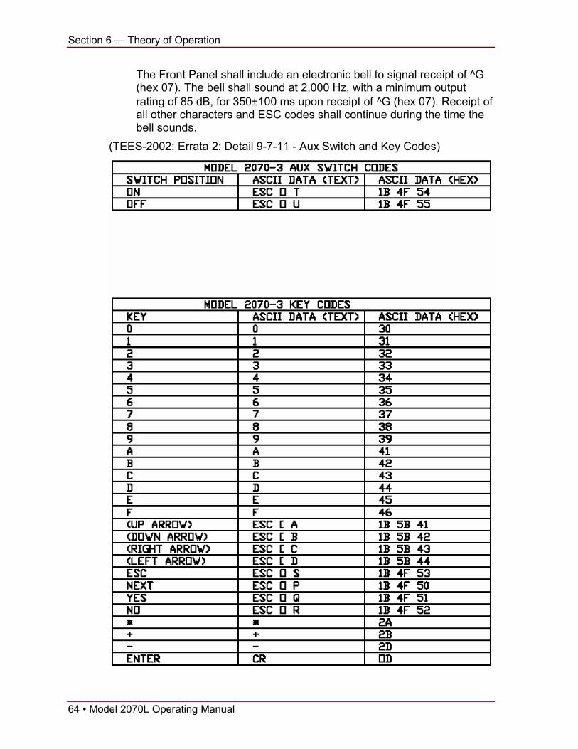
Section 6 — Theory of Operation
64 • Model 2070L Operating Manual
The Front Panel shall include an electronic bell to signal receipt of ^G (hex 07). The bell shall sound at 2,000 Hz, with a minimum output rating of 85 dB, for 350±100 ms upon receipt of ^G (hex 07). Receipt of all other characters and ESC codes shall continue during the time the bell sounds.
(TEES-2002: Errata 2: Detail 9-7-11 - Aux Switch and Key Codes)

Detailed Systems Description
Model 2070L Operating Manual • 65
(TEES-2002: Errata 2: Detail 9-7-12 - Configuration Command Codes, Inquiry Command-Response Codes )

Section 6 — Theory of Operation
66 • Model 2070L Operating Manual
6.2.6 Power Supply Module The Quixote 2070-4A and 4B power supply modules are identical except for the silkscreen on the metalwork. The 2070-4 power supply module takes 120VAC line power as an input and provides DC power and several logical outputs to the other modules of the 2070L. The power supply’s operation can be basically divided into two parts: the power switcher and the monitoring logic.
Figure 23 – Power Supply block diagram AC line voltage comes into the module through an AC fuse, line protection and AC filtering, where it is fed to an AC-to-high-voltage-DC switcher, and from there to a DC-DC switcher. This set of voltage switchers provide the 2070L modules with isolated +12V DC, serial plus and minus 12 VDC, and

Detailed Systems Description
Model 2070L Operating Manual • 67
+5 VDC. The switching section of the circuit monitors both internal and external +5VDC power points to automatically adjust operation in the high voltage DC switcher. The monitoring portion of the circuit centers on the LPC2131 microcontroller, which performs several monitoring and status output functions for the 2070L. First, the micro monitors the 60Hz frequency of the AC line voltage, and uses it to generate a 30 degree phase shifted 60 Hz signal which is sent out on the LINESYNC channel to all of the other modules in the controller. If the micro detects that AC Power In has gone down, it steps in and, while the circuit is held up by brownout power, generates the LINESYNC signal on its own, at the last known frequency that was detected at AC Power In. At this basic level, the microcontroller also monitors AC Power In to generate a set of logical signals out on the POWERDOWN, POWERUP, AC FAIL, and SYSRESET channels. AC FAIL and SYSRESET are essentially duplicates of POWERDOWN and POWERUP, only directed specifically to the VME module, should one be installed in the 2070 chassis. POWERDOWN and POWERUP are generated by the microcontroller to indicate to the CPU and other modules of the controller when the power supply has detected a problem with AC power. These function as a two stage warning system to the rest of the circuitry. POWERDOWN indicates that a brown out has occurred, meaning that AC Power In has dropped below 92 volts for more than 50 milliseconds. The 2070L can recover from this situation without going through any restart procedure as long as power is restored to above 97 volts within approximately a half second. But if power stays low for more than this time, the POWERUP indicator is also triggered. When POWERUP is triggered, it indicates to the CPU and other modules that a full restart will need to occur. Since both POWERUP and POWERDOWN are fail states, they are normally held high to indicate when things are peachy-keen, but transition to 0V (low) to indicate a problem. (So, when the power supply loses power completely, both of these signals automatically switch to their ‘problem’ states of 0V. If the other modules of the controller see that POWERUP is in the low state, then when power is restored they will awaken into their power up procedures, hence the name of this fault channel.) The microcontroller also monitors the state of the DC voltages that are being generated by the power supply (+5V, +/-12V, +12V Iso), and displays the health of those voltages on a set of LED indicators located on the front panel of the power supply unit. These LEDs indicate the health of the conditioned power as delivered to the Power Supply’s front panel PS1 and PS2 connectors. Each of these LEDs glows red as long as the power on that channel is within 2070 specifications. (See Table 2 on page 16 for those voltage ranges.) If the power on these outputs goes anywhere outside of the specified range, the associated LED is switched OFF by the microcontroller. It remains off until the power returns to the desired range.

Section 6 — Theory of Operation
68 • Model 2070L Operating Manual
But what happens to this circuit when AC power is removed (either by the utility going down, or the main power switch being turned off?) The 2070 specification defines how this is handled, and the Quixote 2070L meets and usually exceeds those requirements. In normal operation, the AC-to-High-Voltage DC switcher and the DC-to-DC switcher both feed power to an auxiliary supply that runs their internal circuitry; the circuitry that actually performs the power transformation. When AC power is removed, a large capacitor at the output of the AC-to-High-Voltage DC switcher keeps all of the circuits to the right of it powered up for a short time. This is what gives the 2070 its ability to ‘bridge’ over short power interrupts. When such a brown-out occurs, the DC-to-DC switcher keeps operating, fed by this large capacitor. In this state, the DC-to-DC switcher keeps the auxiliary supply powered up for its own operation for as long as power remains in the circuit. While the DC-to-DC switcher is running, it will maintain the output voltages. By design, it can keep a nominal 30 watts supplied (on all of the outputs combined) for approximately 600 milliseconds. These are typical values for a normally outfitted 2070L controller. If additional components have been added to the chassis, this time will be shorter. And since the DC-to-DC switcher keeps the +5V line up during such an event, this also provides power to the microcontroller so that it can continue to perform its monitoring and signal output functions across a short power outage. The +5V Standby output is sent over the backplane to the motherboard, where it supplies backup power to the Real-time Clock. When the 2070L is disconnected from AC for extended periods, a set of large capacitors provide power to the +5V Standby line for up to several weeks. One last note about the power supply operation concerns the 5V Sensor Input, and the 5V Feedback and External 5V Sense parts of the block diagram. The Sensor Input is provided to monitor the +5V voltage within an optionally installed VME chassis. The Feedback component monitors both this ‘external’ signal and the output of the switcher’s own +5V output to verify that it is generating the proper output. All of the DC outputs from the switcher are ganged off of this feedback circuit, so if the +5V output is detected to be low, the power supply will raise its output into the proper range for the +5V channel and would raise the other three DC outputs. To ensure proper regulation of the three 12V outputs, each of these voltages has a “post regulator” that governs the actual voltage levels. The three 12V outputs are also power-conditioned with over-voltage protection before being sent to the PS1 and PS2 connectors.

Detailed Systems Description
Model 2070L Operating Manual • 69
6.2.7 Async Serial Module A 2070-7A Async Serial Module provides two channels of asynchronous communications between the 2070L and the external world. The operation of the Async Serial module is illustrated below.
Figure 24 – Async Serial Module block diagram The module takes two channels of RS485 communications from the backplane (SP1 and 2 if the module is installed in slots A2-A4, SP3 and 4 if the module is installed in slot A1) and provides it to two RS232 DE9 ports on its front panel. These ports, C21S and C22S, are optically isolated on both data and power lines from the backplane of the 2070L. Both channels provide full handshaking capability. The C50 ENABLE line, which comes in from the backplane, tells the module whether or not to enable channel 2 (the bottom port.) If the C50 port on the front of the Display module is enabled, it normally uses SP4 for communications. To avoid a communications conflict, if the C50 ENABLE is ON, then channel 2 on this card is disabled. The C50 ENABLE signal is only used by this card if the card is installed in slot A1. (No conflict occurs between this module’s channel 2 and the Display module’s C50 port if the card is installed in any of the other slots, since they all assign channel 2 to use the SP2 serial port.) The TX and RX LEDs on the front face of the Async Serial module are simple TTL displays of the state of those lines for each of the RS232 ports.

Section 6 — Theory of Operation
70 • Model 2070L Operating Manual
Model 2070L Operating Manual • 71
7 Maintenance 7.1 Preventive Maintenance
Routine general maintenance should be performed on the controller in the field whenever a technician has the need to access the unit on-site. Simply ensure that the ventilation slots are free from dust and that all plug-in modules are firmly seated in the chassis. Also verify that the cables running between the chassis and the Display module are firmly attached and undamaged.
7.2 Trouble Analysis
7.2.1 Field Diagnosis Should a Quixote 2070 controller exhibit erratic behavior or fail in the field, it should be replaced and sent to the repair shop with appropriate notes describing the symptoms.
7.2.2 Laboratory Diagnosis Testing the Quixote 2070 in a lab setting usually involves loading and running a 2070 Diagnostics and Test (DAT) utility. This 2070 DAT utility is normally loaded to the memory of the 2070 using a Windows-based PC that is attached to the unit by a serial cable plugged into the C50S port on the front of the unit. It is designed to test the functionality of all of the installed modules of the Quixote 2070 controller. For setup procedures, peripheral equipment requirements, and operating instructions, refer to the 2070 DAT manual.
7.2.3 Hardware Failure Diagnosis Should a 2070 controller fail to operate at all with the 2070 DAT utility, further analysis of the hardware must be performed by checking all power supply voltages, viewing waveforms, clock signals, power up and down timing circuits, etc.
7.3 Troubleshooting Sequence Chart When a problem occurs with a 2070 controller, proceed through the following three-teir diagnostic check system until the problem is identified.
7.3.1 Preliminary Checks The following preliminary checks should be done before more extensive troubleshooting is performed: 1. Adjust the Contrast knob on the front panel Display module so it is in the
middle of its setting range. 2. Check the fuse located in the power supply.

Section 7 — Maintenance
72 • Model 2070L Operating Manual
3. Ensure that all modules are properly installed and firmly seated in their connectors. Make sure all retaining screws are in place and tightened.
4. Ensure that all cable connections are correctly mated at each end and, where appropriate, make sure that cable retaining screws are in place and tightened.
5. Check that the 2070 controller has a valid software program installed. 6. If a terminal connection is being used to operate or diagnose the
controller, ensure that the cabling used to connect to the controller is properly connected, and that the port is set to the appropriate baud rate, word length, and parity.
7.3.2 Power Supply Checks Use a digital voltmeter to test the power supply voltages at the PS1 and PS2 pin outputs. These voltages should measure steadily within the limits shown in Table 2 on page 16.
7.3.3 Further Troubleshooting Further checks may be carried out, but only by qualified and experienced technicians, using digital voltmeters and oscilloscopes in conjunction with the schematic diagrams and descriptions provided within this manual.
7.4 Wave Forms There are no critical wave forms required for the troubleshooting of the Quixote 2070 controller.
7.5 Voltage Requirements The required voltage outputs of the 2070 power supply, and the power and current requirements of the other 2070 modules are described in Table 2 and Table 3 on page 16.
7.6 Alignment Procedures There are no alignment procedures required to operate the Quixote 2070 Controller.

Index
Model 2070L Operating Manual • 73
Index 2070 DAT..............................................71 2070L
front view ............................................5 power on ...........................................21 rear view ...........................................10
210 monitor unit ....................................28 210ACTIVE ...........................................42 3U ...........................................................1 6 Series.................................................35 6U ...........................................................1 7 Series.................................................35 A# connectors .......................................33 A# port usage........................................35 A1 comms signals .................................33 A1 connector.........................................33 A2 INSTALLED .....................................37 A2-A5 comms signals............................33 A3 INSTALLED .....................................37 AC...........................................................1 ACFAIL .......................................1, 16, 67 ADDR......................................................1 adjustments...........................................27
display module ..................................28 electrical............................................27 mechanical........................................27 SP3...................................................27
ANSI .......................................................1 async ......................................................1 async comm module
installation.........................................25 async module
LEDs.................................................70 async serial module...................12, 21, 70 ATC.........................................................1 ATC connector ......................................41 ATC engine board .................................37 auto recovery ........................................16 AUX ......................................................35 aux switch .............................................60 baud........................................................1 BERR......................................................1 block diagram
async module....................................70 chassis..............................................33 CPU ..................................................37 display module ..................................59 engine board.....................................41 field I/O module.................................42
power supply.....................................67 board reset generator............................60 boot and apps flash ...............................41 brown out ..............................................69 buffers ...................................................42 bus ......................................................... 1 bus control line mapping........................39 buzzer ...................................................60 C11S connector...........................8, 20, 42 C12S connector........... 5, 8, 21, 27, 35, 42 C13S connector...........................7, 37, 39 C14S connector.....................................21 C1S connector ............................8, 20, 42 C21S connector...............................21, 70 C22S connector.........................14, 21, 70 C50 enable............................................70 C50S connector...............................36, 59 cabinet ................................................... 1
connection 2070 to............................20 ITS type.............................................. 8 Type 332............................................ 8
cabinet harness.....................................20 CD.......................................................... 1 chassis ..............................................6, 17
adjustments.......................................27 block diagram..............................31, 33 theory of operation ............................32
circuit protection ....................................16 clock......................................................39 cold start ...............................................16 collision .................................................37 comms modules ....................................35 communications ....................................40 compliance........................................5, 15 conflict
SP4 ...................................................36 conflict monitor ......................................43 connecting power ..................................21 connector labelling ................................. 5 connectors
A1 .....................................................33 A2-A5................................................33 C11S.......................................8, 20, 42 C12S...........................8, 21, 27, 35, 42 C13S...........................................37, 39 C14S.................................................21 C1S.........................................8, 20, 42 C21S...........................................21, 70

Index
74 • Model 2070L Operating Manual
C22S .................................... 14, 21, 70 C50S ..........................................36, 59 FP.....................................................34 PS1...................................................69 PS2...................................................69
contrast .................................................28 cooling ..................................................20 CPU........................................................1
block diagram ...................................37 host board.........................................37 installation.........................................22
CPU module ...........................................7 CPU reset .............................................43 CTS ..................................................1, 33 current
input..................................................15 inrush..........................................15, 16
current draw CPU....................................................7
DataKey........................................ 1, 7, 37 DC ..........................................................1 DC to DC switcher ................................67 DCD......................................................33 display module ..................................9, 59
adjustments ......................................28 installation.........................................23
DRAM ......................................... 1, 39, 41 DSP ......................................................42 dual port RAM.................................42, 43 DUART ..................................... 39, 40, 41 EEPROM ..............................................37 efficiency...............................................16 EIA..........................................................1 EIA-232...................................................2 EIA-485...................................................2 electrical adjustments............................27 electrostatic discharge ..........................17 engine board.........................................39 environmental requirements..................15 EPROM....................................... 2, 42, 60 ESD ......................................................17 Ethernet .................................... 21, 37, 40 Ethernet LEDs.........................................7 Eurocard .................................................3 Field I/O module......................................8
installation.........................................22 flash ..................................................2, 41 FLE210P...............................................42 FP...........................................................2 FP connector ........................................34 fuse.................................................24, 37
general description..................................5 glossary ..................................................1 GND........................................................2 GPS/Comms module ............................14 grounding the unit .................................20 handling ................................................19 hardware failure diagnosis ....................71 hardware inspection ..............................19 heat issues............................................19 holdup time ...........................................16 host board.............................................37 humidity range ......................................15 Hz ...........................................................2 I/O...........................................................2 I/O control .............................................43 ICC .........................................................2 IEEE........................................................2 IMP .........................................................2 input buffers ..........................................42 input current ..........................................15 input voltage..........................................15 inrush current ..................................15, 16 installation
async comm module .........................25 async serial module ..........................21 attaching cabinet harness .................20 CPU into chassis...............................22 display module..................................23 Field I/O module................................22 grounding..........................................20 heat...................................................19 humidity ............................................19 overview ...........................................19 physical install in cabinet...................19 power supply.....................................24
interrupt.............................................2, 40 IRQ .........................................................2 IRQ210P ...............................................42 isolation.................................................37 ITS ..........................................................8 J1 59 jumpers .................................................27 keypad ..................................................60 laboratory diagnosis ..............................71 LCD...............................................2, 9, 59
temperature limits .............................15 LED.........................................................2 LEDs
CPU front panel ................................37 CPU module .......................................7 POSFIX ............................................14

Index
Model 2070L Operating Manual • 75
power condition...................................9 RX...............................................12, 14 SP3 Active ..........................................8 TX ...............................................12, 14
line regulation........................................16 LINESYNC ................ 2, 33, 39, 42, 43, 67 load regulation.......................................16 LPC2131 ...............................................68 LSB .........................................................2 M104.....................................................20 magnetics..............................................41 maintenance .........................................71 MC68302 ....................................2, 40, 42 MC68360 ..............................2, 39, 40, 41 memory.................................................39 microcontroller.................................39, 40 microprocessor......................................42 MIL-STD..................................................2 mm........................................................39 model 210 conflict monitor ....................43 module ....................................................3
async serial .......................................12 CPU ....................................................7 display.................................................9 Field I/O ..............................................8 GPS/Comms.....................................14 power specifications..........................17 power supply.......................................9 synchronous serial ............................14
motherboard............................................3 Motorola MC68360..................................7 MOV........................................................3 MSB ........................................................3 muzzle jumper.................................27, 28 noise .....................................................16 NReset ............................................42, 43 NRESET ...............................................39 ohm.........................................................1 opto isolation.........................................14 output buffers ........................................42 over voltage protection ..........................16 overview
serial ports ........................................35 PCB ........................................................3 PHY ................................................40, 41 plug .......................................................10 port 2 enable .........................................70 port conflict............................................36 ports
serial channels ..................................34 POSFIX.................................................14
power connecting.........................................21 frequency specs................................15 monitoring .........................................68 regulation ..........................................16 tolerances .........................................16
power cord ............................................10 power down...........................................40 POWER DOWN ..............................33, 67 power lines ............................................34 power loss
holdup time .......................................16 power regulation....................................69 power specifications ..............................15 power supply .........................................67
installation .........................................24 troubleshooting..................................72
power supply module ............................. 9 output requirements ..........................15
power up ...............................................40 POWER UP.....................................33, 67 powering on...........................................21 preliminary checks.................................71 preventative maintenance .....................71 PS1 ........................................................ 9 PS1 connector.......................................69 PS2 ........................................................ 9 PS2 connector.................................10, 69 rack mounting........................................19 RAM....................................................... 3 real-time clock .................................39, 69 receive ..................................................37 regulated power.....................................16 regulation of power................................69 remove sense........................................16 reset generator......................................41 reset management ................................40 reset out ................................................40 ripple .....................................................16 RJ45......................................................37 ROM....................................................... 3 routing
wiring ................................................21 RST210P...............................................42 RTC...........................................39, 40, 41 RTS...................................................3, 33 RTS1.....................................................42 RX...................................3, 12, 14, 33, 70 RXC ......................................................33 S1 switch...............................................43 SDLC ..................................................... 3

Index
76 • Model 2070L Operating Manual
sensor input ..........................................69 serial peripheral interface......................39 serial port operation ..............................35 serial ports ............................................34 setting the muzzle jumper .....................28 SIU modules .........................................21 SP channels..........................................33 SP3.......................................................35 SP3 active LED.....................................43 SP3 Active LED ......................................8 SP3 ENABLE........................................42 SP3 ON.................................................27 SP4.......................................................35 SP4 port conflict....................................36 SP8.......................................................39 specifications
power................................................15 SRAM ....................... 3, 39, 40, 41, 42, 60 standards compliance .......................5, 15 static discharge.....................................17 status ....................................................37 STBY ......................................................3 SYNC......................................................3 synchronous serial module....................14 SYSCLK..................................................3 SYSFAIL.................................................3 SYSRESET.......................................3, 67 system overview .....................................5 TEES ............................................ 3, 5, 15
temperature range.................................15 theory of operation ................................31 time
power holdup ....................................16 transient response.................................16 Transition Board................................7, 35 transmit .................................................37 troubleshooting .....................................71 TTL .........................................................3 TX ................................... 3, 12, 14, 33, 70 TXC...................................................3, 33 TXCI......................................................33 TXCO....................................................33 TXD.........................................................3 USB ............................................7, 37, 41 VAC ........................................................3 VBB.........................................................3 VCC ........................................................3 VDC ........................................................3 VME..................................................3, 35 VME chassis .....................................7, 69 voltage
input..................................................15 overshoot ..........................................16
VOUT................................................3, 16 watchdog ........................................41, 42 watchdog signal ....................................28 wire routing ...........................................21


Quixote Traffic, Inc.2511 Corporate WayPalmetto, FL 34221ph: (941) 845-1200in U.S.:fx:web: www.quixtraffic.com
(800) 245-7660(941) 365-0837
81-1126
A Company