quick reference user guide for analog peripherals on...
TRANSCRIPT
Freescale SemiconductorQuick Reference User GuideAbstract
Document Number: ANPERIPHQRUGRev. 0, 07/2010
Contents
Introduction . . . . . . . . . . . . . . . . . . . . . . . . . . . . . . . . . . . 1Using VREF module on MM and JE devices. . . . . . . . . . 3PDB module for MM and JE devices. . . . . . . . . . . . . . . . 8ADC module for MM devices. . . . . . . . . . . . . . . . . . . . . 14Op-amp Module for MM devices . . . . . . . . . . . . . . . . . . 29TRIAMP for MM devices . . . . . . . . . . . . . . . . . . . . . . . . 38DAC for MM and JE devices . . . . . . . . . . . . . . . . . . . . . 39Differential Input – Single Output. . . . . . . . . . . . . . . . . . 45Differential Input – Differential Output advantages . . . . 51
0 References . . . . . . . . . . . . . . . . . . . . . . . . . . . . . . . . . . 541 Revision History. . . . . . . . . . . . . . . . . . . . . . . . . . . . . . . 54
Quick Reference User Guide for Analog Peripherals on the MM and JE Familyby: Alejandra Guzman, Wang Hao, Han Lin, Carlos Neri, Medina Rimoldi Cuauhtemoc
1 IntroductionThe Flexis™ MM and JE series provides all the integrated analog peripherals that is needed to make user application perform as a breakthrough medical design. Integrated 16-bit ADC, 12-bit DAC, op-amps, Transimpedance amplifiers and USB connectivity make the Flexis™ MM and JE ideal for medical applications.
This document is intended to provide a quick reference to start using the analog peripherals in the Flexis™ MM and JE series. The document provides a peripheral overview, tips on peripheral initialization, code snippets and real use cases.
This document covers the “measurement engine”, the group of analog peripherals included in the Flexis™ MM and JE series. Following connections can be made within the measurement engine to improve its efficiency:
• The 16-bit successive approximation ADC can be configured to have an external, internal or alternate voltage reference
12345678911
© Freescale Semiconductor, Inc., 2010. All rights reserved.

Introduction
• The ADC can also be connected to the op-amp inputs and outputs and to the 12-bit DAC. The DAC outputs can be connected to external pins or the 16-bit SAR ADC.
• Both the transimpedance and general purpose op-amp module inputs can be configured either from external pin inputs or the voltage level provided by the DAC module.
• The VREF module can provide VREFH to the DAC and ADC. It also supplies an accurate voltage output that is trimmable by an 8-bit register. The voltage reference can be used to provide a reference voltage to external peripherals or as a reference to analog peripherals like the ADC or analog comparator.
NOTEThe op-amps and triamps are only available in the Flexis™ MM family. The Flexis™ JE family features a 12-bit ADC and the Flexis™ MM family features a 16-bit ADC.
Quick Reference User Guide for Analog Peripherals on the MM and JE Family, Rev. 0
Freescale Semiconductor2

Using VREF module on MM and JE devices
2 Using VREF module on MM and JE devices
2.1 OverviewThis is a quick reference for using the voltage reference module on MM family MCUs. The VREF is intended to supply an accurate constant (fixed) voltage output as a reference for on-chip analog peripherals or off-chip external peripherals.
On-chip peripherals that use VREF include ADC, DAC, and PRACMP (Programmable Analog Comparator) peripherals. Off-chip peripherals can get VREF output signal via the VREFO (Voltage Reference Output) pin.
Conventional bandgap voltage reference has a larger deviation over process variation, temperature, and voltage. This VREF allows corrective trimming to improve accurate reference voltage. In MM devices, the target output for this output reference voltage is at 1.15V. A trim register is provided for user to trim the VREF output voltage to as close to as 1.15V. Note that production MM devices should have VREF output trimmed to 1.15V out of factory.
Figure 1 shows on-chip analog peripherals that have the option to use VREF output reference.
Figure 1. Using VREF module on MM and JE devices
2.2 VREF peripheral features• Programmable trim register with 0.5 mV steps, automatically loaded with room temperature value
upon reset• Programmable mode selection:
Quick Reference User Guide for Analog Peripherals on the MM and JE Family, Rev. 0
Freescale Semiconductor 3
Using VREF module on MM and JE devices
— Off— Bandgap out (or stabilization delay)— Low power buffer mode— Tight-Regulation buffer mode
• 1.15 V output at room temperature, 40 ppm/C• Dedicated output pin, VREFO
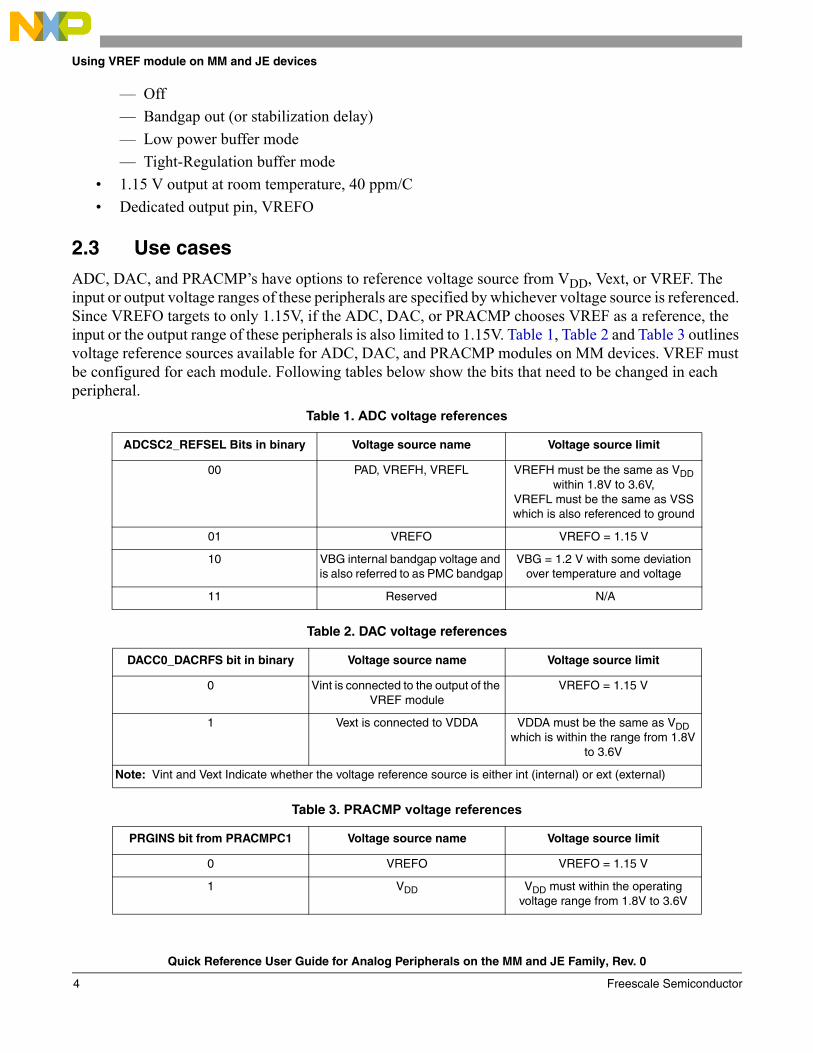
2.3 Use casesADC, DAC, and PRACMP’s have options to reference voltage source from VDD, Vext, or VREF. The input or output voltage ranges of these peripherals are specified by whichever voltage source is referenced. Since VREFO targets to only 1.15V, if the ADC, DAC, or PRACMP chooses VREF as a reference, the input or the output range of these peripherals is also limited to 1.15V. Table 1, Table 2 and Table 3 outlines voltage reference sources available for ADC, DAC, and PRACMP modules on MM devices. VREF must be configured for each module. Following tables below show the bits that need to be changed in each peripheral.
Table 1. ADC voltage references
ADCSC2_REFSEL Bits in binary Voltage source name Voltage source limit
00 PAD, VREFH, VREFL VREFH must be the same as VDD within 1.8V to 3.6V,
VREFL must be the same as VSS which is also referenced to ground
01 VREFO VREFO = 1.15 V
10 VBG internal bandgap voltage and is also referred to as PMC bandgap
VBG = 1.2 V with some deviation over temperature and voltage
11 Reserved N/A
Table 2. DAC voltage references
DACC0_DACRFS bit in binary Voltage source name Voltage source limit
0 Vint is connected to the output of the VREF module
VREFO = 1.15 V
1 Vext is connected to VDDA VDDA must be the same as VDD which is within the range from 1.8V
to 3.6V
Note: Vint and Vext Indicate whether the voltage reference source is either int (internal) or ext (external)
Table 3. PRACMP voltage references
PRGINS bit from PRACMPC1 Voltage source name Voltage source limit
0 VREFO VREFO = 1.15 V
1 VDD VDD must within the operating voltage range from 1.8V to 3.6V
Quick Reference User Guide for Analog Peripherals on the MM and JE Family, Rev. 0
Freescale Semiconductor4
Using VREF module on MM and JE devices
2.3.1 ADC using VREF
Table 1 above shows that when ADC selects VREF output as reference, ADC can only sample input voltage up to 1.15V. Although the sample voltage range is less than that of the other input voltage reference options, the advantage of using VREF as voltage reference is to allow ADC to sample with higher resolution.
Table 4 below shows that ADC sampling resolution can have three times the improvement if ADC voltage reference is VREF instead of VDD. One may intend to achieve the same resolution using VDD by supplying with 1.15V. However, this is not feasible because MM devices require VDD to be at least at 1.8V to operate. Using VREF as reference allows MCU VDD to stay within an operating voltage while providing the best sampling resolution with expected ADC input no larger than the 1.15V.
2.3.2 DAC using VREF
Similar to the case of ADC, for the dedicated 12-bit DAC where a higher output voltage resolution can be achieved if DAC selects VREF as a voltage source reference instead of the VDDA. The DAC output is up to 1.15V if VREF is the reference voltage and is up to 3.6V if VADDA is the reference voltage.
2.3.3 PRACMP using VREF
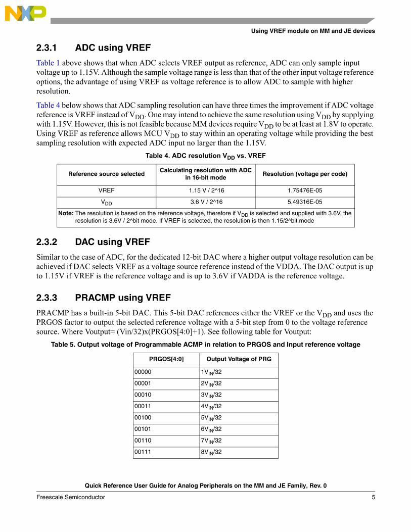
PRACMP has a built-in 5-bit DAC. This 5-bit DAC references either the VREF or the VDD and uses the PRGOS factor to output the selected reference voltage with a 5-bit step from 0 to the voltage reference source. Where Voutput= (Vin/32)x(PRGOS[4:0]+1). See following table for Voutput:
Table 4. ADC resolution VDD vs. VREF
Reference source selectedCalculating resolution with ADC
in 16-bit modeResolution (voltage per code)
VREF 1.15 V / 2^16 1.75476E-05
VDD 3.6 V / 2^16 5.49316E-05
Note: The resolution is based on the reference voltage, therefore if VDD is selected and supplied with 3.6V, the resolution is 3.6V / 2^bit mode. If VREF is selected, the resolution is then 1.15/2^bit mode
Table 5. Output voltage of Programmable ACMP in relation to PRGOS and Input reference voltage
PRGOS[4:0] Output Voltage of PRG
00000 1VIN/32
00001 2VIN/32
00010 3VIN/32
00011 4VIN/32
00100 5VIN/32
00101 6VIN/32
00110 7VIN/32
00111 8VIN/32
Quick Reference User Guide for Analog Peripherals on the MM and JE Family, Rev. 0
Freescale Semiconductor 5
Using VREF module on MM and JE devices
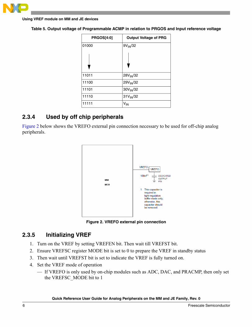
2.3.4 Used by off chip peripherals
Figure 2 below shows the VREFO external pin connection necessary to be used for off-chip analog peripherals.
Figure 2. VREFO external pin connection
2.3.5 Initializing VREF 1. Turn on the VREF by setting VREFEN bit. Then wait till VREFST bit.2. Ensure VREFSC register MODE bit is set to 0 to prepare the VREF in standby status3. Then wait until VREFST bit is set to indicate the VREF is fully turned on. 4. Set the VREF mode of operation
— If VREFO is only used by on-chip modules such as ADC, DAC, and PRACMP, then only set the VREFSC_MODE bit to 1
01000 9VIN/32
11011 28VIN/32
11100 29VIN/32
11101 30VIN/32
11110 31VIN/32
11111 VIN
Table 5. Output voltage of Programmable ACMP in relation to PRGOS and Input reference voltage
PRGOS[4:0] Output Voltage of PRG
Quick Reference User Guide for Analog Peripherals on the MM and JE Family, Rev. 0
Freescale Semiconductor6
Using VREF module on MM and JE devices
— If VREFO is intended to on-chip modules or off-chip (via the VREFO pin) or both, then set the VREFSC_MODE bit to 2. Please follow Figure 2 for VREFO external pin connection.
Below is the snippet C code setting VREF for used by both internal and external peripherals following above steps. VREFSC_VREFEN = 1; VREFSC_MODE = 0; while (!VREFSC_VREFST); VREFSC_MODE = 2;
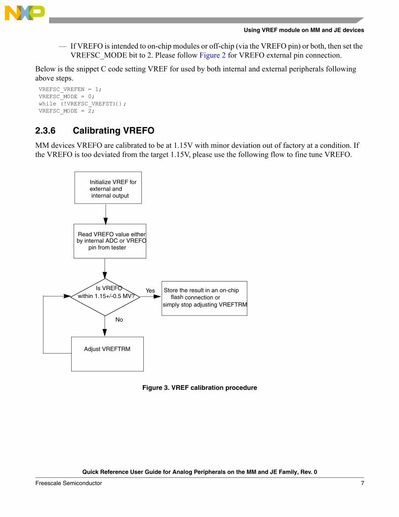
2.3.6 Calibrating VREFO
MM devices VREFO are calibrated to be at 1.15V with minor deviation out of factory at a condition. If the VREFO is too deviated from the target 1.15V, please use the following flow to fine tune VREFO.
Figure 3. VREF calibration procedure
Initialize VREF for external and internal output
Read VREFO value eitherby internal ADC or VREFO
pin from tester
Is VREFO within 1.15+/-0.5 MV?
Adjust VREFTRM
No
Store the result in an on-chip connection or flash
simply stop adjusting VREFTRM
Yes
Quick Reference User Guide for Analog Peripherals on the MM and JE Family, Rev. 0
Freescale Semiconductor 7
PDB module for MM and JE devices
3 PDB module for MM and JE devices
3.1 OverviewThe programmable delay module (PDB) is a key component in the medical measurement engine as it allows precise timing control over ADC conversions and DAC updates. Many applications would need to synchronize multiple ADC conversions with respect to an external triggering event and there is also requirement for changing sensor bias voltage during measurement. PDB module serves to provide the hardware trigger for ADC conversion and at the same time advance DAC buffer pointer (refer to Section 6.1, “Brief description) for signal conditioning.
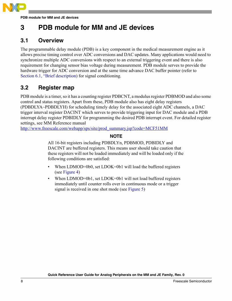
3.2 Register mapPDB module is a timer, so it has a counting register PDBCNT, a modulus register PDBMOD and also some control and status registers. Apart from these, PDB module also has eight delay registers (PDBDLYA~PDBDLYH) for scheduling timely delay for the associated eight ADC channels, a DAC trigger interval register DACINT which serves to provide triggering input for DAC module and a PDB interrupt delay register PDBIDLY for programming the desired PDB interrupt event. For detailed register settings, see MM Reference manual http://www.freescale.com/webapp/sps/site/prod_summary.jsp?code=MCF51MM
NOTEAll 16-bit registers including PDBDLYn, PDBMOD, PDBIDLY and DACINT are buffered registers. This means user should take caution that these registers will not be loaded immediately and will be loaded only if the following conditions are satisfied:
• When LDMOD=0b0, set LDOK=0b1 will load the buffered registers (see Figure 4)
• When LDMOD=0b1, set LDOK=0b1 will not load buffered registers immediately until counter rolls over in continuous mode or a trigger signal is received in one shot mode (see Figure 5)
Quick Reference User Guide for Analog Peripherals on the MM and JE Family, Rev. 0
Freescale Semiconductor8
PDB module for MM and JE devices
Figure 4. Register update with LDMOD=0b0
Figure 5. Registers update with LDMOD=0b1
Quick Reference User Guide for Analog Peripherals on the MM and JE Family, Rev. 0
Freescale Semiconductor 9
PDB module for MM and JE devices
3.3 Operation mode
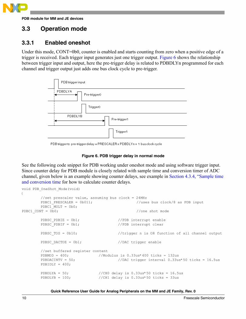
3.3.1 Enabled oneshot
Under this mode, CONT=0b0, counter is enabled and starts counting from zero when a positive edge of a trigger is received. Each trigger input generates just one trigger output. Figure 6 shows the relationship between trigger input and output, here the pre-trigger delay is related to PDBDLYn programmed for each channel and trigger output just adds one bus clock cycle to pre-trigger.
Figure 6. PDB trigger delay in normal mode
See the following code snippet for PDB working under oneshot mode and using software trigger input. Since counter delay for PDB module is closely related with sample time and conversion timer of ADC channel, given below is an example showing counter delays, see example in Section 4.3.4, “Sample time and conversion time for how to calculate counter delays.void PDB_OneShot_Mode(void)
//set prescaler value, assuming bus clock = 24MHzPDBC1_PRESCALER = 0b011; //uses bus clock/8 as PDB inputPDBC1_MULT = 0b0;
PDBC1_CONT = 0b0; //one shot mode
PDBSC_PDBIE = 0b1; //PDB interrupt enablePDBSC_PDBIF = 0b1; //PDB interrupt clear
PDBSC_TOS = 0b10; //trigger n is OR function of all channel output
PDBSC_DACTOE = 0b1; //DAC trigger enable
//set buffered register contentPDBMOD = 400; //Modulus is 0.33us*400 ticks = 132usPDBDACINTV = 50; //DAC trigger interval 0.33us*50 ticks = 16.5usPDBIDLY = 400;
PDBDLYA = 50; //CH0 delay is 0.33us*50 ticks = 16.5usPDBDLYB = 100; //CH1 delay is 0.33us*50 ticks = 33us
Quick Reference User Guide for Analog Peripherals on the MM and JE Family, Rev. 0
Freescale Semiconductor10
PDB module for MM and JE devices
PDBDLYC = 150; //CH2 delay is 0.33us*150 ticks = 49.5usPDBDLYD = 200; //CH3 delay is 0.33us*200 ticks = 66usPDBDLYE = 250; //CH4 delay is 0.33us*250 ticks = 82.5usPDBDLYF = 300; //CH5 delay is 0.33us*300 ticks = 99usPDBDLYG = 350; //CH6 delay is 0.33us*350 ticks = 115.5usPDBDLYH = 400; //CH7 delay is 0.33us*400 ticks = 132us
PDBSC_LDOK = 0b1; //load buffered registerswhile(PDBSC_LDOK); //wait till LDOK is cleared
PDBCHEN = 0xff; //enable all channel output
PDBSC_PDBEN = 0b1; //counter enable
void PDB_SoftwareTrig(void)PDBC1_TRIGSEL = 0b111; //software trigger input
PDBC2_SWTRIG = 0b1; //fire software trigger
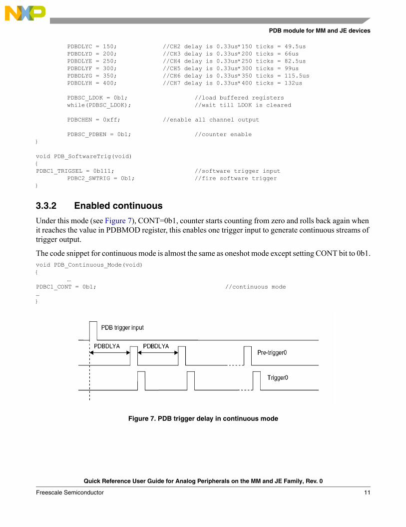
3.3.2 Enabled continuous
Under this mode (see Figure 7), CONT=0b1, counter starts counting from zero and rolls back again when it reaches the value in PDBMOD register, this enables one trigger input to generate continuous streams of trigger output.
The code snippet for continuous mode is almost the same as oneshot mode except setting CONT bit to 0b1.void PDB_Continuous_Mode(void)
…PDBC1_CONT = 0b1; //continuous mode…
Figure 7. PDB trigger delay in continuous mode
Quick Reference User Guide for Analog Peripherals on the MM and JE Family, Rev. 0
Freescale Semiconductor 11
PDB module for MM and JE devices
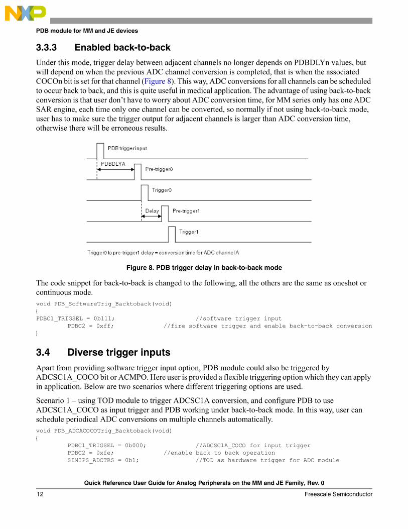
3.3.3 Enabled back-to-back
Under this mode, trigger delay between adjacent channels no longer depends on PDBDLYn values, but will depend on when the previous ADC channel conversion is completed, that is when the associated COCOn bit is set for that channel (Figure 8). This way, ADC conversions for all channels can be scheduled to occur back to back, and this is quite useful in medical application. The advantage of using back-to-back conversion is that user don’t have to worry about ADC conversion time, for MM series only has one ADC SAR engine, each time only one channel can be converted, so normally if not using back-to-back mode, user has to make sure the trigger output for adjacent channels is larger than ADC conversion time, otherwise there will be erroneous results.
Figure 8. PDB trigger delay in back-to-back mode
The code snippet for back-to-back is changed to the following, all the others are the same as oneshot or continuous mode.void PDB_SoftwareTrig_Backtoback(void)PDBC1_TRIGSEL = 0b111; //software trigger input
PDBC2 = 0xff; //fire software trigger and enable back-to-back conversion
3.4 Diverse trigger inputsApart from providing software trigger input option, PDB module could also be triggered by ADCSC1A_COCO bit or ACMPO. Here user is provided a flexible triggering option which they can apply in application. Below are two scenarios where different triggering options are used.
Scenario 1 – using TOD module to trigger ADCSC1A conversion, and configure PDB to use ADCSC1A_COCO as input trigger and PDB working under back-to-back mode. In this way, user can schedule periodical ADC conversions on multiple channels automatically.void PDB_ADCACOCOTrig_Backtoback(void)
PDBC1_TRIGSEL = 0b000; //ADCSC1A_COCO for input triggerPDBC2 = 0xfe; //enable back to back operationSIMIPS_ADCTRS = 0b1; //TOD as hardware trigger for ADC module
Quick Reference User Guide for Analog Peripherals on the MM and JE Family, Rev. 0
Freescale Semiconductor12
PDB module for MM and JE devices
//configure TOD for periodical ADC conversion, trigger for every 0.25s TODC_TODR = 0b1; //TOD counter resetTODC_TODCLKS = 0b00; //OSCOUT as TOD clock inputTODC_TODPS = 0b001; //for 32.768kHz
TODSC_QSECF = 0b1; //quarter second flag clearTODSC_QSECIE = 0b1; //quarter second interrupt enable
TODC_TODEN = 0b1; //TOD enable
Scenario 2 – using ACMPO as input trigger for PDB module, this provides a way for triggering ADC conversions under certain conditions, for example, input biosensor value is greater than some threshold. void PDB_ACMPOTrig(void)
PDBC1_TRIGSEL = 0b001; //ACMPO for input trigger
PRACMPC1_PRGINS = 0b1; //PRG select external power as referencePRACMPC1_PRGOS = 0b00101; //PRG out = 6/32*VinPRACMPC1_PRGEN = 0b1; //PRG enablePRACMPC0_ACPSEL = 0b100; //ACMP positive input is OPAMP out0PRACMPC0_ACNSEL = 0b111; //ACMP negative input is internal PRG
output
PRACMPCS_ACEN = 0b1; //ACMP enable
3.5 Relationship between PDB, ADC and DAC moduleADC module will initiate an ADC conversion if the hardware trigger source ADHWT is enabled and the associated hardware trigger event ADHWTSn has occurred, here ADHWTSn is related to the eight channels for hardware trigger in ADC module. Table 6 illustrates the connection between PDB pre-trigger, trigger outputs with the above trigger source and events.
Now getting back to the enabled oneshot example, where the PDB is needed to trigger successive ADC conversions on channel A to H selected by ADCSC1n, here TOS will be configured to be OR function of
Table 6. PDB trigger and pre-trigger connection to ADC module
PDB Trigger or pre-trigger ADC trigger or event Associated ADC register
Trigger0 ADHWT Triggers ADC conversion
Pre-trigger0 ADHWTSA Selects ADCSC1A
Pre-trigger1 ADHWTSB Selects ADCSC1B
Pre-trigger2 ADHWTSC Selects ADCSC1C
Pre-trigger3 ADHWTSD Selects ADCSC1D
Pre-trigger4 ADHWTSE Selects ADCSC1E
Pre-trigger5 ADHWTSF Selects ADCSC1F
Pre-trigger6 ADHWTSG Selects ADCSC1G
Pre-trigger7 ADHWTSH Selects ADCSC1H
Quick Reference User Guide for Analog Peripherals on the MM and JE Family, Rev. 0
Freescale Semiconductor 13

ADC module for MM devices
all channel outputs, see Figure 9 for an illustration of why OR function is needed. Please note only PDB trigger0 output can trigger ADC conversions, while the eight pre-triggers from PDB module are used to select respective ADC channels configured by ADCSC1n.
Figure 9. Illustration of TOS OR function
PDB trigger connection to DAC module is much simpler, when DAC is not in buffered mode, each DAC trigger will result a DAC conversion on DACDAT0; for DAC buffered mode, each trigger will result a conversion on current DAC word and advance the data pointer to next word in DAC buffer.
4 ADC module for MM devices
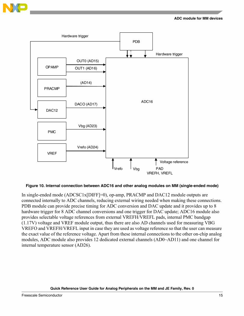
4.1 OverviewThis is a quick reference for using the 16-bit successive approximation ADC module integrated on MM family. The ADC module is part of the measurement engine of MM family, it supports 4 pairs of differential and 24 single-ended analog inputs and has internal connection with other analog modules integrated on MM depending on which mode it’s operating. Figure 10 shows the case when ADC module works under single-ended mode, while Figure 11 shows the case for differential mode.
PDB trigger input
Pre-trigger0
Trigger0
PDBDLYA
PDBDLYB
Trigger1
PDBDLYC
Pre-trigger1
Pre-trigger2
Trigger2
Pre-trigger7
Trigger7
PDBDLYH
Quick Reference User Guide for Analog Peripherals on the MM and JE Family, Rev. 0
Freescale Semiconductor14
ADC module for MM devices
Figure 10. Internal connection between ADC16 and other analog modules on MM (single-ended mode)
In single-ended mode (ADCSC1x[DIFF]=0), op-amp, PRACMP and DAC12 module outputs are connected internally to ADC channels, reducing external wiring needed when making these connections. PDB module can provide precise timing for ADC conversion and DAC update and it provides up to 8 hardware trigger for 8 ADC channel conversions and one trigger for DAC update; ADC16 module also provides selectable voltage references from external VREFH/VREFL pads, internal PMC bandgap (1.17V) voltage and VREF module output, thus there are also AD channels used for measuring VBG VREFO and VREFH/VREFL input in case they are used as voltage reference so that the user can measure the exact value of the reference voltage. Apart from these internal connections to the other on-chip analog modules, ADC module also provides 12 dedicated external channels (AD0~AD11) and one channel for internal temperature sensor (AD26).
ADC16
OPAMP
OUT0 (AD15)
OUT1 (AD16)
PRACMP
DAC12
DACO (AD17)
PMC
Vbg (AD23)
PDB
PAD VREFH, VREFL
Vbg Vrefo
Hardware trigger
Voltage reference
(AD14)
Hardware trigger
VREF
Vrefo (AD24)
Quick Reference User Guide for Analog Peripherals on the MM and JE Family, Rev. 0
Freescale Semiconductor 15
ADC module for MM devices
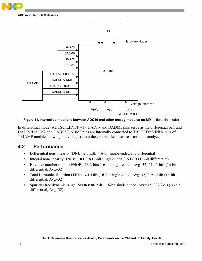
Figure 11. Internal connections between ADC16 and other analog modules on MM (differential mode)
In differential mode (ADCSC1x[DIFF]=1), DADPx and DADMx pins serve as the differential pair and DADP2/DADM2 and DADP3/DADM3 pins are internally connected to TRIOUTx/ VINNx pins of TRIAMP module allowing the voltage across the external feedback resistor to be analyzed.
4.2 Performance• Differential non-linearity (DNL): 2.5 LSB (16-bit single-ended and differential)• Integral non-linearity (INL): ±10 LSB(16-bit single-ended)/±6 LSB (16-bit differential)• Effective number of bits (ENOB): 13.2-bits (16-bit single ended, Avg=32) / 14.2-bits (16-bit
differential, Avg=32)• Total harmonic distortion (THD): -85.5 dB (16-bit single ended, Avg=32) / -91.5 dB (16-bit
differential, Avg=32)• Spurious free dynamic range (SFDR): 86.2 dB (16-bit single ended, Avg=32) / 92.2 dB (16-bit
differential, Avg=32)
ADC16
PAD VREFH, VREFL
Vbg Vrefo
Voltage reference
PDB
Hardware trigger
DADP0
DADM0
DADP1
DADM1
DADP2/TRIPUT0
DADM2/VINN0
DADP3/TRIOUT1
DADM3/VINN1
TRIAMP
Quick Reference User Guide for Analog Peripherals on the MM and JE Family, Rev. 0
Freescale Semiconductor16
ADC module for MM devices
4.3 Main characteristicsFeatures of ADC module include:
• Up to 4 pairs of differential and 24 single-ended external analog inputs• Output Modes:
— Differential 16-bit, 13-bit, 11-bit, and 9-bit modes— Single-ended 16-bit, 12-bit, 10-bit, and 8-bit modes
• Single or continuous conversion (automatic return to idle after single conversion)• Configurable sample time and conversion speed/power• Input clock selectable from up to four sources• Operation in wait or stop3 modes for lower noise operation• Asynchronous clock source for lower noise operation with option to output the clock• Selectable asynchronous hardware conversion trigger with hardware channel select• Automatic compare with interrupt for less-than, greater-than or equal-to, within range, or
out-of-range, programmable value• Hardware average function• Selectable voltage reference• Self-Calibration mode
4.3.1 Conversion trigger options
ADC16 module can be configured as software or hardware trigger based on ADCSC2[ADTRG] bit. When ADTRG=0, the module is configured as software trigger mode and following a write to ADCSC1A with ADCHA bits not all 1’s, ADC module will initiate a conversion on the associated channel. When ADTRG=1, then if the ADHWT source is available, a conversion is initiated on the rising edge of the ADHWT after a hardware trigger select event (ADHWTSn) has occurred. Here the ADHWT trigger source comes from TOD (Time of Day) or PDB (Programmable Delay Block) module depending on ADCTRS bit in SIMIPS register. Table 7 is a summary for ADC trigger option and associated register configuration on MM device.
There are eight hardware trigger sources from PDB module (refer to Section 3.5, “Relationship between PDB, ADC and DAC module) on MM device. End user can program values to PDBDLYn register to arrange ADC conversions in a timely manner other than making sure time between adjacent trigger should be longer than one ADC conversion, as there is only one SAR engine in ADC module, two ADC channel conversions cannot be performed at the same time. In the same way, ADC module also has eight
Table 7. Trigger option and register configuration for ADC module
Software trigger ADCSC2[ADTRG]=0 && ADCSC1A[ADCHA] = channel number (other than all 1’s)
TOD trigger ADCSC2[ADTRG]=1 && SIMIPS[ADCTRS]=1 && TOD interrupt occurred
PDB trigger ADCSC2[ADTRG]=1 && SIMIPS[ADCTRS]=0 && PDB trigger source available
Quick Reference User Guide for Analog Peripherals on the MM and JE Family, Rev. 0
Freescale Semiconductor 17
ADC module for MM devices
ADCSC1n registers to support hardware trigger up to eight channels, here ADCSC1A is used for both software and hardware trigger modes of operation, while ADCSC1B~ADCSC1H are used only for hardware trigger mode.
In the same way, ADC module also has eight ADCSC1n registers to support hardware trigger up to eight channels, here ADCSC1A is used for both software and hardware trigger modes of operation, while ADCSC1B~ADCSC1H are used only for hardware trigger mode.
When working under hardware trigger mode, each channel control register ADCSC1n is configured to select which channel to convert by setting ADCHn bits and whether to use single-ended mode or differential mode for conversion by setting DIFF bit. User can program the associated PDBDLYn register to schedule desired trigger delay, this will enable user precise control of time when each ADC channel trigger is fired. When ADC conversion is completed, the COCO bit in corresponding ADCSC1n register is set and AIENn bit can be set to generate the conversion complete interrupt, then user can read the conversion result in the interrupt service routine with associated ADCRn register. See Table 8 for register relationship between ADC and PDB module under hardware trigger mode.
Since each ADCSC1n register has its own DIFF bit, user is given much flexibility to configure some channels to work as single-ended mode, while others as differential mode and use PDB module to trigger their conversion sequentially.
4.3.2 Automatic compare
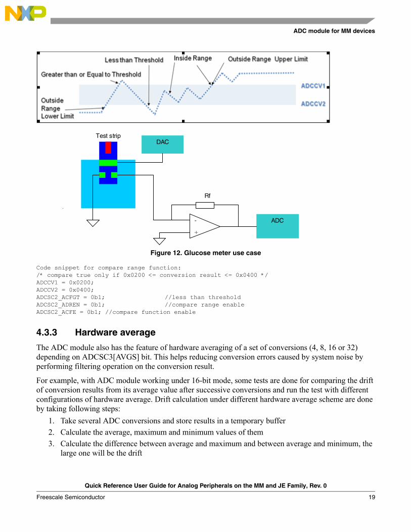
The ADC16 module has support for automatic compare so end user can configure the module to check if the result is less than or greater-than-or-equal-to a single compare value, or if the result falls within or outside a range determined by two compare values. The compare mode is determined by ACFGT, ACREN and the values in the compare value registers (ADCCV1 and ADCCV2). When ACREN=0, then only ADCCV1 is used for single comparison where ACFGT determines less than or greater than the threshold; when ACREN=1, then both ADCCV1 and ADCCV2 are used for compare range function. The added compare range function helps reducing a complex comparator circuit in application where it’s necessary, for instance like the use case in glucose meter application (Figure 12). Here DAC module provides the bias voltage across test strip to begin the chemical reaction; the output of test strip will be a current and is converted to voltage with trans-impedance amplifier; the output of trans-impedance amplifier is monitored for a proper sample so that it can be within some range.
Table 8. Register relationship between ADC and PDB module in hardware trigger mode
Channel configuration Programmable trigger delay Conversion result
ADCSC1A PDBDLYA ADCRA
ADCSC1B PDBDLYB ADCRB
ADCSC1C PDBDLYC ADCRC
ADCSC1D PDBDLYD ADCRD
ADCSC1E PDBDLYE ADCRE
ADCSC1F PDBDLYF ADCRF
ADCSC1G PDBDLYG ADCRG
ADCSC1H PDBDLYH ADCRH
Quick Reference User Guide for Analog Peripherals on the MM and JE Family, Rev. 0
Freescale Semiconductor18
ADC module for MM devices
Figure 12. Glucose meter use case
Code snippet for compare range function:/* compare true only if 0x0200 <= conversion result <= 0x0400 */ADCCV1 = 0x0200;ADCCV2 = 0x0400;ADCSC2_ACFGT = 0b1; //less than thresholdADCSC2_ADREN = 0b1; //compare range enableADCSC2_ACFE = 0b1; //compare function enable
4.3.3 Hardware average
The ADC module also has the feature of hardware averaging of a set of conversions (4, 8, 16 or 32) depending on ADCSC3[AVGS] bit. This helps reducing conversion errors caused by system noise by performing filtering operation on the conversion result.
For example, with ADC module working under 16-bit mode, some tests are done for comparing the drift of conversion results from its average value after successive conversions and run the test with different configurations of hardware average. Drift calculation under different hardware average scheme are done by taking following steps:
1. Take several ADC conversions and store results in a temporary buffer 2. Calculate the average, maximum and minimum values of them3. Calculate the difference between average and maximum and between average and minimum, the
large one will be the drift
-
+
ADC
DAC Test strip
Rf
Quick Reference User Guide for Analog Peripherals on the MM and JE Family, Rev. 0
Freescale Semiconductor 19
ADC module for MM devices
Following is the code snippet for drift calculation:for(i = 0; i < BUFFER_SIZE; i++) total += result[i]; if(maximum < result[i]) maximum = result[i]; if(minimum > result[i]) minimum = result[i]; average = total/BUFFER_SIZE; if((maximum - average)>(average - minimum)) driff = maximum - average; else driff = average - minimum;
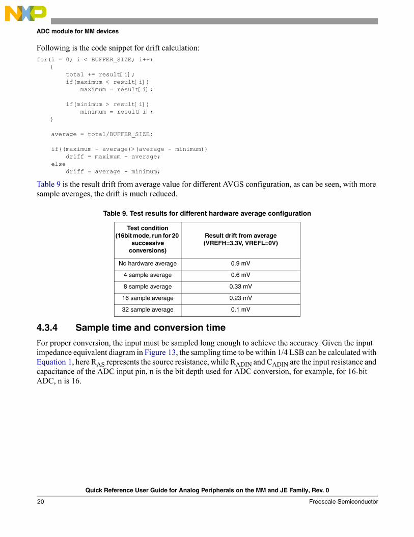
Table 9 is the result drift from average value for different AVGS configuration, as can be seen, with more sample averages, the drift is much reduced.
4.3.4 Sample time and conversion time
For proper conversion, the input must be sampled long enough to achieve the accuracy. Given the input impedance equivalent diagram in Figure 13, the sampling time to be within 1/4 LSB can be calculated with Equation 1, here RAS represents the source resistance, while RADIN and CADIN are the input resistance and capacitance of the ADC input pin, n is the bit depth used for ADC conversion, for example, for 16-bit ADC, n is 16.
Table 9. Test results for different hardware average configuration
Test condition(16bit mode, run for 20
successive conversions)
Result drift from average(VREFH=3.3V, VREFL=0V)
No hardware average 0.9 mV
4 sample average 0.6 mV
8 sample average 0.33 mV
16 sample average 0.23 mV
32 sample average 0.1 mV
Quick Reference User Guide for Analog Peripherals on the MM and JE Family, Rev. 0
Freescale Semiconductor20

ADC module for MM devices
Figure 13. ADC input impedance equivalent diagram
Eqn. 1
The conversion time can be calculated with Equation 2 and the meaning of each component is explained in Table 10. Here the ADC conversion time also includes sampling time, so user has to make sure the SFCAdder component is greater than tsample.
Eqn. 2
Table 10. Conversion time component explanation
Component Meaning
SFCAdder Single or first continuous time adder, depends on the clock source chosen
(ADICLK), whether using long sample time or not (ADLSMP)
AverageNum Average number factor, could be 1, 4, 8, 16 or 32
BCT Base conversion time, depends on ADC conversion mode MODE, DIFFn
LSTAdder Long sample time adder, allows high impedance inputs to accurately sampled
(ADLSMP and ADLSTS)
HSTAdder Used when ADCLK exceeds the limit for ADHSC=0
( ) ( )( )2n2^lnCRRt ADINASADINsample +××+=
( )HSTAdderLSTAdderBCTAverageNumSFCAddertconversion ++×+=
Quick Reference User Guide for Analog Peripherals on the MM and JE Family, Rev. 0
Freescale Semiconductor 21
ADC module for MM devices
Following is an example of how to calculate ADC conversion time based on a specific register setting. 1. Assume bus clock is 24 MHz, if user configures ADC module to work under 16bit mode and
ADLPC=0b0, ADHSC=0b0 for normal operation, then the ADC input clock should be between 1 MHz and 5 MHz (see MM series datasheet, find in the Table 15 16-bit SAR ADC operating conditions and Row 10 for ADC conversion clocks http://www.freescale.com/webapp/sps/site/prod_summary.jsp?code=MCF51MM).ADCCFG1_ADLPC = 0; //normal powerADCCFG2_ADHSC = 0; //normal conversionADCCFG1_MODE = 0b11; //16-bit mode
2. Configure ADC input clock with following setting so that it’s 3 MHz//fADACK = fbus/8 = 3 MHz, assuming 24MHz bus clockADCCFG1_ADICLK = 0b00; //bus clockADCCFG1_ADIV = 0b11; //div by 8
3. Calculate needed minimum sample time for given input resistance (Radin), analog source resistance (Ras) and input capacitance (Cadin). For example, if Radin = 7 kΩ, Ras = 2 kΩ, Cadin = 10 pF for 16-bit mode, then with Equation 1, sample time should be at least 4 ADACK cycle for fADCK = 3 MHz.ADCCFG1_ADLSMP = 1; //long sample timeADCCFG2_ADLSTS = 0b11; //2 extra ADACK cycles
4. Calculate total conversion time with equation 2, so conversion time in this case is about 10.1us
NOTEFor hardware triggering with PDB module, the channel delay between adjacent ADC channels must be greater than ADC conversion time of the previous channel. That is why in the code snippet in PDB module, the PDB interval is set to be 16.5µs which is large enough for the conversion time in the above setting. But for PDB back to back operation, for next channel ADC trigger will not be fired until previous channel conversion is completed.
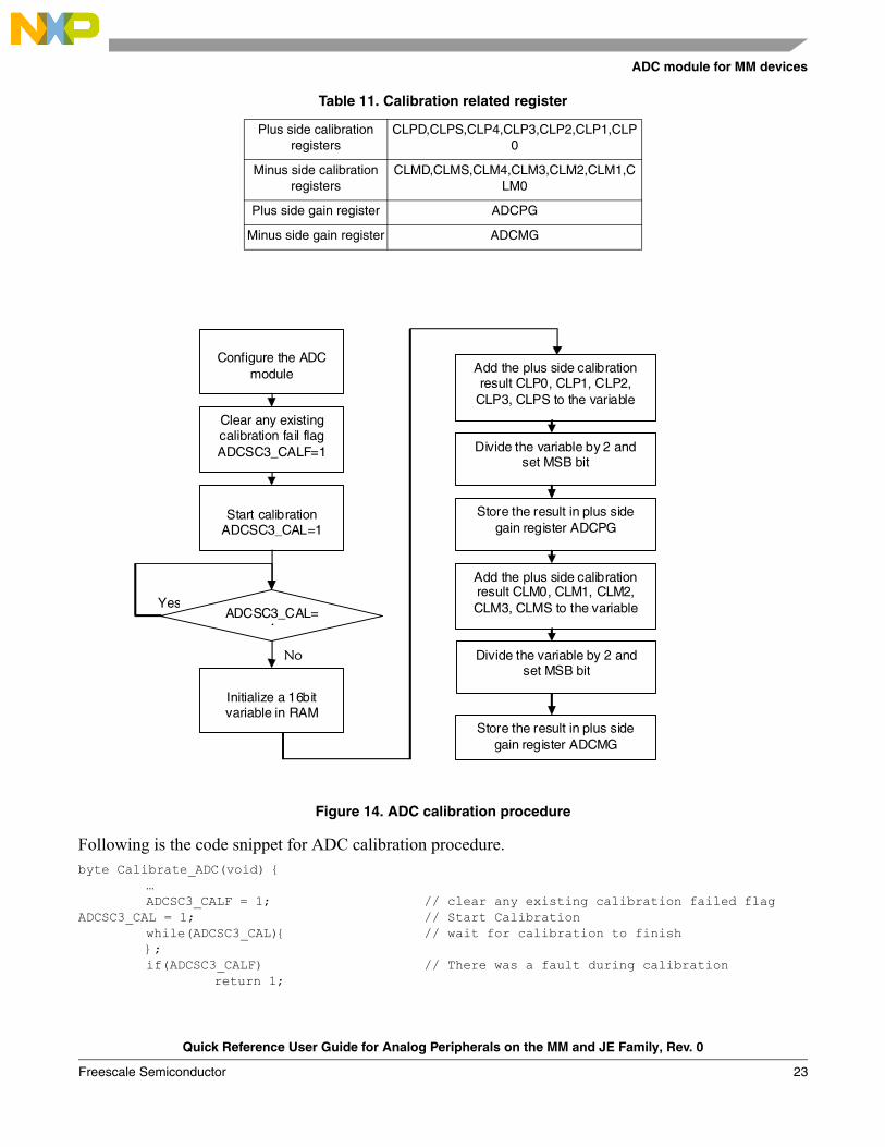
4.4 Calibration procedureThe ADC module contains a self-calibration function which needs to be run after any reset and before a conversion is initiated. The calibration function sets the offset calibration value and plus side and minus side calibration values. User must configure ADC module before calibration and configure the plus side and minus side gain registers after calibration is completed. Table 11 lists the registers related to calibration function. The ADC calibration procedure is shown in Table 11.
Table 11. Calibration related register
Component Meaning
Offset registers ADCOFS
Quick Reference User Guide for Analog Peripherals on the MM and JE Family, Rev. 0
Freescale Semiconductor22
ADC module for MM devices
Figure 14. ADC calibration procedure
Following is the code snippet for ADC calibration procedure.byte Calibrate_ADC(void)
…ADCSC3_CALF = 1; // clear any existing calibration failed flag
ADCSC3_CAL = 1; // Start Calibrationwhile(ADCSC3_CAL) // wait for calibration to finish;if(ADCSC3_CALF) // There was a fault during calibration
return 1;
Plus side calibration registers
CLPD,CLPS,CLP4,CLP3,CLP2,CLP1,CLP0
Minus side calibration registers
CLMD,CLMS,CLM4,CLM3,CLM2,CLM1,CLM0
Plus side gain register ADCPG
Minus side gain register ADCMG
Table 11. Calibration related register
Configure the ADC module
Start calibration
ADCSC3_CAL=1
ADCSC3_CAL=1
Initialize a 16bit variable in RAM
Add the plus side calibration result CLP0, CLP1, CLP2,
CLP3, CLPS to the variable
Clear any existing calibration fail flag ADCSC3_CALF=1 Divide the variable by 2 and
set MSB bit
Store the result in plus side gain register ADCPG
Add the plus side calibration result CLM0, CLM1, CLM2, CLM3, CLMS to the variable
Divide the variable by 2 and set MSB bit
Store the result in plus side gain register ADCMG
No
Yes
Quick Reference User Guide for Analog Peripherals on the MM and JE Family, Rev. 0
Freescale Semiconductor 23
ADC module for MM devices
// Initialize (clear) a 16b variable in RAM.cal_temp = 0;
//Add the following plus-side calibration results CLP0, CLP1, CLP2, CLP3, CLP4, CLPS and CLPD to the variable.
cal_temp += ADCCLP0;cal_temp += ADCCLP1;cal_temp += ADCCLP2;cal_temp += ADCCLP3;cal_temp += ADCCLP4;
cal_temp += ADCCLPS;cal_temp += ADCCLPD;
// Divide the variable by two.cal_temp = cal_temp >> 1;
// Set the MSB of the variable.cal_temp |= 0x8000;
// Store the value in the plus-side gain calibration registers ADCPGADCPG = cal_temp;
// Repeat the procedure for the minus-side gain calibration value.
// Initialize (clear) a 16b variable in RAM.cal_temp = 0;
//Add the following minus-side calibration results CLM0, CLM1, CLM2, CLM3, CLM4, CLMS and CLMD to the variable.
cal_temp += ADCCLM0;cal_temp += ADCCLM1;cal_temp += ADCCLM2;cal_temp += ADCCLM3;cal_temp += ADCCLM4;cal_temp += ADCCLMS;cal_temp += ADCCLMD;
// Divide the variable by two.cal_temp = cal_temp >> 1;
// Set the MSB of the variable.cal_temp |= 0x8000;
// Store the value in the minus-side gain calibration registers ADCMGADCMG = cal_temp;
// Clear the CAL bitADCCFG3_CAL = 0;
return 0;
Quick Reference User Guide for Analog Peripherals on the MM and JE Family, Rev. 0
Freescale Semiconductor24
ADC module for MM devices
4.5 Filter stageMedical signals coming from biosensor contain undesired frequency elements, so its necessary to implement appropriate filter stage especially low pass filters to remove those elements before they are sampled and converted by ADC module.
A number of literature is available describing how to design active filters with op-amp and the method is so systematic that user can first decide the filter characteristics such as corner frequency, filter type and topology and then calculate the passive components of the filter with the help of a filter table.
Filter type is determined by one of the following three factors of gain and phase response of the filter: passband flatness, passband to stopband transition and linear phase response. According to this, three types of filters (Butterworth, Tschebyscheff and Bessel) with predetermined coefficients have been listed out in table form for easy calculation.
The general transfer function of a low pass filter is in Equation 3.
Eqn. 3
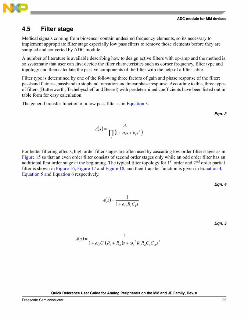
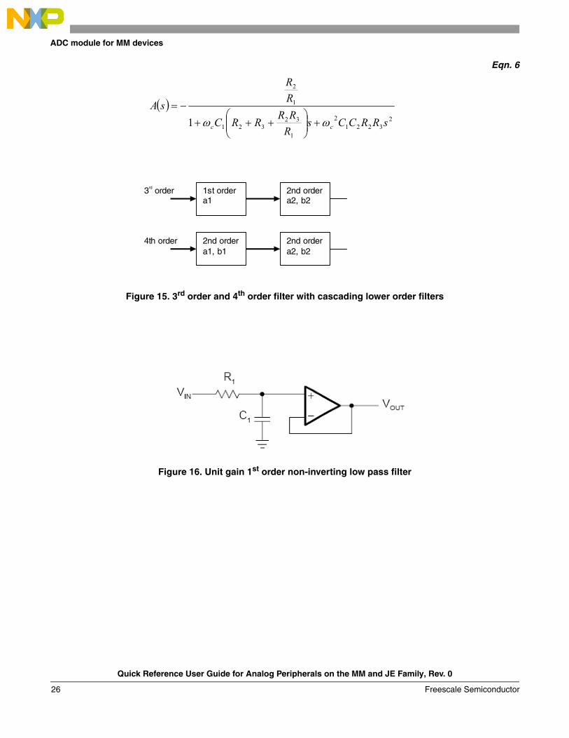
For better filtering effects, high order filter stages are often used by cascading low order filter stages as in Figure 15 so that an even order filter consists of second order stages only while an odd order filter has an additional first order stage at the beginning. The typical filter topology for 1st order and 2nd order partial filter is shown in Figure 16, Figure 17 and Figure 18, and their transfer function is given in Equation 4, Equation 5 and Equation 6 respectively.
Eqn. 4
Eqn. 5
( ) ( )∏ ++=
iii sbsa
AsA 2
0
1
( )sCR
sAc 1111
ω+=
( )( ) 2
21212
21111
sCCRRsRRCsA
cc ωω +++=
Quick Reference User Guide for Analog Peripherals on the MM and JE Family, Rev. 0
Freescale Semiconductor 25
ADC module for MM devices
Eqn. 6
Figure 15. 3rd order and 4th order filter with cascading lower order filters
Figure 16. Unit gain 1st order non-inverting low pass filter
( )2
32212
1
32321
1
2
1 sRRCCsRRR
RRC
RR
sA
cc ωω +⎟⎟⎠
⎞⎜⎜⎝
⎛+++
−=
1st ordera1
2nd ordera2, b2
2nd ordera1, b1
2nd ordera2, b2
3rd order
4th order
Quick Reference User Guide for Analog Peripherals on the MM and JE Family, Rev. 0
Freescale Semiconductor26

ADC module for MM devices
Figure 17. Unit gain Sallen-Key 2nd order low pass filter
Figure 18. 2nd order MFB low pass filter
So for designing a high order low pass filter, the following steps can be followed based on the desired filter characteristics.
1. Determine the filter type to use, normally for maximum passband flatness, a Butterworth filter will be chosen
2. Decide filter stage, high filter stage helps sharpen passband to stopband transition but it also needs more hardware
3. Decide which topology to use, in most cases Sallen-key is sufficient, but if higher Q and gain is desired, MFB topology can be used instead
4. Set the desired corner frequency fc and passband gain A05. Work on each partial filter, compare the partial coefficient in filter table (determined by filter type,
see the Butterworth filter table in Table 12) with the associated coefficient in transfer function (determined by filter topology), then calculate the value of passive component based on desired corner frequency
Quick Reference User Guide for Analog Peripherals on the MM and JE Family, Rev. 0
Freescale Semiconductor 27
ADC module for MM devices
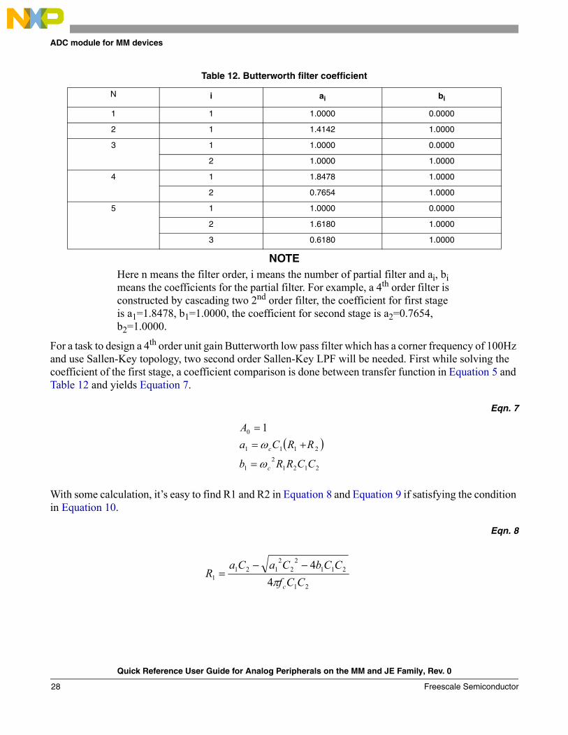
NOTEHere n means the filter order, i means the number of partial filter and ai, bi means the coefficients for the partial filter. For example, a 4th order filter is constructed by cascading two 2nd order filter, the coefficient for first stage is a1=1.8478, b1=1.0000, the coefficient for second stage is a2=0.7654, b2=1.0000.
For a task to design a 4th order unit gain Butterworth low pass filter which has a corner frequency of 100Hz and use Sallen-Key topology, two second order Sallen-Key LPF will be needed. First while solving the coefficient of the first stage, a coefficient comparison is done between transfer function in Equation 5 and Table 12 and yields Equation 7.
Eqn. 7
With some calculation, it’s easy to find R1 and R2 in Equation 8 and Equation 9 if satisfying the condition in Equation 10.
Eqn. 8
Table 12. Butterworth filter coefficient
N i ai bi
1 1 1.0000 0.0000
2 1 1.4142 1.0000
3 1 1.0000 0.0000
2 1.0000 1.0000
4 1 1.8478 1.0000
2 0.7654 1.0000
5 1 1.0000 0.0000
2 1.6180 1.0000
3 0.6180 1.0000
( )2121
21
2111
0 1
CCRRb
RRCaA
c
c
ω
ω
=
+==
21
2112
22
1211 4
4CCf
CCbCaCaR
cπ−−
=
Quick Reference User Guide for Analog Peripherals on the MM and JE Family, Rev. 0
Freescale Semiconductor28

Op-amp Module for MM devices
Eqn. 9
Eqn. 10
Specifying C1=22 nF, with Equation 10, C2=25.77 nF, so we choose C2=47 nF. Inserting a1 and b1 into Equation 9 and Equation 10 results in R1=22kΩ and R2=112 kΩ.
For the second stage, the same calculation is done except replacing a1, b1 with a2=0.7654 and b2=1.0000. Specifying C1=5.6 nF, C2=47 nF, R1=62 kΩ, R2= 156 kΩ is achieved.
4.6 ADC power consumption The ADC module can still work under wait mode or stop3 mode with ADACK chosen as its conversion clock if it’s configured to operate in continuous mode or using hardware trigger. Power consumption for each mode is list in Table 13.
5 Op-amp Module for MM devices
5.1 Op-amp Basic definitions The operational amplifier (op-amp) is one of the most important components of analog electronics. An op-amp is in essence a differential amplifier, which consist of two inputs, and one output. The output is proportional to the difference between the two inputs.
The operational amplifier symbol shown in Figure 19 is almost a black box for developers, who don’t care what is inside, but how the device will behave under certain configurations.
Table 13. ADC power consumption
Current on VDDA
Operation mode (16-bit, ADCO=1, ADACK as ADC input clock)
ADLSMP = 0 ADLSMP=1
ADLPC=0, ADHSC=0 597 µA 354 µA
ADLPC=1, ADHSC=0 227.4 µA 140 µA
ADLPC=0, ADHSC=1 778 µA 486 µA
21
2112
22
1212 4
4CCf
CCbCaCaR
cπ−+
=
21
112
4ab
CC ≥
Quick Reference User Guide for Analog Peripherals on the MM and JE Family, Rev. 0
Freescale Semiconductor 29

Op-amp Module for MM devices
Figure 19. Operational Amplifier Symbol
5.1.1 Ideal Op-amp golden rules 1. The voltage difference between inputs V+ and V– is zero
V2 – V1 = 02. The inputs draw no current
I1 = 0 I2 = 0
It is not a surprise that the ideal Golden Rules are not exact. Here are some departures from ideal performance
5.1.2 Offset voltage (VOS)
Recall that the input of the op-amp is a differential pair. If the two internal transistors are not perfectly matched, an offset will show up as non-zero DC offset at the output.
The offset voltage (VOS) equals to the differential input voltage that must be applied to an operation amplifier in order to obtain a zero frequency output voltage at zero volts.
The output offset voltage is defined as the measured output voltage when the input terminals are shorted together Figure 20.
Figure 20. Offset voltage
5.1.3 Bias current (Ibias)
Most developers forget that operational amplifiers are actually made with transistors. In practice the op-amp transistor inputs do draw some current, regardless of golden rule 2(see Section 5.1.1, “Ideal Op-amp golden rules.
Op-amps with bipolar transistor input drain more current through their inputs pins, than FET or MOSFET transistors. The bias current (Ibias) is defined to be the average of the currents of the two inputs.
+
–I1
I2
V1
V2
Quick Reference User Guide for Analog Peripherals on the MM and JE Family, Rev. 0
Freescale Semiconductor30
Op-amp Module for MM devices
Figure 21. Input bias Current
5.1.4 Offset current (Ios)
This is the difference between the input bias currents. Each bias current, after passing through an input resistive network, will effectively over a voltage to the op-amp input. Therefore, an offset of the two currents will show up as a voltage offset at the output.
5.1.5 Common-mode rejection ratio (CMRR)
If the two inputs of a differential amplifier were to be shorted together, there should be no change in the output voltage for any amount of voltage applied between those two shorted inputs and ground as shown in Figure 22.
Figure 22. Common-mode Voltage
The performance of a real op-amp is most commonly measured in terms of its differential voltage gain versus its common-mode voltage gain. This ratio is also called common-mode rejection ratio, abbreviated as CMRR:
+
–I+
I-
+
–
VIN
VO
Quick Reference User Guide for Analog Peripherals on the MM and JE Family, Rev. 0
Freescale Semiconductor 31
Op-amp Module for MM devices
5.1.6 Single supply Op-amp
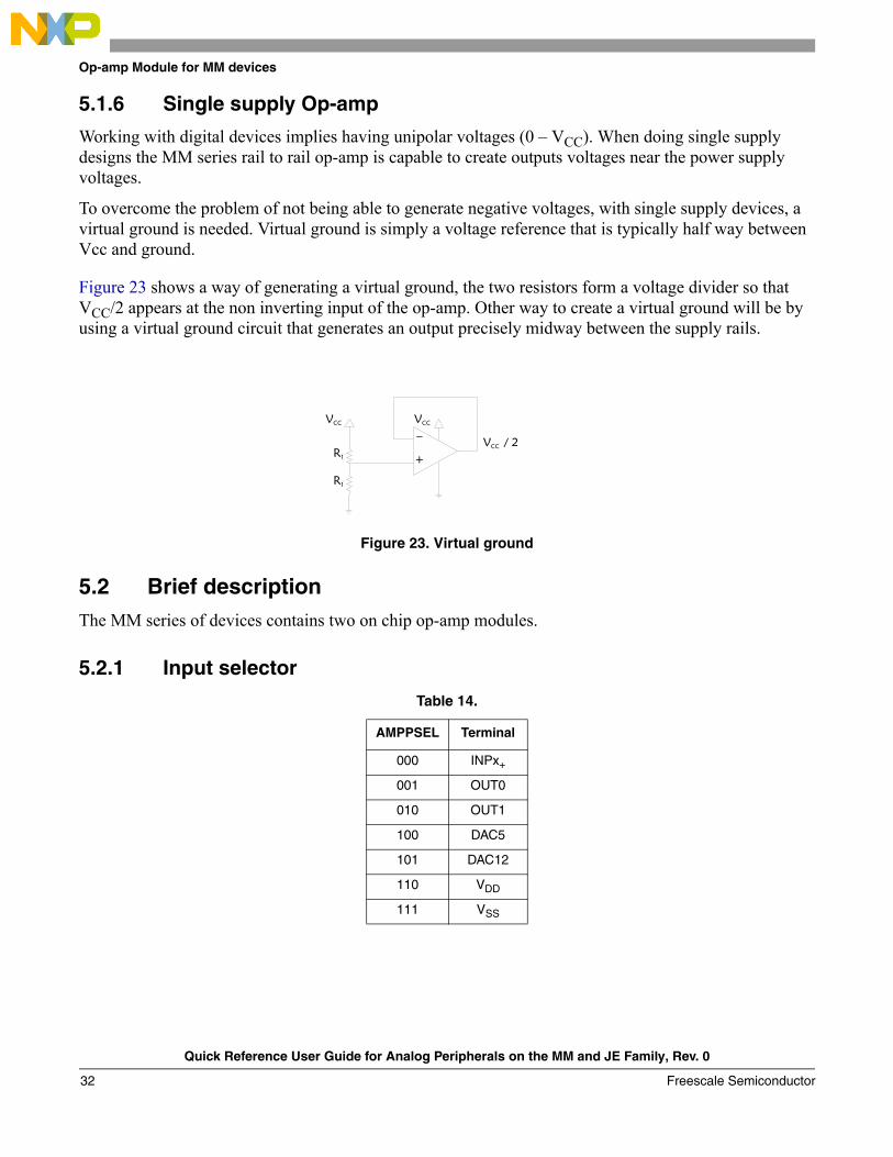
Working with digital devices implies having unipolar voltages (0 – VCC). When doing single supply designs the MM series rail to rail op-amp is capable to create outputs voltages near the power supply voltages.
To overcome the problem of not being able to generate negative voltages, with single supply devices, a virtual ground is needed. Virtual ground is simply a voltage reference that is typically half way between Vcc and ground.
Figure 23 shows a way of generating a virtual ground, the two resistors form a voltage divider so that VCC/2 appears at the non inverting input of the op-amp. Other way to create a virtual ground will be by using a virtual ground circuit that generates an output precisely midway between the supply rails.
Figure 23. Virtual ground
5.2 Brief descriptionThe MM series of devices contains two on chip op-amp modules.
5.2.1 Input selector
Table 14.
AMPPSEL Terminal
000 INPx+
001 OUT0
010 OUT1
100 DAC5
101 DAC12
110 VDD
111 VSS
+
– VCC / 2
VCC
R1
VCC
R1
Quick Reference User Guide for Analog Peripherals on the MM and JE Family, Rev. 0
Freescale Semiconductor32
Op-amp Module for MM devices
Quick Reference User Guide for Analog Peripherals on the MM and JE Family, Rev. 0
Figure 24.
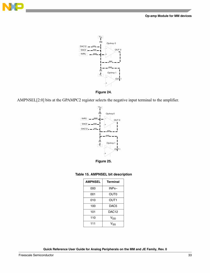
AMPNSEL[2:0] bits at the GPAMPC2 register selects the negative input terminal to the amplifier.
Figure 25.
Table 15. AMPNSEL bit description
AMPNSEL Terminal
000 INPx–
001 OUT0
010 OUT1
100 DAC5
101 DAC12
110 VDD
111 VSS
+
–
+
–
OpAmp 0
OpAmp 1
OUT 0
OUT 1
001
010
000
DAC5
DAC12
100
101
INP0+
VDD
110
Vss
111
+
–
+
–
OpAmp 0
OpAmp 1
OUT 0
OUT 1
DAC5
DAC12
INP0–
VDD
Vss
111
000
100
101001
010
110
Freescale Semiconductor 33
Op-amp Module for MM devices
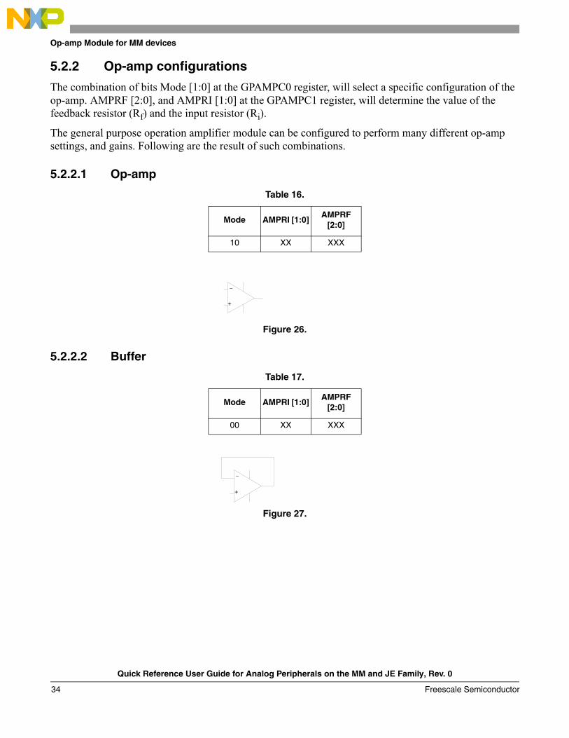
5.2.2 Op-amp configurations
The combination of bits Mode [1:0] at the GPAMPC0 register, will select a specific configuration of the op-amp. AMPRF [2:0], and AMPRI [1:0] at the GPAMPC1 register, will determine the value of the feedback resistor (Rf) and the input resistor (Ri).
The general purpose operation amplifier module can be configured to perform many different op-amp settings, and gains. Following are the result of such combinations.
5.2.2.1 Op-amp
Figure 26.
5.2.2.2 Buffer
Figure 27.
Table 16.
Mode AMPRI [1:0]AMPRF
[2:0]
10 XX XXX
Table 17.
Mode AMPRI [1:0]AMPRF
[2:0]
00 XX XXX
+
–
+
–
Quick Reference User Guide for Analog Peripherals on the MM and JE Family, Rev. 0
Freescale Semiconductor34

Op-amp Module for MM devices
5.2.2.3 Inverting programmable gainTable 18. Inverting Programmable Gain
Mode AMPRI [1:0]AMPRF
[2:0]Ri Rf Gain
01 00 000 1R —
01 00 001 1R 3R 3
01 00 010 1R 5R 5
01 00 011 1R 8R 8
01 00 100 1R 12R 12
01 00 101 1R 16R 16
01 00 110 1R —
01 00 111 1R —
01 01 000 2R —
01 01 001 2R 2R 1
01 01 010 2R 4R 2
01 01 011 2R 7R 7/2
01 01 100 2R 11R 11/2
01 01 101 2R 15R 15/2
01 01 110 2R —
01 01 111 2R —
⎟⎟⎠
⎞⎜⎜⎝
⎛−=
i
fINO R
RVV
⎟⎟⎠
⎞⎜⎜⎝
⎛=
i
f
RR
Gain
Quick Reference User Guide for Analog Peripherals on the MM and JE Family, Rev. 0
Freescale Semiconductor 35

Op-amp Module for MM devices
Figure 28.
Figure 29.
Table 19. Non–Inverting Programmable Gain
Mode AMPRI [1:0] AMPRF[2:0] Ri Rf Gain
11 00 000 1R –
11 00 001 1R 3R 4
11 00 010 1R 5R 6
11 00 011 1R 8R 9
11 00 100 1R 12R 13
11 00 101 1R 16R 17
11 00 110 1R –
11 00 111 1R –
11 01 000 2R –
11 01 001 2R 2R 2
11 01 010 2R 4R 3
11 01 011 2R 7R 9/2
11 01 100 2R 11R 13/2
11 01 101 2R 15R 17/2
11 01 110 2R –
11 01 111 2R –
Ri
Rf
+
–
VIN
⎟⎟⎠
⎞⎜⎜⎝
⎛+=
i
fRR
1 Gain
⎟⎟⎠
⎞⎜⎜⎝
⎛+=
i
fINO R
R1VV
Quick Reference User Guide for Analog Peripherals on the MM and JE Family, Rev. 0
Freescale Semiconductor36
Op-amp Module for MM devices
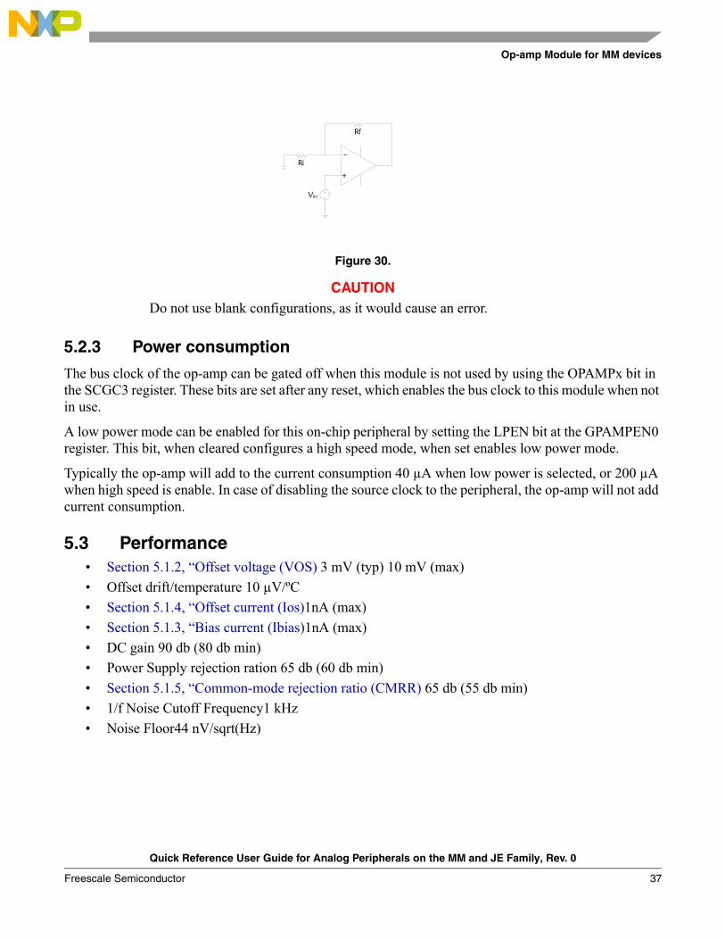
Figure 30.
CAUTIONDo not use blank configurations, as it would cause an error.
5.2.3 Power consumption
The bus clock of the op-amp can be gated off when this module is not used by using the OPAMPx bit in the SCGC3 register. These bits are set after any reset, which enables the bus clock to this module when not in use.
A low power mode can be enabled for this on-chip peripheral by setting the LPEN bit at the GPAMPEN0 register. This bit, when cleared configures a high speed mode, when set enables low power mode.
Typically the op-amp will add to the current consumption 40 µA when low power is selected, or 200 µA when high speed is enable. In case of disabling the source clock to the peripheral, the op-amp will not add current consumption.
5.3 Performance • Section 5.1.2, “Offset voltage (VOS) 3 mV (typ) 10 mV (max)• Offset drift/temperature 10 µV/ºC• Section 5.1.4, “Offset current (Ios)1nA (max)• Section 5.1.3, “Bias current (Ibias)1nA (max)• DC gain 90 db (80 db min)• Power Supply rejection ration 65 db (60 db min)• Section 5.1.5, “Common-mode rejection ratio (CMRR) 65 db (55 db min)• 1/f Noise Cutoff Frequency1 kHz• Noise Floor44 nV/sqrt(Hz)
Ri
Rf
+
–
VIN
Quick Reference User Guide for Analog Peripherals on the MM and JE Family, Rev. 0
Freescale Semiconductor 37
TRIAMP for MM devices
6 TRIAMP for MM devicesIn industry, DC current signals are often used in preference to DC voltage signals as analog representations of physical quantities. Current-sensing instruments typically have low input impedances, while voltage sensing instruments have high ones. Low impedances provide greater noise immunity.
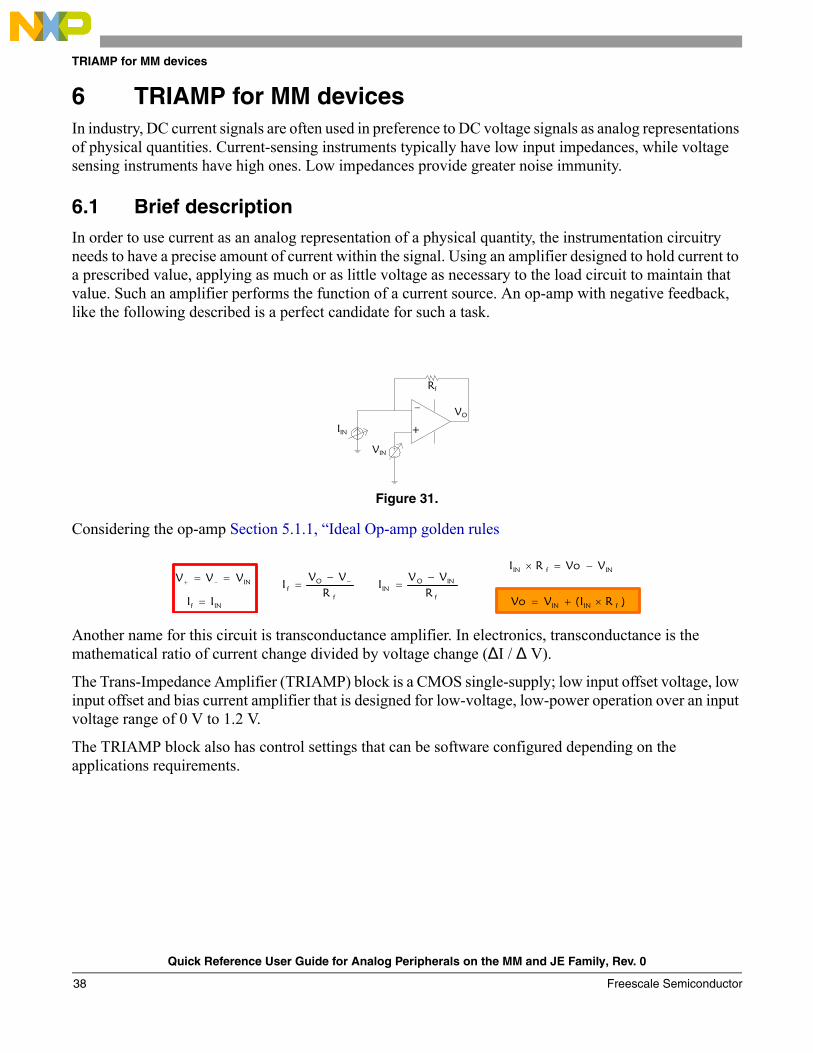
6.1 Brief descriptionIn order to use current as an analog representation of a physical quantity, the instrumentation circuitry needs to have a precise amount of current within the signal. Using an amplifier designed to hold current to a prescribed value, applying as much or as little voltage as necessary to the load circuit to maintain that value. Such an amplifier performs the function of a current source. An op-amp with negative feedback, like the following described is a perfect candidate for such a task.
Figure 31.
Considering the op-amp Section 5.1.1, “Ideal Op-amp golden rules
Another name for this circuit is transconductance amplifier. In electronics, transconductance is the mathematical ratio of current change divided by voltage change (ΔI / Δ V).
The Trans-Impedance Amplifier (TRIAMP) block is a CMOS single-supply; low input offset voltage, low input offset and bias current amplifier that is designed for low-voltage, low-power operation over an input voltage range of 0 V to 1.2 V.
The TRIAMP block also has control settings that can be software configured depending on the applications requirements.
+
– VO
Rf
VIN
IIN
INf II =
INVVV == −+
f
Of R
VVI −−
=INfIN VVoRI −=×
f
INOIN R
VVI
−=
)RI(VVo fININ ×+=
Quick Reference User Guide for Analog Peripherals on the MM and JE Family, Rev. 0
Freescale Semiconductor38
DAC for MM and JE devices
6.2 Performance • Section 5.1.2, “Offset voltage (VOS) 3 mV (typ) 10 mV (max)• Offset drift/temperature 10 mV/ºC• Section 5.1.4, “Offset current (Ios) 270 pA (max)• Section 5.1.3, “Bias current (Ibias) 300 pA (max)• DC Open Loop Voltage Gain (RL=20KΩ) 80 db • Power Supply Rejection 70db (60 db min)• Section 5.1.5, “Common-mode rejection ratio (CMRR) 70 db (60 db min)• 1/f Noise Cutoff Frequency1 kHz• Noise Floor44 nV/sqrt (Hz)
7 DAC for MM and JE devicesA Digital to Analog converter (DAC) is a very powerful module that allows to provide a voltage output from a given digital value.
7.1 Brief descriptionThe MM family provides one 12-bit DAC module that operates from 1.8 V to 3.6 V. Includes a 16-word data buffer for the output that can be used in different modes:
• Buffer Normal Mode: The buffer is set as a circular buffer. The output will be from the first word (DACDATA0) or the register pointed by the read pointer and move to the next on each trigger. Once it reaches the top pointer or the last word (DACDATA15) it will go back to the first word.
Quick Reference User Guide for Analog Peripherals on the MM and JE Family, Rev. 0
Freescale Semiconductor 39
DAC for MM and JE devices
Figure 32.
void vfnDACV1Initialization(void) DACS = 0x00; /** Clear the status register since one of the flags is set on POR */ DACC0 |= (DACC0_DACRFS_MASK | DACC0_DACTSEL_MASK | DACC0_DACTIE_MASK); /** Default configuration */ /** DACRFS = External Reference */ /** DACTSEL = SW Trigger */ /** LPEN = Low Power */ /** Interrupt source = Top pointer */ DACC1 |= DACC1_DACBFE_MASK; /* Enable Buffered mode and select Normal Mode since is the default */ DACC0 |= DACC0_DACEN_MASK; /* Enable the module */
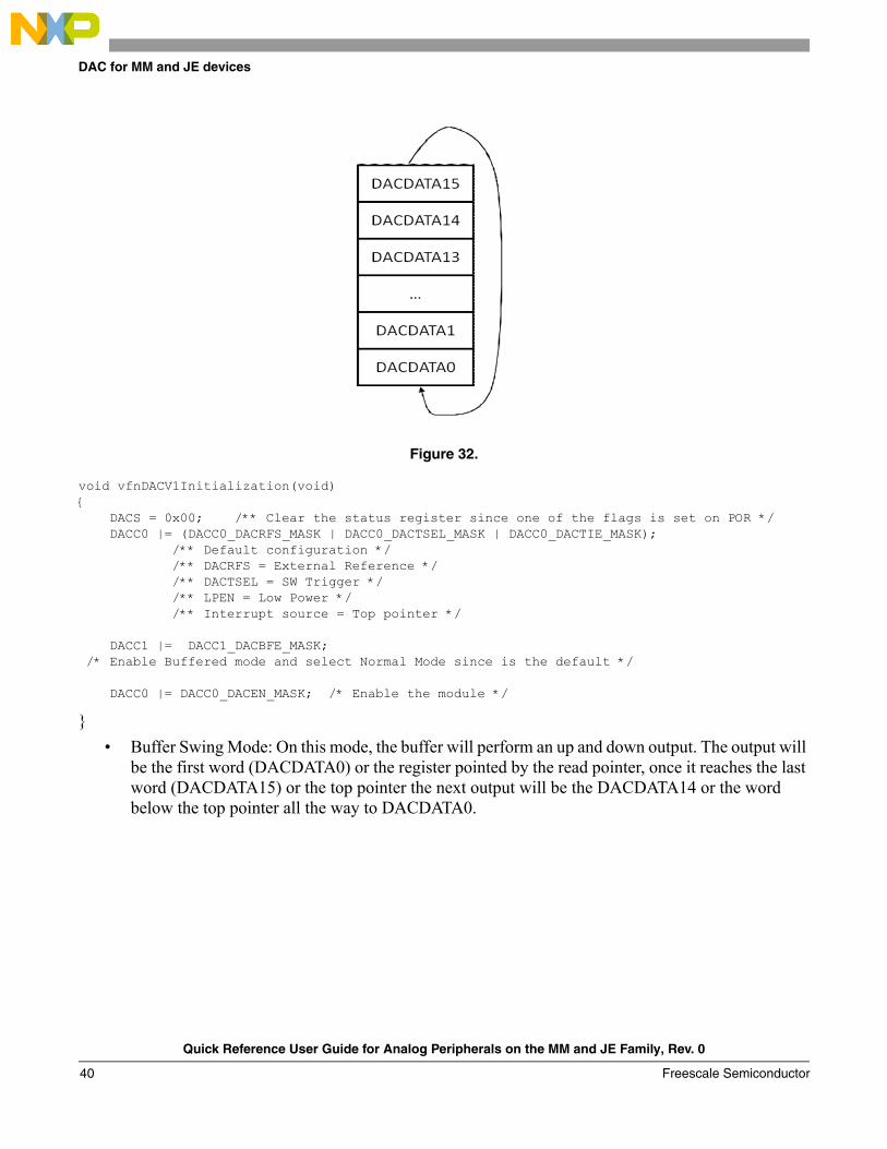
• Buffer Swing Mode: On this mode, the buffer will perform an up and down output. The output will
be the first word (DACDATA0) or the register pointed by the read pointer, once it reaches the last word (DACDATA15) or the top pointer the next output will be the DACDATA14 or the word below the top pointer all the way to DACDATA0.
Quick Reference User Guide for Analog Peripherals on the MM and JE Family, Rev. 0
Freescale Semiconductor40
DAC for MM and JE devices
Figure 33.
void vfnDACV1Initialization(void) DACS = 0x00; /** Clear the status register since one of the flags is set on POR */ DACC0 |= (DACC0_DACRFS_MASK | DACC0_DACTSEL_MASK | DACC0_DACTIE_MASK); /** Default configuration */ /** DACRFS = External Reference */ /** DACTSEL = SW Trigger */ /** LPEN = Low Power */ /** Interrupt source = Top pointer */ DACC1 |= DACC1_DACBFMD0_MASK | DACC1_DACBFE_MASK; /* Enable Buffered mode and select Swing Mode */ DACC0 |= DACC0_DACEN_MASK; /* Enable the module */
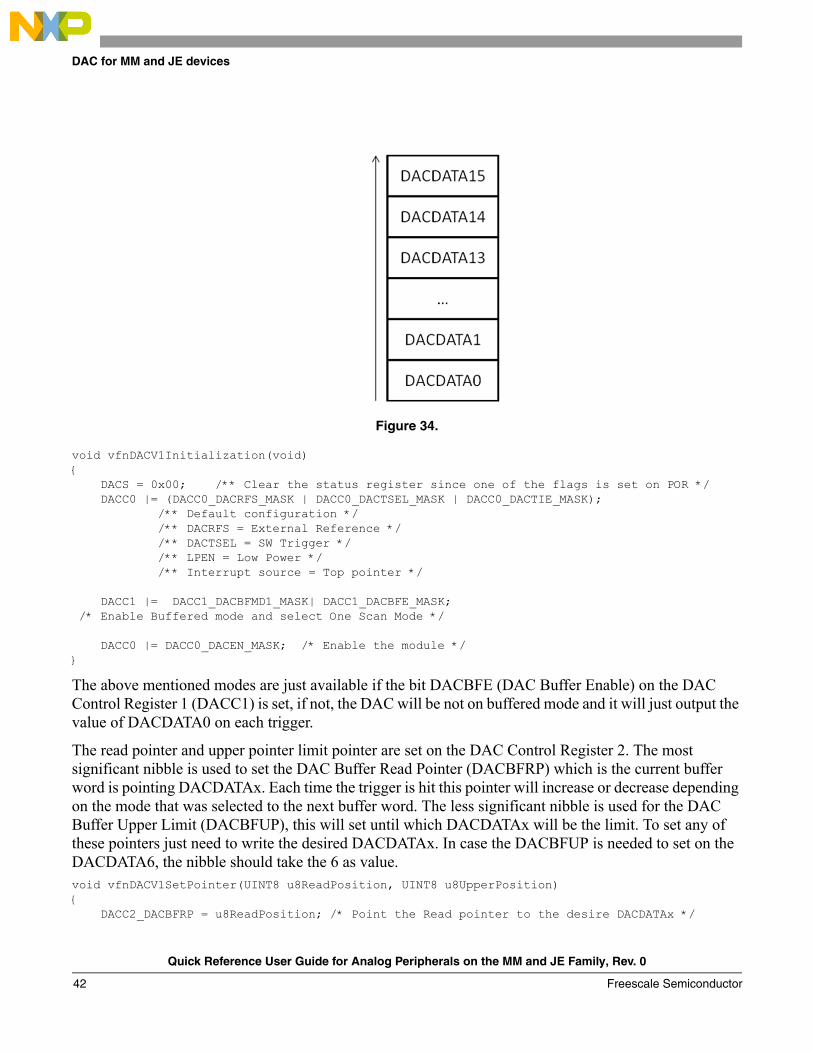
• Buffer One-Time Scan Mode: The buffer will perform a read from DACDATA0 or the word pointed by the read register to the top and it will stop. In this case the read pointer should be refreshed for getting new output.
Quick Reference User Guide for Analog Peripherals on the MM and JE Family, Rev. 0
Freescale Semiconductor 41
DAC for MM and JE devices
Figure 34.
void vfnDACV1Initialization(void) DACS = 0x00; /** Clear the status register since one of the flags is set on POR */ DACC0 |= (DACC0_DACRFS_MASK | DACC0_DACTSEL_MASK | DACC0_DACTIE_MASK); /** Default configuration */ /** DACRFS = External Reference */ /** DACTSEL = SW Trigger */ /** LPEN = Low Power */ /** Interrupt source = Top pointer */ DACC1 |= DACC1_DACBFMD1_MASK| DACC1_DACBFE_MASK; /* Enable Buffered mode and select One Scan Mode */ DACC0 |= DACC0_DACEN_MASK; /* Enable the module */
The above mentioned modes are just available if the bit DACBFE (DAC Buffer Enable) on the DAC Control Register 1 (DACC1) is set, if not, the DAC will be not on buffered mode and it will just output the value of DACDATA0 on each trigger.
The read pointer and upper pointer limit pointer are set on the DAC Control Register 2. The most significant nibble is used to set the DAC Buffer Read Pointer (DACBFRP) which is the current buffer word is pointing DACDATAx. Each time the trigger is hit this pointer will increase or decrease depending on the mode that was selected to the next buffer word. The less significant nibble is used for the DAC Buffer Upper Limit (DACBFUP), this will set until which DACDATAx will be the limit. To set any of these pointers just need to write the desired DACDATAx. In case the DACBFUP is needed to set on the DACDATA6, the nibble should take the 6 as value.void vfnDACV1SetPointer(UINT8 u8ReadPosition, UINT8 u8UpperPosition) DACC2_DACBFRP = u8ReadPosition; /* Point the Read pointer to the desire DACDATAx */
Quick Reference User Guide for Analog Peripherals on the MM and JE Family, Rev. 0
Freescale Semiconductor42
DAC for MM and JE devices
DACC2_DACBFUP = u8UpperPosition; /* Point the Upper pointer to the desire DACDATAx */
The DAC provides 4 different watermarks that are used to acknowledge when the read pointer is 1, 2, 3 or 4 words to away to reach the upper limit. These watermarks can be selected on the DACBFWM on the DACC1.void vfnDACV1Initialization(void) DACS = 0x00; /** Clear the status register since one of the flags is set on POR */ DACC0 |= (DACC0_DACRFS_MASK | DACC0_DACTSEL_MASK | DACC0_DACWIE_MASK); /** Default configuration */ /** DACRFS = External Reference */ /** DACTSEL = SW Trigger */ /** LPEN = Low Power */ /** Interrupt source = Watermark */ DACC1 |= DACC1_DACBFWM1_MASK | DACC1_DACBFE_MASK; /* Enable Buffered mode and select Normal Mode and select the watermark for 3 words*/ DACC0 |= DACC0_DACEN_MASK; /* Enable the module */
The output voltage is given by the following formula:Vout = 1/4096 Vin * DACDATx[11:0]
Where the “Vin” could be from 2 different sources selectable on with the DACRFS bit on DACC0:• Vext: which is corresponds to the MCU VDD.• Vint: Takes the VREF voltage as the reference.
void vfnDACV1Initialization(void) DACS = 0x00; /** Clear the status register since one of the flags is set on POR */ DACC0 |= (DACC0_DACRFS_MASK | DACC0_DACTSEL_MASK | DACC0_DACTIE_MASK); /** Default configuration */ /** DACRFS = External Reference */ /** DACTSEL = SW Trigger */ /** LPEN = Low Power */ /** Interrupt source = Top pointer */ DACC1 |= DACC1_DACBFE_MASK; /* Enable Buffered mode and select Normal Mode since is the default */ DACC0 |= DACC0_DACEN_MASK; /* Enable the module */void vfnDACV1Initialization(void) DACS = 0x00; /** Clear the status register since one of the flags is set on POR */ DACC0 |= (DACC0_DACTSEL_MASK | DACC0_DACTIE_MASK); /** Default configuration */ /** DACRFS = Internal Reference */ /** DACTSEL = SW Trigger */ /** LPEN = Low Power */ /** Interrupt source = Top pointer */ DACC1 |= DACC1_DACBFE_MASK; /* Enable Buffered mode and select Normal Mode since is the default */ DACC0 |= DACC0_DACEN_MASK; /* Enable the module */
Quick Reference User Guide for Analog Peripherals on the MM and JE Family, Rev. 0
Freescale Semiconductor 43
DAC for MM and JE devices
The DAC has 2 trigger sources which the user can select with the DACTSEL bit on DAC Control Register 0 (DACC0):
• Hardware trigger: This is via the Programmable Delay Block (PDB), which will help to synchronize the DAC trigger with ADC reads. See the Section 3, “PDB module for MM and JE devices for further information.
• Software trigger: This is activated each time DACSTRG bit is set on DACC0. For each time DACSTRG is set a word of the buffer will be converted to the equivalent voltage and the read pointer will move to the next word. In case the application needs to output the 16 words of the buffer the SW trigger should be set 16 times.
The DAC has 3 available interrupt flags which correspond to 3 different sources. These are located on the status register DACS:
• DAC buffer Watermark (DACWM): There are 4 watermark options available that can be selected on the DACC1 register. Once the read pointer reaches the selected watermark it generates the interruption.
• DAC buffer read pointer top position (DACRPT): Once the read pointer reaches the top it will be back to DACDATA0 (depending on the Buffer mode selected), at this time the Top position buffer will be set.
• DAC buffer read pointer bottom position (DACRPB): When the read pointer reaches the upper pointer this interruption will be set.
7.2 Settling timeThe change from a binary value to the output voltage on a DAC cannot be instantaneous therefore it takes some time for the resistive ladder to acquire the correct voltage. The time it takes from the moment the value is set and the correct output voltage is reached is called Settling time. Faster is the settling time the waveform or output voltage will be more accurate.
The 12-bit DAC of the MM family provides a settling time of 1μs as typical when using the High Power mode and 5μs when using the low power mode this allows the application to get a better performance and a better resolution on the final analog output.
The Low Power and High Power modes can be selected with the LPEN bit on DACC0.
7.3 Power consumption The MM family is targeted for low power Home Medical devices, so the peripheral should meet the requirements in the ANPERPHQRUG and provide a full low power mode to achieve the goal of having the less current consumption possible.
The 12-bit DAC provides modes for using on low power modes. The maximum current consumption of the DAC on low power is 100 μA.
If the DAC will not be used on the application it can be disabled using the clock gating. When the application enters the STOP3 mode, the DAC operation remains normal and the output voltage is held by the module.
Quick Reference User Guide for Analog Peripherals on the MM and JE Family, Rev. 0
Freescale Semiconductor44
Differential Input – Single Output
When the application enters to STOP2, the module is disabled and no output voltage is generated.
8 Differential Input – Single Output An op-amp with no feedback is already a differential amplifier, however, its gain cannot be controlled, because it is generally too high for any practical use.
Applications with negative feedback has result on the loss of one of the amplifier inputs. Therefore the resulting amplifier is only good for amplifying a Single Input – Single Output applications.
The following section will explain how to build a Differential Input – Single Output amplifier. Although there are several techniques that can be used for such configuration, this document only boards the most common ones.
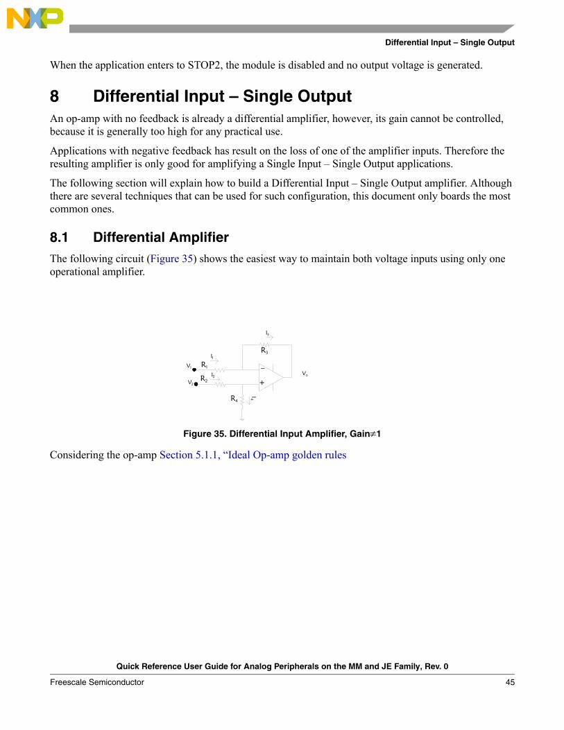
8.1 Differential AmplifierThe following circuit (Figure 35) shows the easiest way to maintain both voltage inputs using only one operational amplifier.
Figure 35. Differential Input Amplifier, Gain≠1
Considering the op-amp Section 5.1.1, “Ideal Op-amp golden rules
+
–
I1
V1
V2
R1
R2
R4
R3
I2
I3
I4
Vo
Quick Reference User Guide for Analog Peripherals on the MM and JE Family, Rev. 0
Freescale Semiconductor 45
Differential Input – Single Output
Figure 36.
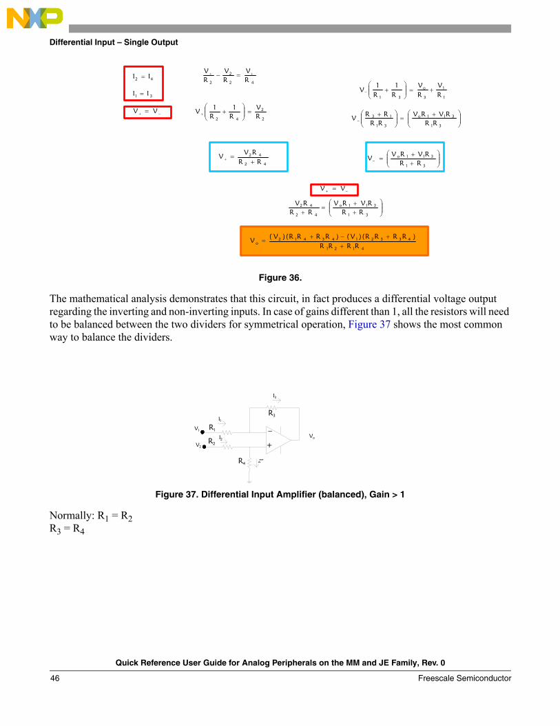
The mathematical analysis demonstrates that this circuit, in fact produces a differential voltage output regarding the inverting and non-inverting inputs. In case of gains different than 1, all the resistors will need to be balanced between the two dividers for symmetrical operation, Figure 37 shows the most common way to balance the dividers.
Figure 37. Differential Input Amplifier (balanced), Gain > 1
Normally: R1 = R2 R3 = R4
−+ = VV
42 II =
31 II =
42
2
2 RV
RV
RV ++ =−
2
2
42 RV
R1
R1V =⎟⎟⎠
⎞⎜⎜⎝
⎛++
1
1
3
o
31 RV
RV
R1
R1
V +=⎟⎟⎠
⎞⎜⎜⎝
⎛+−
⎟⎟⎠
⎞⎜⎜⎝
⎛ +=⎟⎟⎠
⎞⎜⎜⎝
⎛ +−
31
311o
31
13
RRRVRV
RRRR
V
⎟⎟⎠
⎞⎜⎜⎝
⎛++=−
31
311o
RRRVRV
V
−+ = VV
⎟⎟⎠
⎞⎜⎜⎝
⎛++=
+ 31
311o
42
42
RRRVRV
RRRV
42
42
RRRV
V+
=+
4121
4332143412o RRRR
)RRRR)(V()RRRR)(V(V+
+−+=
+
–
I1
V1
V2
R1
R2
R4
R3
I2
I3
I4
Vo
Quick Reference User Guide for Analog Peripherals on the MM and JE Family, Rev. 0
Freescale Semiconductor46
Differential Input – Single Output
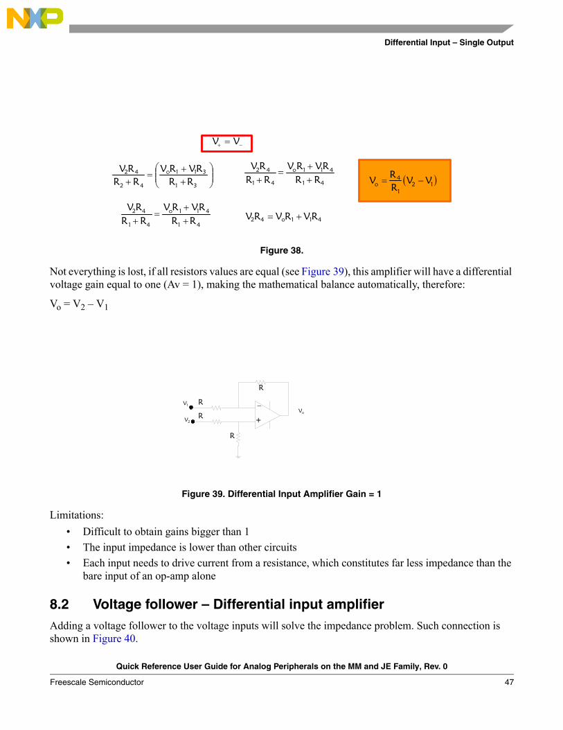
Figure 38.
Not everything is lost, if all resistors values are equal (see Figure 39), this amplifier will have a differential voltage gain equal to one (Av = 1), making the mathematical balance automatically, therefore:
Vo = V2 – V1
Figure 39. Differential Input Amplifier Gain = 1
Limitations:• Difficult to obtain gains bigger than 1 • The input impedance is lower than other circuits• Each input needs to drive current from a resistance, which constitutes far less impedance than the
bare input of an op-amp alone
8.2 Voltage follower – Differential input amplifier Adding a voltage follower to the voltage inputs will solve the impedance problem. Such connection is shown in Figure 40.
( )121
4o VV
RRV −=
−+ = VV
⎟⎟⎠
⎞⎜⎜⎝
⎛++=
+ 31
311o
42
42
RRRVRV
RRRV
41
411o
41
42
RRRVRV
RRRV
++
=+
41
411o
41
42
RRRVRV
RRRV
++=
+
411o42 RVRVRV +=
+
–V1
V2
R
R
R
R
Vo
Quick Reference User Guide for Analog Peripherals on the MM and JE Family, Rev. 0
Freescale Semiconductor 47
Differential Input – Single Output
Figure 40. Voltage follower – Differential Input Amplifier Gain = 1
Now the input voltages V1 and V2 are connected straight to the inputs of two voltage follower op-amps, giving very high impedance to the Differential Amplifier inputs. The op-amps on the left now handle the driving current, providing a trustable voltage source to the Differential Amplifier.
Although adding two more operational amplifier increases cost and the complexity of the circuit, the benefits of doing it, solves important faults.
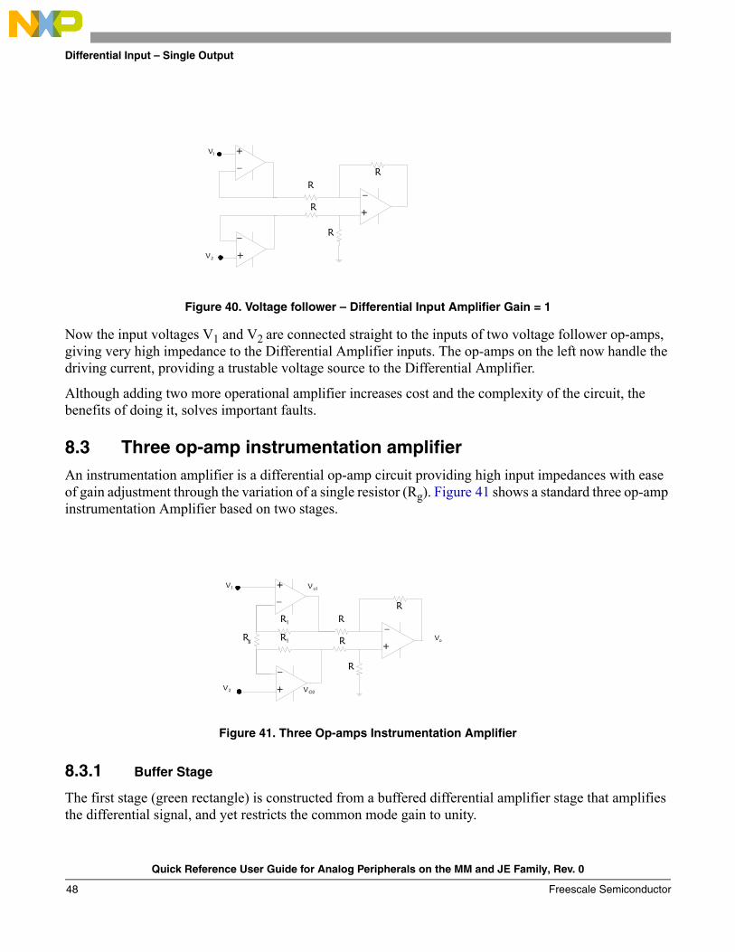
8.3 Three op-amp instrumentation amplifierAn instrumentation amplifier is a differential op-amp circuit providing high input impedances with ease of gain adjustment through the variation of a single resistor (Rg). Figure 41 shows a standard three op-amp instrumentation Amplifier based on two stages.
Figure 41. Three Op-amps Instrumentation Amplifier
8.3.1 Buffer Stage
The first stage (green rectangle) is constructed from a buffered differential amplifier stage that amplifies the differential signal, and yet restricts the common mode gain to unity.
+
–
V1
V2
R
R
R
R
+
–
+
–
+
–
V1
V2
R
R
R
R
+
–
+
–
Vo
R1
R1Rg
Vo1
VO2
Quick Reference User Guide for Analog Peripherals on the MM and JE Family, Rev. 0
Freescale Semiconductor48

Differential Input – Single Output
Figure 42. Buffer stage
Figure 43.
The buffer stage op-amp A1 and A2 negative feedback causes the top of Rg voltage to be equal to V1. Likewise, the voltage at the bottom of Rg is held to a value equal to V2.
This establishes a voltage drop across Rg equal to the voltage difference between V1 and V2. That voltage drop causes a current through Rg, and since the feedback loops of the two input op-amps draw no current, that same amount of current through Rg must be going through the two "R1" resistors above and below it.
Quick Reference User Guide for Analog Peripherals on the MM and JE Family, Rev. 0
Freescale Semiconductor 49

Differential Input – Single Output
8.3.2 Differential stage
The next stage (orange rectangle) is a single op-amp differential amplifier explained in Section 9.1, “How to build your differential input – differential output amplifier
Figure 44. Differential stage
Figure 45.
8.3.3 Instrumentation Amplifier limitations • Saturate supply rails by big gains at the buffer stage amplifiers• AC coupling without providing a DC return path• Single supply circuits have less operation range than dual-supply
8.3.4 Instrumentation Amplifier advantages • High input impedance• Gain adjustment through the variation of a single resistor• Noise immunity
1o2oo VVV −=
( ) ( )⎟⎟⎠⎞
⎜⎜⎝
⎛−⎟⎟⎠
⎞⎜⎜⎝
⎛++−⎟⎟⎠
⎞⎜⎜⎝
⎛−⎟⎟⎠
⎞⎜⎜⎝
⎛++= 21
1112
12o VV
RgR1VVV
RgR1VV
( )121
o VVRgR2
1V −⎟⎟⎠
⎞⎜⎜⎝
⎛+=
Quick Reference User Guide for Analog Peripherals on the MM and JE Family, Rev. 0
Freescale Semiconductor50
Differential Input – Differential Output advantages
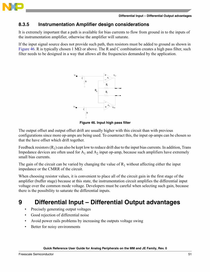
8.3.5 Instrumentation Amplifier design considerations
It is extremely important that a path is available for bias currents to flow from ground in to the inputs of the instrumentation amplifier, otherwise the amplifier will saturate.
If the input signal source does not provide such path, then resistors must be added to ground as shown in Figure 46. R is typically chosen 1 MΩ or above. The R and C combination creates a high pass filter, such filter needs to be designed in a way that allows all the frequencies demanded by the application.
Figure 46. Input high pass filter
The output offset and output offset drift are usually higher with this circuit than with previous configurations since more op-amps are being used. To counteract this, the input op-amps can be chosen so that the have offset which drift together.
Feedback resistors (R1) can also be kept low to reduce drift due to the input bias currents. In addition, Trans Impedance devices are often used for A1 and A2 input op-amp, because such amplifiers have extremely small bias currents.
The gain of the circuit can be varied by changing the value of R1 without affecting either the input impedance or the CMRR of the circuit.
When choosing resistor values, it is convenient to place all of the circuit gain in the first stage of the amplifier (buffer stage) because at this state, the instrumentation circuit amplifies the differential input voltage over the common mode voltage. Developers must be careful when selecting such gain, because there is the possibility to saturate the differential inputs.
9 Differential Input – Differential Output advantages • Precisely generating output voltages• Good rejection of differential noise• Avoid power rails problems by increasing the outputs voltage swing• Better for noisy environments
A1
+
–
R1
Rg
Vo1
A2+
–
R1
VO2V2
V1
C
R
C
R
Quick Reference User Guide for Analog Peripherals on the MM and JE Family, Rev. 0
Freescale Semiconductor 51
Differential Input – Differential Output advantages
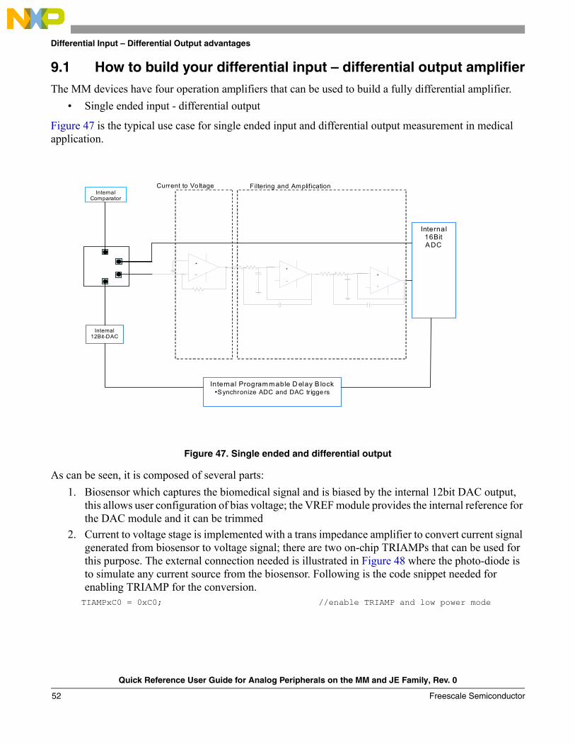
9.1 How to build your differential input – differential output amplifierThe MM devices have four operation amplifiers that can be used to build a fully differential amplifier.
• Single ended input - differential output
Figure 47 is the typical use case for single ended input and differential output measurement in medical application.
Figure 47. Single ended and differential output
As can be seen, it is composed of several parts: 1. Biosensor which captures the biomedical signal and is biased by the internal 12bit DAC output,
this allows user configuration of bias voltage; the VREF module provides the internal reference for the DAC module and it can be trimmed
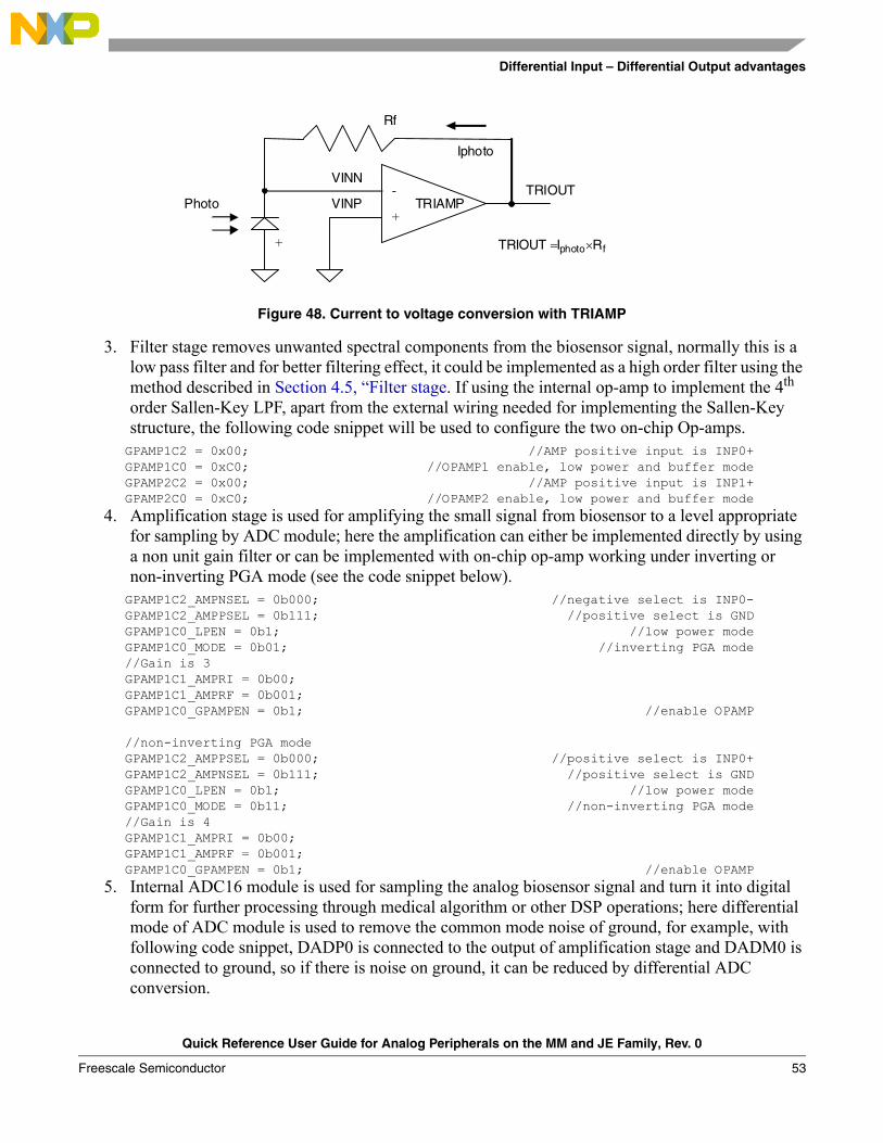
2. Current to voltage stage is implemented with a trans impedance amplifier to convert current signal generated from biosensor to voltage signal; there are two on-chip TRIAMPs that can be used for this purpose. The external connection needed is illustrated in Figure 48 where the photo-diode is to simulate any current source from the biosensor. Following is the code snippet needed for enabling TRIAMP for the conversion.TIAMPxC0 = 0xC0; //enable TRIAMP and low power mode
Internal 16Bit A DC
Internal 12Bit-DAC
Internal Programmable D elay B lock •Synchronize ADC and DAC tr igge rs
Internal Comparator
Current to Vo ltage Filtering and Amplification
+
-
+
-
+
-
Quick Reference User Guide for Analog Peripherals on the MM and JE Family, Rev. 0
Freescale Semiconductor52
Differential Input – Differential Output advantages
Figure 48. Current to voltage conversion with TRIAMP
3. Filter stage removes unwanted spectral components from the biosensor signal, normally this is a low pass filter and for better filtering effect, it could be implemented as a high order filter using the method described in Section 4.5, “Filter stage. If using the internal op-amp to implement the 4th order Sallen-Key LPF, apart from the external wiring needed for implementing the Sallen-Key structure, the following code snippet will be used to configure the two on-chip Op-amps.GPAMP1C2 = 0x00; //AMP positive input is INP0+GPAMP1C0 = 0xC0; //OPAMP1 enable, low power and buffer modeGPAMP2C2 = 0x00; //AMP positive input is INP1+GPAMP2C0 = 0xC0; //OPAMP2 enable, low power and buffer mode
4. Amplification stage is used for amplifying the small signal from biosensor to a level appropriate for sampling by ADC module; here the amplification can either be implemented directly by using a non unit gain filter or can be implemented with on-chip op-amp working under inverting or non-inverting PGA mode (see the code snippet below).GPAMP1C2_AMPNSEL = 0b000; //negative select is INP0-GPAMP1C2_AMPPSEL = 0b111; //positive select is GNDGPAMP1C0_LPEN = 0b1; //low power modeGPAMP1C0_MODE = 0b01; //inverting PGA mode//Gain is 3GPAMP1C1_AMPRI = 0b00;GPAMP1C1_AMPRF = 0b001;GPAMP1C0_GPAMPEN = 0b1; //enable OPAMP
//non-inverting PGA modeGPAMP1C2_AMPPSEL = 0b000; //positive select is INP0+GPAMP1C2_AMPNSEL = 0b111; //positive select is GNDGPAMP1C0_LPEN = 0b1; //low power modeGPAMP1C0_MODE = 0b11; //non-inverting PGA mode//Gain is 4GPAMP1C1_AMPRI = 0b00;GPAMP1C1_AMPRF = 0b001;GPAMP1C0_GPAMPEN = 0b1; //enable OPAMP
5. Internal ADC16 module is used for sampling the analog biosensor signal and turn it into digital form for further processing through medical algorithm or other DSP operations; here differential mode of ADC module is used to remove the common mode noise of ground, for example, with following code snippet, DADP0 is connected to the output of amplification stage and DADM0 is connected to ground, so if there is noise on ground, it can be reduced by differential ADC conversion.
-
+
Rf
+
VINN
VINP TRIOUT
Iphoto
fphoto RITRIOUT ×=
Photo TRIAMP
Quick Reference User Guide for Analog Peripherals on the MM and JE Family, Rev. 0
Freescale Semiconductor 53

References
ADCCFG1 = 0x3C; //normal mode, bus clock/2, long sample time, 16bit conversionADCCFG2 = 0x00; //normal conversion, default long sample timeADCSC2 = 0x40; //hardware trigger, VREFH/VREFL as referenceADCSC3 = 0x0C; //continuous mode, 4 sample averageADCSC1A = 0x60; //ADC interrupt enable, differential mode, DADP0/DADM0
6. Internal PDB module provides synchronized triggering pulses for ADC and DAC, see Section 3, “PDB module for MM and JE devices for sample code snippet.
10 ReferencesANQRUGSW — Referenced Software
11 Revision HistoryTable 20. Revision History
DateRevision
LevelDescription
PageNumber(s)
07/2010 0 Initial public release N/A
Quick Reference User Guide for Analog Peripherals on the MM and JE Family, Rev. 0
Freescale Semiconductor54

Document Number: ANPERIPHQRUGRev. 007/2010
How to Reach Us:
Home Page:www.freescale.com
Web Support:http://www.freescale.com/support
USA/Europe or Locations Not Listed:Freescale Semiconductor, Inc.Technical Information Center, EL5162100 East Elliot RoadTempe, Arizona 85284+1-800-521-6274 or +1-480-768-2130www.freescale.com/support
Europe, Middle East, and Africa:Freescale Halbleiter Deutschland GmbHTechnical Information CenterSchatzbogen 781829 Muenchen, Germany+44 1296 380 456 (English)+46 8 52200080 (English)+49 89 92103 559 (German)+33 1 69 35 48 48 (French)www.freescale.com/support
Japan:Freescale Semiconductor Japan Ltd.HeadquartersARCO Tower 15F1-8-1, Shimo-Meguro, Meguro-ku,Tokyo 153-0064Japan0120 191014 or +81 3 5437 [email protected]
Asia/Pacific:Freescale Semiconductor China Ltd.Exchange Building 23FNo. 118 Jianguo RoadChaoyang DistrictBeijing 100022 China +86 10 5879 [email protected]
For Literature Requests Only:Freescale Semiconductor Literature Distribution Center1-800-441-2447 or 303-675-2140Fax: [email protected]
Information in this document is provided solely to enable system and software implementers to use Freescale Semiconductor products. There are no express or implied copyright licenses granted hereunder to design or fabricate any integrated circuits or integrated circuits based on the information in this document.
Freescale Semiconductor reserves the right to make changes without further notice to any products herein. Freescale Semiconductor makes no warranty, representation or guarantee regarding the suitability of its products for any particular purpose, nor does Freescale Semiconductor assume any liability arising out of the application or use of any product or circuit, and specifically disclaims any and all liability, including without limitation consequential or incidental damages. “Typical” parameters that may be provided in Freescale Semiconductor data sheets and/or specifications can and do vary in different applications and actual performance may vary over time. All operating parameters, including “Typicals”, must be validated for each customer application by customer’s technical experts. Freescale Semiconductor does not convey any license under its patent rights nor the rights of others. Freescale Semiconductor products are not designed, intended, or authorized for use as components in systems intended for surgical implant into the body, or other applications intended to support or sustain life, or for any other application in which the failure of the Freescale Semiconductor product could create a situation where personal injury or death may occur. Should Buyer purchase or use Freescale Semiconductor products for any such unintended or unauthorized application, Buyer shall indemnify and hold Freescale Semiconductor and its officers, employees, subsidiaries, affiliates, and distributors harmless against all claims, costs, damages, and expenses, and reasonable attorney fees arising out of, directly or indirectly, any claim of personal injury or death associated with such unintended or unauthorized use, even if such claim alleges that Freescale Semiconductor was negligent regarding the design or manufacture of the part.
RoHS-compliant and/or Pb-free versions of Freescale products have the functionality and electrical characteristics as their non-RoHS-compliant and/or non-Pb-free counterparts. For further information, see http://www.freescale.com or contact your Freescale sales representative.
For information on Freescale’s Environmental Products program, go to http://www.freescale.com/epp.
Freescale™ and the Freescale logo are trademarks of Freescale Semiconductor, Inc. All other product or service names are the property of their respective owners.© Freescale Semiconductor, Inc. 2010. All rights reserved.