qucs - a tutorial - github pagesguitorri.github.io/qucs-web/docs/ffmodels.pdf · transient domain...
TRANSCRIPT

Qucs
A Tutorial
Transient Domain Flip-Flop Models for Mixed-Mode Simulation
Mike Brinson
Copyright c© 2006 Mike Brinson <[email protected]>
Permission is granted to copy, distribute and/or modify this document under the terms ofthe GNU Free Documentation License, Version 1.1 or any later version published by theFree Software Foundation. A copy of the license is included in the section entitled ”GNUFree Documentation License”.

Introduction
One of the primary aims of the Qucs project is the development of a universal circuit simu-lator that allows circuit performance to be investigated from DC to microwave frequencies.Adding performance analysis in the digital domain makes Qucs a truly universal simula-tor. Qucs 0.0.8 was the first release to include digital simulation. Qucs digital simulationcentres around VHDL using the FreeHDL VHDL compiler to generate a machine code si-mulation of a circuit under test. Release 0.0.8 includes built-in models for the basic digitalgates and a number of the common sequential flip-flops. The Qucs gate models can beused in both digital and transient simulation. Unfortunately, the flip-flop models are onlyavailable in digital simulation. The current version of Qucs models flip-flops using VHDLand does not provide time domain models for transient simulation. This is an importantomission which limits the Qucs simulator mixed-mode simulation capabilities. Mixed-modesimulation is a term commonly employed to describe the simulation of circuits that con-tain both analogue and digital components. In the real world circuits are, of course, notsubdivided into neat boxes labelled analogue, S-parameter, digital or any other physicaldomain. So it is of some importance that Qucs device modelling be developed to allowcircuits consisting of a range of different analogue and digital components, to be simulatedat the same time. Normally such systems are simulated in the time domain using largesignal transient simulation. Performance data being both analogue and digital expressedin tabular or graphical form. This tutorial note presents a number of transient simulationmodels for flip-flops based on structural digital circuits, describes their use, and outlines anumber of example simulations derived from practical circuits.
Latches and flip-flops
Sequential digital devices generically known as flip-flops (SR, D, JK and T types) arecommonly classified into three major groups.
• Latches: basic or gated
• Pulse triggered flip-flops: master slave devices with or without data-lockout
• Edge-triggered flip-flops: leading or trailing edge triggered.
As the speed of electronic systems has increased so has the popularity of the single edge-triggered flip-flops over the slower master slave devices. Today most IC designs are basedon D type edge-triggered devices rather than the earlier JK master slave devices. Ourconcern here is the development of a consistant set of models that allow the common flip-flops to be modelled accurately, and reliably, in the transient time domain. In order tokeep these models simple the D gated and edge-triggered devices have been chosen as thefundamental building blocks for the transient domain Qucs models. Using basic Booleanlogic concepts it is straightforward to show that JK and T edge-triggered flip-flop modelscan be derived from the D flip-flop models.
1

The gated D latch
The circuit diagram for a gated D latch constructed from two input nand gates is shown inFig. 11. Outputs Q and not Q (QB in Fig. 1) are derived from the two cross coupled nandgates connected as a basic SR nand latch. Fig. 2 shows the performance characteristics forthis circuit. These were obtained using the simple test configuration shown in Fig. 3. Logicone digital signals are represented by 1V and logic 0 signals by 0V in the transient analysisdomain. Propagation delays through the various circuit gates can be set by changing thedelay time for each gate. Cross coupled gates are often a cause of simulation failure due tothe fact that DC analysis fails to converge to a stable solution at the start of a transientsimulation. One approach that helps to force a stable DC solution is to set Q and QB toknown values, say logic 0 and logic 1, at the start of a simulation. In circuits like the basicgated D latch shown in Fig. 1, where asynchronous set and reset inputs are not included,this is not possible. However, flip-flops with asynchronous set and reset inputs do allow thestate of a flip-flop to be determined at a given time in a simulation. In the examples thatfollow, whenever possible, the state of the latch or flip-flop devices is set at the start of asimulation. In the majority of the example circuits, device delays have also been set to zero.It therefore follows that most waveform plots show functional data rather than accuratetiming characteristics. In many mixed-mode simulations the digital elements present ina design are often modelled as functional devices whose primary task is to generate thesignals needed for the overall circuit to function. A more detailed discussion of the effectson transient simulation caused by including device timing delays is presented in a latersection of these notes.
&
Y3
&
Y4
Dtimes=20ns; 20ns
Ctimes=5ns; 5ns
&
Y2
&
Y1
&
Y5
transientsimulation
TR1Type=linStart=0Stop=100 ns
C
QB
Q
D
Figure 1: Gated D latch with digital signal generators D and C
1Richard S. Sandige, Modern Digital Design, 1990, McGraw-Hill International Editions.
2

0 2e-8 4e-8 6e-8 8e-8 1e-7 1.2e-7 1.4e-7 1.6e-7 1.8e-7 2e-7
0
1
time
D.V
t
0 2e-8 4e-8 6e-8 8e-8 1e-7 1.2e-7 1.4e-7 1.6e-7 1.8e-7 2e-7
0
1
time
C.V
t
0 2e-8 4e-8 6e-8 8e-8 1e-7 1.2e-7 1.4e-7 1.6e-7 1.8e-7 2e-7
0
1
time
Q.V
t
0 2e-8 4e-8 6e-8 8e-8 1e-7 1.2e-7 1.4e-7 1.6e-7 1.8e-7 2e-7
0
1
time
QB
.Vt
Figure 2: Gated D latch simulation waveforms
D Q
C Q
SUB1File=gated_d_latch.sch
D
CNum=2
transientsimulation
TR1Type=linStart=0Stop=200 ns
D
C
Q
QB
Figure 3: Gated D latch test circuit
3

Edge-triggered D type flip-flop
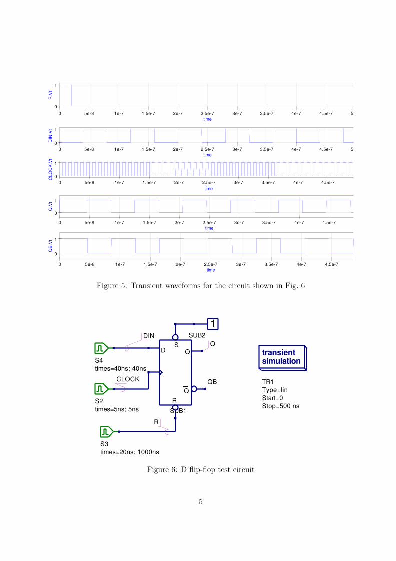
The schematic for a positive edge-triggered D flip-flop is shown in Fig. 42. Asynchronousset (SET) and reset (RESET) control inputs allow the flip-flop outputs Q and not Q (QBin Fig. 4) to be set to known values at the start of a simulation. The nand gates formingeach of the cross coupled SR latches have their delay times set at 0 ns. The edge-triggeredD device is a building block for both the JK and T types of flip-flop. A typical set oftransient simulation test results for the D flip-flop model are illustrated in Fig. 5. Thesewhere obtained using the basic test configuration shown in Fig. 6.
CLOCKNum=1
QB
Q
&
Y2
&
Y8
&
Y9
&
Y11
&
Y10
SET
DINNum=2
RESET
&
Y7
I2
CLOCK
SET
I3
DIN
I1
I0
QB
QRESET
Figure 4: Positive edge-triggered D flip-flop circuit
2David A. Hodges and Horace G. Jackson, Analysis and Design of Digital Integrated Circuits, 1998,Second edition, McGraw-Hill Book Company.
4
0 5e-8 1e-7 1.5e-7 2e-7 2.5e-7 3e-7 3.5e-7 4e-7 4.5e-7 5e-70
1
time
R.V
t
0 5e-8 1e-7 1.5e-7 2e-7 2.5e-7 3e-7 3.5e-7 4e-7 4.5e-7 5e-70
1
time
DIN
.Vt
0 5e-8 1e-7 1.5e-7 2e-7 2.5e-7 3e-7 3.5e-7 4e-7 4.5e-7 5e-70
1
time
CLO
CK
.Vt
0 5e-8 1e-7 1.5e-7 2e-7 2.5e-7 3e-7 3.5e-7 4e-7 4.5e-7 5e-7
0
1
time
Q.V
t
0 5e-8 1e-7 1.5e-7 2e-7 2.5e-7 3e-7 3.5e-7 4e-7 4.5e-7 5e-7
0
1
time
QB
.Vt
Figure 5: Transient waveforms for the circuit shown in Fig. 6
1SUB2
QS
D
RQ
SUB1
transientsimulation
TR1Type=linStart=0Stop=500 ns
S2times=5ns; 5ns
S3times=20ns; 1000ns
S4times=40ns; 40ns
CLOCK
R
DINQ
QB
Figure 6: D flip-flop test circuit
5

The edge-triggered JK flip-flop
A leading edge-triggered JK flip-flop can be constructed using a positive edge-triggeredD flip-flop and external logic3. The external logic generates the required JK flip-flopcharacteristic equation given by
Q+ = J.Q + K.Q
Were Q, Q, J and K are the current state values of the device signals and Q+ is the nextstate value of Q following the rising edge of the device clock pulse. The schematic diagramfor the edge triggered flip flop is shown in Fig. 7 and a typical set of test waveforms inFig. 8. These were obtained using the test circuit shown in Fig. 9.
1
Y4
&
Y3
1
Y2
&
Y1J
CLOCK
QB
Q
K
SET
RESET
QS
D
RQ
SUB1File=dff_sr.sch
Figure 7: Positive edge-triggered JK flip-flop circuit
3M. Morris Mano and Charles R Kime, Logic and Computer Design Fundamentals, 2004, Third edition,Pearson Education International, Prentice Hall
6

0 1e-8 2e-8 3e-8 4e-8 5e-8 6e-8 7e-8 8e-8 9e-8 1e-7
0
1
time
RE
SE
T.V
t
0 1e-8 2e-8 3e-8 4e-8 5e-8 6e-8 7e-8 8e-8 9e-8 1e-7
0
1
time
CLO
CK
.Vt
0 1e-8 2e-8 3e-8 4e-8 5e-8 6e-8 7e-8 8e-8 9e-8 1e-7
0
1
time
Q.V
t
0 1e-8 2e-8 3e-8 4e-8 5e-8 6e-8 7e-8 8e-8 9e-8 1e-7
0
1
time
QB
.Vt
Figure 8: Transient waveforms for the circuit shown in Fig. 9
1SUB2
CLOCKNum=1
J Q
K
S
RQ
SUB1
RESET
transientsimulation
TR1Type=linStart=0Stop=100 ns
CLOCK
RESET
Q
QB
Figure 9: JK flip-flop test circuit showing JK operating in toggle mode
7

The edge-triggered T flip-flop
The characteristic equation for a leading edge-triggered flip-flop is4
Q+ = T ⊕Q
where the symbols have the same meaning as the JK flip-flop. The circuit diagram, testwaveforms and test circuit for the edge-triggered flip-flop are given in Figures 10 to 12.
=1
Y1
QS
D
RQ
SUB1File=dff_sr.sch
SET
TFF
CLOCK
R
Q
QB
SET
TFF
CLOCK
R
Q
QB
Figure 10: Positive edge-triggered T flip-flop circuit
4See footnote 2.
8

0 2e-8 4e-8 6e-8 8e-8 1e-7 1.2e-7 1.4e-7 1.6e-7 1.8e-7 2e-70
1
time
SE
T.V
t
0 2e-8 4e-8 6e-8 8e-8 1e-7 1.2e-7 1.4e-7 1.6e-7 1.8e-7 2e-70
1
time
CLO
CK
.Vt
0 2e-8 4e-8 6e-8 8e-8 1e-7 1.2e-7 1.4e-7 1.6e-7 1.8e-7 2e-70
1
time
TF
F.V
t
0 2e-8 4e-8 6e-8 8e-8 1e-7 1.2e-7 1.4e-7 1.6e-7 1.8e-7 2e-7
0
1
time
QB
.Vt
0 2e-8 4e-8 6e-8 8e-8 1e-7 1.2e-7 1.4e-7 1.6e-7 1.8e-7 2e-7
0
1
time
Q.V
t
Figure 11: Transient waveforms for the circuit shown in Fig. 12
1SUB2File=Logic_one.sch
CLOCKtimes=5 ns; 5 ns
SETtimes=10 ns; 1000 ns
T1times=30 ns; 60 ns
Q
R
Q
ST
SUB1File=tff.sch
transientsimulation
TR1Type=linStart=0Stop=200nsIntegrationMethod=TrapezoidalOrder=2
TFF
SET
CLOCK
Q
QB
Figure 12: T flip-flop test circuit
9

Two example digital circuits
• A synchronous BCD up-counter: Figure 13 shows a synchronous BCD up-counter constructed from four edge-triggered JK flip flops connected as toggle flip-flops. The input signal waveforms and the corresponding counter outputs Q0, Q1,Q2 and Q3 are illustrated in Fig. 14. These simulation results were obtained usingthe default trapezoidal integration method with order 2.
1
SUB5File=Logic_one.sch &
Y1
&
Y2
&
Y3
J Q
K
S
RQ
SUB2File=jkff.sch
J Q
K
S
RQ
SUB3File=jkff.sch
J Q
K
S
RQ
SUB1File=jkff.sch
transientsimulation
TR1Type=linStart=0Stop=120nsIntegrationMethod=TrapezoidalOrder=2
&
Y4
1
Y5CLEARNum=3times=10 ns; 1000ns
COUNTtimes=5 ns; 1000ns
CLOCKtimes=5 ns; 5ns
J Q
K
S
RQ
SUB4File=jkff.sch
CLOCK
Q0 Q1 Q2
CLEAR
COUNT
Q3
Figure 13: Synchronous BCD up-counter circuit
At the start of simulation signal CLEAR is set to logic 1 which in turn causes thecounter to be reset to 0000. Similarly signal COUNT has to be set to 1 for countingto take place. Notice that the counter counts from 0 to 9 and then resets to 0.
• A simple state machine: Figure 15 shows a simple sequential state machine withinput X and outputs Y1 and Y2. The outputs are synchronised to the input clock.The state equations for this example are
J = X, K = 1, Y 1 = Q0.X, Y 2 = Q0
10

0 1e-8 2e-8 3e-8 4e-8 5e-8 6e-8 7e-8 8e-8 9e-8 1e-7 1.1e-7 1.2e-70
1
time
CLE
AR
.Vt
0 1e-8 2e-8 3e-8 4e-8 5e-8 6e-8 7e-8 8e-8 9e-8 1e-7 1.1e-7 1.2e-70
1
time
CLO
CK
.Vt
0 1e-8 2e-8 3e-8 4e-8 5e-8 6e-8 7e-8 8e-8 9e-8 1e-7 1.1e-7 1.2e-70
1
time
CO
UN
T.V
t
0 1e-8 2e-8 3e-8 4e-8 5e-8 6e-8 7e-8 8e-8 9e-8 1e-7 1.1e-7 1.2e-7
0
1
time
Q0.
Vt
0 1e-8 2e-8 3e-8 4e-8 5e-8 6e-8 7e-8 8e-8 9e-8 1e-7 1.1e-7 1.2e-7
0
1
time
Q1.
Vt
0 1e-8 2e-8 3e-8 4e-8 5e-8 6e-8 7e-8 8e-8 9e-8 1e-7 1.1e-7 1.2e-7
0
1
time
Q2.
Vt
0 1e-8 2e-8 3e-8 4e-8 5e-8 6e-8 7e-8 8e-8 9e-8 1e-7 1.1e-7 1.2e-7
0
1
time
Q3.
Vt
Figure 14: Transient waveforms for the circuit shown in Fig. 13
11

&
Y1
1
Y2
1SUB4File=Logic_one.sch
J Q
K
S
RQ
SUB1File=jkff.sch
RESETtimes=15ns; 1000ns
QS
D
RQ
SUB3File=dff_sr.sch
QS
D
RQ
SUB2File=dff_sr.sch
Xtimes=100ns; 20ns
CLOCKtimes=5ns; 5ns
transientsimulation
TR1Type=linStart=0Stop=350 nsIntegrationMethod=TrapezoidalOrder=2
digitalsimulation
Digi1Type=TimeListtime=350 ns
X
RESET
Y1
Y2
CLOCK
Figure 15: A simple state machine
12

0 2e-8 4e-8 6e-8 8e-8 1e-7 1.2e-7 1.4e-7 1.6e-7 1.8e-7 2e-7 2.2e-7 2.4e-7 2.6e-7 2.8e-7 3e-7 3.2e-7 3.4e-70
1
time
CLO
CK
.Vt
0 2e-8 4e-8 6e-8 8e-8 1e-7 1.2e-7 1.4e-7 1.6e-7 1.8e-7 2e-7 2.2e-7 2.4e-7 2.6e-7 2.8e-7 3e-7 3.2e-7 3.4e-70
1
time
RE
SE
T.V
t
0 2e-8 4e-8 6e-8 8e-8 1e-7 1.2e-7 1.4e-7 1.6e-7 1.8e-7 2e-7 2.2e-7 2.4e-7 2.6e-7 2.8e-7 3e-7 3.2e-7 3.4e-70
1
time
X.V
t
0 2e-8 4e-8 6e-8 8e-8 1e-7 1.2e-7 1.4e-7 1.6e-7 1.8e-7 2e-7 2.2e-7 2.4e-7 2.6e-7 2.8e-7 3e-7 3.2e-7 3.4e-7
0
1
time
Y1.
Vt
0 2e-8 4e-8 6e-8 8e-8 1e-7 1.2e-7 1.4e-7 1.6e-7 1.8e-7 2e-7 2.2e-7 2.4e-7 2.6e-7 2.8e-7 3e-7 3.2e-7 3.4e-7
0
1
time
Y2.
Vt
Figure 16: Transient waveforms for the circuit shown in Fig. 15
13

VHDL code for the transient domain flip-flop models
Although the primary purpose for developing the transient domain flip-flop models is thesimulation of mixed-mode circuits, it is worth noting that because the models have beenconstructed from Qucs gate primitives using a bottom-up design approach, Qucs can alsouse the models for digital simulation. Moreover, provided the circuit being simulated doesnot contain any purely analogue components Qucs will generate a VHDL model testbenchthat describes the function and test sequence for the circuit being simulated. Shown inFig. 17 is a digital timelist waveform plot for the synchronous BCD up-counter introducedin the previous section of these notes. Listing 1 lists the VHDL code generated by Qucsfor the synchronous BCD up-counter example.
dtime
clear.Xcount.Xclock.Xq0.Xq1.Xq2.Xq3.X
0 5n 10n 15n 20n 25n 30n 35n 40n 45n 50n 55n 60n 65n 70n 75n 80n 85n 90n 95n
Figure 17: Digital TimeList waveforms for the circuit shown in Fig. 13
Listing 1: VHDL testbench code for the circuit shown in Fig. 13
−− Qucs 0 . 0 . 9−− /mnt/hda2/ D i g i t a l S u b c i r c u i t s p r j /Sync BCD counter . sch
entity Sub Logic one i sport ( nnout L1 : out b i t ) ;
end entity ;use work . a l l ;architecture Arch Sub Logic one of Sub Logic one i s
signal gnd ,L1 : b i t ;
begingnd <= ’0 ’ ;L1 <= not gnd ;nnout L1 <= L1 or ’ 0 ’ ;
end architecture ;
entity Sub d f f s r i s
14
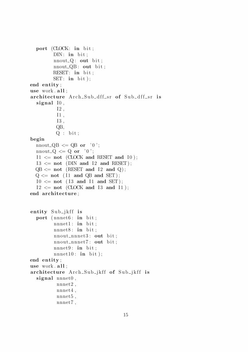
port (CLOCK: in b i t ;DIN : in b i t ;nnout Q : out b i t ;nnout QB : out b i t ;RESET: in b i t ;SET: in b i t ) ;
end entity ;use work . a l l ;architecture Arch Sub df f s r of Sub d f f s r i s
signal I0 ,I2 ,I1 ,I3 ,QB,Q : b i t ;
beginnnout QB <= QB or ’ 0 ’ ;nnout Q <= Q or ’ 0 ’ ;I1 <= not (CLOCK and RESET and I0 ) ;I3 <= not (DIN and I2 and RESET) ;QB <= not (RESET and I2 and Q) ;Q <= not ( I1 and QB and SET) ;I0 <= not ( I3 and I1 and SET) ;I2 <= not (CLOCK and I3 and I1 ) ;
end architecture ;
entity Sub jk f f i sport ( nnnet6 : in b i t ;
nnnet1 : in b i t ;nnnet8 : in b i t ;nnout nnnet3 : out b i t ;nnout nnnet7 : out b i t ;nnnet9 : in b i t ;nnnet10 : in b i t ) ;
end entity ;use work . a l l ;architecture Arch Sub jk f f of Sub jk f f i s
signal nnnet0 ,nnnet2 ,nnnet4 ,nnnet5 ,nnnet7 ,
15

nnnet3 : b i t ;begin
nnnet0 <= not nnnet1 ;nnnet2 <= nnnet3 and nnnet0 ;nnnet4 <= nnnet2 or nnnet5 ;nnnet5 <= nnnet6 and nnnet7 ;nnout nnnet7 <= nnnet7 or ’ 0 ’ ;nnout nnnet3 <= nnnet3 or ’ 0 ’ ;SUB1 : entity Sub d f f s r port map ( nnnet8 , nnnet4 , nnnet3 ,
nnnet7 , nnnet10 , nnnet9 ) ;end architecture ;
entity TestBench i send entity ;use work . a l l ;
architecture Arch TestBench of TestBench i ssignal CLEAR,
COUNT,CLOCK,Q3,Q0,Q1,Q2,nnnet0 ,nnnet1 ,nnnet2 ,nnnet3 ,nnnet4 ,nnnet5 ,nnnet6 ,nnnet7 ,nnnet8 ,nnnet9 : b i t ;
beginSUB5 : entity Sub Logic one port map ( nnnet0 ) ;nnnet1 <= Q0 and nnnet2 ;nnnet3 <= Q1 and nnnet1 ;nnnet4 <= Q2 and nnnet3 ;SUB2 : entity Sub jk f f port map ( nnnet1 , nnnet1 , nnnet5 ,
Q1 , nnnet6 , nnnet0 , nnnet7 ) ;
16
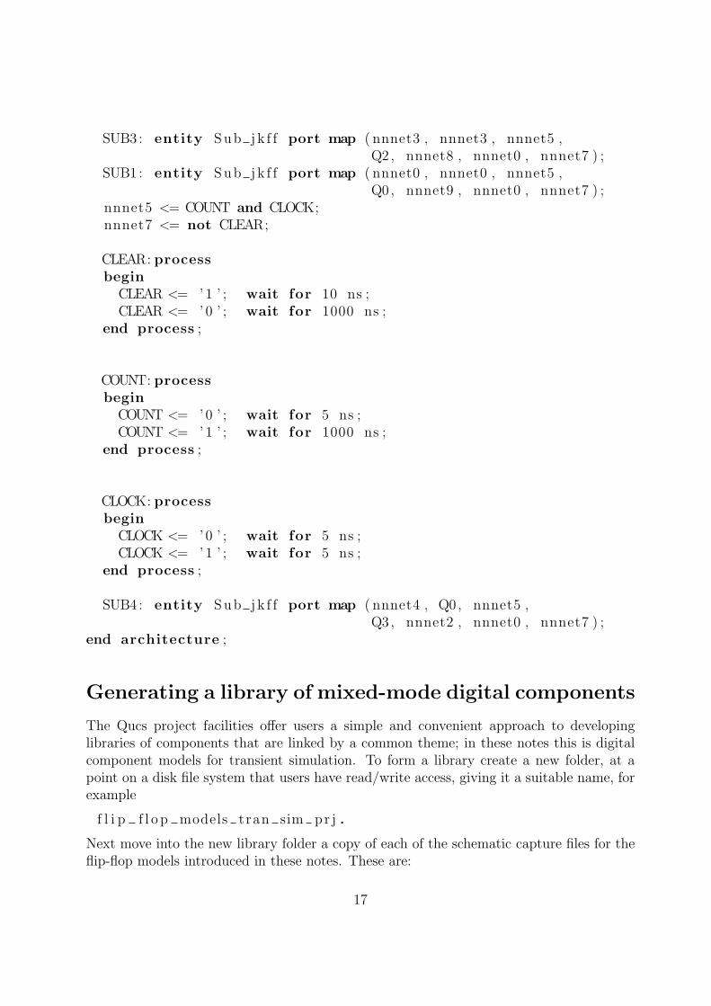
SUB3 : entity Sub jk f f port map ( nnnet3 , nnnet3 , nnnet5 ,Q2 , nnnet8 , nnnet0 , nnnet7 ) ;
SUB1 : entity Sub jk f f port map ( nnnet0 , nnnet0 , nnnet5 ,Q0 , nnnet9 , nnnet0 , nnnet7 ) ;
nnnet5 <= COUNT and CLOCK;nnnet7 <= not CLEAR;
CLEAR: processbegin
CLEAR <= ’1 ’ ; wait for 10 ns ;CLEAR <= ’0 ’ ; wait for 1000 ns ;
end process ;
COUNT: processbegin
COUNT <= ’0 ’ ; wait for 5 ns ;COUNT <= ’1 ’ ; wait for 1000 ns ;
end process ;
CLOCK: processbegin
CLOCK <= ’0 ’ ; wait for 5 ns ;CLOCK <= ’1 ’ ; wait for 5 ns ;
end process ;
SUB4 : entity Sub jk f f port map ( nnnet4 , Q0 , nnnet5 ,Q3 , nnnet2 , nnnet0 , nnnet7 ) ;
end architecture ;
Generating a library of mixed-mode digital components
The Qucs project facilities offer users a simple and convenient approach to developinglibraries of components that are linked by a common theme; in these notes this is digitalcomponent models for transient simulation. To form a library create a new folder, at apoint on a disk file system that users have read/write access, giving it a suitable name, forexample
f l i p f l o p models tran sim pr j .
Next move into the new library folder a copy of each of the schematic capture files for theflip-flop models introduced in these notes. These are:
17

d f f s r . sch , j k f f . sch , t f f . sch , and gated d l a t ch . sch .
A copy of the schematic for setting nodes to logic one is also required
( l o g i c one . sch ) .
These models are then freely available for use in any projects which users are working on.They can be copied into such projects using the ”Add files to Project...”menu button foundunder the Qucs Project drop-down menu. Similarly any new models developed as part ofa project can be added to the library and used again in the future.
Digital component propagation time delays and tran-
sient simulation numerical stability
Transient simulation is in general much slower than digital simulation using VHDL gen-erated machine code. The large signal transient simulation models of flip-flops and othersequential digital devices are intended for use in mixed-mode circuit simulation rather thanbeing used for pure digital circuit simulation. An interesting, and indeed very importantquestion, relates to the efficiency, and accuracy, of the numerical analysis algorithms em-ployed in the integration routines that are central to transient circuit simulation. Qucsallows users to select the algorithm they wish to employ for transient simulation. Theavailable algorithms are Trapezoidal, Euler, Gear and Adams Moulton; in each case thealgorithm order can be set from 1 to 6. The second order Trapezoidal integration algorithmis used by Qucs as the default for transient simulation. To test which of these algorithmsoffers the most time efficient solution to the transient simulation of digital circuits, thatinclude flip-flops, the BCD counter shown in Fig. 13 was used as a test case and repeatedlysimulated using different integration routines and algorithm orders. The test results areshown in Table 1. Very little difference was found between circuits where the cross coupledgates both had zero propagation delays and the case where one gate had 0.5ns delay andthe other zero delay.
One obvious fact emerges from the data given in Table 1; namely that the Adams Moultonhigher order integration routines appear to be faster than the default trapezoidal algorithm.This is corroborated by the average time step and number of rejection data points output
Order Trapezoidal Euler Gear Adams Moulton1 1 1.62 1.65 1.622 1 1.62 0.44 14 1 1.62 1.28 0.396 1 1.62 0.28 0.18
Table 1: Relative simulation times for the circuit shown in Fig. 13
18

Order Number or rejections Average time step1 1470 5.17737e-122 1750 9.4585e-124 1454 2.866e-116 61 5.76646e-11
Table 2: Number of rejections and average time step data for the Adams Moulton algorithm
by Qucs at the end of a simulation. Table 2 lists this data for the Adams Moulton algorithmtabulated in Table 1.
Table 2 points to the increase in average time step and the dramatic reduction in the num-ber of simulation solution rejections as the probable reason for the reduction in transientsimulation time when using the higher order Adams Moulton integration routines. How-ever, other factors may influence the choice of integration routine. Often speed is not theonly criteria that is of importance when simulating large complex circuits. Consider thefollowing case (the circuit shown in Fig. 13 with order 6 Adams Moulton transient analysisintegration); setting one of the gate delays to 1ns, and the other to 0ns, in each of the RSlatches in the edge-triggered D flip-flop yields the signal waveforms illustrated in Fig. 18.Clearly here the solution is incorrect pointing to probable numerical instability caused bythe choice of integration routine.
0 1e-8 2e-8 3e-8 4e-8 5e-8 6e-8 7e-8 8e-8 9e-8 1e-7 1.1e-7 1.2e-70
1
time
CLE
AR
.Vt
0 1e-8 2e-8 3e-8 4e-8 5e-8 6e-8 7e-8 8e-8 9e-8 1e-7 1.1e-7 1.2e-70
1
time
CLO
CK
.Vt
0 1e-8 2e-8 3e-8 4e-8 5e-8 6e-8 7e-8 8e-8 9e-8 1e-7 1.1e-7 1.2e-7
0
1
time
Q0.
Vt
0 1e-8 2e-8 3e-8 4e-8 5e-8 6e-8 7e-8 8e-8 9e-8 1e-7 1.1e-7 1.2e-70
1
time
CO
UN
T.V
t
0 1e-8 2e-8 3e-8 4e-8 5e-8 6e-8 7e-8 8e-8 9e-8 1e-7 1.1e-7 1.2e-7
0
1
time
Q1.
Vt
0 1e-8 2e-8 3e-8 4e-8 5e-8 6e-8 7e-8 8e-8 9e-8 1e-7 1.1e-7 1.2e-7
0
1
time
Q2.
Vt
0 1e-8 2e-8 3e-8 4e-8 5e-8 6e-8 7e-8 8e-8 9e-8 1e-7 1.1e-7 1.2e-7
0
1
time
Q3.
Vt
Figure 18: Digital TimeList waveforms for the circuit shown in Fig. 13
19

Mixed-mode example simulations
Mixed-mode simulation involves the simulation of circuits that contain electronic devicesand circuits from different physical domains; the most obvious being circuits with a mixtureof analogue and digital components. Qucs has developed to a point where it can handle thistype of circuit given device models that can span across the different physical domains. Inthe future such circuits are likely to incorporate components from other domains, includingfor example, digital signal processing components (DSP) and possibly nano mechanicaldevices. Multi-domain simulation adds additional complexity to the simulation processnot normally found in single domain simulation. Each domain usually represents signaldata in a specific way attributed to a given domain; voltage and current for analoguequantities, boolean ’1’ and ’0’ for digital signals and floating point numbers for DSP.Hence, signals passing from one domain to another have to be converted from one formatto another. These conversion elements are often called node-bridges and form an essentialpart of the mixed-mode simulation process. The three examples that are introduced in thissection of these notes have been chosen to illustrate a number of the basic ideas concernedwith mixed-mode simulation of circuits containing analogue and digital components, andto show how Qucs deals with this type of simulation. In the last section the importanceof correct selection of integration routine when simulating circuits in the time domain wasstressed. Mixed-mode circuits often include a wide diversity of components that exhibitwidely differing time constants. This makes the problem of numerical stability versussimulation run time even more critical. With the explicit numerical integration routines,like the trapezoidal routine, numerical instability results if the simulation time step becomesmuch larger than the smallest time constant in a circuit. Hence, to achieve successfulcompletion of a simulation the integration time step must be reduced which in turn makesthe overall simulation time increase significantly. The implicit Gear algorithm5 does notsuffer from this problem and is the natural choice for circuits with components that havewidely differing time constants.
• Example 1: Analogue waveform driven digital devices with output node-bridge.
The circuit in Fig. 19 shows an analogue voltage source driving a digital inverterwith a node-bridge element processing the inverter output signal. The input signalis a sinusoidal voltage of amplitude 1V peak. The inverter output signal, V1 inFig. 19, has an nonsymmetrical mark to space ratio because the threshold point forthe inverter is set at 0.5V; the halfway point for the two logic levels. The node-bridgeelement is basically a voltage controlled voltage source where the device gain and timedelay can be programmed. In this first example the gain has been set to 5 and thetime delay to 0.5ns. Figure 20 illustrates the simulation TimeList waveforms for thisexample mixed-mode circuit. The node-bridge shown in Fig. 19 is a very basic device.Moreover, by adding additional features, parameters like fall and rise time can set tospecific values. The next example demonstrates the use of an active node-bridge.
5The Gear integration algorithm is a powerful method for solving stiff systems of differential equations,see Donald A. Calahan, Computer Aided Network Design, Revised edition, 1972, McGraw-Hill.
20

1
Y1
V1U=1 V
transientsimulation
TR1Type=linStart=0Stop=20usIntegrationMethod=GearOrder=6
D to ANodeBridge
VINN
VINP VOUTP
VOUTN
SUB1File=a_node_bridge.sch
Vin V1 V5D
Figure 19: Analogue waveform driven digital device with output node-bridge
0 2e-6 4e-6 6e-6 8e-6 1e-5 1.2e-5 1.4e-5 1.6e-5 1.8e-5 2e-5
0
time
Vin
.Vt
0 2e-6 4e-6 6e-6 8e-6 1e-5 1.2e-5 1.4e-5 1.6e-5 1.8e-5 2e-50
5
time
V5D
.Vt
0 2e-6 4e-6 6e-6 8e-6 1e-5 1.2e-5 1.4e-5 1.6e-5 1.8e-5 2e-5
0
1
time
V1.
Vt
Figure 20: Digital TimeList waveforms for the circuit shown in Fig. 19
21

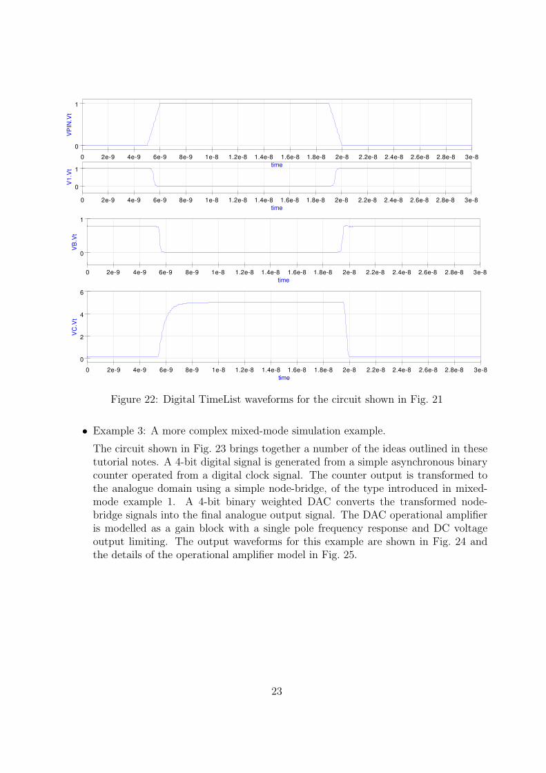
• Example 2: Pulse driven digital inverter with an active node bridge.
Illustrated in Fig. 21 is a similar circuit to the previous example. In Fig. 21 apulse generator drives a digital inverter. The inverter output signal is processed byan active node-bridge derived from a basic BJT switching amplifier. The outputwaveforms for this circuit are shown in Fig. 22. Notice that the pulse rise and falltimes are determined by the node-bridge amplifier and that the resulting analoguesignal amplitude is set to 5V.
1
Y1
T1Type=npnIs=1e-16Nf=1Vaf=0Bf=100
R1R=10k Ohm
C1C=0.1 pF
V3U1=0 VU2=1 VT1=5nsT2=20ns
R2R=4.7 k Ohm
V2U=5 V
transientsimulation
TR1Type=linStart=0Stop=30nsIntegrationMethod=GearOrder=6
V1VPIN
VC
VB
Figure 21: Pulse driven digital inverter with active node-bridge
22
0 2e-9 4e-9 6e-9 8e-9 1e-8 1.2e-8 1.4e-8 1.6e-8 1.8e-8 2e-8 2.2e-8 2.4e-8 2.6e-8 2.8e-8 3e-8
0
1
time
V1.
Vt
0 2e-9 4e-9 6e-9 8e-9 1e-8 1.2e-8 1.4e-8 1.6e-8 1.8e-8 2e-8 2.2e-8 2.4e-8 2.6e-8 2.8e-8 3e-8
0
1
time
VP
IN.V
t
0 2e-9 4e-9 6e-9 8e-9 1e-8 1.2e-8 1.4e-8 1.6e-8 1.8e-8 2e-8 2.2e-8 2.4e-8 2.6e-8 2.8e-8 3e-8
0
1
time
VB
.Vt
0 2e-9 4e-9 6e-9 8e-9 1e-8 1.2e-8 1.4e-8 1.6e-8 1.8e-8 2e-8 2.2e-8 2.4e-8 2.6e-8 2.8e-8 3e-8
0
2
4
6
time
VC
.Vt
Figure 22: Digital TimeList waveforms for the circuit shown in Fig. 21
• Example 3: A more complex mixed-mode simulation example.
The circuit shown in Fig. 23 brings together a number of the ideas outlined in thesetutorial notes. A 4-bit digital signal is generated from a simple asynchronous binarycounter operated from a digital clock signal. The counter output is transformed tothe analogue domain using a simple node-bridge, of the type introduced in mixed-mode example 1. A 4-bit binary weighted DAC converts the transformed node-bridge signals into the final analogue output signal. The DAC operational amplifieris modelled as a gain block with a single pole frequency response and DC voltageoutput limiting. The output waveforms for this example are shown in Fig. 24 andthe details of the operational amplifier model in Fig. 25.
23

Q
R
Q
STSUB5
File=tff.sch
Q
R
Q
STSUB6
File=tff.sch
Q
R
Q
STSUB7
File=tff.sch
1SUB9File=Logic_one.sch
S1Num=1
S2Num=2
D to ANodeBridge
VINN
VINP VOUTP
VOUTN
SUB10File=a_node_bridge.sch
D to ANodeBridge
VINN
VINP VOUTP
VOUTN
SUB11File=a_node_bridge.sch
R10R=5k Ohm
D to ANodeBridge
VINN
VINP VOUTP
VOUTN
SUB12File=a_node_bridge.sch
R4R=2.5k
R2R=10k Ohm
+V+
V-
SUB14File=spole_op_amp.sch
V1U=18 V
transientsimulation
TR1Type=linStart=0Stop=40 mIntegrationMethod=GearOrder=6
V2U=18 V
Q
R
Q
STSUB8
File=tff.sch
D to ANodeBridge
VINN
VINP VOUTP
VOUTN
SUB13File=a_node_bridge.sch
R5R=1.25k Ohm
R1R=10k Ohm
CLOCK
B0
B1
B2
A_VOUT
B3
RESET
Figure 23: A more complex analogue-digital mixed-mode simulation example
24

0 0.002 0.004 0.006 0.008 0.01 0.012 0.014 0.016 0.018 0.02 0.022 0.024 0.026 0.028 0.03 0.032 0.034 0.036 0.038 0.040
1
time
RE
SE
T.V
t
0 0.002 0.004 0.006 0.008 0.01 0.012 0.014 0.016 0.018 0.02 0.022 0.024 0.026 0.028 0.03 0.032 0.034 0.036 0.038 0.04
0
1
time
B0.
Vt
0 0.002 0.004 0.006 0.008 0.01 0.012 0.014 0.016 0.018 0.02 0.022 0.024 0.026 0.028 0.03 0.032 0.034 0.036 0.038 0.04
0
1
time
B1.
Vt
0 0.002 0.004 0.006 0.008 0.01 0.012 0.014 0.016 0.018 0.02 0.022 0.024 0.026 0.028 0.03 0.032 0.034 0.036 0.038 0.04
0
1
time
B2.
Vt
0 0.002 0.004 0.006 0.008 0.01 0.012 0.014 0.016 0.018 0.02 0.022 0.024 0.026 0.028 0.03 0.032 0.034 0.036 0.038 0.040
1
time
CLO
CK
.Vt
0 0.002 0.004 0.006 0.008 0.01 0.012 0.014 0.016 0.018 0.02 0.022 0.024 0.026 0.028 0.03 0.032 0.034 0.036 0.038 0.04-20
0
time
A_V
OU
T.V
t
0 0.002 0.004 0.006 0.008 0.01 0.012 0.014 0.016 0.018 0.02 0.022 0.024 0.026 0.028 0.03 0.032 0.034 0.036 0.038 0.04
0
1
time
B3.
Vt
Figure 24: Digital TimeList waveforms for the circuit shown in Fig. 23
25

VINPNum=1
VINNNum=2
R1R=200k Ohm
VOUTNum=3
R3R=50 Ohm
SRC1G=1T=0
SRC2G=200kT=0
R4R=10k Ohm
C1C=3.2uF
D1Is=1e-15 AN=1Cj0=10 fFM=0.5Vj=0.7 V R5
R=5 Ohm
D2Is=1e-15 AN=1Cj0=10 fFM=0.5Vj=0.7 V
R6R=5 Ohm
VDCPNum=4
VDCNNum=5
Figure 25: Operational amplifier model with Rin = 200k Ω, pole frequency = 5Hz, DCdifferential gain = 200k and Rout = 50 Ω
26

End Note
The examples described in these notes were all simulated using the latest CVS code versionof Qucs. Since release of version 0.0.8, Qucs has matured enough to allow it to be used formixed-mode simulation and many of the known bugs in Qucs 0.0.8 will be corrected with therelease of Qucs 0.0.9 some time in the future. Release 0.0.9 will represent another importantstep in the development of a truly universal simulator. However, much more work needs tobe done on the development of models for use across the different physical domains. Mythanks to Michael Margraf and Stefan Jahn for all their hard work in correcting the bugswhich surfaced while the examples presented in this tutorial note where being tested.
27