quantum transport in graphene -...
TRANSCRIPT

ChunChun Ning Lau Ning Lau (Jeanie)(Jeanie)
Quantum TransportQuantum Transportinin
Graphene Graphene

April 11, 2008 SSSC Meeting
Acknowledgement
Ulas Coskun
Feng Miao
Jairo VelascoGang Liu
Sitara Wijeratne
Wenzhong Bao
Yong Zhang
Graduate Students (Former) Postdocs
Undergraduate Students
Discussion WithShan-Wan Tsai, Marc Bockrath,Antonio Castro-Neto, Michale Fogler,Gil Refael, Dmitri Abanin, Philip Kim,Chandra Varma, Leonid Pryadko,Dmitry Novikov, Alex Bratkosvki

April 11, 2008 SSSC Meeting
• Rise of Graphene
• Overview of recent experimental progresses
• Minimum conductivity
• Quantum interference of charges
• Supercurrent Transistors
• Quantum Hall states in p-n junctions
• Conclusion and outlook
Outline

April 11, 2008 SSSC Meeting
Scale of Things1 mm10-3 m
Micro-Electro-Mechanical devices
48 iron atoms on copper
Humanhair
Carbonnanotubes
0.1 nm
1 nm
10 nm
0.1 µm100 nm
1 µm
10 µm
0.1 mm100 µm
10-4 m
10-5 m
10-6 m
10-7 m
10-8 m
10-9 m
10-10 m
Micro-electronicsMicro-electronics
Bloodcells
E. ColiBacteria Nnanowires
Graphene
Self-assembled Human-assembled
SemiconductorHeterostructures• quantum dots• quantum wires• 2DEG

April 11, 2008 SSSC Meeting
0D, 1D, 2D and 3D Carbon
0D 1D 2D 3D
Discovered 1985 1991, 1993 2004 Images taken from scifun.ac.uk
From Novoselov’s presentation at IWCNM,Kirchberg, 2007
April 11, 2008 SSSC Meeting
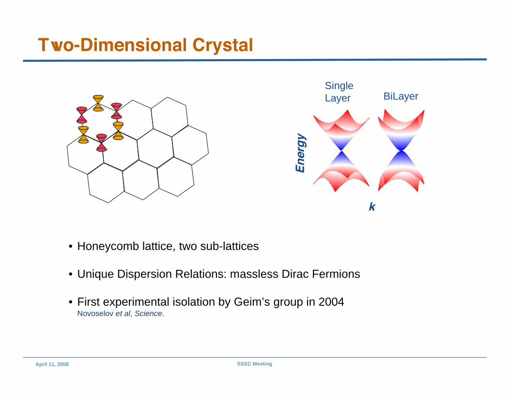
Two-Dimensional Crystal
SingleLayer
k
Ener
gy
BiLayer
• Honeycomb lattice, two sub-lattices
• Unique Dispersion Relations: massless Dirac Fermions
• First experimental isolation by Geim’s group in 2004 Novoselov et al, Science.

April 11, 2008 SSSC Meeting
Half-integer Quantum Hall EffectGraphene
• New model system for condensed matter researchVeselago lensing, Klein tunneling, Spin transport, Supercurrent transistor…
• Surface 2DEG•Optical, STM and mechanical measurements•Easily coupled to special electrodes (superconductors, ferromagnets)
Novoselov et al Nature 2005;Zhang et al, Nature 2005.
Semiconductors
!
EN
= ±vF2ehBN
!
EN
= ±heB
mN + 1
2( )
!
" xy = ±4e
2
hN + 1
2( )
LandauLevels

April 11, 2008 SSSC Meeting
Optical ProbesARPES probe of Electronic structures
Zhou et al, NaturePhysics (2006)Bostwick et al, NaturePhysics (2007)
Raman spectroscopy
•Identify number of layer•Study electron-phonon dynamics•Measure thermal conductivity
Ferrari et al, PRL (2006).Yan et al, PRL (2007).Pisana et al, Nature Mat.(2007)Balandin et al, Nano Lett.(2008)
Raman shifts
Optical absorbance ~ (# layers)
!
"e2
hc
Optical Transmission & Conductivity
Nair et al, cond/mat (2008)
See also Kuzmenko et al, PRL(2008) for multilayer graphiteWang et al,
Science(2008)
Gate-Variable IR Transitions

April 11, 2008 SSSC Meeting
Mechanical Properties
• Single Atomic Layer Mechanical Resonator
Bunch et al, Science (2007)
• Ripples in Suspended Graphene
Meyer et al, Nature (2007)
• Measured Young’s modulus 0.5TPa• Spring constant 1-5 N/m
Frank et al, J. Vac. Sci. Technol. B (2007)

April 11, 2008 SSSC Meeting
Applications
Post-silicon electronic material
• With advantages of carbon nanotubeshigh thermal conductivity (5000 W/mK)high current density (~ mA/µm width)high mobility (~10,000 V/cm-s in as-prepared samples)
• 2D → compatible with lithographic techniques
• Potential for large scale synthesis
Epitaxially grown grapheneBerger et al, Science (2006)

April 11, 2008 SSSC Meeting
Graphene Field-Effect Transistors
• Graphene Nano-ribbon FET• Band induced by quantum confinement
!
Eg "0.2
W #W *
eV
nm
Han et al, PRL (2007)Chen et al, Physica E (2007)
Li et al, Science (2008)Wang et al, cond/mat (2008)
•Chemically derived nanoribbons•Almost all semi-conducting•On/off ratio ~106, mobility ~200 cm2/Vs
•Lithographically defined nanoribbons

April 11, 2008 SSSC Meeting
• Post-silicon electronic material
• With advantages of carbon nanotubeshigh thermal conductivity (5000 W/mK)high current density (~ mA/µm width)high mobility (~10,000 V/cm-s in as-preparedsamples)
• 2D → compatible with lithographic techniques
• Transparent electrodes for solar cells, LCD, etc
• Chemical and biological sensors based ongraphene
• Electronics, Spintronics, and Valley-tronics
Applications
Ultra-sensitive gas sensorsSchedin et al, Nature Materials (2006).
Blake et al, cond/mat (2008)

April 11, 2008 SSSC Meeting
The Band…
k
Ener
gy

April 11, 2008 SSSC Meeting
The Bandwagon!
400
300
200
100Num
ber
of P
aper
s
20072006200520042003Year
Number of papers on arXivwith keyword graphene

April 11, 2008 SSSC Meeting
• Rise of Graphene
• Overview of recent experimental progresses
• Minimum conductivity• Quantum interference of charges• Supercurrent Transistors
• Quantum Hall states in p-n junctions
• Conclusion and outlook
Outline

April 11, 2008 SSSC Meeting
Extraction of Single- and Bi-Layer Graphene
• Mechanical exfoliation -- rub natural graphite flakes onto SiO2 substrate
• Identify the number of layers by color contrast in optical microscopes(other methods: Raman and transport)
• AFM images reveal mesoscopic features
Single-layer graphene Bi-layer graphene
2µm2µm
SL
Multiple
150°
5 µm 1-layer
2-layer
3-layer
AFMOptical Microscope

April 11, 2008 SSSC Meeting
Two steps of E-beam lithography• Alignment Marks• Electrodes (3-10 nm Ti or Pd + 70 nm Al)
Single-layer graphene device
Device Fabrication
6µm
Bi-layer graphene device
300nm
Vg

April 11, 2008 SSSC Meeting
Half Integer Quantum Hall Effect
Conductivity of single layer graphene quantized at half-integral valuesof 4e2/h
–> confirmed selection of single layer graphene
5.54.53.52.51.50.5
-0.5-1.5-2.5-3.5
!xy
(4e2 /h
)
6040200-20-40Vg (V)
Measurement performed at B=8T and T=260mK

April 11, 2008 SSSC Meeting
• Graphene as bipolar field-effect transistors– Conductivity increases linearly with charge density n
– σ remains finite at Dirac point → σmin
• Theoretical prediction: universal value of GQ=4e2/πh– independent of vF,– for both ballistic and disordered regimes.
Fradkin 1986; Lee 1983; Peres et al (2006), Nilsson et al (2006), Katsnelson (2006),Tworzydlo et al (2006)…..
• Experimental measurements: 4e2/h, π times larger thantheory (Novoselov et al, Nature, 2005.)→the mystery of missing π
• What limits mobility?
Minimum Conductivity Controversy
hole-doped
electron-doped
Dirac Pt!
" #Vg # n

April 11, 2008 SSSC Meeting
Our Findings
Devices with large source-drain separation (> 1µm) and large areas (>0.3 µm2)• σmin ~ 4e2/h• σ linear in gate voltage• mobility µ=8000 - 15000 cm2/Vs
→ Fully consistent with results in Novoselov et al, Nature, 2005.
3
2
1
G (
mS
)
30V10Vg (V)
5µm
T=1.5 K
200nm

April 11, 2008 SSSC Meeting
• Minimum conductivity ranges from 0.8 to 4.3 (4e2/πh)
• G-Vg frequently displays sub-linear relationship
800
600
400
200
G (µ
S)
-40 -20 0 20 40Vg (V)
1500
1000
500-100 -50 0
Bi-layer
Single-layer
Our Findings
Devices with small source-drain separation (< 400 nm) and small areas (<0.1 µm2)
T=1.5 K
300nm
WL

April 11, 2008 SSSC Meeting
4
2
0!
min
(4e
2/"
h)
1086420Aspect Ratio W/L
What’s Going On???
• σmin depends on devices’ aspect ratio W/L for a ballistic transport in graphene– At Dirac point, transmission via evanescent modes– Use Landauer formula– Only approaches 4e2/πh for W/L >>1
!
"min =Gmin
L
W=2e
2
h
L
WTn
n=#(N#1)
N#1
$!
Tn
=1
cosh2("nL /W )
Tworzydlo et al, PRL, 2006:
Good agreement with data.
4
2
0!
min
(4e
2/"
h)
1086420Aspect Ratio W/L

April 11, 2008 SSSC Meeting
Minimum Conductivity
5
0840
Small Devices Large Devices
• Transition from ballistic transport to quasi-diffusive regimes
• charge transport is ballistic up to ~ 500 nm
• Possible mechanisms of transition- inhomogeneous doping; long range Coulomb scatterers
4
2
0
!m
in (
4e
2/"
h)
1086420Aspect Ratio W/L

April 11, 2008 SSSC Meeting
What Limits Mobility?
• Charge inhomogenity, atomic defects,rough edges
• Contaminants– Thermal and chemical annealing– Current annealing
(Bachtold group, Fuhrer group)
• Substrate– Use different substrates– Free-standing graphene
(Kim group, Andrei group, cond/mat 2008)
• Ripples -- intrinsic!– Apply tension?
Martin et al, Nature Physics (2008)
Spatial variation of charge density
April 11, 2008 SSSC Meeting
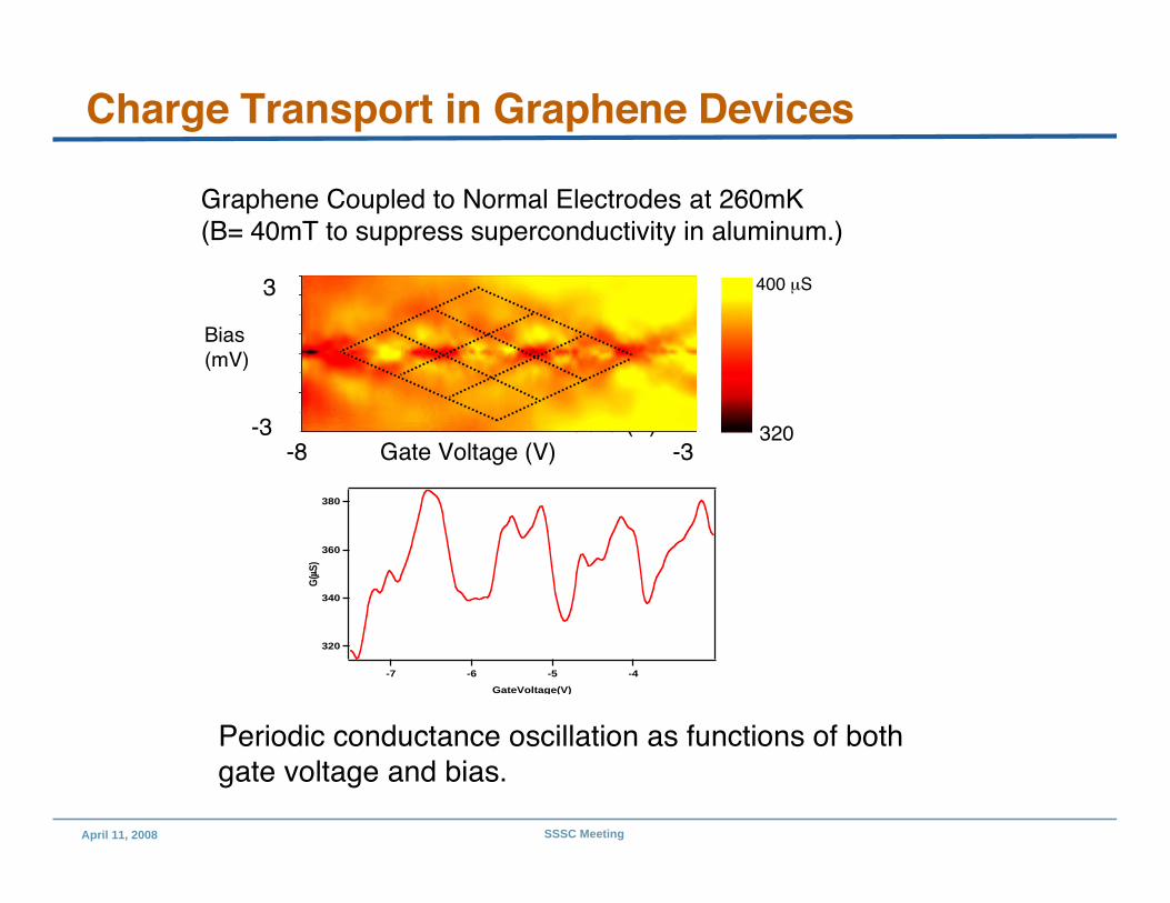
Charge Transport in Graphene Devices
Graphene Coupled to Normal Electrodes at 260mK(B= 40mT to suppress superconductivity in aluminum.)
400 µS
320Gate (V)
Bias(mV)
-8 -3-3
3
Gate Voltage (V)
380
360
340
320
G(µ
S)
-7 -6 -5 -4
GateVoltage(V)
Periodic conductance oscillation as functions of bothgate voltage and bias.

April 11, 2008 SSSC Meeting
Charge Transport in Graphene Devices
• Robust phenomena -- observed for both single and bi-layer devices, andfor both hole- and electron-doped regimes.
270
320

April 11, 2008 SSSC Meeting
•Similar conductance oscillation observed in carbon nanotubes
•Fabry-Perot resonant cavity -- interference of multiply-reflected electronand hole waves between partially transmitting electrodes.
Quantum Interference of Electron Waves in Graphene
Carbon Nanotubes
ElectrodeElectrodeGraphene

April 11, 2008 SSSC Meeting
Graphene as a Quantum Billiard
• Typically more than 1 period was observed in graphene devices• Characteristic energy scale Eo = hvF/2L
– Nanotubes: L ~ inter-electrode spacing for nanotubes– Graphene: L ~ ?
• Electron paths in 2D graphene are not well-defined as in 1D nanotubes• Smallest Eo ~ 0.7 meV → Charge coherence length ~3- 5 µm in graphene
GrapheneNanotubes
Liang et al,Nature (2001).
F. Miao, S. Wijeratne, Y. Zhang, U. C. Coskun, W. Bao, C. N. Lau, Science, 2007.

April 11, 2008 SSSC Meeting
• Rise of Graphene
• Overview of recent experimental progresses
• Minimum conductivity
• Quantum interference of charges
• Supercurrent Transistors• Quantum Hall states in p-n junctions
• Conclusion and outlook
Outline

April 11, 2008 SSSC Meeting
Graphene Coupled to Superconducting Electrodes
New phenomena expected:•Specular Andreev reflection (Beenakker, PRL 2006, Titov and Beenakker, PRB 2006)
•Novel propagating modes of Andreev electrons (Titov, Ossipov and Beenakker, 2006)
•Oscillation of tunneling probability with barrier width (Sengupta 2006)
…
Josephson junction with 2D massless Dirac fermions10 nm Pd+ 70 nm Al
SC SC
Weak link
Is= Ic sin (ϕ1−ϕ2)

April 11, 2008 SSSC Meeting
Graphene Supercurrent Transistor
-50
0
50
V(µ
V)
-80 -40 0 40 80I(nA)
Vg
-80
-40
0
40
80
I(nA
)
-40 -20 0 20 40Gate Voltage (V)
-50
0
50V(µV)
•Supercurrent in graphene first reported by Heersche et al, Nature, 2007 and Du et al, cond/mat, 2007.
•V-I characteristics tuned by gate voltages
Single Layer Graphene Device with Ti (5nm)/ Al (80 nm) electrodes.

April 11, 2008 SSSC Meeting
Graphene Supercurrent Transistor
•Supercurrent carried by electrons, holes and in nominally undoped regimes.
•Critical current depends on gate voltage.
50
0
-50
V (µ
V)
4002000-200-400I (nA)
Vg
Ic
V(µV)

April 11, 2008 SSSC Meeting
Ic and IcRN Product
Regular Josephson Junction
• tunnel or diffusive SNS junction:Ic ~ 2Δ/RN
• ballistic single channel junction:Ic~ 2πeΔ/hIcRN ~ 2Δ/e
• Ic and IcRN product are typicallyconstant for a given device
Titov and Beenakker (2006)
Graphene Josephson Junctionin the ballistic limit
change with Vg
!
Ic"e#
h
W
L
IcRN~ 2# /e

April 11, 2008 SSSC Meeting
Experimental Measurements of IcRN
Titov and Beenakker (2006)
•Ic,expt < Ic, theory and IcRN, expt < IcRN, theory
by a factor of 5-10• thermal fluctuation(?)
•Large variation in IcRN product•Similar observation reported by Heersche et al.
Heersche et al, Nature, 2007
30
20
10
I c(nA
)
-40 -20 0 20Vg (V)
10
8
6
I cRN
(µV)
-40 -20 0 20Vg (V)

April 11, 2008 SSSC Meeting
Dissipation in Josephson Junctions
Dissipation ~ 1/hysteresis– Underdamped Josephson junction with
premature switching– Dissipation changes with gate voltage
Phase across junction ⇔ particle in a titled washboard potential
Dissipation ⇔ friction ~ 1/RN
Superconducting state ⇔ localized particle
Normal state ⇔ particle running down the potential
R
C
JJ
Resistively and Capacitively Shunted Junction
-30
-20
-10
0
10
20
30
V (µ
V)
-100 -50 0 50 100I (nA)

April 11, 2008 SSSC Meeting
Evidence for Gate Tunable Dissipation
3.5
3.0
2.5
2.0
1.5
1.0
Nor
mal
ized
I cR
N
-40 -20 0 20Vg (V)
Calculation Data
2.5
2.0
1.5
I cRN
(µV)
-40 -20 0 20Vg (V)
• Qualitatively account for the large variation in IcRN• Role of massless Dirac Fermions?

April 11, 2008 SSSC Meeting
• Rise of Graphene
• Overview of recent experimental progresses
• Minimum conductivity
• Quantum interference of charges
• Supercurrent Transistors
• Quantum Hall states in p-n junctions• Conclusion and outlook
Outline

April 11, 2008 SSSC Meeting
Graphene p-n Junctions
• Unique advantage: local control of charge density and type
• Graphene p-n junctions with top gate(s):•allow in situ tuning of junction polarity and dopant levels•Partial equilibration of quantum hall edge states
• Application• Band gap engineering of bi-layer graphene• Veselago lensing (optics-like focusing of electron rays)• Particle collimation• Valley polarization
Topgate
Graphene
V A
Vg
Theories: Abanin et al 2006, 2007; Fogler et al 2007; Shytov et al 2007; Katsnelson et al 2006; Beenakker group,Cheianov et al 2006, 2007
Experimental demonstration: Huard et al 2007; Williams et al 2007, Ozyilmaz et al 2007, Oostinga et al 2007

April 11, 2008 SSSC Meeting
Graphene p-n Junctions• Challenge: deposition of top gate tends to dope or damage the atomic layer• Innovation: Suspended, contactless top gate
•Gentle process•Graphene can be annealed
• Quantum Hall conductance plateau at fractional values of e2/h
ElectrodeGraphene
Suspended gate
Topgate
Graphene
V A
Vg
Topgate
Graphene
V A
Vg

April 11, 2008 SSSC Meeting
Quantum Hall States in graphene p-n Junctions
• Fractional quantum Hall plateau observed• Edge state equilibration, full mixing of propagation modes at interface
Marcus group, Science,August 2007.
p p’
np
!
G =e2
h
"1"2
"1
+ "2
!
G =e2
hmin "1 ," 2( )
2 resistors in series
Abanin & Levitov, Science, 2007

April 11, 2008 SSSC Meeting
Quantum Hall States in graphene p-n-p Junctions
• Fractional quantum Hall plateau observed• Edge state equilibration, full mixing of propagation modes at interface
Observation of 2e2/h plateau --> small amount of disorder
Top Gate
p n p
Ozyilmaz et al 2007
B=8T
2.0
1.5
1.0
G (e
2 /h)
200Vtg (V)
6/5
2/3
R(kΩ)
pnpp
B=0T
G(e2/h)
Liu, Velasco Jr. and Lau, submitted (2007)

April 11, 2008 SSSC Meeting
On-going Collaborations
• Spin transport (with Kawakami at UCR)
• Thermopower (with Shi at UCR)
• Thermal conductivity (with Dames at UCR)
• STM (with Yeh at Caltech, LeRoy at U. Arizona)
• Photoconductivity (with Kalugin at New Mexico Tech)
• Raman spectroscopy (with Alex Balandin at EE, UCR)
• Graphene as an electronic material (with Bockrath at Caltech)

April 11, 2008 SSSC Meeting
Challenges and PromisesGraphene is a fascinating platform for investigating 2D, relativisticand/or many-body physics
•Many novel phenomena predicted•More surprises ahead
→Specular Andreev reflection→Valley control→Spin manipulation→Fractional quantum Hall effect(?)→Bilayer Dirac fermion quantum Hall systems→Veselago lensing…
•Material optimization to improve mobility
•Precision control of crystallographic edges

April 11, 2008 SSSC Meeting
Challenges for Technological Applications
3.Band Gap engineering• nanoribbon• chemical modification• strain• local gates
2. Precision crystallographic edge control• Chemical modification

April 11, 2008 SSSC Meeting
Graphene for Sale
Flake sizesLargest monolayer found to date: 7000 µm2, but typically < 600 µm2
Pricing guide≈ £ 0.50 -- 2 per µm2 areaApplicationstransistors, spintronics, gas sensors, metrology, Ramanspectroscopy, AFM, STM, etc.
1 µm2 contains 3 x 10⁷ atoms1g contains 5 x 10 22 atoms1 £ ~ 2 US $
Cost per gram: ~ US $ 1015
US National Debt ~ $ 9 x 10 12
Do you take payment in graphene?
Available in 10 mg or a 10 m2 roll.

April 11, 2008 SSSC Meeting
Challenges for Technological Applications
1.Large Scale Synthesis & Production•wafer-scale•high mobility•precision control of number of layers.
•CVD epitaxial growth:– Thermally remove Si from SiC substrate– Grow graphene on BN substrates
•Chemical method– Reduction of graphite oxide– Intercalation and exfoliation of bulk graphite

April 11, 2008 SSSC Meeting
The bandwagon in 10 years
?

April 11, 2008 SSSC Meeting
The bandwagon in 10 years
Science
Technology

April 11, 2008 SSSC Meeting
Thank You!