quantum light-matter interactions in solids: towards...
TRANSCRIPT

7–8 September 2017 Institute of Physics, London, UK
Quantum Light-Matter Interactions in Solids: towards integrated
quantum photonics
Programme and Abstract Book

1
Thursday 7 September 2017
09:40 Registration and coffee
10:20 Welcome and opening remarks (Franklin Lecture Theatre)
10:30 (invited) Towards an integrated quantum photonics platform on GaAs Sven Hoefling, St Andrews University, UK and Würzburg University, Germany
11:00 Refreshment break
11:20 Integrating multiple LEDs on a substrate to create electrically driven and tuneable quantum light sources Anthony Bennett, Toshiba Research Europe Limited, UK
11:40 (invited) Photonic trumpets for quantum optics and hybrid optomechanics Jean-Michel Gerard, CEA/INAC, France
12:10 Progress on optical fabrication and characterisation of SU-8 disc modulated mode-gap photonic crystal cavities Stephen Lennon, University of Oxford, UK
12:30 Lunch
14:00 (invited) Intrinsic phonon scattering limitations of on-demand quantum dot single-photon sources Stephen Hughes, Queen's University, Canada
14:30 Circumventing phonon effects in optical state preparation of quantum dots using adiabatic rapid passage Doris Reiter, Westfälische Wilhelm-Universität Münster, Germany
14:50 Quantum light-matter interaction at on-chip temperature conditions with a-plane InGaN quantum dots Tong Wang, University of Oxford, UK
15:10 Coffee break
16:10 On-chip electro-mechanical routing of single photons from an embedded quantum emitter Zofia Bishop, University of Sheffield, UK
16:30 Efficient classical algorithm for boson sampling with partially distinguishable photons Jelmer Renema, University of Oxford, UK
16:50 Welcome reception

Friday 8 September 2017
09:30 Registration and coffee
10:00 (invited) Solid state quantum optics on a chip Maurice Skolnick, University of Sheffield, UK
10:30 Highly polarized electrically driven single photon emission from a non-polar InGaN quantum dot Claudius Kocher, University of Oxford, UK
10:50 (invited) Cavity QED with carbon nanotubes Philippe Roussignol, Ecole Normale Supérieure, France
11:20 Refreshment break
11:40 Effect of excitation conditions on the purity of quantum emission from InGaN Helen Springbett, University of Cambridge, UK and The University of Tokyo, Japan
12:00 Optical properties of topological insulator nanoparticles Gleb Siroki, Imperial College London, UK
12:20 Multimode polariton solitons in microcavity wires for polaritonic integrated circuits Gaby Slavcheva, University of Bath, UK and Johannes Kepler University Linz, Austria
12:40 Lunch
14:00 High principal quantum number excitons in cuprous oxide semiconductor crystal Joshua Rogers, University of Durham, UK
14:20 Photonic waveguides for 780 nm optical delivery for quantum sensors based on ultra-cold atoms of Rubidium Jessica Maclean, University of Nottingham, UK
14:40 Closing remarks
15:00 Conference closes

3
(invited) Towards an integrated quantum photonics platform on GaAs
S Höfling1,2, C P Dietrich1, A Fiore3, M Thompson4 and M Kamp1 1Universität Würzburg, Germany 2University of St Andrews, UK, 3Eindhoven University of Technology, The Netherlands 4University of Bristol, UK
Quantum information processing is a rapidly developing research field. The exploitation of quantum bits instead of classical bits offers key advantages for future technologies including secure communication and ultra-fast computation. Lab-size experiments on quantum information processes have already proven the validity of its concepts. However, any wide spread utilization will require dense integration of functionalities. This requires the realization of semiconductor integrated quantum photonic circuits on a single- semiconductor chip with embedded sources, photon processing units and detectors on the single photon level. Among the different material platforms currently being investigated, direct-bandgap semiconductors and particularly gallium arsenide (GaAs) offer the widest range of functionalities, including single and entangled-photon generation by radiative recombination, low-loss routing, electro-optic modulation and single photon detection. We review recent achievements in quantum integrated photonic components and circuits based on the GaAs technology platform [1]. All key functionalities, including single-photon sources and single-photon detectors, integrated auto-correlators and tuneable MachZehnder interferometers have been realized and tested. These results lay the foundation for a fully-functional and densely integrated quantum photonic technology based on GaAs components.
Fig. 1. Illustration of a fully integrated quantum photonic circuits
[1] C. P. Dietrich, A. Fiore, M. G. Thompson, M. Kamp, S. Höfling, “GaAs integrated quantum photonics: Towards compact and multi-functional quantum photonic integrated circuits”, Laser & Photonics Reviews 10, 870 (2016) (2016).
Integrating multiple LEDs on a substrate to create electrically driven and tuneable quantum light sources
A J Bennett1, J P Lee1,2, E Murray1,2, D J P Ellis1, P Spencer2, I Farrer2, D A Ritchie2 and A Shields1
1Toshiba Research Europe Limited, UK, 2University of Cambridge, UK,
Solid state quantum light sources tend to emit over a range of wavelengths determined by their size, shape, strain and local environment. However, for some applications photons generated from separate sources must be degenerate. A particularly useful method for changing the energy of an emitter is the application of electric field. We have previously demonstrated a heterostructure [1] that leads to an energy tuning range >25 meV in the photoluminescence of InAs quantum dots, sufficient to overcome the inhomogeneous broadening in an ensemble. However, this Stark shift tuning only occurs in reverse bias, so a separate light source is required to optically inject carriers.
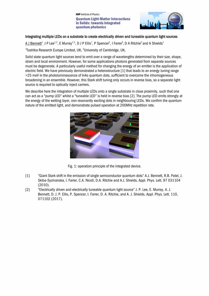
We describe here the integration of multiple LEDs onto a single substrate in close proximity, such that one can act as a “pump LED” whilst a “tuneable LED” is held in reverse bias [2]. The pump LED emits strongly at the energy of the wetting layer, non-resonantly exciting dots in neighbouring LEDs. We confirm the quantum nature of the emitted light, and demonstrate pulsed operation at 200MHz repetition rate.
Fig. 1: operation principle of the integrated device.
[1] “Giant Stark shift in the emission of single semiconductor quantum dots” A.J. Bennett, R.B. Patel, J. Skiba-Syzmanska, I. Farrer, C.A. Nicoll, D.A. Ritchie and A.J. Shields, Appl. Phys. Lett. 97 031104 (2010).
[2] “Electrically driven and electrically tuneable quantum light source” J. P. Lee, E. Murray, A. J. Bennett, D. J. P. Ellis, P. Spencer, I. Farrer, D. A. Ritchie, and A. J. Shields, Appl. Phys. Lett. 110, 071102 (2017).

5
(invited) Photonic trumpets for quantum optics and hybrid optomechanics
J-M Gérard
Institute for Nanoscience and Cryogenics, CEA, France
Over the last 20 years, quantum dots (QDs) have been fruitfully combined with optical microcavities to perform quantum optics experiments and to develop quantum light sources for QIPC. In this talk, I will show that the very basic photonic wire geometry opens an attractive alternative avenue in this context [1]. I will noticeably introduce the Photonic Trumpet (PT) [2], formed by a high-index single-mode waveguide and a conical tapering. Nearly perfect single-mode emission, low-divergence Gaussian radiation pattern, linear polarization control, efficient wavelength tuning based on strain effects, and high efficiency single photon emission (> 0.75 photon per pulse) are reported for a single QD embedded in a PT. The PT also appears as a very promising platform to explore the unique optical properties of one-dimensional atoms [3] and develop hybrid optomechanical systems where the interaction between the two-level quantum system and mechanical modes is mediated by strain [4].
Work done with J. Claudon, J Bleuse, M Munsch, P Stepanov and with the groups of JP Poizat, O Arcizet, A Auffèves, M Richard (CNRS I. Néel Grenoble), N Gregersen (DTU), M Munsch, M Poggio and R Warburton (U. Basel), who are gratefully acknowledged, and supported by the French National Research Agency via the ‘QDOT’ (ANR-16-CE09-0010) project. [1] J. Claudon et al, Nat. Photon. 4, 174 (2010); J Bleuse et al, Phys. Rev. Lett. 106, 103601 (2011);
M. Munsch et al, Phys. Rev. Lett. 108, 077405 (2012); P Stepanov et al, Appl. Phys. Lett. 106, 041112 (2015)
[2] M. Munsch et al, Phys. Rev. Lett. 110, 177402 and 239902(E) (2013); P Stepanov et al, Appl. Phys. Lett. 106, 041112 (2015)
[3] D. Valente et al, New J. Phys 14, 083029 (2012); Phys. Rev. A 86, 022333 (2012) [4] I. Yeo et al, Nat. Nano. 9, 106 (2014) ; P.L. de Assis et al, Phys. Rev. Lett. 118, 117401(2017); M.
Munch et al, Nature Comms 8, 76 (2017)
Au+ SiO2 mirror
1 µm
adiabatic taper
anti-reflection coating
InAs QD
Micrograph of a GaAs photonic trumpet.
Progress on optical fabrication and characterisation of SU-8 disc modulated mode-gap photonic crystal cavities
L P Nuttall1, F S F Brossard2, S A Lennon1, B P L Reid1, J Wu3, J Griffiths4, E Clarke5 and R A Taylor1 1 University of Oxford, UK, 2Hitachi Europe Ltd, UK, 3University College London, UK, 4 University of Cambridge, UK 5University of Sheffield, UK
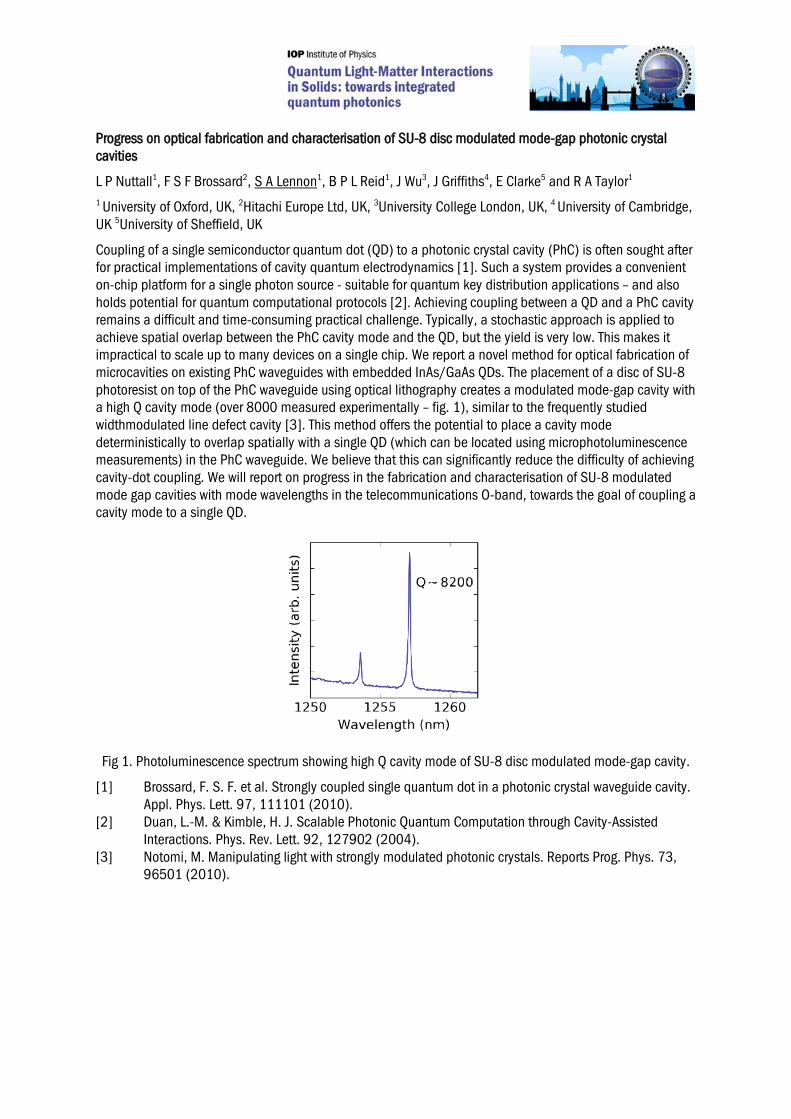
Coupling of a single semiconductor quantum dot (QD) to a photonic crystal cavity (PhC) is often sought after for practical implementations of cavity quantum electrodynamics [1]. Such a system provides a convenient on-chip platform for a single photon source - suitable for quantum key distribution applications – and also holds potential for quantum computational protocols [2]. Achieving coupling between a QD and a PhC cavity remains a difficult and time-consuming practical challenge. Typically, a stochastic approach is applied to achieve spatial overlap between the PhC cavity mode and the QD, but the yield is very low. This makes it impractical to scale up to many devices on a single chip. We report a novel method for optical fabrication of microcavities on existing PhC waveguides with embedded InAs/GaAs QDs. The placement of a disc of SU-8 photoresist on top of the PhC waveguide using optical lithography creates a modulated mode-gap cavity with a high Q cavity mode (over 8000 measured experimentally – fig. 1), similar to the frequently studied widthmodulated line defect cavity [3]. This method offers the potential to place a cavity mode deterministically to overlap spatially with a single QD (which can be located using microphotoluminescence measurements) in the PhC waveguide. We believe that this can significantly reduce the difficulty of achieving cavity-dot coupling. We will report on progress in the fabrication and characterisation of SU-8 modulated mode gap cavities with mode wavelengths in the telecommunications O-band, towards the goal of coupling a cavity mode to a single QD.
Fig 1. Photoluminescence spectrum showing high Q cavity mode of SU-8 disc modulated mode-gap cavity.
[1] Brossard, F. S. F. et al. Strongly coupled single quantum dot in a photonic crystal waveguide cavity. Appl. Phys. Lett. 97, 111101 (2010).
[2] Duan, L.-M. & Kimble, H. J. Scalable Photonic Quantum Computation through Cavity-Assisted Interactions. Phys. Rev. Lett. 92, 127902 (2004).
[3] Notomi, M. Manipulating light with strongly modulated photonic crystals. Reports Prog. Phys. 73, 96501 (2010).

7
(invited) Intrinsic phonon scattering limitations of on-demand quantum dot single-photon sources
S Hughes and C Gustin
Queen’s University, Canada
Quantum dots (QD) as artificial atoms are excellent candidates for solid-state quantum bits (qubits) and show promise for enabling scalable quantum information processing at optical frequencies. However, being part of a solid-state lattice structure, QD electron-hole pairs (excitons) are intrinsically coupled to the underlying phonon reservoir, which significantly reduces their coherence time on short time scales. Phonon dressing of QD emission now manifests itself in a number of optical effects, such as phonon-assisted inversion [1, 2], damping and frequency shifts of driven Rabi oscillations [3], excitation-induced dephasing of Mollow triplet sidebands [4, 5], and modified spontaneous emission [6], which distinguishes QDs from simple two-level atoms.
Of much interest for application in the emerging field of quantum information processing, as well as fundamental light-matter physics, is an “on-demand” source of single photons. These sources are usually required to be deterministic and efficient (one photon extracted per input triggering), as well as producing quantum mechanically indistinguishable photons, to allow for coherent two-photon interference. Semiconductor QDs coupled to optical cavities have emerged over the past two decades as highly promising candidates to achieve these ends, with recent experiments boasting sources with near-unity indistinguishability [8] and high efficiency in coupling to an output optical fiber [9]. However, these methods typically require polarization filtering to spectrally isolate the emitted photons from the pump light, thus reducing the efficiency.
In this talk, we will describe some of our result theory work on using a polaron master equation approach to understand a wide range of quantum light-matter interactions in QD cavity (and cavity-waveguide) systems. We then apply this approach to the biexciton-cascade system [7], and explore a method of coherently and deterministically exciting a QD coupled to a cavity which produces photons with simultaneously high efficiency and indistinguishability with orthogonal polarization to all input fields. This method, originally proposed in Ref. [10], utilizes an adiabatic Raman transition between different polarizations of excitons via the fourlevel biexciton-cascade, but is modified in the presence of electron-phonon scattering [11]. In particular, we analyze the system dynamics using a powerful cavity-QED polaron master equation approach, which captures important electron-phonon coupling nonperturbatively. We find that this cavity-assisted adiabatic passage single-photon source can produce photons with simultaneously over 90% efficiency and indistinguishability, using highly realistic experimental parameters. We also further investigate the operation of this source as a function of various system parameters, including laser and cavity detunings, temperature, and cavity width and elucidate the underyling physics in the context of the intrinsic electron-phonon scattering. In addition, we will discuss the intrinsic phonon limitations to resonantly driven QD-cavity systems as well, and speculate on some of the most promising routes and systems that lie ahead.
[1] S. Hughes and H. J. Carmichael, New J. Phys. 15, 053039 (2013); also see: Physics (Viewpoint) 8, 29 (2015).
[2] J. H. Quilter et al., Phys. Rev. Lett. 114, 137401 (2015). [3] A. J. Ramsay et al., Phys. Rev. Lett. 105, 177402 (2010). [4] C. Roy and S. Hughes, Phys. Rev. Lett. 106, 247403 (2011). [5] A. Ulhaq, S. Weiler, C. Roy, S. M. Ulrich, M. Jetter, S. Hughes, and P. Michler, Opt. Express 21, 4382
(2013). [6] K. Roy-Choudhury and S. Hughes, Optica 2, 434 (2015). [7] F. Hargart et al., Phys. Rev. B 93, 115308 (2016). [8] N. Somaschi et al., Nat. Phot. 10, 340 (2016). [9] R. S. Daveau et al., Optica 4, 178 (2017). [10] P. K. Pathak and S. Hughes, Phys. Rev. B 82, 0435308 (2010). [11] C. Gustin and S. Hughes,
Phys. Rev. B 96, 085305 (2017).

Circumventing phonon effects in optical state preparation of quantum dots using adiabatic rapid passage
D E Reiter1, S Lüker1, T Kaldewey2, A V Kuhlmann2,3, S R Valentin4, J-M Chauveau5, A Ludwig4, A D Wieck4, R J Warburton2 and T Kuhn1 1Westfälische Wilhelm-Universität Münster, Germany, 2University of Basel, Switzerland, 3IBM Research-Zurich, Switzerland 4Lehrstuhl für Angewandte Festkörperphysik, Ruhr-Universität Bochum, Germany 5Université Côte d’Azur, CNRS, France
In semiconductor quantum optics, the optical state preparation of semiconductor quantum dots (QDs) is the key ingredient for many applications in the field of quantum information technology. Because the QD is embedded in a crystal matrix the interaction with phonons plays a decisive role [1]. In this contribution we discuss how the influence of phonons can be circumvented resulting in a high fidelity preparation of the QD.
The excitation of a QD with a chirped laser pulse results in a robust population inversion due to the effect of adiabatic rapid passage (ARP). The interaction with phonons can be detrimental for the ARP effect. At low temperatures one finds that for negative chirp a damping occurs, while for positive chirp the ARP effect still results in a high fidelity preparation. This can be seen in Fig. 1, where we show measured (top) and calculated (bottom) data resulting from an excitation of a charged QD with a chirped laser pulse [2]. The reduced fidelity for negative chirp is caused by phonon emission processes, while the curve for positive chirp is essentially unaffected due to the absence of phonon absorption at low temperatures (here 4 K) [3]. At high pulse areas something remarkable happens: for both signs of the chirp a high fidelity preparation of the excited state occurs. Here, we have entered the so-called reappearance regime, which has already been predicted for Rabi rotations [4]. In the reappearance regime the phonon coupling is negligible. As a consequence the optical state preparation at these excitation conditions is also robust against elevated temperatures making it very attractive for optical state preparation.
In this contribution, we show experimental evidence together with theoretical calculations of entering the reappearance regime in a charged QD excited by chirped laser pulses [2]. We study the possibility to extend the ARP preparation scheme to elevated temperatures. The ARP effect can also be used to excite the biexciton in a neutral QD [5]. We further discuss, why ARP allows us to enter the reappearance regime, while for the standard Rabi rotations this is much harder to achieve.
Fig. 1: Experimentally measured emission due to resonance fluorescence of the trion transition (top) and
theoretically calculated occupation of the trion state (bottom) for an excitation with an essentially unchirped pulse (black lines), a positively chirped pulse (red lines) and a negative chirped pulse (blue lines) at 4 K [2].
For high pulse areas the phonon influence becomes negligible and the so-called reappearance regime is reached.
9
[1] D. E. Reiter, T. Kuhn, M. Glässl, and V. M. Axt, J. Phys.: Condens. Matter 26, 423203 (2014). [2] T. Kaldewey, D. E. Reiter et al., Phys. Rev. B 94, 241306(R) (2017). [3] S. Lüker, T. Kuhn, D. E. Reiter, Phys. Rev. B 85, 121302(R) (2012). [4] A. Vagov, M. D. Croitoru, V. M. Axt, T. Kuhn, and F. M. Peeters, Phys. Rev. Lett. 98, 227403 (2007). [5] T. Kaldewey, D. E. Reiter et al., Phys. Rev. B 94, 161302(R) (2017).
Quantum light-matter interaction at on-chip temperature conditions with a-plane InGaN quantum dots
T Wang1, T J Puchtler1, T Zhu2, S K Patra3, J C Jarman2, L P Nuttall1, C C Kocher1, S Schulz3, R A Oliver2 and R A Taylor1 1University of Oxford, UK, 2University of Cambridge, UK, 3University College Cork, Ireland
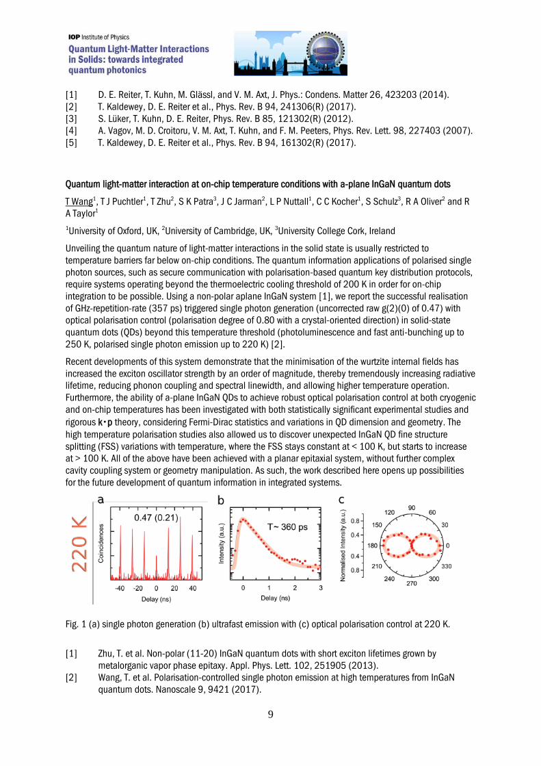
Unveiling the quantum nature of light-matter interactions in the solid state is usually restricted to temperature barriers far below on-chip conditions. The quantum information applications of polarised single photon sources, such as secure communication with polarisation-based quantum key distribution protocols, require systems operating beyond the thermoelectric cooling threshold of 200 K in order for on-chip integration to be possible. Using a non-polar aplane InGaN system [1], we report the successful realisation of GHz-repetition-rate (357 ps) triggered single photon generation (uncorrected raw g(2)(0) of 0.47) with optical polarisation control (polarisation degree of 0.80 with a crystal-oriented direction) in solid-state quantum dots (QDs) beyond this temperature threshold (photoluminescence and fast anti-bunching up to 250 K, polarised single photon emission up to 220 K) [2].
Recent developments of this system demonstrate that the minimisation of the wurtzite internal fields has increased the exciton oscillator strength by an order of magnitude, thereby tremendously increasing radiative lifetime, reducing phonon coupling and spectral linewidth, and allowing higher temperature operation. Furthermore, the ability of a-plane InGaN QDs to achieve robust optical polarisation control at both cryogenic and on-chip temperatures has been investigated with both statistically significant experimental studies and rigorous k‧p theory, considering Fermi-Dirac statistics and variations in QD dimension and geometry. The high temperature polarisation studies also allowed us to discover unexpected InGaN QD fine structure splitting (FSS) variations with temperature, where the FSS stays constant at < 100 K, but starts to increase at > 100 K. All of the above have been achieved with a planar epitaxial system, without further complex cavity coupling system or geometry manipulation. As such, the work described here opens up possibilities for the future development of quantum information in integrated systems.
Fig. 1 (a) single photon generation (b) ultrafast emission with (c) optical polarisation control at 220 K.
[1] Zhu, T. et al. Non-polar (11-20) InGaN quantum dots with short exciton lifetimes grown by metalorganic vapor phase epitaxy. Appl. Phys. Lett. 102, 251905 (2013).
[2] Wang, T. et al. Polarisation-controlled single photon emission at high temperatures from InGaN quantum dots. Nanoscale 9, 9421 (2017).

On-chip electro-mechanical routing of single photons from an embedded quantum emitter
Z K Bishop, A P Foster, Benjamin Royall, C Bentham, E Clarke, M S Skolnick and L R Wilson
University of Sheffield, Sheffield, UK
We demonstrate routing of single photons by electro-mechanical tuning of the splitting ratio (SR) of an optical beam splitter in the form of an on-chip directional coupler (DC). Single photons are generated by optical excitation of an InGaAs quantum dot (QD) embedded in the input arm of the fixed waveguide of the DC (Fig. 1(a)). The second of the two waveguides forming the DC is located at the free end of a cantilever. Applying a voltage between the cantilever and the substrate results in a capacitive force, which causes the cantilever to deflect towards the substrate. The resulting out-of-plane separation between the waveguides is used to control the SR of the DC operating at the single photon level.
The device was fabricated from a GaAs-based p-i-p-i-n diode. The DC and the cantilever were defined within the 160 nm thick p-i-p GaAs membrane containing InGaAs QDs, and were isolated from the n-GaAs substrate by a 2 µm thick intrinsic sacrificial AlGaAs layer. Each arm of the DC was terminated with a Bragg outcoupler (OC) to enable vertical collection of the transmitted photons. Electrical contacts were made to the top p and the bottom n layers so that charge can build up between the two under bias. The simulated displacement of the free end of the cantilever as a function of bias is shown in Fig. 1(b), with stable displacements of over 600 nm possible before pull-in.
The device was studied using micro-photoluminescence spectroscopy at 4 K. The emission from a single QD positioned in the input arm of the DC was recorded from both the through and the drop OCs (see Fig. 1(a)). Measured changes to the collected emission from the through OC versus cantilever displacement are presented in Fig. 1(c). At zero displacement photons emitted by the QD are split 80:20 between the through and drop ports of the DC respectively. As the cantilever displaces downwards by over 400 nm the signal change from the through OC increases monotonically until it saturates at 16 % at displacements of over 300 nm causing the SR to approach 100:0. The single-photon nature of the collected emission was verified with autocorrelation measurements, with normalized g (2)(0) = 0.25 ± 0.02.
Our approach provides local control of the splitting ratio of a directional coupler, a key building block of quantum optical circuits. It is inherently scalable and can be used to provide control of other individual photonic elements, such as Mach Zehnder interferometers, in more complex III-V semiconductor integrated quantum optical circuits.
Fig. 1: (a) SEM image of the device. (b) Simulated displacement of the free end of the cantilever as a
function of bias. (c) Changes to the QD signal collected from the through OC as a function of cantilever displacement. The continuous line is the theoretical curve.

11
Efficient classical algorithm for boson sampling with partially distinguishable photons
J J Renema1, A Menssen1, W R Clements1, G Triginer1, W S Kolthammer1,2 and I A Walmsley1
1 Oxford University, UK, 2Imperial College London, UK
Boson sampling provides a promising route towards demonstrating a quantum advantage, i.e. a computation by a quantum system that exceeds what is possible with a classical one. In boson sampling, the task is to provide a sample from the output of a linear transformation of optical modes, some of which are fed with single photons. For a sufficient number of photons, a suitable quantum machine directly implementing this problem will outperform a realistic classical computer simulating the experiment. A crucial challenge for boson sampling and problems inspired by it is to accommodate imperfections that arise in real-world devices. However, it is still an open question whether sampling tasks can be devised that retain their hardness under experimental conditions.
In this work, we provide a partial solution to this question. We use partial distinguishability of the interfering photons as an imperfection that compromises the hardness of a boson sampler, thereby demonstrating an explicit counter-example of classically efficient sampling. The basis of our algorithm is schematically depicted in Fig. 1: for partially distinguishable photons, the probability of a given outcome can be approximated by terms that involve fewer interfering photons, where the remaining ones do not interfere at all.
Fig. 1: schematic depiction of our result. Boson sampling with many photons of finite distinguishability can be approximated as boson sampling with fewer fully indistinguishable photons.
We find a bound on the indistinguishability required to demonstrate a quantum advantage by considering for which values of the error tolerance and photon number our algorithm is efficient. We find that for 50 photons and an error threshold of 10%, the degree of indistinguishability of the interfering photons must be higher than 94.7% (see Fig. 2). This result provides an effective lower bound in photon quality which a boson sampling experiment must clear to not be classically simulable.
Fig. 2: Minimum requirements on photon indistinguishability as function photon number
[1] Renema et al, arXiv:1707.02793

(invited) Solid state quantum optics on a chip
M S Skolnick
University of Sheffield, UK
Scalable quantum optics is a primary goal to achieve a multitude of applications in quantum information processing. Such scalability is likely to be achieved in a solid state environment. In this paper recent progress in Sheffield will be described in the field of III-V semiconductors where self-assembled quantum dots provide nearly ideal sources of single photons, and at the same time well-defined spin qubits, two of the main requirements for a scalable technology in a materials system with a well-developed fabrication technology.
The talk will describe three main topics, spin to path and path to spin conversion for quantum dots in waveguides, very high coherence single photons on chip, close to the transform limit and highly efficient scattering of single photons by single dots on chip, the route to single photon logic. In figure 1 the typical single mode waveguide geometry employed to demonstrate spin to path conversion is shown. Single photons emitted by spin up states propagate left and spin down to the right, a property of the chiral electromagnetic field in nano-photonic structures. In figure 2 the structure used to generate very high coherence single photons is shown. It consists of a very small volume photonic crystal cavity coupled to waveguide arms. Record modification of spontaneous emission rates is demonstrated by up to factor of 40 (see Fig 3 which shows radiative exciton lifetimes as short as 23 ps). A key feature is the tunability of quantum dot energies by the quantum confined Stark effect which allows tuning of the quantum dot into resonance with the photonic crystal cavity modes. In Fig 4 the tunable structure to demonstrate large modifications in transmission of single photons mediated by a single quantum dot is shown, with field-tunable changes in scattering of single photons of up to 30% found (Fig 5), showing excellent coupling of the single quantum state to the nanophotonic mode, and providing the route to single photon phase shifters and logic gates.

13
Highly polarized electrically driven single photon emission from a non-polar InGaN quantum dot
C C Kocher1, T Puchtler1, J C Jarman2, T Zhu2, R A Oliver2 and R A Taylor1 1University of Oxford, UK, 2University of Cambridge, UK
We report on successful electrical excitation of non-polar a-plane InGaN quantum dots (QDs). These were grown employing MOVPE with a method similar to the Stranski Krastanov mode. The QDs lie within an electrically contacted p-i-n diode. As previously shown with photoluminescence studies, these QDs are sources of highly linearly polarised single photons.
Here, we present a study of the polarisation properties of the electroluminescence of these QDs. A very high degree of linear polarisation is measured, deterministically linked to a special crystal direction. Furthermore, we study the second order correlation function of a QD under DC excitation and find evidence for single-photon emission with a g(0)=0.18, corrected for the instrument response function. This is very low for electrically driven nitride QDs. Finally, we probe the temperature dependence up to 80K of the same spectral line, underlining its assignment to a QD.
Our approach to obtain electroluminescence differs from most previous studies on InGaN QDs by using planar epitaxial growth as opposed to either growing QDs as restricted quantum wells in nano-pillars or etching QDs out of quantum wells. In contrast to the latter, our method allows for future development towards structures such as photonic crystal cavities. Thus, our work presented here is a major step towards the development of a highly polarised, efficient, electrically pumped single-photon source.
(invited) Cavity QED with carbon nanotubes
A Jeantet, T Claude, Y Chassagneux, C Raynaud, Ph Roussignol, and C Voisin
Ecole Normale Supérieure, France
Coupling a carbon nanotube to a photonic resonator in a reliable way is highly desirable for technological developments in view of quantum cryptography or quantum computation. Moreover, the low-cost, the high integrability and the possible electrical excitation of nanotubes are attractive assets in such perspectives. However, due to the lack of control of the current growth or deposition processes, current attempts rely on random spectral and spatial matching between a resonator and randomly deposited nanotubes, leading to a very limited fabrication yield. We propose an original approach where the nanotube is fully characterized in free-space by regular low-temperature micro-photoluminescence spectroscopy and where an optical cavity is subsequently formed around the emitter by approaching a concave dielectric mirror micro-engineered at the apex of an optical fiber. This geometry brings an unprecedented flexibility giving a built-in spectral and spatial matching, together with excellent quality factors and mode volumes. Individual carbon nanotubes embedded in a polystyrene matrix are coupled to the cavity resulting in a strong brightening of the nanotube of more than an order of magnitude, bringing evidence for the relevance of exploiting cavity quantum electrodynamical (CQED) effects to enhance the photonic properties of carbon nanotubes. By means of time-resolved measurements we investigate directly the cavity enhanced emission rate and find a corresponding Purcell factor of up to 5. Finally, by adjusting the cavity length, we are able to tune the working wavelength of the emitter over 10 nm (4 THz) while keeping a high-spectral purity of the source (below 80 GHz) by exploiting the cavity feeding effect [1] on the acoustic phonon side-bands of the luminescence of the nanotube.
[1] A. Auffèves, J.-M. Gérard, and J.-P. Poizat, Phys. Rev. A 79, 053838 (2009).

Effect of excitation conditions on the purity of quantum emission from InGaN
H P Springbett1,2*, K Gao2, T Zhu1, M Holmes2, Y Arakawa2 and R A Oliver1 1University of Cambridge, UK, 2The University of Tokyo, Japan
The III-nitride materials system displays many advantages for use as single photon sources. The tuneability of the emission wavelength to blue, green and red [1] is particularly beneficial as it is this region where ultrafast single photon detectors display greatest sensitivity, and the size of transmitter and receiver optics for free-space cryptography could be reduced. Furthermore, the possibility of high-temperature emission [2,3] eliminates the need for expensive cryogenic cooling.
In this work, we present a study on methods by which to improve the purity of the extracted single photon emission from samples of self-assembled InGaN quantum dots emitting at wavelengths from 420nm to 470 nm, enhanced by meso-porous distributed Bragg Reflectors. Autocorrelation measurements were performed using a Hanbury-Brown and Twiss type setup and using a frequency tripled tuneable Ti:Al2O3 pulsed laser to perform excitation both below and above the bandgap of the host GaN crystal. A large suppression in uncorrelated background emission was achieved by etching the sample into micropillar structures. Greatly improved values of g(2)(0) were then achieved by tuning the laser below the GaN bandgap, and appropriately choosing the excitation power to further reduce the background emission. Figure 1 shows a series of measured 𝑔(2)(0) values under various excitation conditions. By tuning the excitation wavelength to 400nm and reducing the excitation power we are able to achieve a 𝑔(2)(0) value of ~0.12. Additional experiments are being performed to further optimize the single photon emission and extraction.
Fig.1. Excitation power and wavelength dependence of the measured g(2)(0) values of the emission from an
InGaN quantum dot emitting at a wavelength of 450nm.
[1] Deshpande, S et al., Electrically pumped single-photon emission at room temperature from a single InGaN/GaN quantum dot, Applied Physics Letters 105, 141109 (2014)
[2] Wang, T. et al., Polarisation-controlled single photon emission at high temperatures from InGaN quantum dots, Nanoscale 9 (27), 9421-9427 (2016)
[3] Holmes, M. et al., Single photons from a hot solid-state emitter at 350 K, ACS Photonics, 3 (4), 543-546 (2016)

15
Optical properties of topological insulator nanoparticles
G Siroki, P D Haynes, D K K Lee, P A, Huidobro and V Giannini
Imperial College London, UK
Topological insulators are materials that have metallic surface states protected by time-reversal symmetry. Such states are delocalised over the surface and are immune to non-magnetic defects and impurities.
Building on previous work [1] we have studied the interaction of light with a topological insulator nanoparticle. Our main finding is that the occupied surface states can lead to charge density oscillations akin to plasmons in metallic nanoparticles. Furthermore, these oscillations can couple to phonons forming a previously unreported excitation [2]. Because the states are localised at the surface, a small number of them is enough to change the absorption spectrum of the particle containing many thousands of atoms. We will show how the effect can be adjusted by varying the particle's size and shape. Furthermore, we will discuss similarities and differences with microcavities of photonic crystals that display topological properties [3].
To summarize, the protected surface states add an additional degree of freedom to tune the optical properties of topological insulator nanoparticles. The present findings may be interesting for researchers working on cavity electrodynamics and quantum information.
[1] K Imura, Y Yoshimura, Y Takane, T Fukui, Phys Rev B 86, 235119 (2012) [2] G Siroki, D K K Lee, P D Haynes, V Giannini, Nat Comm 7, 12375 (2016) [3] G Siroki, P A Huidobro, V Giannini, Phys Rev B 96, 041408(R) (2017)

Multimode polariton solitons in microcavity wires for polaritonic integrated circuits
G Slavcheva1, 2, M Koleva3 and A Pimenov4 1University of Bath, UK, 2Johannes Kepler University Linz, Austria, 3University of Oxford, Oxford, UK, 4Weierstrass Institute, Germany
Integrated optical technologies for quantum computing based on linear optics have been under active development in the recent decade. However, nonlinear optical interactions ’on a chip’ offer new unexplored functionalities and may play a key role. Recently a new class of nonlinear system has emerged in which light and matter play equally important roles. The basic building blocks of these systems are quantum states of matter coupled to enhanced optical fields found in microstructures. One example is the microcavity exciton-polariton: a mixed light-matter quasiparticle, resulting from the strong coupling of quantum well excitons to cavity photons. Polariton waves can be confined in structures with sub-micron size and laterally etched microcavity wires enhance further the polaritonic nonlinearities. This enables fabrication of polaritonic integrated circuits based on structured semiconductor microcavities on a chip.
Fig. 1: (a) Scheme of the microcavity wire and the excitation geometry; (b) Linear polariton dispersion for the
fundamental and 5 higher-order modes at ∆ = 0, wire width w = 3 µm; Bistability (∆ = −0.1) (c) and Multistability (∆ = 0) (d) curves.
In this talk, I will focus on the potential of self-localised structures, such as bright polariton solitons [1], to be exploited for signal processing in polaritonic networks on a chip, which will pave the way towards quantum polaritonic integrated circuits. I will introduce our new driven-dissipative mean-field model of nonlinear polariton dynamics in non-planar microcavity wires and will discuss interesting model predictions. We found composite ’multimode’
Figure 2: (a) Snapshot at t = 80 ps of the soliton at ∆ = 0 and γ = 0.04 for Ep = 0.075 and longitudinal cross-sections; (b) Soliton in a tilted wire (α = 5◦ ); (c,d) time evolution of a soliton in a tapered wire.
polariton solitons that result from the superposition of multiple co-existing transverse cavity modes [2] and are more robust to disorder. The typical microcavity nonlinear optical bistability evolves into a spatial multi-stability upon pump amplitude variation(Fig.1). We have developed a modal expansion model to investigate and control the intermodal nonlinear interactions and localisation of coupled-mode solitons [3]. Conditions for multimode polariton soliton formation, domains of existence and geometry limitations for stable propagation have been identified (Fig.2) [4].
[1] M. Sich et al., Nature Photonics, 6, 50–55 (2012)

17
[2] G. Slavcheva, A. V. Gorbach, A. Pimenov, A. G. Vladimirov and D. V. Skryabin, Opt. Lett. 40, 1787 (2015)
[3] G. Slavcheva, A. V. Gorbach, and A. Pimenov, Phys. Rev. B 94, 245432 (2016) [4] G. Slavcheva, M. V. Koleva, and A. Pimenov, J. of Optics 19, 065404 (2017)

High principal quantum number excitons in cuprous oxide semiconductor crystal
J P Rogers, C Hodges, C S Adams, M P A Jones, W W Langbein and S A Lynch
University of Durham, UK
The highly-excited Rydberg states of atoms exhibit properties that make them of particular interest in the field of quantum information processing. Recently in the field of quantum optics, it has been demonstrated that the strong interactions of Rydberg states with their environment, whether neighbouring particles or perturbing fields, can be mapped onto light [1]. Non-linear phenomena, such as the Rydberg blockade effect in species such as gaseous Sr and Rb, have been exploited to generate qubits and entangled photon pairs [2].
For application, conventional electronics and photonics are undoubtedly more simply integrated with solid-state systems than with cold atom clouds. A Rydberg-like series of spectral lines have been observed in a variety of semiconductor materials due to the formation of excitons. A series of 8 sharp optical resonances just below the conduction band in Cu2O were first observed in the 1950s. A breakthrough was made [3] in 2014 when the Fröhlich group in Dortmund resolved excitation peaks up to the principal quantum number n = 25.
A collaboration between the University of Durham and the University of Cardiff has been established with the aim of mapping the Rydberg phenomena observed in quantum atomic optics onto the excitons manifest in Cu2O solid state system. I will present the preliminary data produced by the Cardiff group, represented in the figure below, and discuss our plans for future work.
Fig. 1: The absorbance peaks due to Rydberg excitons in Cu2O semiconductor crystal at 6.5 K. Each state is
labelled with its corresponding principal quantum number, n.
[1] D. Maxwell et. al., Physical Review Letters, 110, 103001, 2013 [2] L. I. R. Gil et al., Physical Review Letters, 112, 103601, 2014 [3] T. Kazimierczuk et. al., Nature, 514, 343, 2014

19
Photonic waveguides for 780 nm optical delivery for quantum sensors based on Ultra-cold atoms of Rubidium
J O Maclean1, M T Greenaway2, R P Campion1, M Wildman1, T M Fromhold1 and C J Mellor1 1University of Nottingham, UK, 2Loughborough University, UK
An on-chip approach to optical delivery for portable quantum sensors is described. The optical design, epitaxy, nanofabrication and measurement of polarisation-maintaining, deep-etched aluminium gallium arsenide (AlxGa(1-x)As) waveguides for near-infra-red 780 nm light was achieved, in an analogous approach to earlier work at (1300-1550) nm wavelengths [1]. Material characterisation techniques were developed to infer improved optical quality and reduced optical loss intrinsic to the material, grown by Molecular Beam Epitaxy (MBE). High, continuous-wave optical power densities were guided with low polarisation noise and photonic waveguide performance was stable over time. The optical loss was measured to be below 4.3(±0.4) dB cm-1 corresponding to an attenuation coefficient, α, of 1.0 (±0.08) cm-1 for single mode waveguides and demonstrating improved performance data [2]. The polarisation extinction ratio was better than -19 (±1) dB for orthogonal polarisations.
These novel components illustrate the feasibility of passive photonic integrated circuits for the 780 nm wavelength. Future work will investigate the optical switching properties of these structures. The ultimate aim of the work is the creation of waveguidebased photonic circuits for compact cold atom sensors based on the D2 hyperfine transition of 87Rb at 780.24 nm [3]. Further applications include free-space short-wave communications, hybrid quantum systems [4] and epitaxial structures transparent to shorter wavelengths for other cold atom species and trapped ions.
[1] Heaton, J.M., Bourke, M.M., Jones, S.B., Smith, B.H., Hilton, K.P., Smith, G.W., Birbeck, J.C.H., Berry, G., Dewar, S.V. and Wight, D.R., “Optimization of Deep-etched, Single-mode GaAs / AlGaAs Optical Waveguides using Controlled Leakage into the Substrate”, Journal of Lightwave Technology, 17(2), 267-281 (1999).
[2] Maclean, J.O., Greenaway, M.T., Campion, R.P., Pyragius, T., Fromhold, T.M., Kent, A.J., Mellor, C.J., “III-V semiconductor waveguides for photonic functionality at 780 nm” Proc. SPIE 8988, Integrated Optics: Devices, Materials, and Technologies XVIII, 898805 (2014)
[3] Bongs, K., Malcolm, J., Ramelloo, C., Zhu, L., Boyer, V., Valenzuela, T., Maclean, J., PiccardoSelg, A., Mellor, C., Fernholz, T., Fromhold, M., Krüger, P., Hellmig, O., Grote, A., Dörscher, S., Duncker, H., Windpassinger, P., Sengstock, K., Becker, C., Pelle, B., Hilico, A., Angonin, M.-C., Wolf, P., Pereira Dos Santos, F., Bertoldi, A., Bouyer, P., de Angelis, M., Prevedelli, M., Poli, N., Sorrentino, F., Tino, G., Stellmer, S., Schreck, F., Popp, M., Herr, W., Wendrich, T., Ertmer, W., Rasel, E., Kürbis, C., Peters, A., Wicht, A., “iSense: A Technology Platform for Cold Atom Based Quantum Technologies” Optics InfoBase Conference Papers [1-55752-995-7] (2014)
[4] Gleyzes, S., El Amili, A., Cornelussen, R.A., Lalanne, P., Westbrook, C.I., Aspect, A., Esteve, J., Moreau, G., Martinez, A., Lafosse, X., Ferlazzo, L., Harmand, J. C., Mailly, D. and Ramdane, A., "Towards a monolithic optical cavity for atom detection and manipulation," European Physical Journal D, 53(1), 107-111 (2009).
Acknowledgements: We should like to thank Dr M.C. Rosamond and Prof. E.H. Linfield for expertise in Electron Beam Lithography at the School of Electronic and Electrical Engineering, University of Leeds and for funding from the Engineering and Physical Sciences Research Council UK Quantum Technologies Hub for Sensors and Metrology, SM-30535 EP/M013294/1.

Programme and Abstract Book
Institute of Physics76 Portland Place, London W1B 1NT, UK
Telephone: +44 (0)20 7470 4800www.iop.org/conferences
Registered charity number 293851 (England & Wales) and SC040092 (Scotland)