qualcomm snapdragon processor
TRANSCRIPT

1
CHAPTER-1
INTRODUCTION
Qualcomm Inc. is an American global semiconductor company that
designs and markets wireless telecommunications products and services. The
company headquarters are located in San Diego, California, United States. The
company has 157 worldwide locations. The parent company is Qualcomm
Incorporated (Qualcomm), which includes the Qualcomm Technology Licensing
Division (QTL). Qualcomm's wholly owned subsidiary, Qualcomm Technologies,
Inc. (QTI), operates substantially all of Qualcomm's R&D activities, as well as its
product and services businesses, including its semiconductor business, Qualcomm
CDMA Technologies.
In November 2014, Qualcomm CEO Steve Mollenkopf announced at the
company’s annual analyst day meeting held in New York City that the company is
planning to target the data center market with new server chips based on the ARM
architecture and plans to make them commercially available by the end of 2015.
1.1 What is Snapdragon
Snapdragon is a suite of system-on-chip (SoC) semiconductor products
designed and marketed by Qualcomm for mobile devices. The Snapdragon central
processing unit (CPU) uses the ARM RISC instruction set, and a single SoC may
include multiple CPU cores, a graphics processing unit (GPU), a wireless modem,
and other software and hardware to support a smart phone's global positioning
system (GPS), camera, gesture recognition and video. Snapdragon semiconductors
are embedded in most Google Android and Windows Phone devices. They are
also used for net books, in cars, wearable devices and other devices.
The first Snapdragon product to be made available to consumer device
manufacturers was the QSD8250, which was released in November 2007. It
included the first 1 GHz processor for mobile phones. Qualcomm introduced its

2
"Krait" microprocessor architecture in the second generation of Snapdragon SoCs
in 2011, allowing each processor core to adjust its speed based on the device's
needs. At the 2013 Consumer Electronics Show, Qualcomm introduced the first of
the Snapdragon 800 series and renamed prior models as the 200, 400 and 600
series. Several new iterations have been introduced since, such as the Snapdragon
805, 810, 615 and 410. Qualcomm re-branded its modem products under the
Snapdragon name in December 2014.[1]
1.2 History
1.2.1 Pre-release
Qualcomm announced it was developing the Scorpion central processing
unit (CPU) in November 2005. The Snapdragon system on chip (SoC) was
announced in November 2006 and included the Scorpion processor, as well as
other semiconductors. This also included Qualcomm's first
custom Hexagon digital signal processor (DSP).
According to a Qualcomm spokesperson, it was named Snapdragon,
because "Snap and Dragon sounded fast and fierce." The following month,
Qualcomm acquired Airgo Networks for an undisclosed amount; it said Airgo's
802.11a/b/g and 802.11n Wi-Fi technology would be integrated with the
Snapdragon product suite. Early versions of Scorpion had a processor core design
similar to the Cortex-A8.[1]
1.2.2 Early Snapdragon products
The first Snapdragon shipments were of the QSD8250 in November 2007.
According to CNET, Snapdragon's "claim to fame" was having the first 1 GHz
mobile phone processor. Most smartphones at the time were using 500 MHz
processors. The first generation of Snapdragon products supported a 720p
resolution, 3D graphics and a 12-megapixel camera. By November 2008, 15
device manufacturers decided to embed Snapdragon semiconductors in their
consumer electronics products.
In November 2008, Qualcomm announced it would also compete against
Intel in the netbook processor market with dual-core Snapdragon system-on-chips
planned for late 2009. It demonstrated a Snapdragon processor that consumed less

3
power than Intel chips announced around the same time and claimed it would also
cost less when released. That same month, Qualcomm introduced a Snapdragon-
based protoytpe netbook called Kayak that used 1.5 GHz processors and was
intended for developing markets.
In May 2009, Java SE was ported and optimized for Snapdragon. At the
November 2009 Computex Taipei show, Qualcomm announced the QSD8650A
addition to the Snapdragon product suite, which was based on 45 nanometer
manufacturing processes. It featured a 1.2 GHz processor and had lower power
consumption than prior models.[1]
1.2.3 Adoption
By late 2009, smartphone manufacturers announced they would be using
Snapdragon semiconductors in the Acer Liquid Metal, HTC HD2, Toshiba
TG01 and the Sony Ericsson Xperia X10. Lenovo announced the first netbook
product using Snapdragon SoCs that December. According to PC World, mobile
devices using Snapdragon had better battery life and were smaller in size than
those using other SoCs.
By June 2010, Snapdragon chips were embedded in 20
available consumer devices and incorporated into 120 product designs in
development. Apple had a dominant market position for smartphones at the time
and did not incorporate Snapdragon into any of its products. The success of
Snapdragon therefore relied on competing Android phones, such as Google's
Nexus One and the HTC Incredible, challenging Apple's market position. Android
devices did end up taking market share from the iPhone and predominantly used
Snapdragon. As of July 2014, the market share of Android phones had grown to
84.6 percent. There was an "unconfirmed but widely circulated report" speculating
that Apple was going to start using Snapdragon SoCs in Verizon-based iPhones.
As of 2012, Apple was still using their own semiconductor designs. Support for
desktop Windows operating systems was added to Snapdragon in October 2010.
By 2011 Snapdragon was embedded in Hewlett Packard's WebOS devices and had
a 50% market share of a $7.9 billion smartphone processor market. By 2015,
Snapdragon was used in most non-Apple smartphones.
Snapdragon chips are also used in most Android-based smartwatches,
Snapdragon products have also been used in virtual reality products, in vehicles
like the Maserati Quattroporte and Cadillac XTS and in other applications.

4
1.2.4 Later models
In June 2010, Qualcomm began sampling the third generation of
Snapdragon products; two dual-core 1.2 GHz system on chips (SoC) called the
Mobile Station Modem (MSM) 8260 and 8660. GSM, UMTS and HSPA+
networks, while the 8660 was for CDMA2000 and EVDO networks.That
November Qualcomm announced the MSM8960 for LTE networks. In early 2011,
Qualcomm announced a new processor architecture called Krait, which used the
ARM v7 instruction set, but was based on Qualcomm's own processor design. The
processors were called S4 and had a feature named Asynchronous Symmetrical
Multi-Processing (aSMP), meaning each processor core adjusted its clock speed
and voltage based on the device's activity in order to optimize battery usage. Prior
models were renamed to S1, S2 and S3 to distinguish each generation.
The S4-based generation of Snapdragon SoCs began shipping to product
manufacturers with the MSM8960 in February 2012. In benchmark tests by
Anandtech, the MSM8960 had better performance than any other processor tested.
In an overall system benchmark, the 8960 obtained a score of 907, compared to
528 and 658 for the Galaxy Nexus and HTC Rezound respectively. In a Quadrant
benchmark test, which assesses raw processing power, a dual-core Krait processor
had a score of 4,952, whereas the quad-core Tegra 3 was just under 4,000.
Furthermore, another test using a dual-core Krait-powered HTC One Sproduced a
Quadrant score of 6,723 under Android 4.1.1. The quad-core version, APQ8064,
was made available in July 2012. It was the first Snapdragon SoC to use
Qualcomm's Adreno 320 graphics processing unit (GPU).[1]
1.2.5 Recent developments
Adoption of Snapdragon contributed to Qualcomm's transition from a
wireless modem company to one that also produces a wider range of hardware and
software for mobile devices. In July 2011 Qualcomm acquired GestureTek in
order to incorporate its gesture recognition intellectual property into Snapdragon
SoCs. In mid-2012 Qualcomm announced the Snapdragon software development
kit (SDK) for Android devices at the Uplinq developer conference. The SDK
includes tools for facial recognition, gesture recognition, noise cancellation and
5
audio recording. That November Qualcomm acquired some assets from EPOS
Development in order to integrate its stylus and gesture recognition technology
into Snapdragon products. It also collaborated with Microsoft to
optimize Windows Phone 8 for Snapdragon semiconductors.
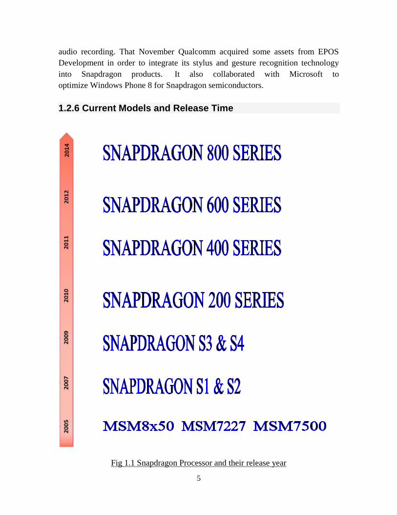
1.2.6 Current Models and Release Time
Fig 1.1 Snapdragon Processor and their release year
6
CHAPTER-2
SNAPDRAGON DEVICES
Snapdragon is a family of mobile systems on a chip (SoC) made by
Qualcomm for use in smart phones, tablets, and smart book devices. A system on
a chip or system on chip (SoC or SOC) is an integrated circuit (IC) that integrates
all components of a computer or other electronic system into a single chip. It may
contain digital, analog, mixed-signal, and often radio-frequency functions—all on
a single chip substrate.[2]
2.1 Different types of Snapdragon processors
List of different Snapdragon processor devices is given below.
1. Snapdragon S1
2. Snapdragon S2
3. Snapdragon S3
4. Snapdragon S4
5. Snapdragon 200 series
6. Snapdragon 400 series
7. Snapdragon 600 series
8. Snapdragon 800 series
2.2 Snapdragon S1
Qualcomm Snapdragon S1 is the first SoC (System on chip) marked by
Qualcomm in 2007.Basic specification and details are as discussed below.
2.2.1 Central Processing Unit
The Qualcomm Snapdragon S1 has an average performing CPU with a
maximum clock speed of 1,000.00 MHz. It has 1 core(s), resulting in fair to
middling multi-tasking when compared to most dual core processors.[3]

7
2.2.2 Graphics Processing Unit
The Qualcomm Adreno is a separate graphics processor solely intended for
the accelerated creation of images to be outputted to a display. Its entire
architecture is structured around processing large blocks of data in parallel.
Each API provides an interface for high-level languages to utilize the
graphics processing options in order to deliver better graphics for various
applications.
2.2.3 Digital Signal Processing
The Qualcomm Snapdragon S1 has a specialized digital signal
microprocessor that is used for the low-power operation of a device in applications
that deal with analog signals such as audio, video, and mobile broadband signals.
Each analog signal is converted into a digital signal that is then processed by the
DSP at a lower latency (relative to the CPU running the same digital signal
processing algorithm), thus improving performance.
2.2.4 External Components
External Component
Interfaces
Embedded GPS Module
RAM Interface LPDDR2 SDRAM
Video Encoding 720p
GPS Module Type Embedded Gen 7 gpsOne GPS module with
gpsOneXTRA Assistance
Table 2.1 External Component of Snapdragon S1
8
Model number
Semi conductor technology
CPU instruction set
CPU CPU
cache (in KB)
RAM Year
MSM7225 65 nm ARMv6 Up to 528 MHz ARM11 2007
MSM7625 65 nm ARMv6 Up to 528 MHz ARM11 2007
MSM7227 65 nm ARMv6 Up to 800 MHz ARM11 166 MHz LPDDR1
2008
MSM7627 65 nm ARMv6 Up to 800 MHz ARM11 166 MHz LPDDR1
2008
MSM7225A 45 nm ARMv7 Up to 800 MHz ARM Cortex-A5
200 MHz LPDDR1
Q4 2011
MSM7625A 45 nm ARMv7 Up to 800 MHz ARM Cortex-A5
200 MHz LPDDR1
Q4 2011
MSM7227A 45 nm ARMv7 Up to 1.0 GHz ARM Cortex-A5
L2: 256 200 MHz LPDDR1
Q4 2011
MSM7627A 45 nm ARMv7 Up to 1.0 GHz ARM Cortex-A5
L2: 256 200 MHz LPDDR1
Q4 2011
MSM7225AB 45 nm ARMv7 1 GHz ARM Cortex-A5
QSD8250 65 nm ARMv7 Up to 1 GHz Scorpion L2: 256 Q4 2008
QSD8650 65 nm ARMv7 Up to 1 GHz Scorpion L2: 257 Q4 2008
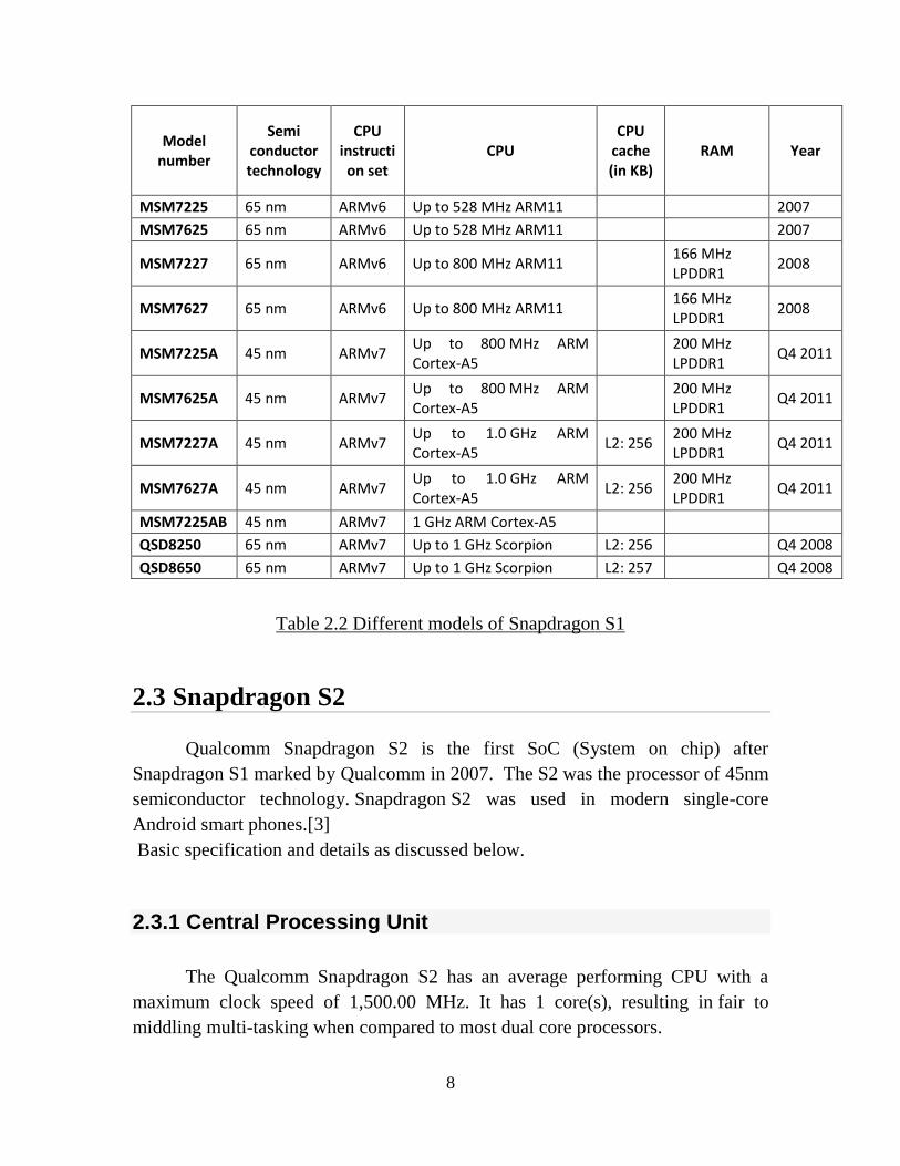
Table 2.2 Different models of Snapdragon S1
2.3 Snapdragon S2
Qualcomm Snapdragon S2 is the first SoC (System on chip) after
Snapdragon S1 marked by Qualcomm in 2007. The S2 was the processor of 45nm
semiconductor technology. Snapdragon S2 was used in modern single-core
Android smart phones.[3]
Basic specification and details as discussed below.
2.3.1 Central Processing Unit
The Qualcomm Snapdragon S2 has an average performing CPU with a
maximum clock speed of 1,500.00 MHz. It has 1 core(s), resulting in fair to
middling multi-tasking when compared to most dual core processors.

9
This processor is based on the Reduced Instruction Set
Computing (RISC) design strategy enabling instructions to execute faster, as
opposed to the Complex Instruction Set Computing (CISC) design strategy, which
is generally slower at executing due to lengthy instructions.
2.3.2 Graphics Processing Unit
The Qualcomm Adreno 205 GPU is a separate graphics processor solely
intended for the accelerated creation of images to be outputted to a display. Its
entire architecture is structured around processing large blocks of data in parallel.
Each API provides an interface for high-level languages to utilize the
graphics processing options in order to deliver better graphics for various
applications.
2.3.3 Digital Signal Processing
Hexagon QDSP5 256MHz The Qualcomm Snapdragon S2 has a
specialized digital signal microprocessor that is used for the low-power operation
of a device in applications that deal with analog signals such as audio, video, and
mobile broadband signals. Each analog signal is converted into a digital signal that
is then processed by the DSP at a lower latency (relative to the CPU running the
same digital signal processing algorithm), thus improving performance. [3]
2.3.4 External Components
External Component
Interfaces Bluetooth 4.0
Display Support
RAM Interface 333MHz LPDDR2
Table 2.3 External Component of Snapdragon S2

10
Model number
Semi conductor technology
CPU instruction
set CPU
CPU cache (in KB)
RAM Year
MSM7230 45 nm ARMv7 Up to 800 MHz Scorpion
L2: 256 Dual-channel 333 MHz LPDDR2
Q2 2010
MSM7630 45 nm ARMv7 Up to 800 MHz Scorpion
L2: 256 Dual-channel 333 MHz LPDDR2
Q2 2010
APQ8055 45 nm ARMv7 Up to 1.4 GHz Scorpion
L2: 256 Dual-channel 333 MHz LPDDR2
Q2 2010
MSM8255 45 nm ARMv7 Up to 1 GHz Scorpion
L2: 384 Dual-channel 333 MHz LPDDR2
Q2 2010
MSM8255T 45 nm ARMv7 Up to 1.5 GHz Scorpion
L2: 384 Dual-channel 333 MHz LPDDR2
Q2 2010
MSM8655 45 nm ARMv7 Up to 1 GHz Scorpion
L2: 384 Dual-channel 333 MHz LPDDR2
Q2 2010
MSM8655T 45 nm ARMv7 Up to 1.5 GHz Scorpion
L2: 384 Dual-channel 333 MHz LPDDR2
Q2 2010
Table 2.4 Different models of Snapdragon S2
2.4 Snapdragon S3
The Qualcomm Snapdragon S3 is an entry level SoC for smartphones and
tablets (mostly Android based). It contains two Scorpion cores (enhanced ARM
Cortex-A8) clocked at up to 1.7 GHz, a Adreno 220 graphics card and radio
elements. [3]

11
2.4.1 Central Processing Unit
The Qualcomm Snapdragon S3 has an average performing CPU with a
maximum clock speed of 1,700.00 MHz. It has 2 core(s), resulting in good multi-
tasking when compared to a single core processor.
As a result of following the Harvard architecture, the CPU has a separate
Level 1 instruction and data cache leading to a slight improvement in performance
over a unified Level 1 cache. The instruction cache is only used for storing
instructions and executes in a sequential manner. The data cache stores data used
by instructions; the point of access or storage is generally specified by an
instruction.
This processor is based on the Reduced Instruction Set Computing (RISC)
design strategy enabling instructions to execute faster, as opposed to the Complex
Instruction Set Computing (CISC) design strategy, which is generally slower at
executing due to lengthy instructions.
2.4.2 Graphics Processing Unit
The Qualcomm Adreno 220 is a separate graphics processor solely intended
for the accelerated creation of images to be outputted to a display. Its entire
architecture is structured around processing large blocks of data in parallel.
2.4.3 Digital Signal Processing
The Qualcomm Snapdragon S3 has a specialized digital signal
microprocessor that is used for the low-power operation of a device in applications
that deal with analog signals such as audio, video, and mobile broadband signals.
Each analog signal is converted into a digital signal that is then processed by the
DSP at a lower latency (relative to the CPU running the same digital signal
processing algorithm), thus improving performance. [3]
2.4.5 External Components
RAM Interface LPDDR2 SDRAM
Primary Camera Support 16 MP
Video Encoding 1080p
Video Decoding 1080p
GPS Module Type gpsOneGen 8 with GLONASS,
gpsOneXTRA Assistance

12
Table 2.5 External Component of Snapdragon S3
Model number
Semi conductor technology
CPU instruction set
CPU CPU cache (in KB)
RAM Year
APQ8060 45 nm ARMv7 Up to 1.7 GHz dual-core Scorpion
L2: 512 Single-channel 500 MHz ISM/333 MHz LPDDR2
2011
MSM8260 45 nm ARMv7 Up to 1.7 GHz dual-core Scorpion
L2: 512 Single-channel 500 MHz ISM/333 MHz LPDDR2
Q3 2010
MSM8660 45 nm ARMv7 Up to 1.7 GHz dual-core Scorpion
L2: 512 Single-channel 500 MHz ISM/333 MHz LPDDR2
Q3 2010
Table 2.6 Different models of Snapdragon S3
2.5 Snapdragon S4
The S4-based generation of Snapdragon SoCs began shipping to product
manufacturers with the MSM8960 in February 2012. In benchmark tests by Anand
tech, the MSM8960 had better performance than any other processor tested. In an
overall system benchmark, the 8960 obtained a score of 907, compared to 528 and
658 for the Galaxy Nexus and HTC Rezound respectively.
2.5.1 Central Processing Unit
The Qualcomm Snapdragon S4 Pro MSM8960AB has an average
performing CPU with a maximum clock speed of 1,728.00 MHz. It has 2 core(s),
resulting ingood multi-tasking when compared to a single core processor.
As a result of following the Harvard architecture, the CPU has a separate
Level 1 instruction and data cache leading to a slight improvement in performance
over a unified Level 1 cache. The instruction cache is only used for storing
instructions and executes in a sequential manner. The data cache stores data used
by instructions; the point of access or storage is generally specified by an
instruction.
This processor is based on the Reduced Instruction Set Computing (RISC)
design strategy enabling instructions to execute faster, as opposed to the Complex
Instruction Set Computing (CISC) design strategy, which is generally slower at
executing due to lengthy instructions

13
2.5.2 Graphics Processing Unit
The Quad-core Adreno 320 MP4 GPU is a separate graphics processor
solely intended for the accelerated creation of images to be outputted to a display.
Its entire architecture is structured around processing large blocks of data in
parallel.
Each API provides an interface for high-level languages to utilize the
graphics processing options in order to deliver better graphics for various
applications
2.5.3 Digital Signal Processing
The Qualcomm Snapdragon S4 has a specialized digital signal
microprocessor that is used for the low-power operation of a device in applications
that deal with analog signals such as audio, video, and mobile broadband signals.
Each analog signal is converted into a digital signal that is then processed by the
DSP at a lower latency (relative to the CPU running the same digital signal
processing algorithm), thus improving performance. [3]
2.5.4 External Components
RAM Interface Dual-channel 500MHz LPDDR2 memory interface
Primary Camera Support 20 MP
Video Encoding 1080p
Video Decoding 1080p
GPS Module Type gpsOneGen 8A with GLONASS
Table 2.7 External Component of Snapdragon S4
Model number
Semi cond. Tech.
CPU instructio
n set CPU
CPU cache (in KB)
RAM Year
MSM8225 45 nm ARMv7 Up to 1.2 GHz dual-core ARM Cortex-A5 L2: 512KB 1H 2012

14
MSM8625 45 nm ARMv7 Up to 1.2 GHz dual-core ARM Cortex-A5 L2: 512 KB 1H 2012
MSM8225Q 45 nm ARMv7
Up to 1.2 GHz quad-core ARM Cortex-A5 1H 2012
MSM8625Q 45 nm ARMv7
Up to 1.2 GHz quad-core ARM Cortex-A5 1H 2012
MSM8227 28 nm LP ARMv7
Up to 1 GHz dual-core Krait
L0: 4 KB + 4 KB, L1: 16 KB + 16 KB, L2: 1 MB 2H 2012
MSM8627 28 nm LP ARMv7
Up to 1 GHz dual-core Krait
L0: 4 KB + 4 KB, L1: 16 KB + 16 KB, L2: 1 MB 2H 2012
APQ8030 28 nm LP ARMv7
Up to 1.2 GHz dual-core Krait
L0: 4 KB + 4 KB, L1: 16 KB + 16 KB, L2: 1 MB 3Q 2012
MSM8230 28 nm LP ARMv7
Up to 1.2 GHz dual-core Krait
L0: 4 KB + 4 KB, L1: 16 KB + 16 KB, L2: 1 MB
Single-channel 533 MHz LPDDR2 Q3 2012
MSM8630 28 nm LP ARMv7
Up to 1.2 GHz dual-core Krait
L0: 4 KB + 4 KB, L1: 16 KB + 16 KB, L2: 1 MB
Single-channel 533 MHz LPDDR2 Q3 2012
MSM8930 28 nm LP ARMv7
Up to 1.2 GHz dual-core Krait
L0: 4 KB + 4 KB, L1: 16 KB + 16 KB, L2: 1 MB
Single-channel 533 MHz LPDDR2 Q3 2012
APQ8060A 28 nm LP ARMv7
Up to 1.5 GHz dual-core Krait
L0: 4 KB + 4 KB, L1: 16 KB + 16 KB, L2: 1 MB 2H 2012
MSM8260A
28 nm LP ARMv7
Up to 1.5 GHz dual-core Krait
L0: 4 KB + 4 KB, L1: 16 KB + 16 KB, L2: 1 MB
Dual-channel 500 MHz LPDDR2 Q1 2012
MSM8660A
28 nm LP ARMv7
Up to 1.5 GHz dual-core Krait
L0: 4 KB + 4 KB, L1: 16 KB + 16 KB, L2: 1 MB
Dual-channel 500 MHz LPDDR2 Q1 2012
MSM8960 28 nm LP ARMv7
Up to 1.5 GHz dual-core Krait
L0: 4 KB + 4 KB, L1: 16 KB + 16 KB, L2: 1 MB
Dual-channel 500 MHz LPDDR2 Q1 2012
MSM8260A
28 nm LP ARMv7
Up to 1.7 GHz dual-core Krait 300
L0: 4 KB + 4 KB, L1: 16 KB + 16 KB, L2: 1 MB
Dual-channel 500 MHz LPDDR2
MSM8960T 28 nm LP ARMv7
Up to 1.7 GHz dual-core Krait
L0: 4 KB + 4 KB, L1: 16 KB + 16 KB, L2: 1 MB
Dual-channel 500 MHz LPDDR2 Q2 2012
MSM8960T Pro
28 nm LP ARMv7
Up to 1.7 GHz dual-core Krait 300
L0: 4 KB + 4 KB, L1: 16 KB + 16 KB, L2: 1 MB
Dual-channel 500 MHz LPDDR2

15
MSM8960DT
28 nm LP ARMv7
Up to 1.7 GHz dual-core Krait 300, natural language processor and contextual processor
L0: 4 KB + 4 KB, L1: 16 KB + 16 KB, L2: 1 MB
Dual-channel 500 MHz LPDDR2 Q3 2013
APQ8064 28 nm LP ARMv7
Up to 1.5 GHz quad-core Krait
L0: 4 KB + 4 KB, L1: 16 KB + 16 KB, L2: 2 MB
Dual-channel 533 MHz LPDDR2 2012
MPQ8064 28 nm LP ARMv7
Up to 1.7 GHz quad-core Krait
L0: 4 KB + 4 KB, L1: 16 KB + 16 KB, L2: 2 MB
Dual-channel 533 MHz 2012
Table 2.8 Different models of Snapdragon S4
Technology Snapdragon S1 Snapdragon S2 Snapdragon S3 Snapdragon S4
Semiconductor 65 nm/45 nm 45 nm 45 nm 45 nm/28 nm LP
instruction set ARMv6/ARMv7 ARMv7 ARMv7 ARMv7
Speed 528 MHz, Up to
1 GHz
800 MHz, Up
to 1.5 GHz Up to 1.7 GHz Up to 1.7 GHz
CPU ARM11,Cortex-
A5 and Scorpion Scorpion
Dual-core
Scorpion
Dual-core /quad-
core Krait
Cache Type L2 L2 L2 L0,L1,L2
CPU Cache Max 256 KB Min 256 KB
Max. 384 KB 512 KB Up to 2 MB
GPU Adreno 200 Adreno 205 Adreno 220 Quad-core
Adreno 320
GPU Support 2D support 2D support 2D support FHD/1080p and
FWVGA/720p
RAM
Technology
200 MHz
LPDDR1
333 MHz Dual-
channel
LPDDR2
Single-channel
500 MHz/333 M
Hz LPDDR2
Dual-channel
500 MHz
LPDDR2
Bluetooth - - - Bluetooth 4.0
Table 2.9 Comparison between Snapdragons S1, S2 & S3

16
2.6 Snapdragon 200
The entry-level 200 series was expanded with six new processors using 28
nanometer manufacturing and dual or quad-core options in June 2013. With the
expanded line of Snapdragon 200 processors, Qualcomm Technologies is building
on its dual-and quad-core processor portfolio for entry-level smartphones and
tablets, bringing key process technology and modem features to all Snapdragon
tiers. The latest additions to the Snapdragon 200 class also feature: graphics
performance with Adreno 302 GPU; integrated IZat Location functionality and
support of Qualcomm Quick Charge 1.0; support for the latest Android, Windows
Phone and Firefox operating systems; RxD support; and a single, multimode
modem enabling faster data rates, fewer dropped calls, and better connections
2.6.1 Central Processing Unit
The Qualcomm Snapdragon 200 has an average performing CPU with a
maximum clock speed of 1,400.00 MHz. It has 2 core(s), resulting in good multi-
tasking when compared to a single core processor.
This processor is based on the Reduced Instruction Set Computing (RISC)
design strategy enabling instructions to execute faster, as opposed to the Complex
Instruction Set Computing (CISC) design strategy, which is generally slower at
executing due to lengthy instructions.
2.6.2 Graphics Processing Unit
The Qualcomm Adreno 302 is a separate graphics processor solely intended
for the accelerated creation of images to be outputted to a display. Its entire
architecture is structured around processing large blocks of data in parallel.
Each API provides an interface for high-level languages to utilize the
graphics processing options in order to deliver better graphics for various
applications.

17
2.6.3 Digital Signal Processing
The Qualcomm Snapdragon 200 has a specialized digital signal
microprocessor that is used for the low-power operation of a device in applications
that deal with analog signals such as audio, video, and mobile broadband signals.
Each analog signal is converted into a digital signal that is then processed by the
DSP at a lower latency (relative to the CPU running the same digital signal
processing algorithm), thus improving performance. [3]
2.6.4 External Components
External Component
Interfaces
Bluetooth 4.0
Display Controller
Display Support
RAM Interface LP-DDR / LP-DDR2 SD RAM
Primary Camera Support 8 MP
Video Encoding 720p
Video Decoding 720p
Display Resolution Support 1280 x 720 pixels
GPS Module Type Gps One IZat Gen7A
Table 2.10 External components of Snapdragon 200 series
Model
number
Semiconducto
r technology
CPU
instructio
n set
CPU Memory
technology Year
8225Q 45 nm LP
ARMv7
Up to 1.4 GHz quad-
core ARM Cortex-A5
LPDDR2
2013
8625Q 2013
8210 28 nm LP
Up to 1.2 GHz dual-
core ARM Cortex-A7
2013
8610 2013
18
8212 Up to 1.2 GHz quad-
core ARM Cortex-A7
2013
8612 2013
Table 2.11 Different models of Snapdragon 200 series
2.7 Snapdragon 400
Qualcomm Snapdragon 400 processors are designed to deliver the
performance, features, connectivity and battery life that consumers expect in high
volume smart phones and tablets. The 400 family is for entry-level phones. The
400 series is used in smart watches
2.7.1 Central Processing Unit
The Qualcomm Snapdragon 400 MSM8928 has an average performing
CPU with a maximum clock speed of 1,700.00 MHz. It has 8 core(s), resulting
in extremely efficient multi-tasking when compared to dual core processors.
As a result of following the Harvard architecture, the CPU has a separate
Level 1 instruction and data cache leading to a slight improvement in performance
over a unified Level 1 cache. The instruction cache is only used for storing
instructions and executes in a sequential manner. The data cache stores data used
by instructions; the point of access or storage is generally specified by an
instruction.
This processor is based on the Reduced Instruction Set Computing (RISC)
design strategy enabling instructions to execute faster, as opposed to the Complex
Instruction Set Computing (CISC) design strategy, which is generally slower at
executing due to lengthy instructions.
2.7.2 Graphics Processing Unit
The Qualcomm Adreno 305 is a separate graphics processor solely intended
for the accelerated creation of images to be outputted to a display. Its entire
architecture is structured around processing large blocks of data in parallel.
19
Each API provides an interface for high-level languages to utilize the
graphics processing options in order to deliver better graphics for various
applications.
2.7.3 Digital Signal Processing
The Qualcomm Snapdragon 400 has a specialized digital signal
microprocessor that is used for the low-power operation of a device in applications
that deal with analog signals such as audio, video, and mobile broadband signals.
Each analog signal is converted into a digital signal that is then processed by the
DSP at a lower latency (relative to the CPU running the same digital signal
processing algorithm), thus improving performance.
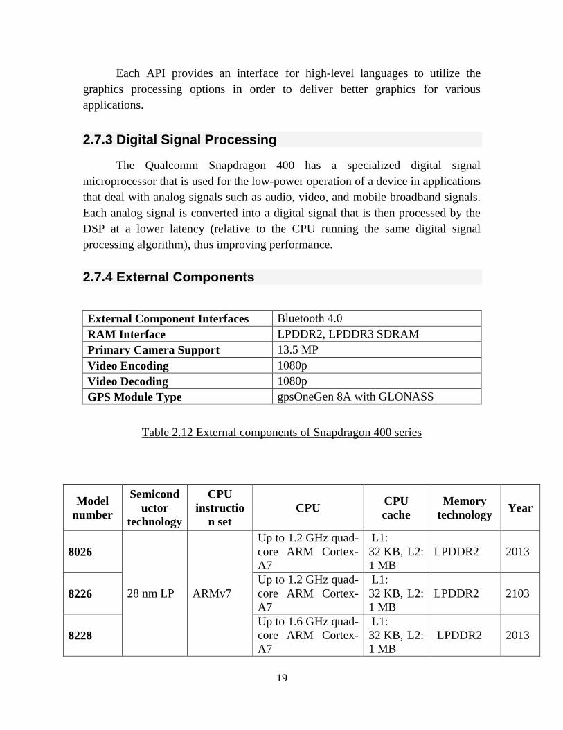
2.7.4 External Components
External Component Interfaces Bluetooth 4.0
RAM Interface LPDDR2, LPDDR3 SDRAM
Primary Camera Support 13.5 MP
Video Encoding 1080p
Video Decoding 1080p
GPS Module Type gpsOneGen 8A with GLONASS
Table 2.12 External components of Snapdragon 400 series
Model
number
Semicond
uctor
technology
CPU
instructio
n set
CPU CPU
cache
Memory
technology Year
8026
28 nm LP ARMv7
Up to 1.2 GHz quad-
core ARM Cortex-
A7
L1:
32 KB, L2:
1 MB
LPDDR2 2013
8226
Up to 1.2 GHz quad-
core ARM Cortex-
A7
L1:
32 KB, L2:
1 MB
LPDDR2 2103
8228
Up to 1.6 GHz quad-
core ARM Cortex-
A7
L1:
32 KB, L2:
1 MB
LPDDR2 2013
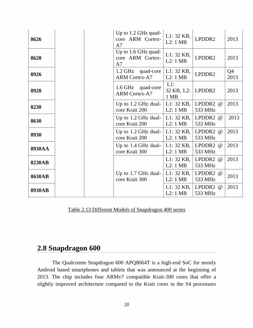
20
8626
Up to 1.2 GHz quad-
core ARM Cortex-
A7
L1: 32 KB,
L2: 1 MB LPDDR2 2013
8628
Up to 1.6 GHz quad-
core ARM Cortex-
A7
L1: 32 KB,
L2: 1 MB LPDDR2 2013
8926 1.2 GHz quad-core
ARM Cortex-A7
L1: 32 KB,
L2: 1 MB LPDDR2
Q4
2013
8928 1.6 GHz quad-core
ARM Cortex-A7
L1:
32 KB, L2:
1 MB
LPDDR2 2013
8230 Up to 1.2 GHz dual-
core Krait 200
L1: 32 KB,
L2: 1 MB
LPDDR2 @
533 MHz
2013
8630 Up to 1.2 GHz dual-
core Krait 200
L1: 32 KB,
L2: 1 MB
LPDDR2 @
533 MHz
2013
8930 Up to 1.2 GHz dual-
core Krait 200
L1: 32 KB,
L2: 1 MB
LPDDR2 @
533 MHz
2013
8930AA Up to 1.4 GHz dual-
core Krait 300
L1: 32 KB,
L2: 1 MB
LPDDR2 @
533 MHz
2013
8230AB
Up to 1.7 GHz dual-
core Krait 300
L1: 32 KB,
L2: 1 MB
LPDDR2 @
533 MHz
2013
8630AB L1: 32 KB,
L2: 1 MB
LPDDR2 @
533 MHz 2013
8930AB L1: 32 KB,
L2: 1 MB
LPDDR2 @
533 MHz
2013
Table 2.13 Different Models of Snapdragon 400 series
2.8 Snapdragon 600
The Qualcomm Snapdragon 600 APQ8064T is a high-end SoC for mostly
Android based smartphones and tablets that was announced at the beginning of
2013. The chip includes four ARMv7 compatible Krait-300 cores that offer a
slightly improved architecture compared to the Krait cores in the S4 processors
21
(according to Anandtech). However, the performance of Cortex-A15 cores should
not be reached, but the power consumption should be better.
2.8.1 Central Processing Unit
The Qualcomm Snapdragon 600 has a high performing CPU with a
maximum clock speed of 1,900.00 MHz. It has 4+4 core(s), resulting in extremely
efficient multi-tasking when compared to dual core processors.
As a result of following the Harvard architecture, the CPU has a separate
Level 1 instruction and data cache leading to a slight improvement in performance
over a unified Level 1 cache. The instruction cache is only used for storing
instructions and executes in a sequential manner. The data cache stores data used
by instructions; the point of access or storage is generally specified by an
instruction.
This processor is based on the Reduced Instruction Set Computing (RISC)
design strategy enabling instructions to execute faster, as opposed to the Complex
Instruction Set Computing (CISC) design strategy, which is generally slower at
executing due to lengthy instructions.
2.8.2 Graphics Processing Unit
The Qualcomm Adreno 320 is a separate graphics processor solely intended
for the accelerated creation of images to be outputted to a display. Its entire
architecture is structured around processing large blocks of data in parallel.
2.8.3 Digital Signal Processing
The Qualcomm Snapdragon 600 has a specialized digital signal
microprocessor that is used for the low-power operation of a device in applications
that deal with analog signals such as audio, video, and mobile broadband signals.
Each analog signal is converted into a digital signal that is then processed by the
DSP at a lower latency (relative to the CPU running the same digital signal
processing algorithm), thus improving performance. [3]
22
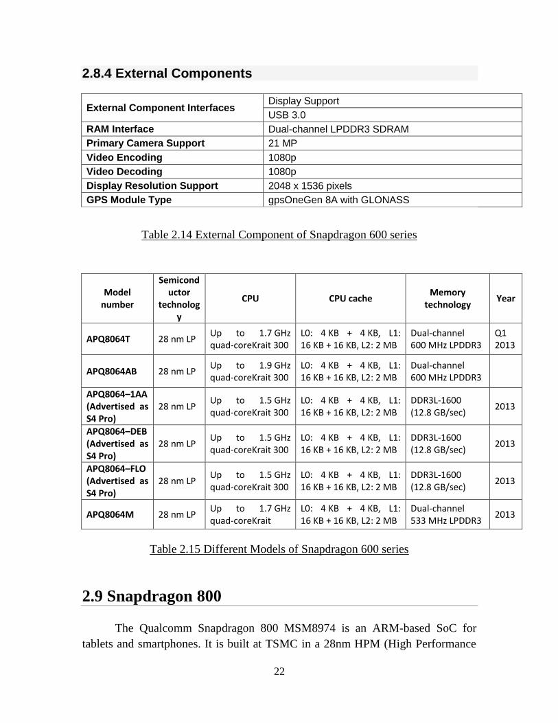
2.8.4 External Components
External Component Interfaces Display Support
USB 3.0
RAM Interface Dual-channel LPDDR3 SDRAM
Primary Camera Support 21 MP
Video Encoding 1080p
Video Decoding 1080p
Display Resolution Support 2048 x 1536 pixels
GPS Module Type gpsOneGen 8A with GLONASS
Table 2.14 External Component of Snapdragon 600 series
Model number
Semiconductor
technology
CPU CPU cache Memory
technology Year
APQ8064T 28 nm LP Up to 1.7 GHz quad-coreKrait 300
L0: 4 KB + 4 KB, L1: 16 KB + 16 KB, L2: 2 MB
Dual-channel 600 MHz LPDDR3
Q1 2013
APQ8064AB 28 nm LP Up to 1.9 GHz quad-coreKrait 300
L0: 4 KB + 4 KB, L1: 16 KB + 16 KB, L2: 2 MB
Dual-channel 600 MHz LPDDR3
APQ8064–1AA (Advertised as S4 Pro)
28 nm LP Up to 1.5 GHz quad-coreKrait 300
L0: 4 KB + 4 KB, L1: 16 KB + 16 KB, L2: 2 MB
DDR3L-1600 (12.8 GB/sec)
2013
APQ8064–DEB (Advertised as S4 Pro)
28 nm LP Up to 1.5 GHz quad-coreKrait 300
L0: 4 KB + 4 KB, L1: 16 KB + 16 KB, L2: 2 MB
DDR3L-1600 (12.8 GB/sec)
2013
APQ8064–FLO (Advertised as S4 Pro)
28 nm LP Up to 1.5 GHz quad-coreKrait 300
L0: 4 KB + 4 KB, L1: 16 KB + 16 KB, L2: 2 MB
DDR3L-1600 (12.8 GB/sec)
2013
APQ8064M 28 nm LP Up to 1.7 GHz quad-coreKrait
L0: 4 KB + 4 KB, L1: 16 KB + 16 KB, L2: 2 MB
Dual-channel 533 MHz LPDDR3
2013
Table 2.15 Different Models of Snapdragon 600 series
2.9 Snapdragon 800
The Qualcomm Snapdragon 800 MSM8974 is an ARM-based SoC for
tablets and smartphones. It is built at TSMC in a 28nm HPM (High Performance
23
Mobile) HKMG process, whereas the Snapdragon 600 was manufactured in 28nm
LP. In addition to 4 CPU cores with a clock speed of up to 2.3 GHz, the chip also
integrates an Adreno 330 GPU up to 450 MHz, an LPDDR3-1600 memory
controller and various radio modules.[6]
2.9.1 Central Processing Unit
The Qualcomm Snapdragon 800 MSM8074 has a high performing CPU
with a maximum clock speed of 2,300.00 MHz. It has 4 core(s), resulting
in extremely efficient multi-tasking when compared to dual core processors.
As a result of following the Harvard architecture, the CPU has a separate
Level 1 instruction and data cache leading to a slight improvement in performance
over a unified Level 1 cache. The instruction cache is only used for storing
instructions and executes in a sequential manner. The data cache stores data used
by instructions; the point of access or storage is generally specified by an
instruction.
This processor is based on the Reduced Instruction Set Computing (RISC)
design strategy enabling instructions to execute faster, as opposed to the Complex
Instruction Set Computing (CISC) design strategy, which is generally slower at
executing due to lengthy instructions.
2.9.2 Graphics Processing Unit
The Qualcomm Adreno 330 is a separate graphics processor solely intended
for the accelerated creation of images to be outputted to a display. Its entire
architecture is structured around processing large blocks of data in parallel.
Each API provides an interface for high-level languages to
utilize the graphics processing options in order to deliver better graphics for
various applications.
2.9.3 Digital Signal Processing
The Qualcomm Snapdragon 800 MSM8074 has a specialized digital signal
microprocessor that is used for the low-power operation of a device in applications
that deal with analog signals such as audio, video, and mobile broadband signals.

24
Each analog signal is converted into a digital signal that is then processed by the
DSP at a lower latency (relative to the CPU running the same digital signal
processing algorithm), thus improving performance.
2.9.4 External Components
External Component
Interfaces
USB 3.0
RAM Interface Dual-channel LPDDR3 SDRAM
Primary Camera Support 55 MP
Video Encoding 2160p
Video Decoding 2160p
GPS Module Type gpsOneGen 8B with GLONASS
Table 2.16 External components of Snapdragon 800 series
Technology Snapdragon 200
Series
Snapdragon 400
Series
Snapdragon 600
Series
Snapdragon 800
Series
Semiconductor 45 nm LP/28 nm LP 28 nm LP 28 nm LP 14 nm FinFET
Instruction set ARMv7 ARMv8 ARMv8 ARMv7/ARMv8A
CPU Speed Quad-core Up to 1.4
GHz
Up to 1.7 GHz
Octa-core
Up to 1.7 GHz
Quad-core
2.0 + 1.55 GHz
Quad-core
CPU Quad-core Cortex-A7 Octa-core
Cortex-A53
Dual-
core+Quad-core
Cortex-A53
4+4 cores Hydra
and Cortex
Cache Type L0,L1,L2 L1,L2 L0,L1,L2 L2
CPU Cache Up to 2 MB Up to 2 MB Up to 2 MB Up to 2 MB
GPU Adreno 304 Adreno 405 Adreno 510 Adreno 530
GPU Support WXGA/720p Up to FHD
1080p
Quad
HD2560x1600 4K UHD video
upscale

25
RAM
Technology LPDDR2/LPDDR3 533
MHz
LPDDR3 933
MHz
Dual-channel
LPDDR3
933 MHz
LPDDR4 1866
MHz
Bluetooth Bluetooth 4.1 Bluetooth 4.1 Bluetooth Smart
v4.1
Native Bluetooth
4.1 support
WiFi -
Multi-User
MIMO (MU-
MIMO) WiFi
VIVE 1-stream
802.11ac WiFi
802.11ac (2.4 and
5 GHz) WiFi
Table 2.17 Comparison between Snapdragon 200,400,600 & 800 series

26
CHAPTER-3
SNAPDRAGON PROCESSOR ARCHITECTURE
The Snapdragon central processing unit (CPU) uses the ARM RISC
instruction set, and a single SoC may include multiple CPU cores, a graphics
processing unit (GPU), a wireless modem, and other software and hardware to
support a smartphone's global positioning system (GPS), camera, gesture
recognition and video. Snapdragon semiconductors are embedded in most Google
Android and Windows Phone devices.
A Snapdragon Processor system on a chip or system on chip (SoC or SOC)
is an integrated circuit (IC) that integrates all components of a computer or other
electronic system into a single chip. It may contain digital, analog, mixed-signal,
and often radio-frequency functions—all on a single chip substrate.
3.1 Different components of Snapdragon processors
The Qualcomm Snapdragon processors, combines a processor cores,
Qualcomm's DSP and 4G LTE connectivity with ultra-low power consumption to
create new mobile devices which will revolutionize the world of mobile
computing. Snapdragon processor components are given below.
1. CPU (Central Processing Unit)
2. GPU (Graphics Processing Unit)
3. DSP (Digital Signal Processor)
4. Modem
5. System Security

27
Fig 3.1 Snapdragon processor block diagram
Fig 3.1 shows the different components of snapdragon processor. Mainly divided
into 7 blocks as follows Computing Engines, Cellular, Multimedia Engines,
System Security, Memory, Location and low Power Island.
3.2 CPU
A central processing unit (CPU) is the electronic circuitry within a system
that carries out the instructions of a program by performing the basic arithmetic,
logical, control and input/output (I/O) operations specified by the instructions. The
term has been used in the computer industry at least since the early 1960s
The Qualcomm Snapdragon 820 processor has been purposefully designed
to provide innovative user experiences for premium-tier mobile devices. To
deliver the type of innovation consumers expect, mobile processors must be
designed to handle increasing computing requirements, while simultaneously
using less battery power and remain cooler than ever, with thinner and lighter
designs being employed by OEMs.[8]
28
Experiences like virtual reality, computer vision, and advanced imaging are
helping expand smartphone capabilities, while also demanding more performance.
Balancing increased performance with longer battery life has always been critical
for mobile processors—and Snapdragon 820 has been designed with efficiency
throughout.
The 820 is engineered with custom-built, highly optimized cores designed
for heterogeneous computing—the ability to combine different functional cores of
the system-on-chip (SoC), like the CPU, GPU and DSP cores, to achieve
previously unattainable performance and power savings, rather than using the
same core for different tasks.
Qualcomm Technologies has been custom designing mobile processors for
over twenty-five years, and using our heterogeneous computing experience, we’ve
custom designed each of the individual cores of the Snapdragon 820 to achieve
higher efficiency so that they work together more effectively as a comprehensive
system with other onboard components, hence the term ―system-on-chip".[10]
3.2.1 Introducing Kryo
The CPU is still one of the most familiar cores on the modern SoC and is
key in setting the speed and heartbeat for the entire processor. With the
Snapdragon 820, Qualcomm Technologies is introducing Qualcomm Kryo, our
first custom-designed 64-bit quad-core CPU, as part of a comprehensive redesign
of our premium-tier mobile processor.
Kryo is tightly integrated with the Adreno 530 GPU and Hexagon 680
DSP and is designed for high-performance mobile computing along with the latest
in multimedia and connectivity. Kryo follows the popular custom Krait CPU,
which powers the Snapdragon 800, 801, and 805 processors.
3.2.2 Custom cores
Single computing component with two or more independent actual
processing units (called "cores"), which are the units that read and execute
program instructions. Custom cores for CPU to the Snapdragon processor because
customization means being able to meet the needs without compromising on
performance or battery life. Higher performance is often at odds with longer
battery life—but engineered into the first generation of Kryo.[11]
29
3.2.3 Symphony System Manager
Qualcomm Symphony System Manager because of the heterogeneous
nature of Snapdragon 820, increasingly more tasks are shared among the CPU,
GPU, and DSP, as well as with special purpose components such as the
Qualcomm Spectra camera ISP. That means even more system performance and
power savings can be achieved, when you can run the right task on the right
processor, or properly combine the right processors together for the right task.
While some processors limit their system management to CPU cores,
Symphony is designed to manage the entire system-on-chip in different
configurations so that the most efficient and effective combination of processors
and specialized cores are chosen to get the job done as quickly as possible, with
the least amount of power. For example, when a user is taking a picture,
Symphony responds to the system demand making sure that the right components
are powered up running at the needed frequency and only as long as needed. These
components include CPU, Spectra ISP, Snapdragon Display Engine, GPU, GPS,
and memory system.
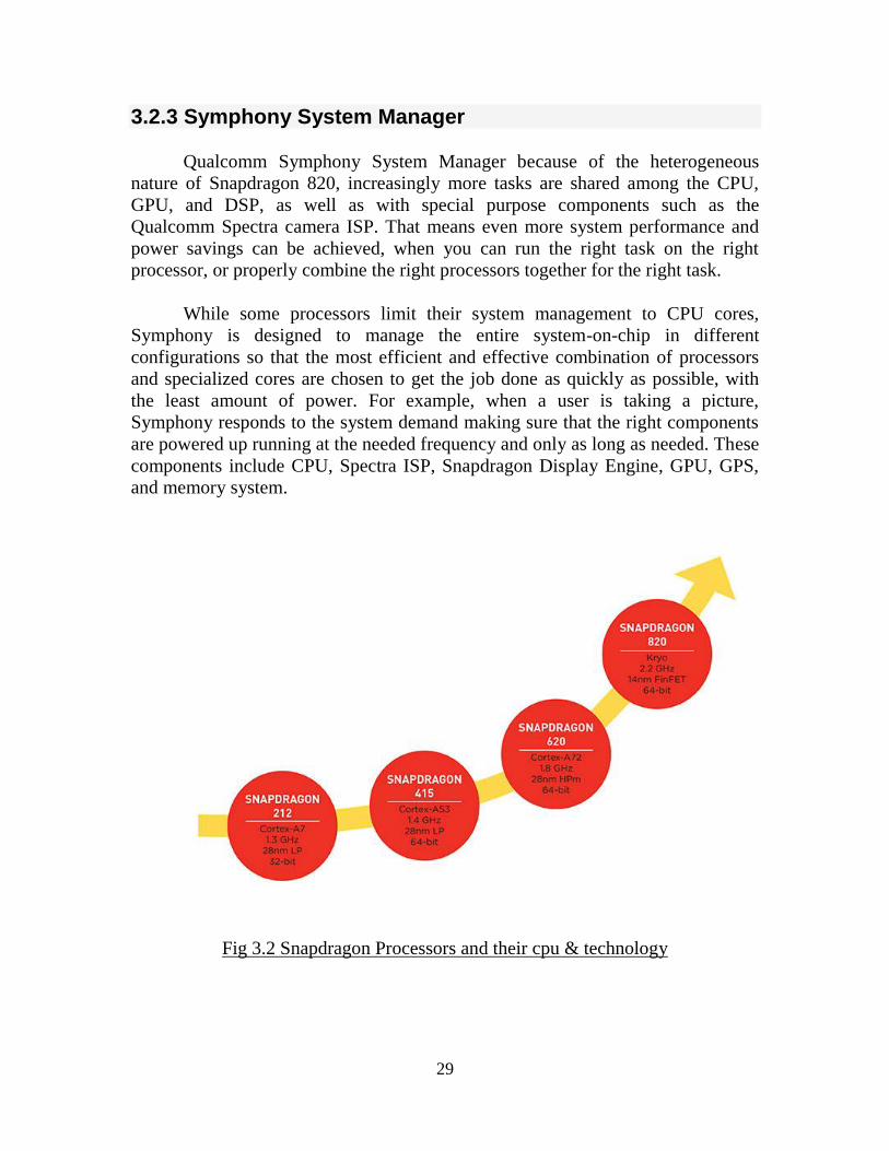
Fig 3.2 Snapdragon Processors and their cpu & technology
30
Fig: The higher the Snapdragon tier, the higher the performance and the
faster the speeds
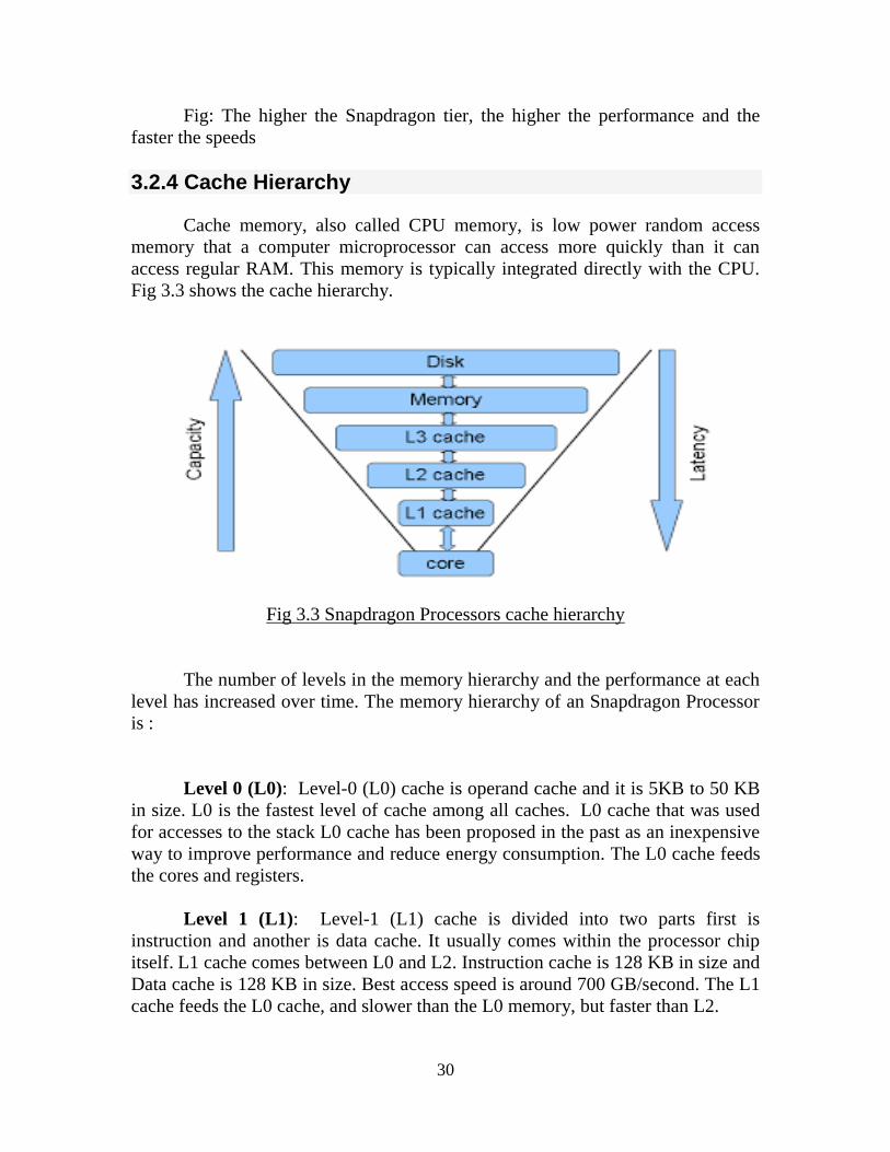
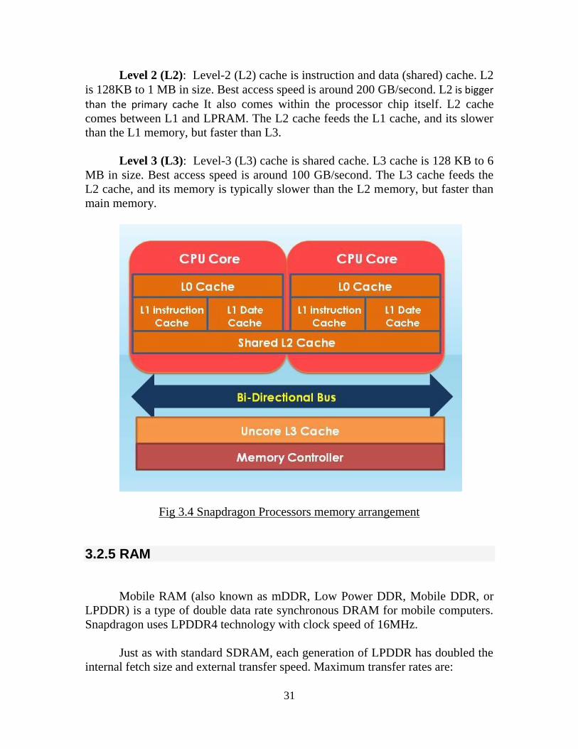
3.2.4 Cache Hierarchy
Cache memory, also called CPU memory, is low power random access
memory that a computer microprocessor can access more quickly than it can
access regular RAM. This memory is typically integrated directly with the CPU.
Fig 3.3 shows the cache hierarchy.
Fig 3.3 Snapdragon Processors cache hierarchy
The number of levels in the memory hierarchy and the performance at each
level has increased over time. The memory hierarchy of an Snapdragon Processor
is :
Level 0 (L0): Level-0 (L0) cache is operand cache and it is 5KB to 50 KB
in size. L0 is the fastest level of cache among all caches. L0 cache that was used
for accesses to the stack L0 cache has been proposed in the past as an inexpensive
way to improve performance and reduce energy consumption. The L0 cache feeds
the cores and registers.
Level 1 (L1): Level-1 (L1) cache is divided into two parts first is
instruction and another is data cache. It usually comes within the processor chip
itself. L1 cache comes between L0 and L2. Instruction cache is 128 KB in size and
Data cache is 128 KB in size. Best access speed is around 700 GB/second. The L1
cache feeds the L0 cache, and slower than the L0 memory, but faster than L2.
31
Level 2 (L2): Level-2 (L2) cache is instruction and data (shared) cache. L2
is 128KB to 1 MB in size. Best access speed is around 200 GB/second. L2 is bigger
than the primary cache It also comes within the processor chip itself. L2 cache
comes between L1 and LPRAM. The L2 cache feeds the L1 cache, and its slower
than the L1 memory, but faster than L3.
Level 3 (L3): Level-3 (L3) cache is shared cache. L3 cache is 128 KB to 6
MB in size. Best access speed is around 100 GB/second. The L3 cache feeds the
L2 cache, and its memory is typically slower than the L2 memory, but faster than
main memory.
Fig 3.4 Snapdragon Processors memory arrangement
3.2.5 RAM
Mobile RAM (also known as mDDR, Low Power DDR, Mobile DDR, or
LPDDR) is a type of double data rate synchronous DRAM for mobile computers.
Snapdragon uses LPDDR4 technology with clock speed of 16MHz.
Just as with standard SDRAM, each generation of LPDDR has doubled the
internal fetch size and external transfer speed. Maximum transfer rates are:

32
LPDDR generations
LPDDR1 LPDDR2 LPDDR3 LPDDR4
Internal access rate 200 MHz 200 MHz 200 MHz 200 MHz
Prefetch size 2n 4n 8n 16n
Clock frequency 200 MHz 400 MHz 800 MHz 1600 MHz
Data transfer rate
(DDR) 400 MT/s 800 MT/s 1600 MT/s 3200 MT/s
Supply voltage(s) 1.8 V 1.2 V, 1.8
V 1.2 V, 1.8 V 1.1 V, 1.8 V
Command/
Address bus
19 bits,
SDR
10 bits,
DDR
10 bits,
DDR 6 bits, SDR
Table 3.1 Comparison between LPDDR1, LPDDR2, LPDDR3 & LPDDR4
3.3 GPU
GPUs are an essential part of those chipsets and as mobile games are
pushing the boundaries of their capabilities, the GPU performance is becoming
increasingly important. A graphics processing unit (GPU), also occasionally called
visual processing unit (VPU), is a specialized electronic circuit designed to rapidly
manipulate and alter memory to accelerate the creation of images in a frame buffer
intended for output to a display.
Qualcomm Technologies introduced our next-generation visual processing
technologies with the latest versions of the Qualcomm Adreno GPU and
Qualcomm Spectra camera ISP (image signal processor) to bring significant
performance, power efficiency, and user experience advances to upcoming
Qualcomm Snapdragon processors.
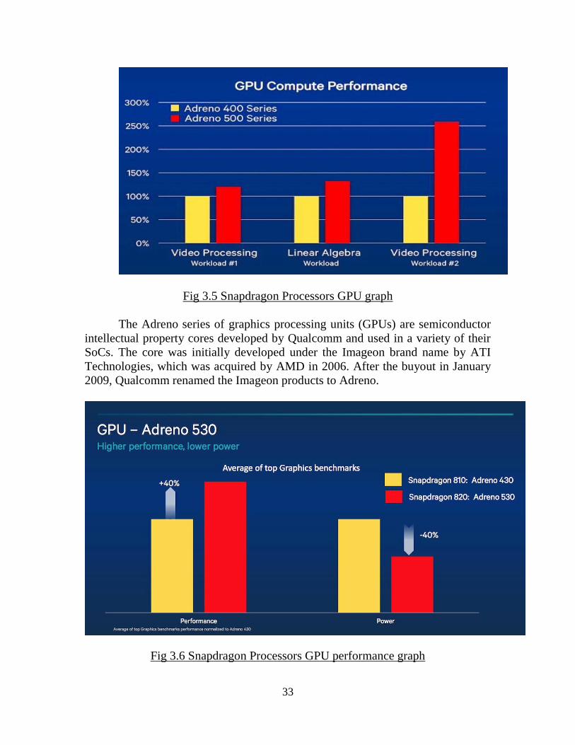
Fig. 3.5 & Fig 3.6 shows the comparison between Adreno 400 and Adreno
500 series
33
Fig 3.5 Snapdragon Processors GPU graph
The Adreno series of graphics processing units (GPUs) are semiconductor
intellectual property cores developed by Qualcomm and used in a variety of their
SoCs. The core was initially developed under the Imageon brand name by ATI
Technologies, which was acquired by AMD in 2006. After the buyout in January
2009, Qualcomm renamed the Imageon products to Adreno.
Fig 3.6 Snapdragon Processors GPU performance graph

34
3.4 DSP (Digital Signal Processor)
Qualcomm Technologies developed the Hexagon Digital Signal Processor
(DSP) as a world class processor with both CPU and DSP functionality to support
deeply embedded processing needs of the mobile platform for both multimedia
and modem functions. It is an advanced, variable instruction length, Very Long
Instruction Word (VLIW) processor architecture with hardware multi -threading.
The Hexagon architecture and family of cores provides Qualcomm Technologies a
competitive advantage in performance and power efficiency for modem and multi-
media applications and is a key component of all of Qualcomm’s Snapdragon
processors. [9] Fig 3.7 shows the threading of DSP.
Fig 3.7 Snapdragon Processors DSP threading
All instructions operate on a shared 32-entry per-thread register file. Vector
operations use register pairs from the general register file. The ISA features a rich
set of DSP arithmetic support including 16-bit and 32-bit fractional and complex
data types, 32-bit floating-point and full 64-bit integer arithmetic support.
There are two main new features to the Hexagon 680. The first is a
completely separate DSP for sensor processing. The aptly named ―low power
island‖ is designed to improve the battery life of always-on use cases, including
step or activity counters as well as sensor-assisted positioning (using your phones’
sensors to provide more accurate location when you don’t have a strong GPS
signal).

35
Snapdragon
generation
DSP Frequency,
MHz
Process
node, nm
S1 600 65
S2 256 45
S3 400 45
S4 500 28
S4 500 28
S4 500 28
S200 384 45 LP
S400 500 28 LP
S600 500 28 LP
S800 600 28 HPm
Table 3.2 Snapdragon DSP frequency
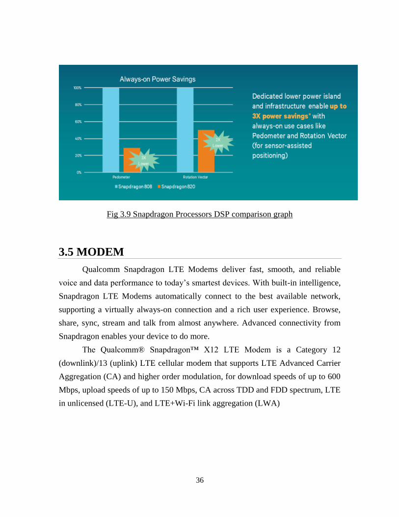
The second feature brings a new level of horsepower to Hexagon in the
form of HVX (Hexagon Vector eXtensions). This added hardware supports
advanced imaging and computer vision when paired with the Qualcomm Spectra
camera ISP. For example, in low-light situations, the Snapdragon 820 will use the
ISP and DSP to adaptively brighten areas of both video and photos that would
otherwise appear too dark. With Hexagon 680, the Snapdragon 820 is engineered
to perform this action several times faster and at only 10% of the power. [9] Fig
3.8 shows the comparison b/w different DSP and Fig 3.9 shows lesser power
consumption.
Fig 3.8 Snapdragon Processors DSP performance graph
36
Fig 3.9 Snapdragon Processors DSP comparison graph
3.5 MODEM
Qualcomm Snapdragon LTE Modems deliver fast, smooth, and reliable
voice and data performance to today’s smartest devices. With built-in intelligence,
Snapdragon LTE Modems automatically connect to the best available network,
supporting a virtually always-on connection and a rich user experience. Browse,
share, sync, stream and talk from almost anywhere. Advanced connectivity from
Snapdragon enables your device to do more.
The Qualcomm® Snapdragon™ X12 LTE Modem is a Category 12
(downlink)/13 (uplink) LTE cellular modem that supports LTE Advanced Carrier
Aggregation (CA) and higher order modulation, for download speeds of up to 600
Mbps, upload speeds of up to 150 Mbps, CA across TDD and FDD spectrum, LTE
in unlicensed (LTE-U), and LTE+Wi-Fi link aggregation (LWA)

37
Fig 3.10 Snapdragon Processors higher order modulation
Fig. 3.10 shows higher order of modulation.X12 LTE Modem is the first
commercially announced mobile processor to support:
LTE Category 12 downloads speeds of up to 600 Mbps: Yes, 600 Mbps — as
in ―we just passed the half-a-gigabit mark.‖ That’s a full 33 percent faster than the
peak download speeds of the X10 LTE modem in the Snapdragon 810, which
supported up to Cat 9 (450 Mbps). Why? Because you’ve got big files to
download from cloud storage, an Instagram feed to peruse, and high resolution
videos to stream. And we want to help you do it all faster and smoother.
LTE Category 13 uplink speeds of up to 150 Mbps : That’s triple the peak upload
speeds supported by X10 LTE in the Snapdragon 810. Triple. Why? Because
Snapdragon 820 is designed to help you take amazing pictures and videos, and we
want to help you share them even faster with your friends and family. And
because you need high uplink bandwidth to look your best in your next Periscope
broadcast.

38
LTE in Unlicensed (LTE-U): Increasing mobile network capacity and user
throughput by aggregating LTE in licensed and unlicensed bands.
Antenna sharing: The X12 supports several antenna sharing schemes between
LTE and Wi-Fi, designed to make it easier for manufacturers to design devices
with advanced technologies like LTE-U, 4x4 LTE MIMO, and 2-stream Wi-Fi,
with attractive form factors and minimal performance impact on either technology.
3.6 System Security
Security is most important issue in these days. Today's mobile users need
more robust security to address ever-increasing threats to device security and
privacy. And they need that in the form of power-efficient solutions that don’t
interfere with the use of their devices. The Qualcomm® Haven™ Security
Solutions suite is designed to provide exactly that: a robust, multidimensional suite
of mobile security technologies, engineered for performance and efficiency in
today's complex mobile environment.
Fig 3.11 Snapdragon Processors security module
39
Why Snapdragon Smart Protect?
End-users and enterprises, along with their devices and data, are under
increasing attack from mobile malware. Thousands of new mobile malware apps
are generated each day. And traditional, signature-based anti-malware apps alone
aren't able to detect and stop all of them.
Personal Protection
Snapdragon Smart Protect is engineered to support robust security and
enhanced personal privacy for today's mobile environment, empowering users
with greater control over their personal data by detecting and classifying a broader
range of spyware, adware and other malicious app behavior.
Superior Behavioral-based detection
Most anti-malware solutions catch malware by matching the signature file
of an already-known malware app to a file in their database. Snapdragon Smart
Protect uses Qualcomm® Zeroth™ cognitive computing technology within the
Qualcomm® Snapdragon™ 820 processor to look at actual, real-time application
behavior to almost instantly detect suspicious behavior from even the newest or
"zero-day" malware.
Snapdragon Smart Protect is designed to enable OEMs and mobile security
solution providers to enhance traditional anti-malware and privacy protection
services with real-time, behavioral-based machine learning. Snapdragon Smart
Protect is engineered to complement existing signature-based anti-malware
solutions by analyzing and detecting new threats before the signature files of these
malicious applications have been incorporated into anti-malware application
databases. Snapdragon Smart Protect also is designed to classify detected malware
according to level of severity and offer specific reasons why a particular process
or behavior was detected as suspicious.
Power-efficient performance
Snapdragon Smart Protect is made to offer optimal performance through
on-device design and uniquely deep access to the hardware and software of the

40
Snapdragon 820 processor, supporting malware detection and critical data
processing on the device, rather than in the cloud. By doing behavioral analysis on
the device, Snapdragon Smart Protect is designed to detect and classify new and
transformed malware quickly and efficiently.[4]

41
CHAPTER-4
SNAPDRAGON PROCESSOR TECHNOLOGY
Qualcomm Snapdragon Processors are latest in technology there are
various smart technologies used which make it smarter than other and efficient in
terms of power consumption. These are given below :
1. Semiconductor Technology
2. Instruction Set
4.1 Semiconductor Technology
Semiconductor Technology is actually semiconductor device fabrication.
Semiconductor device fabrication is the process used to create the integrated
circuits. It is a multiple-step sequence of photo lithographic and chemical
processing steps during which electronic circuits are gradually created on a wafer
made of pure semiconducting material. Silicon is almost always used, but various
compound semiconductors are used for specialized applications.
4.1.1 65nm semiconductor technology
The 65 nanometer (65 nm) process is advanced lithographic node used in
volume CMOS semiconductor fabrication. Printed linewidths (i.e., transistor gate
lengths) can reach as low as 25 nm on a nominally 65 nm process, while the pitch
between two lines may be greater than 130 nm.

42
Fig 4.1 Snapdragon Processors 65nm technology
Example: 65 nm process
Gate length: 30 nm (high-performance) to 50 nm (low-power)
Core voltage: 1.0 V
11 Cu interconnect layers using nano-clustering silica as ultralow k
dielectric (k=2.25)
Metal 1 pitch: 180 nm
Nickel silicide source/drain
Gate oxide thickness: 1.9 nm (n), 2.1 nm (p)
Some Snapdragon Processor S1 are using 65 nm manufacturing technology
4.1.2 45nm semiconductor technology
45 nanometer (45 nm) technology node should refer to the average half-
pitch of a memory cell manufactured at around the 2007–2008 time frame. Many
critical feature sizes are smaller than the wavelength of light used for lithography
(i.e., 193 nm and 248 nm). A variety of techniques, such as larger lenses, are used
to make sub-wavelength features

43
Fig 4.2 Snapdragon Processors 45nm technology
Example: 45nm process
160 nm gate pitch (73% of 65 nm generation)
200 nm isolation pitch (91% of 65 nm generation) indicating a slowing of
scaling of isolation distance between transistors
Extensive use of dummy copper metal and dummy gates
35 nm gate length (same as 65 nm generation)
1 nm equivalent oxide thickness, with 0.7 nm transition layer
Gate-last process using dummy polysilicon and damascene metal gate
Squaring of gate ends using a second photoresist coating
9 layers of carbon-doped oxide and Cu interconnect, the last being a thick
"redistribution" layer
Contacts shaped more like rectangles than circles for local interconnection
Lead-free packaging
1.36 mA/um nFET drive current
1.07 mA/um pFET drive current, 51% faster than 65 nm generation, with
higher hole mobility due to increase from 23% to 30% Ge in embedded SiGe
stressors

44
Some Snapdragon Processor S1, Snapdragon Processor S2, Snapdragon Processor
S3, Snapdragon Processor S4 and Snapdragon Processor 200 series are using 45
nm manufacturing technology.[4]
4.1.3 28nm LP semiconductor technology
The 28nm generation represents most energy-efficient and high-
performance method of manufacturing to date. 28nm is the first generation that
foundry industry starts to use high-K metal gate (HKMG) process. The 28nm High
Performance Mobile Computing (HPM) provides high performance for mobile
applications to address the need for applications requiring high speed. Such
technology can provide the highest speed among 28nm technologies. With such
higher performance coverage, 28HPM is ideal for many applications from
networking, and high-end Smartphone/ mobile consumer products.[14]
Some Snapdragon Processor S4, Snapdragon Processor 200 series,
Snapdragon Processor 400 series, Snapdragon Processor 600 series and
Snapdragon Processor 800 series are using 28 nm manufacturing technology
4.1.4 14 nm FinFET semiconductor technology
The 14 nanometer (14 nm) semiconductor device fabrication node is the
technology node following the 22 nm/(20 nm) node. The naming of this
technology node as "14 nm" came from the International Technology Roadmap for
Semiconductors (ITRS). A 14nm FinFET design combines the optimized area and
performance boost required for next-generation platforms while also ensuring very
low power dissipation.
FinFET, also known as Fin Field Effect Transistor, is a type of non-planar
or "3D"transistor used in the design of modern processors. As in earlier, planar
designs, it is built on an SOI (silicon on insulator) substrate. However, FinFET
designs also use a conducting channel that rises above the level of the insulator,

45
creating a thin silicon structure, shaped like a fin, which is called agate electrode.
This fin-shaped electrode allows multiple gates to operate on a single transistor.[4]
14LPE – Early time-to-market version with area and power benefits for mobility
applications
14LPP – Enhanced version with higher performance and lower power; a full
platform offering with MPW, IP enablement and wide application coverage
Fig 4.3 Snapdragon Processors 14nm technology
4.2 Instruction Set
An instruction set, or instruction set architecture (ISA), is the part of the
computer architecture related to programming, including the native data
types, instructions, registers, addressing modes, memory architecture, interrupt
and exception handling, and external I/O.

46
Snapdragon uses following instruction sets
1. ARMv6
2. ARMv7
3. ARMv8
4.2.1 ARMv6
ARMv6 is aimed at the very low end of the 32-bit microcontroller space,
enabling very low gate-count designs with very simple and highly efficient micro
architecture. Several features of ARMv7 are not available to enable this simplicity.
The following is a summary of the major changes:
The ARMv6 instruction set is the smallest supported by any ARM processors,
numbering just 57 distinct instructions. With the exception of 6 OS-type
instructions, all are 16-bit.
Privileged execution is an implementation-option (meaning that it may be
included or excluded from the device during the chip design process). This is
referred to as the ―Unprivileged/Privileged Extension‖
The SysTick timer is an implementation-option.
The maximum number of external interrupts is limited to 32 and only four
priority levels are available.
Halting debug support is optional.
Memory accesses must always be naturally aligned.
Exclusive accesses are not supported.
The Memory Protection Unit is available as an implementation-option (the
PMSA Extension). It is currently supported only by the Cortex-M0+.

47
4.2.2 ARMv7
This generation introduced the Thumb 16-bit instruction set providing
improved code density compared to previous designs. The most widely used
ARM7 designs implement the ARMv4T architecture. All these designs use Von
Neumann architecture, thus the few versions comprising a cache do not separate
data and instruction caches. The processor supports both 32-bit and 16-bit
instructions via the ARM and Thumb instruction sets.[12]
The following is a summary of the major changes:
Higher Instructions per cycle
New and more complex instruction sets are added
Additional cache memory compare to previous model
A Thumb-2 extension is used.
Armv7 architecture has a "NEON" unit that provides blindingly fast
hardware support for single precision floating point arithmetic
ARMv6 ARMv7
1 Lower IPC((instructions per
clocks) 1 Higher IPC
2 Less instructions 2 More complex instruction sets
3 Old design 3 New deisgn
4 Less cache memory 4 More cache memory
5 Thumb-1 extensions 5 Thumb-2 extensions
6
Architecture has hardware support
for double precision floating point
arithmetic
6
Armv7 architecture has a "NEON" unit that
provides blindingly fast hardware support
for single precision floating point arithmetic
Table 4.1 Comparison between ARMv6 & ARMv7

48
4.2.3 ARMv8
The ARMv8 architecture introduces 64-bit support to the ARM architecture
with a focus on power-efficient implementation while maintaining compatibility
with existing 32-bit software. By adopting a clean approach ARMv8-A processors
extend the performance range available while maintaining the low power
consumption characteristics of the ARM processors that will power tomorrow's
most innovative and efficient devices.
ARMv8-A introduces 64-bit architecture support to the ARM architecture
and includes:
64-bit general purpose registers, SP (stack pointer) and PC (program counter)
64-bit data processing and extended virtual addressing
Two main execution states:
AArch64 - The 64-bit execution state including exception model, memory
model, programmers' model and instruction set support for that state
AArch32 - The 32-bit execution state including exception model, memory
model, programmers' model and instruction set support for that state
The execution states support three key instruction sets:
A32 (or ARM): a 32-bit fixed length instruction set, enhanced through the
different architecture variants. Part of the 32-bit architecture execution
environment now referred to as AArch32.
T32 (Thumb) introduced as a 16-bit fixed-length instruction set,
subsequently enhanced to a mixed-length 16- and 32-bit instruction set on the
introduction of Thumb-2 technology. Part of the 32-bit architecture execution
environment now referred to as AArch32.
A64 is a 64-bit fixed-length instruction set that offers similar functionality
to the ARM and Thumb instruction sets. Introduced with ARMv8-A, it is the
AArch64 instruction set.[13]

49
SN ARMv7 ARMv8
1 Full supports both 32-bit and 16-bit
instructions, not support for 64-bit
Full native 32-bit execution, side-by-side
with 64-bit
2 Old 32-bit architecture New, modern, A64 instruction set
architecture (ISA)
3 only regular registers are available Double the number (and size) of registers
4 instructions for 16-bit and 32-bit New instructions for both A32 and A64
5 complex instruction set Cleaner instruction set architecture
6 no acceleration is available Up to 16x crypto acceleration
7 not support for big.LITTLE technology Fits well with big.LITTLE technology
8 supports thumb-2 T32 thumb is introduced
Table 4.2 Comparison between ARMv7 & ARMv8