quad network power controller for power-over-lan · the max5935 quad network power controller is...
TRANSCRIPT

General DescriptionThe MAX5935 quad network power controller is designedfor use in IEEE 802.3af-compliant power sourcing equip-ment (PSE). The device provides power devices (PD) dis-covery, classification, current limit, and both DC and ACload disconnect detections. The MAX5935 can be usedin either endpoint PSE (LAN switches/routers) or midspanPSE (power injector) applications.
The MAX5935 can operate autonomously or be con-trolled by software through an I2C-compatible interface.Separate input and output data lines (SDAIN andSDAOUT) allow usage with optocouplers. TheMAX5935 is a slave device. Its four address inputsallow 16 unique MAX5935 addresses. A separate INToutput and four independent shutdown inputs (SHD_)allow fast response from a fault to port shutdown. ARESET input allows hardware reset of the device. Aspecial Watchdog feature allows the hardware togracefully take over control if the software crashes. Acadence timing feature allows the MAX5935 to be usedin midspan systems.
The MAX5935 is fully software configurable and program-mable. A class-over-current detection function enablessystem power management to detect if a PD draws morecurrent than the allowable amount for its class. Other fea-tures are input under/overvoltage lockout, overtempera-ture protection, output voltage slew-rate limit duringstartup, power-good, and fault status. The MAX5935’sprogrammability includes gate charging current, current-limit threshold, startup timeout, overcurrent timeout,autorestart duty cycle, PD disconnect AC detectionthreshold, and PD disconnect detection timeout.
The MAX5935 is available in a 36-pin SSOP packageand is rated for both extended (-40°C to +85°C) andcommercial (0°C to +70°C) temperature ranges.
ApplicationsPower-Sourcing Equipment (PSE)
Power-Over-LAN/Power-Over-Ethernet
Switches/Routers
Midspan Power Injectors
Features♦ IEEE 802.3af Compliant♦ Controls Four Independent, -48V-Powered
Ethernet Ports in Either Endpoint or Midspan PSEApplications
♦ Wide Digital Power Input, VDIG, Common-ModeRange: VEE to (AGND + 7.7V)
♦ PD Violation of Class Current Protection♦ PD Detection and Classification♦ Provides Both DC and AC Load Removal
Detections♦ I2C-Compatible, 3-Wire Serial Interface♦ Fully Programmable and Configurable Operation
Through I2C Interface♦ Current Foldback and Duty-Cycle-
Controlled/Programmable Current Limit♦ Short-Circuit Protection with Fast Gate Pulldown♦ Direct Fast Shutdown Control Capability♦ Programmable Direct Interrupt Output♦ Watchdog Mode Enable Hardware Graceful
Takeover
MA
X5
93
5
Quad Network Power Controllerfor Power-Over-LAN
________________________________________________________________ Maxim Integrated Products 1
36
35
34
33
32
31
30
29
28
27
26
25
24
23
1
2
3
4
5
6
7
8
9
10
11
12
13
14
OSC_IN
AUTO
OUT1
GATE1
SENSE1
OUT2
GATE4
GATE2
SENSE2
VEE
OUT3
GATE3
SENSE3
OUT4
DET4
DET3
DET2
DET1
A0
A1
A2
A3
SDAIN
SDAOUT
SCL
MIDSPAN
SSOP
TOP VIEW
MAX5935
22
21
20
19
15
16
17
18
SENSE4
AGNDVDD
DGND
RESET
INT
SHD1
SHD2 SHD3
SHD4
Pin Configuration
19-3412; Rev 3; 5/07
For pricing, delivery, and ordering information, please contact Maxim/Dallas Direct! at 1-888-629-4642, or visit Maxim’s website at www.maxim-ic.com.
Ordering Information
PART TEMP RANGE PIN-PACKAGEPKG
CODE
MAX5935CAX 0°C to +70°C 36 SSOP A36-2
MAX5935CAX+ 0°C to +70°C 36 SSOP A36-2
MAX5935EAX -40°C to +85°C 36 SSOP A36-2
MAX5935EAX+ -40°C to +85°C 36 SSOP A36-2
Typical Operating Circuits appear at end of data sheet.

MA
X5
93
5
Quad Network Power Controllerfor Power-Over-LAN
2 _______________________________________________________________________________________
ABSOLUTE MAXIMUM RATINGS
Stresses beyond those listed under “Absolute Maximum Ratings” may cause permanent damage to the device. These are stress ratings only, and functionaloperation of the device at these or any other conditions beyond those indicated in the operational sections of the specifications is not implied. Exposure toabsolute maximum rating conditions for extended periods may affect device reliability.
(Voltages referenced to VEE, unless otherwise noted.)AGND, DGND, DET_, VDD, RESET, A3, A2, A1, A0, SHD_,
OSC_IN, SCL, SDAIN, OUT_ and AUTO............-0.3V to +80VGATE_ (Internally Clamped, Note 1) ...................-0.3V to +11.4VSENSE_ ..................................................................-0.3V to +24VVDD, RESET, A3, A2, A1, A0, SHD_, OSC_IN, SCL, SDAIN and
AUTO to DGND ....................................................-0.3V to +7VINT and SDAOUT to DGND....................................-0.3V to +12VMaximum Current into INT, SDAOUT, DET_ .......................80mA
Maximum Power Dissipation36-Pin SSOP (derate 11.4mW/°C above +70°C) .........941mW
Operating Temperature Ranges:MAX5935EAX ..................................................-40°C to +85°CMAX5935CAX .....................................................0°C to +70°C
Storage Temperature Range .............................-65°C to +150°CJunction Temperature ......................................................+150°CLead Temperature (soldering, 10s) .................................+300°C
ELECTRICAL CHARACTERISTICS(AGND = +48V. VEE = 0V, VDD to DGND = +3.3V. All voltages are referenced to VEE, unless otherwise noted. Typical values are at AGND = +48V, DGND = +48V, VDD = (DGND + 3.3V), TA = +25°C. Currents are positive when entering the pin andnegative otherwise.)
PARAMETER SYMBOL CONDITIONS MIN TYP MAX UNITS
POWER SUPPLIES
VAGND VAGND - VEE 32 60
VDGND 0 60
VDD to VDGND, VDGND = VAGND 1.71 5.50Operating Voltage Range
VDDVDD to VDGND, VDGND = VEE 3.0 5.5
V
IEE
OUT_= VEE, SENSE_ = VEE, DET_ = AGND,all logic inputs open, SCL = SDAIN = VDD,INT and SDAOUT open; measured at AGNDin power mode after GATE_ pullup
4.2 6.8Supply Currents
IDIG All logic inputs high, measured at VDD 2.7 5.6
mA
GATE DRIVER AND CLAMPING
GATE_ Pullup Current IPU Power mode, gate drive-on, VGATE = VEE (Note 2) -35 -50 -65 µA
Weak GATE_ Pulldown Current IPDW SHD_ = DGND, VGATE_ = VEE + 5V 25 40 55 µA
Maximum Pulldown Current IPDS VSENSE = 1V, VGATE_ = VEE + 2V 100 mA
External Gate Drive VGS VGATE - VEE , power mode, gate drive-on 9 10 11 V
CURRENT LIMIT
Current-Limit Clamp Voltage VSU_LIMMaximum VSENSE_ allowed during current limit,VOUT_ = VEE (Note 3)
202 212 222 mV
Default, Class 0,Class 3, Class 4
177 196
Class 1 48 61Overcurrent Threshold AfterStartup
VFLT_LIM
Overcurrent VSENSE_threshold allowed fort ≤ tFAULT after startup;VOUT_ = VEE Class 2 89 105
mV
Foldback Initial OUT_ Voltage VFLBK_STVOUT_ - VEE, above which the current-limit tripvoltage starts folding back
30 V
Foldback Final OUT_ Voltage VFLBK_ENDVOUT_ - VEE, above which the current-limit tripvoltage reaches VTH_FB
50 V

MA
X5
93
5
Quad Network Power Controllerfor Power-Over-LAN
_______________________________________________________________________________________ 3
ELECTRICAL CHARACTERISTICS (continued)(AGND = +48V. VEE = 0V, VDD to DGND = +3.3V. All voltages are referenced to VEE, unless otherwise noted. Typical values are at AGND = +48V, DGND = +48V, VDD = (DGND + 3.3V), TA = +25°C. Currents are positive when entering the pin andnegative otherwise.)
PARAMETER SYMBOL CONDITIONS MIN TYP MAX UNITS
Minimum Foldback Current-Limit Threshold
VTH_FB VOUT_ = VAGND 64 mV
SENSE_ Input Bias Current VSENSE_ = VEE -2 µA
SUPPLY MONITORS
VEE Undervoltage Lockout VEEUVLO VAGND - VEE, (VAGND – VEE) increasing 28.5 V
VEE Undervoltage-LockoutHysteresis
VEEUVLOH 3 V
VEE Overvoltage VEE_OV (VAGND - VEE) > VEE_OV, VAGND increasing 62.5 V
VEE Overvoltage Hysteresis VOVH 1 V
VEE Undervoltage VEE_UV (VAGND - VEE) < VEE_UV, VAGND decreasing 40 V
VDD Overvoltage VDD_OV (VDD - VDGND) > VDD_OV, VDD increasing 3.71 V
VDD Undervoltage VDD_UV (VDD - VDGND) < VDD_UV, VDD decreasing 2.82 V
VDD Undervoltage Lockout VDDUVLODevice operates when (VDD - VDGND) >VDDUVLO, VDD increasing
1.3 V
VDD Undervoltage-LockoutHysteresis
VDDHYS 120 mV
Thermal-Shutdown Threshold TSHD
Ports shut down and device resets if its junctiontemperature exceeds this limit, temperatureincreasing
+150 °C
Thermal-Shutdown Hysteresis TSHDH 20 °C
OUTPUT MONITOR
OUT_ Input Current IBOUT VOUT = VAGND, all modes 2 µA
Idle Pullup Current at OUT_ IDIS
OUT_ discharge current, detection andclassification off, port shutdown,VOUT_ = VAGND - 2.8V
200 260 µA
PGOOD High Threshold PGTH VOUT_ - VEE, OUT_ decreasing 1.5 2.0 2.5 V
PGOOD Hysteresis PGHYS 220 mV
PGOOD Low-to-High GlitchFilter
tPGOODMinimum time PGOOD has to be high to set bit inregister 10h
3 ms
LOAD DISCONNECT
DC Load DisconnectThreshold
VDCTHMinimum VSENSE allowed before disconnect (DCdisconnect active), VOUT_ = VEE
2.5 4 5 mV

MA
X5
93
5
Quad Network Power Controllerfor Power-Over-LAN
4 _______________________________________________________________________________________
ELECTRICAL CHARACTERISTICS (continued)(AGND = +48V. VEE = 0V, VDD to DGND = +3.3V. All voltages are referenced to VEE, unless otherwise noted. Typical values are at AGND = +48V, DGND = +48V, VDD = (DGND + 3.3V), TA = +25°C. Currents are positive when entering the pin andnegative otherwise.)
PARAMETER SYMBOL CONDITIONS MIN TYP MAX UNITS
AC Load DisconnectThreshold (Note 4)
IACTHCurrent into DET_, ACD_EN_ bit = high,OSC_IN = 2.2V
300 325 350 µA
Oscillator Buffer Gain AOSCVDET_/VOSC_IN, ACD_EN_ bit = high,CDET = 400nF
2.90 2.93 3.1 V/ V
OSC_IN Fail Threshold(Note 5)
V OS C _F AI L Port will not power on if VOSC_IN < VOSC_FAIL andACD_EN_ bit = high
1.8 1.9 2.2 V
OSC_IN Input Resistance ZOSCOSC_IN input impedance when all the ACD_EN_are active
100 kΩ
OSC_IN Input Capacitance COSC_IN 5 pF
Load Disconnect Timer tDISCTime from VSENSE < VDCTH or current into DET_< IACTH to gate shutdown (Note 6)
300 400 ms
DETECTION
Detection Probe Voltage(First Phase)
VDPH1 VAGND - VDET_ during the first detection phase 3.8 4 4.2 V
Detection Probe Voltage(Second Phase)
VDPH2VAGND - VDET_ during the second detectionphase
9.0 9.3 9.6 V
Current-Limit Protection IDLIMVDET_ = VAGND, during detection, measurecurrent through DET_
1.5 1.75 2.0 mA
Short-Circuit Threshold VDCPIf V A GN D - V OU T < V D C P after the fi r st d etecti onp hase a shor t ci r cui t to AG N D i s d etected
1.62 V
Open-Circuit Threshold ID_OPENFirst point measurement current threshold foropen condition
12.5 µA
Resistor Detection Window RDOK (Note 7) 19.0 26.5 kΩ
Detection rejects lower values 15.2Resistor Rejection Window RDBAD
Detection rejects higher values 32kΩ
CLASSIFICATION
Classification Probe Voltage VCL VAGND - VDET_ during classification 16 20 V
Current-Limit Protection IClLIMVDET_ = VAGND, during classification,measure current through DET_
50 75 mA
Class 0, Class 1 5.5 6.5 7.5
Class 1, Class 2 13.0 14.5 16.0
Class 2, Class 3 21 23 25
Class 3, Class 4 31 33 35
Classification CurrentThresholds
ICL
Classification currentthresholds betweenclasses
>Class 4 45 48 51
mA
DIGITAL INPUTS/OUTPUTS (REFERRED to DGND)
Digital Input Low VIL 0.9 V
Digital Input High VIH 2.4 V
MA
X5
93
5
Quad Network Power Controllerfor Power-Over-LAN
_______________________________________________________________________________________ 5
ELECTRICAL CHARACTERISTICS (continued)(AGND = +48V. VEE = 0V, VDD to DGND = +3.3V. All voltages are referenced to VEE, unless otherwise noted. Typical values are at AGND = +48V, DGND = +48V, VDD = (DGND + 3.3V), TA = +25°C. Currents are positive when entering the pin andnegative otherwise.)
PARAMETER SYMBOL CONDITIONS MIN TYP MAX UNITS
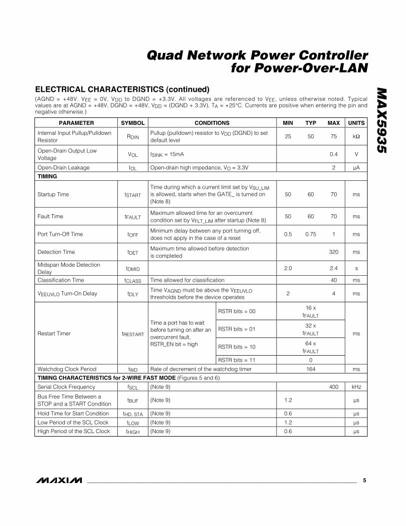
Internal Input Pullup/PulldownResistor
RDINPullup (pulldown) resistor to VDD (DGND) to setdefault level
25 50 75 kΩ
Open-Drain Output LowVoltage
VOL ISINK = 15mA 0.4 V
Open-Drain Leakage IOL Open-drain high impedance, VO = 3.3V 2 µA
TIMING
Startup Time tSTART
Time during which a current limit set by VSU_LIMis allowed, starts when the GATE_ is turned on(Note 8)
50 60 70 ms
Fault Time tFAULTMaximum allowed time for an overcurrentcondition set by VFLT_LIM after startup (Note 8)
50 60 70 ms
Port Turn-Off Time tOFFMinimum delay between any port turning off,does not apply in the case of a reset
0.5 0.75 1 ms
Detection Time tDETMaximum time allowed before detectionis completed
320 ms
Midspan Mode DetectionDelay
tDMID 2.0 2.4 s
Classification Time tCLASS Time allowed for classification 40 ms
VEEUVLO Turn-On Delay tDLYTime VAGND must be above the VEEUVLOthresholds before the device operates
2 4 ms
RSTR bits = 0016 x
tFAULT
RSTR bits = 0132 x
tFAULT
RSTR bits = 1064 x
tFAULT
Restart Timer tRESTART
Ti m e a p or t has to w ai tb efor e tur ni ng on after anover cur r ent faul t,RS TR_E N b i t = hi g h
RSTR bits = 11 0
ms
Watchdog Clock Period tWD Rate of decrement of the watchdog timer 164 ms
TIMING CHARACTERISTICS for 2-WIRE FAST MODE (Figures 5 and 6)
Serial Clock Frequency fSCL (Note 9) 400 kHz
Bus Free Time Between aSTOP and a START Condition
tBUF (Note 9) 1.2 µs
Hold Time for Start Condition tHD, STA (Note 9) 0.6 µs
Low Period of the SCL Clock tLOW (Note 9) 1.2 µs
High Period of the SCL Clock tHIGH (Note 9) 0.6 µs
MA
X5
93
5
Quad Network Power Controllerfor Power-Over-LAN
6 _______________________________________________________________________________________
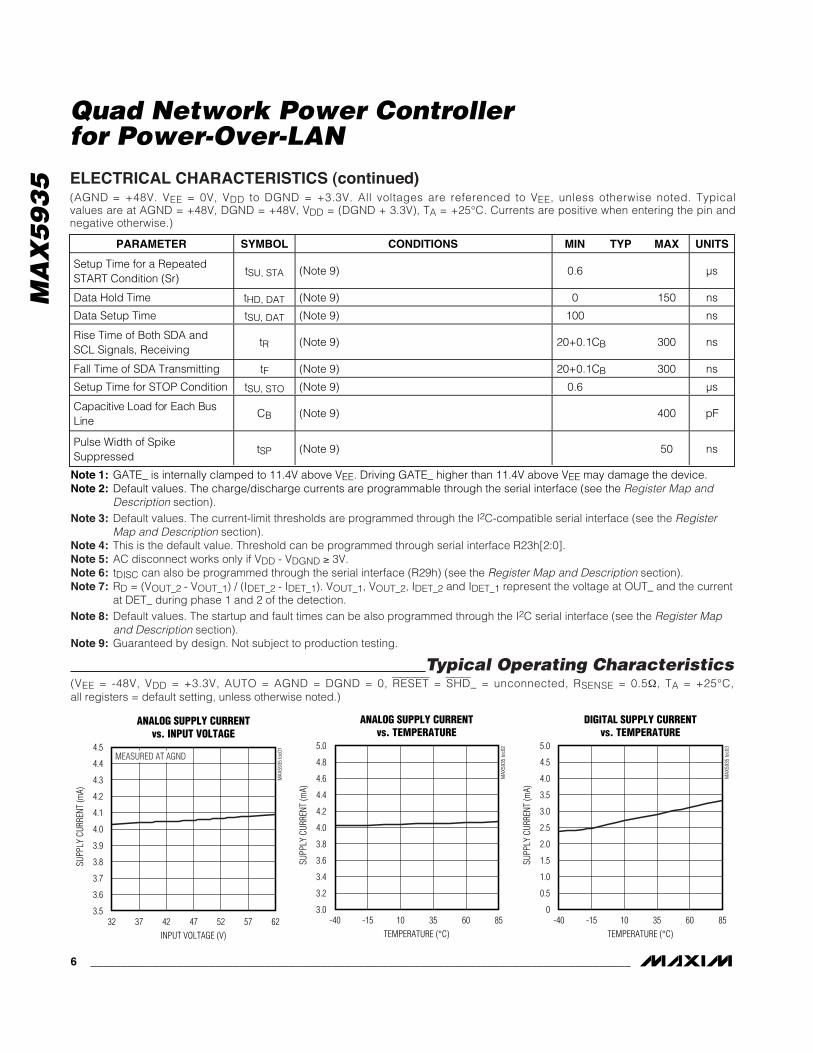
Note 1: GATE_ is internally clamped to 11.4V above VEE. Driving GATE_ higher than 11.4V above VEE may damage the device.Note 2: Default values. The charge/discharge currents are programmable through the serial interface (see the Register Map and
Description section).Note 3: Default values. The current-limit thresholds are programmed through the I2C-compatible serial interface (see the Register
Map and Description section).Note 4: This is the default value. Threshold can be programmed through serial interface R23h[2:0].Note 5: AC disconnect works only if VDD - VDGND ≥ 3V.Note 6: tDISC can also be programmed through the serial interface (R29h) (see the Register Map and Description section).Note 7: RD = (VOUT_2 - VOUT_1) / (IDET_2 - IDET_1). VOUT_1, VOUT_2, IDET_2 and IDET_1 represent the voltage at OUT_ and the current
at DET_ during phase 1 and 2 of the detection.Note 8: Default values. The startup and fault times can be also programmed through the I2C serial interface (see the Register Map
and Description section).Note 9: Guaranteed by design. Not subject to production testing.
ANALOG SUPPLY CURRENTvs. INPUT VOLTAGE
MAX
5935
toc0
1
INPUT VOLTAGE (V)
SUPP
LY C
URRE
NT (m
A)
5752474237
3.6
3.7
3.8
3.9
4.0
4.1
4.2
4.3
4.4
4.5
3.532 62
MEASURED AT AGND
ANALOG SUPPLY CURRENTvs. TEMPERATURE
MAX
5935
toc0
2
TEMPERATURE (°C)
SUPP
LY C
URRE
NT (m
A)
603510-15
3.2
3.4
3.6
3.8
4.0
4.2
4.4
4.6
4.8
5.0
3.0-40 85
DIGITAL SUPPLY CURRENTvs. TEMPERATURE
MAX
5935
toc0
3
TEMPERATURE (°C)
SUPP
LY C
URRE
NT (m
A)
603510-15
0.5
1.0
1.5
2.0
2.5
3.0
3.5
4.0
4.5
5.0
0-40 85
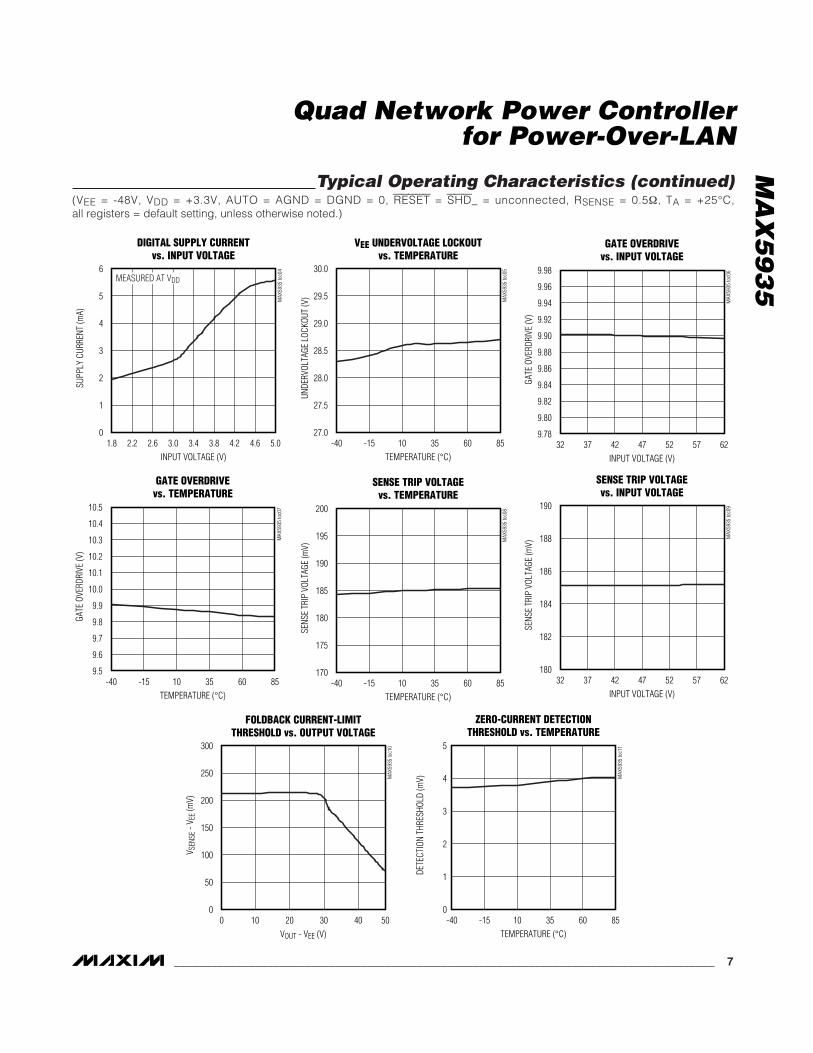
Typical Operating Characteristics(VEE = -48V, VDD = +3.3V, AUTO = AGND = DGND = 0, RESET = SHD_ = unconnected, RSENSE = 0.5Ω, TA = +25°C, all registers = default setting, unless otherwise noted.)
ELECTRICAL CHARACTERISTICS (continued)(AGND = +48V. VEE = 0V, VDD to DGND = +3.3V. All voltages are referenced to VEE, unless otherwise noted. Typical values are at AGND = +48V, DGND = +48V, VDD = (DGND + 3.3V), TA = +25°C. Currents are positive when entering the pin andnegative otherwise.)
PARAMETER SYMBOL CONDITIONS MIN TYP MAX UNITS
Setup Time for a RepeatedSTART Condition (Sr)
tSU, STA (Note 9) 0.6 µs
Data Hold Time tHD, DAT (Note 9) 0 150 ns
Data Setup Time tSU, DAT (Note 9) 100 ns
Rise Time of Both SDA andSCL Signals, Receiving
tR (Note 9) 20+0.1CB 300 ns
Fall Time of SDA Transmitting tF (Note 9) 20+0.1CB 300 ns
Setup Time for STOP Condition tSU, STO (Note 9) 0.6 µs
C ap aci ti ve Load for E ach BusLi ne
CB (Note 9) 400 pF
Pulse Width of SpikeSuppressed
tSP (Note 9) 50 ns
MA
X5
93
5
Quad Network Power Controllerfor Power-Over-LAN
_______________________________________________________________________________________ 7
DIGITAL SUPPLY CURRENTvs. INPUT VOLTAGE
MAX
5935
toc0
4
INPUT VOLTAGE (V)
SUPP
LY C
URRE
NT (m
A)
4.64.23.83.43.02.62.2
1
2
3
4
5
6
01.8 5.0
MEASURED AT VDD
VEE UNDERVOLTAGE LOCKOUTvs. TEMPERATURE
MAX
5935
toc0
5
TEMPERATURE (°C)
UNDE
RVOL
TAGE
LOC
KOUT
(V)
603510-15
27.5
28.0
28.5
29.0
29.5
30.0
27.0-40 85
GATE OVERDRIVEvs. INPUT VOLTAGE
MAX
5935
toc0
6
INPUT VOLTAGE (V)
GATE
OVE
RDRI
VE (V
)
5752474237
9.80
9.82
9.84
9.86
9.88
9.90
9.92
9.94
9.96
9.98
9.7832 62
GATE OVERDRIVEvs. TEMPERATURE
MAX
5935
toc0
7
TEMPERATURE (°C)
GATE
OVE
RDRI
VE (V
)
603510-15
9.6
9.7
9.8
9.9
10.0
10.1
10.2
10.3
10.4
10.5
9.5-40 85
SENSE TRIP VOLTAGEvs. TEMPERATURE
MAX
5935
toc0
8
TEMPERATURE (°C)
SENS
E TR
IP V
OLTA
GE (m
V)
603510-15
175
180
185
190
195
200
170-40 85
SENSE TRIP VOLTAGEvs. INPUT VOLTAGE
MAX
5935
toc0
9
INPUT VOLTAGE (V)
SENS
E TR
IP V
OLTA
GE (m
V)
5752474237
182
184
186
188
190
18032 62
FOLDBACK CURRENT-LIMITTHRESHOLD vs. OUTPUT VOLTAGE
MAX
5935
toc1
0
VOUT - VEE (V)
V SEN
SE -
V EE (
mV)
40302010
50
100
150
200
250
300
00 50
ZERO-CURRENT DETECTIONTHRESHOLD vs. TEMPERATURE
MAX
5935
toc1
1
TEMPERATURE (°C)
DETE
CTIO
N TH
RESH
OLD
(mV)
603510-15
1
2
3
4
5
0-40 85
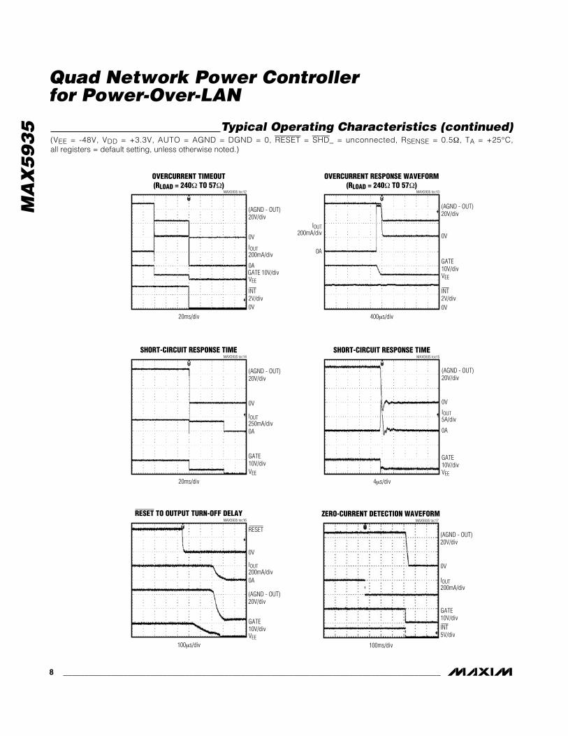
Typical Operating Characteristics (continued)(VEE = -48V, VDD = +3.3V, AUTO = AGND = DGND = 0, RESET = SHD_ = unconnected, RSENSE = 0.5Ω, TA = +25°C, all registers = default setting, unless otherwise noted.)
MA
X5
93
5
Quad Network Power Controllerfor Power-Over-LAN
8 _______________________________________________________________________________________
OVERCURRENT TIMEOUT(RLOAD = 240Ω TO 57Ω)
MAX5935 toc12
20ms/div
0V
IOUT200mA/div
VEEGATE 10V/div0A
INT2V/div
(AGND - OUT)20V/div
0V
OVERCURRENT RESPONSE WAVEFORM(RLOAD = 240Ω TO 57Ω)
MAX5935 toc13
400µs/div
0V
IOUT200mA/div
GATE10V/divVEE
0A
INT2V/div
(AGND - OUT)20V/div
0V
SHORT-CIRCUIT RESPONSE TIMEMAX5935 toc14
20ms/div
0V
IOUT250mA/div
GATE10V/divVEE
0A
(AGND - OUT)20V/div
SHORT-CIRCUIT RESPONSE TIMEMAX5935 toc15
4µs/div
0V
IOUT5A/div
GATE10V/divVEE
0A
(AGND - OUT)20V/div
RESET TO OUTPUT TURN-OFF DELAYMAX5935 toc16
100µs/div
0V
IOUT200mA/div
GATE10V/divVEE
0A
RESET
(AGND - OUT)20V/div
ZERO-CURRENT DETECTION WAVEFORMMAX5935 toc17
100ms/div
0V
IOUT200mA/div
GATE10V/divINT5V/div
(AGND - OUT)20V/div
Typical Operating Characteristics (continued)(VEE = -48V, VDD = +3.3V, AUTO = AGND = DGND = 0, RESET = SHD_ = unconnected, RSENSE = 0.5Ω, TA = +25°C, all registers = default setting, unless otherwise noted.)

MA
X5
93
5
Quad Network Power Controllerfor Power-Over-LAN
_______________________________________________________________________________________ 9
OVERCURRENT RESTART DELAYMAX5935 toc18
400ms/div
0V
0A
IOUT200mA/div
GATE10V/divVEE
(AGND - OUT)20V/div
STARTUP WITH VALID PD(25kΩ AND 0.1µF)
MAX5935 toc19
100ms/div
0V
IOUT100mA/div
GATE_
VEE
(AGND - OUT)20V/div
DETECTION WITH INVALID PD(25kΩ AND 10µF)
MAX5935 toc20
40ms/div
0V
IOUT1mA/div
(AGND - OUT)2V/div
DETECTION WITH INVALID PD (15kΩ)MAX5935 toc21
100ms/div
0V
0A
IOUT1mA/div
(AGND - OUT)5V/div
DETECTION WITH INVALID PD (33kΩ)MAX5935 toc22
100ms/div
0V
0A
IOUT1mA/div
(AGND - OUT)5V/div
STARTUP IN MIDSPAN MODEWITH VALID PD (25kΩ AND 0.1µF)
MAX5935 toc23
100ms/div
0V
0A
IOUT100mA/div
VEE
GATE_10V/div
(AGND - OUT)20V/div
Typical Operating Characteristics (continued)(VEE = -48V, VDD = +3.3V, AUTO = AGND = DGND = 0, RESET = SHD_ = unconnected, RSENSE = 0.5Ω, TA = +25°C, all registers = default setting, unless otherwise noted.)

MA
X5
93
5
Quad Network Power Controllerfor Power-Over-LAN
10 ______________________________________________________________________________________
DETECTION WITH MIDSPAN MODEWITH INVALID PD (15kΩ)
MAX5935 toc24
400ms/div
0V
0A
IOUT1mA/div
VEE
GATE_10V/div
(AGND - OUT)5V/div
DETECTION WITH MIDSPAN MODEWITH INVALID PD (33kΩ)
MAX5935 toc25
400ms/div
0V
0A
IOUT1mA/div
VEE
GATE_10V/div
(AGND - OUT)5V/div
DETECTION WITH OUTPUT SHORTEDMAX5935 toc26
40ms/div
0V
0A
IOUT1mA/div
VEE
GATE_10V/div
(AGND - OUT)5V/div
DETECTION WITH INVALID PD (OPEN CIRCUIT,USING TYPICAL OPERATING CIRCUIT 1)
MAX5935 toc27
100ms/div
0A
0V
IOUT1mA/div
VEE
GATE_10V/div
(AGND - OUT)5V/div
DETECTION WITH INVALID PD (OPEN CIRCUIT,USING TYPICAL OPERATING CIRCUIT 2)
MAX5935 toc28
100ms/div
IOUT2mA/div
0V
GATE_10V/div
(AGND-OUT)5V/div
STARTUP WITH DIFFERENT PD CLASSESMAX5935 toc29
40ms/div
IOUT10mA/div
(AGND - OUT)5V/div
CLASS0CLASS1
CLASS2CLASS3
CLASS4
Typical Operating Characteristics (continued)(VEE = -48V, VDD = +3.3V, AUTO = AGND = DGND = 0, RESET = SHD_ = unconnected, RSENSE = 0.5Ω, TA = +25°C, all registers = default setting, unless otherwise noted.)

MA
X5
93
5
Quad Network Power Controllerfor Power-Over-LAN
______________________________________________________________________________________ 11
PIN NAME FUNCTION
1 RESETHardware Reset. Pull RESET low for at least 300µs to reset the device. All internal registers reset totheir default value. The address (A0–A3), and AUTO and MIDSPAN input logic levels latch on duringlow-to-high transition of RESET. Internally pulled up to VDD with a 50kΩ resistor.
2 MIDSPANMIDSPAN Mode Input. An internal 50kΩ pulldown resistor to DGND sets the default mode to endpointPSE operation (power-over-signal pairs). Pull MIDSPAN TO VDIG to set MIDSPAN operation. TheMIDSPAN value latches after the IC is powered up or reset (see the PD Detection section).
3 INTOpen-Drain Interrupt Output. INT goes low whenever a fault condition exists. Reset the fault conditionusing software or by pulling RESET low (see the Interrupt section of the Detailed Description for moreinformation about interrupt management).
4 SCL Serial Interface Clock Line
5 SDAOUTSerial Output Data Line. Connect the data line optocoupler input to SDAOUT (see the TypicalApplication Circuit). Connect SDAOUT to SDAIN if using a 2-wire I2C-compatible system.
6 SDAINSerial Interface Input Data Line. Connect the data line optocoupler output SDAIN (see the TypicalApplication Circuit). Connect SDAIN to SDAOUT if using a 2-wire wire I2C-compatible system.
7–10 A3, A2, A1, A0Address Bit. A3, A2, A1, and A0 form the lower part of the device’s address. Address inputs defaulthigh with an internal 50kΩ pullup resistor to VDD. The address values latch when VDD or VEE rampsup and exceeds its UVLO threshold or after a reset. The 3 MSB bits of the address are set to 010.
11–14DET1, DET2,DET3, DET4
Detection and Classification Voltage Output. Use DET1 to set the detection and classification probevoltages on port 1. Use DET1 for the AC voltage sensing of port 1 when using the AC disconnectscheme (see the Typical Application Circuit).
15 DGND Connect to Digital Ground16 VDD Positive Digital Supply. Connect to digital supply (referenced to DGND).
17–20SHD1, SHD2,SHD3, SHD4
Port Shutdown Input. Pull SHD_ low to turn-off the external FET on port_. Internally pulled up to VDDwith a 50kΩ resistor.
21 AGND Analog Ground. Connect to the high-side analog supply.
22, 25,29, 32
SENSE4, SENSE3,SENSE2, SENSE1
MOSFET Source Current-Sense Negative Input. Connect to the source of the power MOSFET andconnect a current-sense resistor between SENSE_ and VEE (see the Typical Application Circuit).
23, 26,30, 33
GATE4, GATE3,GATE2, GATE1
Port_ MOSFET Gate Driver. Connect GATE_ to the gate of the external FET (see the TypicalApplication Circuit).
24, 27,31, 34
OUT4, OUT3,OUT2, OUT1
MOSFET Drain-Output Voltage Sense. Connect OUT_ to the power MOSFET drain through a resistor(100Ω to 100kΩ). The low leakage at OUT_ limits the drop across the resistor to less than 100mV(see the Typical Application Circuit).
28 VEELow-Side Analog Supply Input. Connect the low-side analog supply to VEE (-48V). Bypass with a 1µFcapacitor between AGND and VEE.
35 AUTO
AUTO or SHUTDOWN Mode Input. Force high to enter AUTO mode after a reset or power-up. Drivelow to put the MAX5935 into SHUTDOWN mode. In SHUTDOWN mode, software controls theoperational modes of the MAX5935. A 50kΩ internal pulldown resistor defaults AUTO low. AUTOlatches when VDD or VEE ramps up and exceeds its UVLO threshold or when the device resets.Software commands can take the MAX5935 out of AUTO while AUTO is high.
36 OSC_IN
Oscillator Input. AC-disconnect detection function uses OSC_IN. Connect a 100Hz ±10%, 2VP-P±5%, +1.2V offset sine wave to OSC_IN. If the oscillator positive peak falls below OSC_FAILthreshold of 2V, the ports that have the AC function enabled shut down and are not allowed to powerup. When not using the AC-disconnect detection function, leave OSC_IN unconnected.
Pin Description

MA
X5
93
5
Detailed DescriptionThe MAX5935 four-port network power controller con-trols -32V to -60V negative supply rail systems. Use theMAX5935, which is compliant with the IEEE 802.3afstandard for power-sourcing equipment (PSE) inpower-over-LAN applications. The MAX5935 providesPower Device (PD) discovery, classification, currentlimit, both DC and AC load disconnect detections, and
other necessary functions for an IEEE 802.3af-compli-ant PSE. The MAX5935 can be used in either endpointPSE (LAN Switch/Router) or midspan PSE (PowerInjector) applications.
The MAX5935 is fully software-configurable and pro-grammable with more than 25 internal registers. Thedevice features an I2C-compatible, 3-wire serial inter-face and a class-over-current detection. The class-
Quad Network Power Controllerfor Power-Over-LAN
12 ______________________________________________________________________________________
50µA
90µA100mAMAX
FASTDISCHARGECONTROL
212mV182mV
13V CLAMP
CURRENT-LIMITDETECTOR
4mV
OVERCURRENT (OVC)
OPEN CIRCUIT(OC)
CURRENTLIMIT (ILIM)
PWR_EN
10V
VOLTAGESENSING
FOLDBACKCONTROL
9-BIT ADCCONVERTER
VOLTAGE PROBINGAND
CURRENT-LIMITCONTROL
CURRENT SENSING
SENSE_
GATE_
OUT_
DET_
A = 3
ACDETECTION
ACD_ENABLE
AC DISCONNECTSIGNAL(ACD)
ACDREFERENCE
CURRENT
DETECTION/CLASSIFICATION
SM
PORTSTATE
MACHINE(SM)
REGISTER FILE
SERIALPORT
INTERFACE(SPI)
AUTO
MIDSPAN
A0
A1
A2
A3
ANALOGBIAS/
SUPPLYMONITOR
AGND
VEE
+10V ANALOG
+5V DIG
VOLTAGEREFERENCES
CURRENTREFERENCES
CENTRAL LOGIC UNIT(CLU)
DGNDOSC_INSCL SDAIN SDAOUTVDD
OSCILLATOR MONITOR
SHD_
RESET
INT
MAX5935
Figure 1. MAX5935 Functional Diagram

over-current detection function enables system powermanagement where it detects a PD that draws morecurrent than the allowable amount for its class. TheMAX5935’s extensive programmability enhances sys-tem flexibility and allows for uses in other applications.
The MAX5935 has four different operating modes: automode, semi-auto mode, manual mode, and shutdownmode (see the Operation Modes section). A specialWatchdog feature allows the hardware to gracefullytake over control if the software/firmware crashes. Acadence timing feature allows the MAX5935 to be usedin midspan systems.
The MAX5935 provides input undervoltage lockout,input undervoltage detection, input overvoltage lockout,overtemperature protection, output voltage slew-ratelimit during startup, power-good status, and fault sta-tus. The MAX5935’s programmability includes gate-charging current, current-limit threshold, startuptimeout, overcurrent timeout, autorestart duty cycle,PD-disconnect AC-detection threshold, and PD-discon-nect detection timeout.
The MAX5935 communicates with the system micro-controller through an I2C-compatible interface. TheMAX5935 features separate input and output data lines(SDAIN and SDAOUT) for use with optocoupler isola-tion. The MAX5935 is a slave device. Its four addressinputs allow 16 unique MAX5935 addresses. A sepa-rate INT output and four independent shutdown inputs(SHD_) allow fast interrupt signals between theMAX5935 and the microcontroller. A RESET inputallows hardware reset of the device.
ResetReset is a condition the MAX5935 enters following anyof the following conditions:
• After power-up (VEE and VDD rise above their UVLOthresholds)
• Hardware reset. The RESET input is driven low andup high again any time after power-up.
• Software reset. Writing a 1 into R1Ah[4] any timeafter power-up.
• Thermal shutdown
During a reset, the MAX5935 resets its register map tothe Reset state as shown in Table 30 and latches in thestate of AUTO (pin 35) and MIDSPAN (pin 2). Duringnormal operation, changes at the AUTO and MIDSPANinputs are ignored. While the condition that caused thereset persists (i.e., high temperature, RESET input lowor UVLO conditions), the MAX5935 will not acknowl-edge any addressing from the serial interface.
Port Reset (R1Ah[3:0])Set high anytime during normal operation to turn offpower and clear the events and status registers of thecorresponding port. Port reset only resets the eventsand status registers.
Operation ModesThe MAX5935 contains four independent but identicalstate machines to provide reliable and real-time controlof the four network ports. Each state machine has fourdifferent operating modes: auto, semi-auto, manual,and shutdown. Auto mode allows the device to operateautomatically without any software supervision. Semi-auto mode, upon request, continuously detects andclassifies a device connected to a port but does notpower up that port until instructed by software. Manualmode allows total software control of the device and isuseful in system diagnostic. Shutdown mode terminatesall activities and securely turns off power to the ports.Switching between AUTO, SEMI, or MANUAL modedoes not take effect until the part finishes its currenttask. When the port is set into SHUTDOWN mode, allthe port operations are immediately stopped and theport remains idle until SHUTDOWN is exited.
Automatic (AUTO) ModeEnter automatic (AUTO) mode by forcing the AUTOinput high prior to a reset, or by setting R12h[P_M1,P_M0] to [1,1] during normal operation (see Tables15 and 15a). In AUTO mode, the MAX5935 performsdetection and classification, and powers up the portautomatically once a valid power device (PD) is detect-ed at the port. If a valid PD is not connected at the port,the MAX5935 repeats the detection routine continuous-ly until a valid PD is connected.
Going into AUTO mode, the DET_EN and CLASS_ENbits are set to high and stay high unless changed bysoftware. Using software to set DET_EN and/orCLASS_EN low causes the MAX5935 to skip detectionand/or classification. As a protection, disabling theDetection routine in AUTO mode will not allow the cor-responding port to power up, unless the DET_BYP(R23H[4]) is set to 1.
The AUTO status is latched into the register only duringa reset. Any changes to the AUTO input after reset isignored.
Semi-Automatic (SEMI) ModeEnter semi-automatic (SEMI) mode by sett ingR12h[P_M1,P_M0] to [1,0] during normal operation(see Tables 15 and 15a). In SEMI mode, the MAX5935,upon request, performs detection and/or classificationrepeatedly but does not power up the port(s), regard-less of the status of the port connection.
MA
X5
93
5
Quad Network Power Controllerfor Power-Over-LAN
______________________________________________________________________________________ 13

MA
X5
93
5 Setting R19h[PWR_ON_] (Table 21) high immediatelyterminates detection/classification routines and turns onpower to the port(s).
R14h[DET_EN_, CLASS_EN_] default to low in SEMImode. Use software to set R14h[DET_EN_,CLASS_EN_] to high to start the detection and/or classi-fication routines. R14h[DET_EN_, CLASS_EN_] arereset every time the software commands a power-off ofthe port (either through reset or PWR_OFF). In any othercases, the status of the bits is left unchanged (includingwhen the state machine turns off the power because aload disconnect or a fault condition is encountered).
MANUAL ModeEnter MANUAL mode by setting R12h[P_M1,P_M0] to[0,1] during normal operation (see Tables 15 and 15a).MANUAL mode allows the software to dictate anysequence of operation. Write a 1 to both R14h[DET_EN_] and R14h[CLASS_EN_] start detection and classi-fication operations, respectively and in that priorityorder. After execution, the command is cleared fromthe register(s). PWR_ON_ has highest priority. SettingPWR_ON_ high at any time causes the device to enterthe powered mode immediately. Setting DET_EN andCLASS_EN high at the same time causes detection tobe performed first. Once in the powered state, thedevice ignores DET_EN_ or CLASS_EN_ commands.
When switching to MANUAL mode from another mode,DET_EN_, CLASS_EN_ default to low. These bitsbecome “pushbutton” rather than configuration bits(i.e., writing ones to these bits while in MANUAL modecommands the device to execute one cycle of detec-tion and/or classification. The bits are reset back tozeros at the end of the execution). Putting the MAX5935into shutdown mode immediately turns off power andhalts all operations to the corresponding port. Theevent and status bits of the affected port(s) are alsocleared. In SHUTDOWN mode, the DET_EN,CLASS_EN, and PWR_ON commands are ignored.
In SHUTDOWN mode, the serial interface operates normally.
WatchdogR1Dh, R1Eh, and R1Fh registers control Watchdog oper-ation. The Watchdog function, when enabled, allows theMAX5935 to gracefully take over control or securely shutdown the power to the ports in case of software/firmwarecrashes. Contact the factory for more details.
PD DetectionWhen PD detection is activated, the MAX5935 probesthe output for a valid PD. After each detection cycle,the device sets the DET_END_ bit R04h/05h[3:0] highand reports the detection results in the status registersR0Ch[2:0], R0Dh[2:0], R0Eh[2:0], and R0Fh[2:0]. TheDET_END_ bit is reset to low when read through R05hor after a port reset. Both DET_END_bit status registersare cleared after the port powers down.
A valid PD has a 25kΩ discovery signature characteris-tic as specified in the IEEE 802.3af standard. Table 1shows the IEEE 802.3af specification for a PSE detect-ing a valid PD signature (see the Typical ApplicationCircuit and Figure 2). The MAX5935 can probe and cat-egorize different types of devices connected to the portsuch as a valid PD, an open circuit, a low resistive load,a high resistive load, a high capacitive load, a positiveDC supply, or a negative DC supply.
During detection, the MAX5935 turns off the externalMOSFET and forces two probe voltages through theDET_ input. The current through the DET_ input is mea-sured as well as the voltage at OUT_. A two-point slopemeasurement is used as specified by the IEEE 802.3afstandard to verify the device connected to the port. TheMAX5935 implements appropriate settling times and a100ms digital integration to reject 50Hz/60Hz power-line noise coupling.
An external diode, in series with the DET_ input,restricts PD detection to the 1st quadrant as specifiedby the IEEE 802.3af standard. To prevent damage tonon-PD devices and to protect itself from an outputshort circuit, the MAX5935 limits the current into DET_to less than 2mA maximum during PD detection.
In midspan mode, the MAX5935 waits 2.2s beforeattempting another detection cycle after every faileddetection. The first detection, however, happens imme-diately after issuing the detection command.
Power Device Classification(PD Classification)
During the PD classification mode, the MAX5935 forcesa probe voltage (-18V) at DET_ and measures the cur-rent into DET_. The measured current determines theclass of the PD.
After each classification cycle, the device sets theCL_END_ bit (R04h/05h[7:4]) high and reports the clas-sification results in the status registers R0Ch[6:4],R0Dh[6:4], R0Eh[6:4], and R0Fh[6:4]. The CL_END_ bitis reset to low when read through register R05h or aftera port reset. Both Class_END_bit status registers arecleared after the port powers down.
Quad Network Power Controllerfor Power-Over-LAN
14 ______________________________________________________________________________________

Table 2 shows the IEEE 802.3af requirement for a PSEclassifying a PD at the Power Interface (PI).
Powered StateWhen the part enters PWR MODE, the tSTART and tDISCtimers are reset. Before turning on the power, the part
checks if any other port is not turning on and if thetFAULT timer is zero. Another check is performed if theACD_EN bit is set; in this case, the OSC_FAIL bit mustbe low (oscillator is okay) for the port to be powered.
If these conditions are met, then the part enters startupwhere it turns on power to the port. An internal signal,POK_, is asserted high when VOUT is within 2V fromVEE. PGOOD_ status bits are set high if POK_ stayshigh longer than tPGOOD. PGOOD immediately resetswhen POK goes low.
The PWR_CHG bit sets when a port powers up or down.PWR_EN sets when a port powers up and resets when aport shuts down. The port shutdown timer lasts 0.5msand prevents other ports from turning off during that peri-od, except in the case of emergency shutdowns (RESET= L, RESET_IC = H, VEEUVLO, VDDUVLO, and TSHD).
The MAX5935 always checks the status of all ports beforeturning off. A priority logic system determines the order toprevent the simultaneous turn-on or turn-off of the ports.The port with the lesser ordinal number gets priority overthe others (i.e., Port 1 turns on first, Port 2 second, Port 3third and Port 4 fourth). Setting PWR_OFF_ high turns offpower to the corresponding port.
MA
X5
93
5
Quad Network Power Controllerfor Power-Over-LAN
______________________________________________________________________________________ 15
PARAMETER SYMBOL MIN MAX UNITS ADDITIONAL INFORMATION
Open-Circuit Voltage VOC — 30 V In detection mode only.
Short-Circuit Current ISC — 5 mA In detection mode only.
Valid Test Voltage VVALID 2.8 10 V
Voltage Difference BetweenTest Points
∆VTEST 1 — V
Time Between Any Two TestPoints
tBP 2 — ms This timing implies a 500Hz maximum probing frequency.
Slew Rate VSLEW — 0.1 V/µs
Accept Signature Resistance RGOOD 19 26.5 kΩReject Signature Resistance RBAD < 15 > 33 kΩOpen-Circuit Resistance ROPEN 500 — kΩ
Accept SignatureCapacitance
CGOOD — 150 nF
Reject SignatureCapacitance
CBAD 10 — µF
Signature Offset VoltageTolerance
VOS 0 2.0 V
Signature Offset CurrentTolerance
IOS 0 12 µA
Table 1. PSE PI Detection Modes Electrical Requirement (Table 33-2 of the IEEE 802.3af Standard)
MEASURED ICLASS (mA) CLASSIFICATION
0 to 5 Class 0
> 5 and < 8 May be Class 0 and 1
8 to 13 Class 1
> 13 and < 16 May be Class 0, 1, or 2
16 to 21 Class 2
> 21 and < 25 May be Class 0, 2, or 3
25 to 31 Class 3
> 31 and <35 May be Class 0, 3, or 4
35 to 45 Class 4
> 45 and < 51 May be Class 0 or 4
Table 2. PSE Classification of a PD (Table 33.4 of the IEEE 802.3af Standard)

MA
X5
93
5 Overcurrent ProtectionA sense resistor (RS), connected between SENSE_ andVEE, monitors the load current. Under all circum-stances, the voltage across RS never exceeds thethreshold VSU_LIM. If SENSE_ exceeds VSU_LIM, aninternal current-limiting circuit regulates the GATE volt-age, limiting the current to ILIM = VSU_LIM / RS. Duringtransient conditions, if the SENSE_ voltage exceedsVSU_LIM, a fast pulldown circuit activates in order toquickly recover from the current overshoot. Duringstartup, if the current-limit condition persists, when thestartup timer, tSTART, times out, the port shuts off andthe STRT_FLT_ bit is set. In the normal powered state,the MAX5935 checks for overcurrent conditions asdetermined by VFLT_LIM = ~88% of VSU_LIM. ThetFAULT counter sets the maximum-allowed continuous overcurrent period. The tFAULT counter increases whenVSENSE exceeds VFLT_LIM and decreases at a slowerpace when VSENSE drops below VFLT_LIM. A slowerdecrement for the tFAULT counter allows for detectingrepeated short-duration overcurrents. When the counterreaches the tFAULT limit, the MAX5935 powers off theport and asserts the IMAX_FLT_ bit. For a continuousoverstress, a fault latches exactly after a period oftFAULT. VSU_LIM, is programmable using R27h[4-7].tFAULT is programmable using R16h[2-3] and R28[4-7].
After power-off due to an overcurrent fault, and if theRSTR_EN bit is set, the tFAULT timer is not immediatelyreset but starts decrementing at the same slower pace.The MAX5935 allows the port to be powered on onlywhen the tFAULT counter is at zero. This feature sets anautomatic duty-cycle protection to the external MOSFETto avoid overheating. The duty cycle is programmableusing R16h[6-7].
The MAX5935 continuously flags when the currentexceeds the maximum current allowed for the class asindicated in the CLASS status register. When classovercurrent occurs, the MAX5935 sets the IVC bit inregister R09h.
Foldback CurrentDuring startup and normal operation, an internal circuitsenses the voltage at OUT_ and reduces the current-limit value when (VOUT_ - VEE) > 30V. The foldbackfunction helps to reduce the power dissipation on theFET. The current limit eventually reduces to 1/3 of ILIMwhen (VOUT_ - VEE ) > 50V (see Figure 4).
Quad Network Power Controllerfor Power-Over-LAN
16 ______________________________________________________________________________________
Figure 2. Detection, Classification, and Power-Up PortSequence
OUT_
-4V
-9V
-18V
-48V
ttDETI tDETII tCLASS
150ms 150ms 21.3ms
0V
0V80ms
Figure 3. PGOOD Timing
PGOOD
POKtPGOOD

MOSFET Gate DriverConnect the gate of the external n-channel MOSFET toGATE_. An internal 50µA current source pulls GATE_ to(VEE + 10V) to turn on the MOSFET. An internal 40µAcurrent source pulls down GATE_ to VEE to turn off theMOSFET.
The pullup and pulldown current controls the maximumslew rate at the output during turn-on or turn-off. Thepullup current (gate-charging current) is programmableusing R23h[5-7]. Use the following equation to set themaximum slew rate:
where CGD is the total capacitance between GATE andDRAIN of the external FET. Current limit and the capac-itive load at the drain control the slew rate during start-up. During current-limit regulation, the MAX5935manipulates the GATE_ voltage to control the voltage atSENSE_. A fast pulldown activates if SENSE_ over-shoots the limit threshold. The fast pulldown currentincreases with the amount of overshoot. The maximumfast pulldown current is 100mA.
During turn-off when the GATE voltage reaches a valuelower than 1.2V, a strong pulldown switch is activatedto keep the FET securely off.
Digital LogicVDD supplies power for the internal logic circuitry. VDDranges from +1.71V to +3.7V and determines the logicthresholds for the CMOS connections (SDAIN,SDAOUT, SCL, AUTO, SHD_, A_). This voltage rangeenables the MAX5935 to interface with a nonisolatedlow-voltage microcontroller. The MAX5935 checks the
digital supply for compatibility with the internal logic.The MAX5935 also features a VDD undervoltage lockout(VDDUVLO) of +1.35V. A VDDUVLO condition keeps theMAX5935 in reset and the ports shut off. Bit 0 in thesupply event register shows the status of VDDUVLO(Table 11) after VDD has recovered. All logic inputs andoutputs reference to DGND. DGND and AGND arecompletely isolated internally to the MAX5935. In acompletely isolated system, the digital signal can bereferenced indifferently to VAGND or VEE or at voltageseven higher than AGND (up to 60V). VDD - VDGND mustbe greater than 3.0V when VDGND ≤ (VEE + 3.0V)
When using the AC disconnect-detection feature,AGND must be connected directly to DGND and VDDmust be greater than +3V. In this configuration, con-nect DGND to AGND at a single point in the system asclose to MAX5935 as possible.
Hardware ShutdownSHD_ shuts down the respective ports without usingthe serial interface. Hardware shutdown offers an emer-gency turn-off feature that allows a fast disconnect ofthe power supply from the port. Pull SHD_ low toremove power.
InterruptThe MAX5935 contains an open-drain logic output (INT)that goes low when an interrupt condition exists. R00hand R01h (Tables 5 and 6) contain the definitions of theinterrupt registers. The mask register R01h determinesevents that trigger an interrupt. As a response to aninterrupt, the controller reads the status of the event reg-ister to determine the cause of the interrupt and takessubsequent actions. Each interrupt event register alsocontains a clear-on-read (CoR) register. Readingthrough the CoR register address clears the interrupt.INT remains low when reading the interrupt through theread-only addresses. For example, to clear a startupfault on port 4 read address 09h (see Table 10). Use theglobal pushbutton bit on register 1Ah (bit 7, Table 22) toclear interrupts, or use a software or hardware reset.
Undervoltage and Overvoltage ProtectionThe MAX5935 contains several undervoltage and over-voltage protection features. Table 11 in the Register Mapand Description section shows a detailed list of theundervoltage and overvoltage protection features. Aninternal VEE undervoltage-lockout (VEEUVLO) circuitkeeps the MOSFET off and the MAX5935 in reset untilVAGND - VEE exceeds 29V for more than 3ms. An internalVEE overvoltage (VEE_OV) circuit shuts down the portswhen (VAGND - VEE) exceeds 60V. The digital supply alsocontains an undervoltage lockout (VDDUVLO).
∆
∆
Vt
IC
OUT GATE
GD=
MA
X5
93
5
Quad Network Power Controllerfor Power-Over-LAN
______________________________________________________________________________________ 17
Figure 4. Foldback Current Characteristics
50V30V
VSU_LIM
VSU_LIM / 3
(VSENSE_ - VEE)
(VOUT_ - VEE)

MA
X5
93
5 The MAX5935 also features three other undervoltageand overvoltage interrupts: VEE undervoltage interrupt(VEEUV), VDD undervoltage interrupt (VDDUV), and VDDovervoltage interrupt (VDDOV). A fault latches into thesupply events register (Table 11), but the MAX5935does not shut down the ports with a VEEUV, VDDUV, orVDDOV.
DC Disconnect MonitoringSetting R13h[DCD_EN_] bits high enables DC loadmonitoring during normal powered state. If SENSE_falls below the DC load disconnect threshold, VDCTH,for more than tDISC, the device turns off power andasserts the LD_DISC_ bit of the corresponding port.tDISC is programmable using R16h[0-1] and R27h[0-3].
AC Disconnect MonitoringThe MAX5935 features AC load disconnect monitoring.Connect an external sine wave to OSC_IN. The oscilla-tor requirements are:
• Frequency x VP-P = 200VP-P x Hz ±15%
• Positive peak voltage > +2V
• Frequency > 60Hz
• A 100Hz ±10%, 2VP-P ±5%, with +1.2V offset(VPEAK = +2.2V, typ) is recommended.
The MAX5935 buffers and amplifies 3x the externaloscillator signal and sends the signal to DET_, wherethe sine wave is AC-coupled to the output. TheMAX5935 senses the presence of the load by monitor-ing the amplitude of the AC current returned to DET_(see the Functional Diagram).
Setting R13h[ACD_EN_] bits high enable AC load dis-connect monitoring during the normal powered state. Ifthe AC current peak at the DET_ pin falls below IACTHfor more than tDISC, the device turns off power andasserts the LD_DISC_ bit of the corresponding port.IACTH is programmable using R23h[0-3].
An internal comparator checks for a proper amplitudeof the oscillator input. If the positive peak of the inputsinusoid falls below a safety value of 2V, OSC_FAILsets and the port shuts down. Power cannot be appliedto the ports when ACD_EN is set high and OSC_FAIL isset high. Leave OSC_IN unconnected or connect it toDGND when not using AC disconnect detection.
When using the AC disconnect detection feature, con-nect AGND directly to DNGD as close as possible tothe IC. The MAX5935 also requires a VDD of greaterthan +3V for this function. See the Typical ApplicationCircuit with AC disconnect for other external compo-nent requirements.
Thermal ShutdownIf the MAX5935 die temperature reaches +150°C, anovertemperature fault generates and the MAX5935shuts down and the MOSFETs turn off. The die temper-ature of the MAX5935 must cool down below +130°C toremove the overtemperature fault condition. After athermal shutdown, the part is reset.
Address InputsA3, A2, A1, and A0 represent the four LSBs of the chipaddress, the complete seven bits chip address (seeTable 3).
The four LSBs latch on the low-to-high transition ofRESET or after a power-supply start (either on VDD orVEE). Address inputs default high through an internal50kΩ pullup resistor to VDD. The MAX5935 alsoresponds to the call through a global address 60h (seethe Global Addressing and Alert Response Protocolsection).
I2C-Compatible Serial InterfaceThe MAX5935 operates as a slave that sends andreceives data through an I2C-compatible, 2-wire or 3-wire interface. The interface uses a serial data input line(SDAIN), a serial data output line (SDAOUT) and a seri-al clock line (SCL) to achieve bidirectional communica-tion between master(s) and slave(s). A master (typicallya microcontroller) initiates all data transfers to and fromthe MAX5935, and generates the SCL clock that syn-chronizes the data transfer. In most applications, con-nect the SDAIN and the SDAOUT lines together to formthe serial data line (SDA).
Using the separate input and output data lines allowsoptocoupling with the controller bus when an isolatedsupply powers the microcontroller.
The MAX5935 SDAIN line operates as input. TheMAX5935 SDAOUT operates as an open-drain output.A pullup resistor, typically 4.7kΩ, is required onSDAOUT. The MAX5935 SCL line operates only as aninput. A pullup resistor, typically 4.7kΩ, is required onSCL if there are multiple masters, or if the master in asingle-master system has an open-drain SCL output.
Serial AddressingEach transmission consists of a START condition (Figure7) sent by a master, followed by the MAX5935 7-bit slaveaddress plus R/W bit, a register address byte, one ormore data bytes, and finally a STOP condition.
Quad Network Power Controllerfor Power-Over-LAN
18 ______________________________________________________________________________________
0 1 0 A3 A2 A1 A0 R/W
Table 3. MAX5935 Address
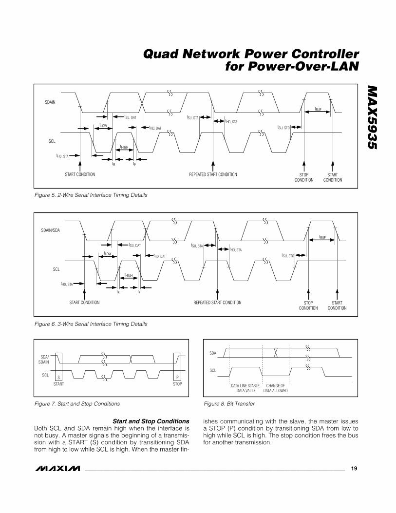
Start and Stop ConditionsBoth SCL and SDA remain high when the interface isnot busy. A master signals the beginning of a transmis-sion with a START (S) condition by transitioning SDAfrom high to low while SCL is high. When the master fin-
ishes communicating with the slave, the master issuesa STOP (P) condition by transitioning SDA from low tohigh while SCL is high. The stop condition frees the busfor another transmission.
MA
X5
93
5
Quad Network Power Controllerfor Power-Over-LAN
______________________________________________________________________________________ 19
Figure 5. 2-Wire Serial Interface Timing Details
SCL
SDAIN
tLOW
tHIGH
tR tF
tBUF
STARTCONDITION
STOPCONDITION
REPEATED START CONDITIONSTART CONDITION
tHD, STA
tSU, DAT
tHD, DAT
tSU, STAtHD, STA
tSU, STO
Figure 6. 3-Wire Serial Interface Timing Details
SCL
SDAIN/SDA
tLOW
tHIGH
tR tF
tBUF
STARTCONDITION
STOPCONDITION
REPEATED START CONDITIONSTART CONDITION
tHD, STA
tSU, DAT
tHD, DAT
tSU, STAtHD, STA
tSU, STO
Figure 8. Bit Transfer
SDA
SCL
DATA LINE STABLE;DATA VALID
.CHANGE OF
DATA ALLOWED
Figure 7. Start and Stop Conditions
START STOPS P
SDA/SDAIN
SCL

MA
X5
93
5
Bit TransferEach clock pulse transfers one data bit (Figure 8). Thedata on SDA must remain stable while SCL is high.
AcknowledgeThe acknowledge bit is a clocked 9th bit (Figure 9),which the recipient uses as a handshake receipt of eachbyte of data. Thus, each byte effectively transferredrequires 9 bits. The master generates the 9th clockpulse, and the recipient pulls down SDA (or the SDAOUTin the 3-wire interface) during the acknowledge clockpulse, such that the SDA line is stable low during thehigh period of the clock pulse. When the master trans-mits to the MAX5935, the MAX5935 generates theacknowledge bit. When the MAX5935 transmits to themaster, the master generates the acknowledge bit.
Slave AddressThe MAX5935 has a 7-bit long slave address (Figure10). The bit following the 7-bit slave address (bit eight)is the R/W bit, which is low for a write command andhigh for a read command.
010 always represent the first three bits (MSBs) of theMAX5935 slave address. Slave address bits A3, A2,A1, and A0 represent the states of the MAX5935’s A3,A2, A1, and A0 inputs, allowing up to sixteen MAX5935devices to share the bus. The states of the A3, A2, A1,
and A0 latch in upon the reset of the MAX5935 into reg-ister R11h. The MAX5935 monitors the bus continuous-ly, waiting for a START condition followed by theMAX5935’s slave address. When the MAX5935 recog-nizes its slave address, it acknowledges and is thenready for continued communication.
Global Addressing and Alert Response ProtocolThe global address call is used in writing mode to writethe same register to multiple devices (address 0x60). Inread mode (address 0x61), the global address call isused as the Alert Response address. When respondingto a global call, the MAX5935 puts out on the data line itsown address whenever its interrupt is active and so doesevery other device connected to the SDAOUT line thathas an active interrupt. After every bit is transmitted, theMAX5935 checks that the data line effectively corre-sponds to the data it is delivering. If it is not, it then backsoff and frees the data line. This litigation protocol alwaysallows the part with the lowest address to complete thetransmission. The microcontroller can then respond tothe interrupt and take proper actions. The MAX5935does not reset its own interrupt at the end of the AlertResponse protocol. The microcontroller has to do it byclearing the event register through their CoR addressesor activating the CLR_INT pushbutton.
Quad Network Power Controllerfor Power-Over-LAN
20 ______________________________________________________________________________________
Figure 9. Acknowledge
SCL
SDABY TRANSMITTER
CLOCK PULSE FOR ACKNOWLEDGEMENTSTART CONDITION
SDABY RECEIVER
1 2 8 9
S
Figure 10. Slave Address
SDA
SCL
10 A3 A2 A1 A00
MSBLSB
ACKR/W

Message Format for Writing the MAX5935A write to the MAX5935 comprises of the MAX5935’sslave address transmission with the R/W bit set to 0, fol-lowed by at least one byte of information. The first byteof information is the command byte (Figure 11). Thecommand byte determines which register of theMAX5935 is written to by the next byte, if received. Ifthe MAX5935 detects a STOP condition after receivingthe command byte, then the MAX5935 takes no furtheraction beyond storing the command byte. Any bytesreceived after the command byte are data bytes. Thefirst data byte goes into the internal register of the
MAX5935 selected by the command byte. If theMAX5935 transmits multiple data bytes before theMAX5935 detects a STOP condition, these bytes storein subsequent MAX5935 internal registers because thecontrol byte address auto-increments.
Any bytes received after the control byte are databytes. The first data byte goes into the internal registerof the MAX5935 selected by the control byte (Figure 8).
If multiple data bytes are transmitted before a STOPcondition is detected, these bytes are stored in subse-quent MAX5935 internal registers because the controlbyte address auto-increments.
MA
X5
93
5
Quad Network Power Controllerfor Power-Over-LAN
______________________________________________________________________________________ 21
Figure 11. Control Byte Received
S A A P0SLAVE ADDRESS CONTROL BYTE
ACKNOWLEDGE FROM MAX5935
ACKNOWLEDGE FROM MAX5935
D15 D14 D13 D12 D11 D10 D9 D8CONTROL BYTE IS STORED ON RECEIPT OF STOP CONDITION
R/W
Figure 12. Control and Single Data Byte Received
S A A A P0SLAVE ADDRESS CONTROL BYTE DATA BYTE
ACKNOWLEDGE FROM MAX5935
1 BYTE
AUTO-INCREMENTMEMORY WORD ADDRESS
D15 D14 D13 D12 D11 D10 D9 D8 D1 D0D3 D2D5 D4D7 D6HOW CONTROL BYTE AND DATA BYTE MAP
INTO THE REGISTER
ACKNOWLEDGE FROM MAX5935 ACKNOWLEDGE FROM MAX5935
R/W
Figure 13. ‘n’ Data Bytes Received
S A A A P0SLAVE ADDRESS CONTROL BYTE DATA BYTE
ACKNOWLEDGE FROM MAX5935
n BYTES
AUTO-INCREMENTMEMORY WORD ADDRESS
D15 D14 D13 D12 D11 D10 D9 D8 D1 D0D3 D2D5 D4D7 D6HOW CONTROL BYTE AND DATA BYTE MAP
INTO THE REGISTER
ACKNOWLEDGE FROM MAX5935 ACKNOWLEDGE FROM MAX5935
R/W

MA
X5
93
5
Message Format for ReadingThe MAX5935 reads using the MAX5935’s internallystored command byte as an address pointer, the sameway the stored command byte is used as an addresspointer for a write. The pointer auto-increments afterreading each data byte using the same rules as for awrite. Thus, a read is initiated by first configuring theMAX5935’s command byte by performing a write(Figure 12). The master now reads “n” consecutivebytes from the MAX5935, with the first data byte readfrom the register addressed by the initialized commandbyte (Figure 13). When performing read-after-write veri-fication, remember to reset the command byte’saddress because the stored control byte address auto-increments after the write.
Operation with Multiple MastersWhen the MAX5935 operates on a 2-wire interface withmultiple masters, a master reading the MAX5935should use repeated starts between the write that setsthe MAX5935’s address pointer, and the read(s) thattakes the data from the location(s). It is possible formaster 2 to take over the bus after master 1 has set upthe MAX5935’s address pointer but before master 1has read the data. If master 2 subsequently resets theMAX5935’s address pointer, then master 1’s read maybe from an unexpected location.
Command Address Auto-IncrementingAddress auto-incrementing allows the MAX5935 to beconfigured with fewer transmissions by minimizing thenumber of times the command address needs to besent. The command address stored in the MAX5935generally increments after each data byte is written orread (Table 4). The MAX5935 is designed to preventoverwrites on unavailable register addresses and unin-tentional wraparound of addresses.
Register Map And DescriptionThe interrupt register (Table 5) summarizes the eventregister status and is used to send an interrupt signal(INT goes low) to the controller. Writing a 1 to R1Ah[7]clears all interrupt and events registers. A Reset setsR00h to 00h.
INT_EN (R17h[7]) is a global interrupt mask (Table 6).The MASK_ bits activate the corresponding interruptbits in register R00h. Writing a 0 to INT_EN (R17h[7])disables the INT output.
A Reset sets R01h to AAA00A00b, where A is the stateof the AUTO input prior to the reset.
The power event register (Table 7) records changes inthe power status of the four ports. Any change inPGOOD_ (R10h[7:4]) sets PG_CHG_ to 1. Any changein the PWR_EN_ (R10h[3:0]) sets PWEN_CHG_ to 1.PG_CHG_ and PWEN_CHG_ trigger on the edges ofPGOOD_ and PWR_EN_ and do not depend on theactual level of the bits. The power event register hastwo addresses. When read through the R02h address,the content of the register is left unchanged. When readthrough the CoR R03h address, the register content willbe cleared. A Reset sets R02h/R03h = 00h.
DET_END_/CL_END_ is set high whenever detection/classification is completed on the corresponding port.A 1 in any of the CL_END_ bits forces R00h[4] to 1. A 1in any of the DET_END_ bits forces R00h[3] to 1. Aswith any of the other events register, the detect eventregister (Table 8) has two addresses. When readthrough the R04h address, the content of the register isleft unchanged. When read through the CoR R05haddress, the register content will be cleared. A Resetsets R04h/R05h = 00h.
LD_DISC_ is set high whenever the corresponding portshuts down due to detection of load removal.IMAX_FLT_ is set high when the port shuts down due toan extended overcurrent event after a successful start-up. A 1 in any of the LD_DISC_ bits forces R00h[2] to 1.A 1 in any of the IMAX_FLT_ bits forces R00h[5] to 1.As with any of the other events registers, the fault eventregister (Table 9) has two addresses. When readthrough the R06h address, the content of the register isleft unchanged. When read through the CoR R07haddress, the register content will be cleared. A resetsets R06h/R07h = 00h.
If the port remains in current limit or the PGOOD condi-tion is not met at the end of the startup period, the portshuts down and the corresponding STRT_FLT_ is set to1. A 1 in any of the STRT_FLT_ bits forces R00h[6] to 1.IVC_ is set to 1 whenever the port current exceeds themaximum allowed limit for the class (determined duringthe classification process). A 1 in any of IVC_ forcesR00h[6] to 1. When the CL_DISC (R17h[2]) is set to 1,the port will also limit the load current according to itsclass as specified in the Electrical Characteristics table.As with any of the other events registers, the startupevent register (Table 10) has two addresses. When
Quad Network Power Controllerfor Power-Over-LAN
22 ______________________________________________________________________________________
COMMAND BYTEADDRESS RANGE AUTO-INCREMENT BEHAVIOR
0x00 to 0x26Command address will auto-increment after byte read or written
0x26Command address remains at 0x26after byte written or read
Table 4. Auto-Increment Rules

MA
X5
93
5
Quad Network Power Controllerfor Power-Over-LAN
______________________________________________________________________________________ 23
ADDRESS = 00h
SYMBOL BIT R/WDESCRIPTION
SUP_FLT 7 RInterrupt signal for supply faults. SUP_FLT is the logic OR of all the bits [7:0] in register R0Ah/R0Bh(Table 8).
TSTR_FLT 6 RInterrupt signal for startup failures. TSRT_FLT is the logic OR of bits [7:0] in register R08h/R09h(Table 7).
IMAX_FLT 5 RInterrupt signal for current-limit violations. IMAX_FLT is the logic OR of bits [3:0] in registerR06h/R07h (Table 6).
CL_END 4 RInterrupt signal for completion of classification. CL_END is the logic OR of bits [7:4] in registerR04h/R05h (Table 5).
DET_END 3 RInterrupt signal for completion of detection. DET_END is the logic OR of bits [3:0] in registerR04h/R05h (Table 5).
LD_DISC 2 RInterrupt signal for load disconnection. LD_DISC is the logic OR of bits [7:4] in register R06h/R07h(Table 6).
PG_INT 1 RInterrupt signal for PGOOD status change. PG_INT is the logic OR of bits [7:4] in register R02h/R03h(Table 4).
PE_INT 0 RInterrupt signal for power-enable status change. PEN_INT is the logic OR of bits [3:0] in registerR02h/R03h (Table 4).
Table 5. Interrupt Register
ADDRESS = 01h
SYMBOL BIT R/WDESCRIPTION
MASK7 7 R/WInterrupt mask bit 7. A logic high enables the SUP_FLT interrupts. A logic low disables the SUP_FLTinterrupts.
MASK6 6 R/WInterrupt mask bit 6. A logic high enables the TSTR_FLT interrupts. A low disables the TSTR_FLTinterrupts.
MASK5 5 R/WInterrupt mask bit 5. A logic high enables the IMAX_FLT interrupts. A logic low disables theIMAX_FLT interrupts.
MASK4 4 R/WInterrupt mask bit 4. A logic high enables the CL_END interrupts. A logic low disables the CL_ENDinterrupts.
MASK3 3 R/WInterrupt mask bit 3. A logic high enables the DET_END interrupts. A logic low disables theDET_END interrupts.
MASK2 2 R/WInterrupt mask bit 2. A logic high enables the LD_DISC interrupts. A logic low disables the LD_DISCinterrupts.
MASK1 1 R/WInterrupt mask bit 1. A logic high enables the PG_INT interrupts. A logic low disables the PG_INTinterrupts.
MASK0 0 R/WInterrupt mask bit 0. A logic high enables the PEN_INT interrupts. A logic low disables the PEN_INTinterrupts.
Table 6. Interrupt Mask Register

MA
X5
93
5
Quad Network Power Controllerfor Power-Over-LAN
24 ______________________________________________________________________________________
ADDRESS = 02h 03h
SYMBOL BIT R/W R/WDESCRIPTION
PG_CHG4 7 R CoR PGOOD change event for port 4
PG_CHG3 6 R CoR PGOOD change event for port 3
PG_CHG2 5 R CoR PGOOD change event for port 2
PG_CHG1 4 R CoR PGOOD change event for port 1
PWEN_CHG4 3 R CoR Power enable change event for port 4
PWEN_CHG3 2 R CoR Power enable change event for port 3
PWEN_CHG2 1 R CoR Power enable change event for port 2
PWEN_CHG1 0 R CoR Power enable change event for port 1
Table 7. Power Event Register
ADDRESS = 06h 07h
SYMBOL BIT R/W R/WDESCRIPTION
LD_DISC4 7 R CoR Disconnect on port 4
LD_DISC3 6 R CoR Disconnect on port 3
LD_DISC2 5 R CoR Disconnect on port 2
LD_DISC1 4 R CoR Disconnect on port 1
IMAX_FLT4 3 R CoR Overcurrent on port 4
IMAX_FLT3 2 R CoR Overcurrent on port 3
IMAX_FLT2 1 R CoR Overcurrent on port 2
IMAX_FLT1 0 R CoR Overcurrent on port 1
Table 9. Fault Event Register
ADDRESS = 04h 05h
SYMBOL BIT R/W R/WDESCRIPTION
CL_END4 7 R CoR Classification completed on port 4
CL_END3 6 R CoR Classification completed on port 3
CL_END2 5 R CoR Classification completed on port 2
CL_END1 4 R CoR Classification completed on port 1
DET_END4 3 R CoR Detection completed on port 4
DET_END3 2 R CoR Detection completed on port 3
DET_END2 1 R CoR Detection completed on port 2
DET_END1 0 R CoR Detection completed on port 1
Table 8. Detect Event Register

read through the R08h address, the content of the reg-ister is left unchanged. When read through the CoRR09h address, the register content will be cleared. Areset sets R08h/R09h = 00h.
The MAX5935 continuously monitors the power suppliesand sets the appropriate bits in the supply event register(Table 11). VDD_OV/VEE_OV is set to 1 wheneverVDD/VEE exceeds its overvoltage threshold.VDD_UV/VEE_UV is set to 1 whenever VDD/VEE falls belowits undervoltage threshold.
OSC_FAIL is set to 1 whenever the amplitude of theoscillator signal at the OSC_input falls below a levelthat might compromise the AC disconnect detectionfunction. OSC_FAIL generates an interrupt only if atleast one of the ACD_EN (R13h[7:4]) bit is set high.
A thermal shutdown circuit monitors the temperature ofthe die and resets the MAX5935 if the temperatureexceeds +150°C. TSD is set to 1 after the MAX5935returns to normal operation. TSD is also set to 1 afterevery UVLO reset.
When VDD and/or |VEE| is below its undervoltage-lock-out (UVLO) threshold, the MAX5935 is in Reset modeand securely holds all ports off. When VDD and |VEE|rise to above their respective UVLO thresholds, thedevice comes out of reset as soon as the last supply
MA
X5
93
5
Quad Network Power Controllerfor Power-Over-LAN
______________________________________________________________________________________ 25
ADDRESS = 08h 09h
SYMBOL BIT R/W R/WDESCRIPTION
IVC4 7 R CoR Class overcurrent flag for port 4
IVC3 6 R CoR Class overcurrent flag for port 3
IVC2 5 R CoR Class overcurrent flag for port 2
IVC1 4 R CoR Class overcurrent flag for port 1
STRT_FLT4 3 R CoR Startup failed on port 4
STRT_FLT3 2 R CoR Startup failed on port 3
STRT_FLT2 1 R CoR Startup failed on port 2
STRT_FLT1 0 R CoR Startup failed on port 1
Table 10. Startup Event Register
ADDRESS = 0Ah 0Bh
SYMBOL BIT R/W R/WDESCRIPTION
TSD 7 R CoR Overtemperature shutdown
VDD_OV 6 R CoR VDD overvoltage condition
VDD_UV 5 R CoR VDD undervoltage condition
VEE_UVLO 4 R CoR VEE undervoltage-lockout condition
VEE_OV 3 R CoR VEE overvoltage condition
VEE_UV 2 R CoR VEE undervoltage condition
OSC_FAIL 1 R CoR Oscillator amplitude is below limit
VDD_UVLO 0 R CoR VDD undervoltage-lockout condition
Table 11. Supply Event Register
ADDRESS = 0Ch, 0Dh, 0Eh, 0Fh
SYMBOL BIT R/WDESCRIPTION
Reserved 7 R Reserved
6 R CLASS_[2]
5 R CLASS_[1]CLASS_
4 R CLASS_[0]
Reserved 3 R Reserved
2 R DET_[2]
1 R DET_[1]DET_ST_
0 R DET_[0]
Table 12. Port Status Registers

MA
X5
93
5
crosses the UVLO threshold. The last supply corre-sponding UV and UVLO bits in the supply event regis-ter will be set to 1.
A 1 in any supply event register’s bits forces R00h[7] to1. As with any of the other events register, the supplyevent register has two addresses. When read throughthe R0Ah address, the content of the register is leftunchanged. When read through the CoR R0Bhaddress, the register content will be cleared. A resetsets R0Ah/R0Bh to 00100001 if VDD comes up afterVEE or to 00010100 if VEE comes up after VDD.
The port status register (Table 12) records the results ofthe detection and classification at the end of each phasein three encoding bits each. R0Ch contains detectionand classification status of port 1. R0Dh corresponds toport 2, R0Eh corresponds to port 3, and R0Fh corre-sponds to port 4. Tables 12a and 12b show the detec-tion/classification result decoding charts, respectively.
As a protection, when POFF_CL (R17h[3], Table 20) isset to 1, the MAX5935 prohibits turning on power to theport that returns a status 111 after classification. A resetsets 0Ch, 0Dh, 0Eh, and 0Fh = 00h.
PGOOD_ is set to 1 (Table 13) at the end of the power-upstartup period if the power-good condition is met (0 <(VOUT - VEE) < PGTH). The power-good condition mustremain valid for more than tPGOOD to assert PGOOD_.PGOOD_ is reset to 0 whenever the output falls out of thepower-good condition. A fault condition immediatelyforces PGOOD_ low.
PWR_EN_ is set to 1 when the port power is turned on.PWR_EN resets to 0 as soon as the port turns off. Anytransition of PGOOD_ and PWR_EN_ bits set the corre-sponding bit in the power event registers R02h/R03h(Table 7). A reset sets R10h = 00h.
A3, A2, A1, and A0 (Table 14) represent the four LSBsof the MAX5935 address (Table 3). During a reset, thedevices latch into R11h. These four bits address fromthe corresponding inputs as well as the state of theMIDSPAN and AUTO inputs. Changes to those inputsduring normal operation are ignored.
The MAX5935 uses two bits for each port to set the modeof operation (Table 15). Set the modes according toTable 15a.
A reset sets R12h = AAAAAAAA where A representsthe latched-in state of the AUTO input prior to the reset.Use software to change the mode of operation.Software resets of ports (RESET_P_ bit, Table 22) donot affect the mode register.
Setting DCD_EN_ to 1 enables the DC load disconnectdetection feature (Table 16). Setting ACD_EN_ to 1enables the AC load disconnect feature. If enabled, theload disconnect detection starts during power modeand after startup when the corresponding PGOOD_ bitin register R10h (Table 13) goes high. A reset setsR13h = 0000AAAA, where A represents the latched-instate of the AUTO input prior to the reset.
Quad Network Power Controllerfor Power-Over-LAN
26 ______________________________________________________________________________________
DET_ST_[2:0] DETECTED DESCRIPTION
000 None Detection status unknown.
001 DCP Positive DC supply connected at the port (AGND - VOUT_ < 1.65V).
010 HIGH CAP High capacitance at the port (>5µF).
011 RLOW Low resistance at the port. RPD < 17kΩ.
100 DET_OK Detection pass. 17kΩ > RPD > 28kΩ.
101 RHIGH High resistance at the port. RPD > 28kΩ.
110 OPEN0 Open port (I < 12.5µA).
111 DCN Negative DC supply connected to the port (VOUT - VEE < 2V).
Table 12a. Detection Result Decoding Chart
CLASS_[2:0] CLASS RESULT
000 Unknown
001 1
010 2
011 3
100 4
101 Undefined (treated as CLASS 0)
110 0
111 Current limit (>ICILIM)
Table 12b. Classification ResultDecoding Chart

Setting DET_EN_/CLASS_EN_ to 1 (Table 17) enablesload detection/classification, respectively. Detectionalways has priority over classification. To perform clas-sification without detection, set the DET_EN_ bit lowand CLASS_EN_ bit high.
In MANUAL mode, R14h works like a pushbutton. Setthe bits high to begin the corresponding routine. The bitclears after the routine finishes.
When entering AUTO mode, R14h defaults to FFh.When entering MANUAL mode, R14h defaults to 00h.When entering SEMI mode, R1h is left unchanged butis reset every time the software commands power off theport. A reset or power-up sets R14h = AAAAAAAAb,where A represents the latched-in state of the AUTOinput prior to the reset.
MA
X5
93
5
Quad Network Power Controllerfor Power-Over-LAN
______________________________________________________________________________________ 27
ADDRESS = 10h
SYMBOL BIT R/WDESCRIPTION
PGOOD4 7 R Power-good condition on Port 4
PGOOD3 6 R Power-good condition on Port 3
PGOOD2 5 R Power-good condition on Port 2
PGOOD1 4 R Power-good condition on Port 1
PWR_EN4 3 R Power is enabled on Port 4
PWR_EN3 2 R Power is enabled on Port 3
PWR_EN2 1 R Power is enabled on Port 2
PWR_EN1 0 R Power is enabled on Port 1
Table 13. Power Status Register
ADDRESS = 11h
SYMBOL BIT R/WDESCRIPTION
Reserved 7 R Reserved
Reserved 6 R Reserved
A3 5 R Device address, A3 pin latched in status
A2 4 R Device address, A2 pin latched in status
A1 3 R Device address, A1 pin latched in status
A0 2 R Device address, A0 pin latched in status
MIDSPAN 1 R MIDSPAN inputs latched in status
AUTO 0 R AUTO input’s latched-in status
Table 14. Address Input Status Register
ADDRESS = 12h
SYMBOL BIT R/WDESCRIPTION
P4_M1 7 R/W M0DE[1] for port 4
P4_M0 6 R/W M0DE[0] for port 4
P3_M1 5 R/W M0DE[1] for port 3
P3_M0 4 R/W M0DE[0] for port 3
P2_M1 3 R/W M0DE[1] for port 2
P2_M0 2 R/W M0DE[0] for port 2
P1_M1 1 R/W M0DE[1] for port 1
P1_M0 0 R/W M0DE[0] for port 1
Table 15. Mode Register

MA
X5
93
5 Setting BCKOFF_ to 1 (Table 18) enables cadence timing on each port, where the port backs off and waits2.2s after each failed load discovery detection. The IEEE802.3af standard requires a PSE that delivers powerthrough the spare pairs (midspan PSE) to have cadencetiming. A reset sets R14h = 0000XXXX, where X is thelogic AND of the MIDSPAN and AUTO input state prior toa reset. BCKOFF_ can be changed by software at anytime while changes to the MIDSPAN and AUTO inputstate during normal operation are ignored.
TSTART[1,0] (Table 19) programs the startup timers.Startup time is the time the port is allowed to be in currentlimit during startup. TFAULT_[1,0] programs the faulttime. Fault time is the time allowable for the port to be incurrent limit during normal operation. RSTR[1,0] pro-grams the discharge rate of the TFAULT_ counter andeffectively sets the time the port remains off after an over-current fault. TDISC[1,0] programs the load disconnectdetection time. The device turns off power to the port if itfails to provide a minimum power maintenance signal forlonger than the load disconnect detection time (TDISC).
Set the bits in R16h to scale the TSTART, TFAULT, andTDISC to a multiple of their nominal value specified inthe Electrical Characteristics table. R27h and R28h fur-ther extend the programming range of these timers andalso increase the programming resolution.
When the MAX5935 shuts down a port due to anextended overcurrent condition (either during startup ornormal operation), if RSRT_EN is set high, then the partdoes not allow the port to power back on before therestart timer (Table 19a) returns to zero. This effectively
Quad Network Power Controllerfor Power-Over-LAN
28 ______________________________________________________________________________________
MODE DESCRIPTION
00 Shutdown
01 MANUAL
10 Semi AUTO
11 AUTO
Table 15a. Mode Status
ADDRESS = 13h
SYMBOL BIT R/WDESCRIPTION
ACD_EN4 7 R/W Enable AC disconnect detection on port 4
ACD_EN3 6 R/W Enable AC disconnect detection on port 3
ACD_EN2 5 R/W Enable AC disconnect detection on port 2
ACD_EN1 4 R/W Enable AC disconnect detection on port 1
DCD_EN4 3 R/W Enable DC disconnect detection on port 4
DCD_EN3 2 R/W Enable DC disconnect detection on port 3
DCD_EN2 1 R/W Enable DC disconnect detection on port 2
DCD_EN1 0 R/W Enable DC disconnect detection on port 1
Table 16. Load Disconnect Detection Enable Register
ADDRESS = 14h
SYMBOL BIT R/WDESCRIPTION
CLASS_EN4 7 R/W Enable classification on port 4
CLASS_EN3 6 R/W Enable classification on port 3
CLASS_EN4 5 R/W Enable classification on port 2
CLASS_EN3 4 R/W Enable classification on port 1
DET_EN4 3 R/W Enable detection on port 4
DET_EN3 2 R/W Enable detection on port 3
DET_EN2 1 R/W Enable detection on port 2
DET_EN1 0 R/W Enable detection on port 1
Table 17. Detection and Classification Enable Register

sets a minimum duty cycle that protects the externalMOSFET from overheating during prolonged outputovercurrent conditions.
A reset sets R16h = 00h.
Setting CL_DISC to 1 (Table 20) enables port-over-class current protection, where the MAX5935 scalesdown the overcurrent limit (VFLT_LIM) according to theport classification status. This feature provides protec-tion to the system against PDs that violate their maxi-mum class current allowance.
A reset sets R17h = 0xC0.
Power-enable “pushbutton” (Table 21) for SEMI andMANUAL modes. Setting PWR_ON_ to 1 turns onpower to the corresponding port. Setting PWR_OFF_ to1 turns off power to the port. PWR_ON is ignored whenthe port is already powered and during shutdown.PWR_OFF is ignored when the port is already off andduring shutdown. After execution, the bits reset to 0.During detection or classification if PWR_ON_ goeshigh, the MAX5935 gracefully terminates the currentoperation and turn-on power to the port. The MAX5935ignores the PWR_ON_ in AUTO mode. A reset setsR19h = 00h.
MA
X5
93
5
Quad Network Power Controllerfor Power-Over-LAN
______________________________________________________________________________________ 29
ADDRESS = 15h
SYMBOL BIT R/WDESCRIPTION
Reserved 7 R Reserved
Reserved 6 R Reserved
Reserved 5 R Reserved
Reserved 4 R Reserved
BCKOFF4 3 R/W Enable Cadence timing on Port 4
BCKOFF3 2 R/W Enable Cadence timing on Port 3
BCKOFF2 1 R/W Enable Cadence timing on Port 2
BCKOFF1 0 R/W Enable Cadence timing on Port 1
Table 18. Backoff Enable Register
ADDRESS = 16h
SYMBOL BIT R/WDESCRIPTION
RSTR[1] 7 R/W Restart timer programming bit 1
RSTR[0] 6 R/W Restart timer programming bit 0
TSTART[1] 5 R/W Startup timer programming bit 1
TSTART[0] 4 R/W Startup timer programming bit 0
TFAULT[1] 3 R/W Overcurrent timer programming bit 1
TFAULT[0] 2 R/W Overcurrent timer programming bit 0
TDISC[1] 1 R/W Load disconnect timer programming bit 1
TDISC[0] 0 R/W Load disconnect timer programming bit 0
Table 19. Timing Register
Bit[1:0] RSTR tDISC tSTART tFAULT
00 16 x tFAULTtDISC nominal(350ms, typ)
tSTART nominal(60ms, typ)
tFAULT nominal(60ms, typ)
01 32 x tFAULT 1/4 x tDISC nominal 1/2 x tSTART nominal 1/2 x tFAULT nominal
10 64 x tFAULT 1/2 x tDISC nominal 2 x tSTART nominal 2 x tFAULT nominal
11 0 x tFAULT 2 x tDISC nominal 4 x tSTART nominal 4 x tFAULT nominal
Table 19a. Startup, Fault, and Load Disconnect Timers with Default Values in theRegister 27h and 28h

MA
X5
93
5
Writing a 1 to CLR_INT (Table 22) clears all the eventregisters and the corresponding interrupt bits in registerR00h. Writing a 1 to RESET_P_ turns off power to the cor-responding port and resets only the status and event
registers of that port. After execution, the bits reset to 0.Writing a 1 to RESET_IC causes a global software reset,after which the register map is set back to its reset state.A reset sets R1Ah = 00h.
Quad Network Power Controllerfor Power-Over-LAN
30 ______________________________________________________________________________________
ADDRESS = 17h
SYMBOL BIT R/WDESCRIPTION
INT_EN 7 R/W A logic high enables INT functionality
RSTR_EN 6 R A logic high enables the auto-restart protection time off (as set by the RSRT[1:0] bits)
Reserved 5 R Reserved
Reserved 4 R Reserved
POFF_CL 3 R A l og i c hi g h p r events p ow er - up after a cl assi fi cati on fai l ur e ( I > 50m A, val i d onl y i n AU TO m od e)
CL_DISC 2 R/WA logic high enables reduced current-limit voltage threshold (VFLT_LIM) according to portclassification result
Reserved 1 R/W Reserved
Reserved 0 R/W Reserved
Table 20. Miscellaneous Configurations
ADDRESS = 19h
SYMBOL BIT R/WDESCRIPTION
PWR_OFF4 7 W A logic high powers off port 4
PWR_OFF3 6 W A logic high powers off port 3
PWR_OFF2 5 W A logic high powers off port 2
PWR_OFF1 4 W A logic high powers off port 1
PWR_ON4 3 W A logic high powers on port 4
PWR_ON3 2 W A logic high powers on port 3
PWR_ON2 1 W A logic high powers on port 2
PWR_ON1 0 W A logic high powers on port 1
Table 21. Power Enable Pushbuttons
ADDRESS = 1Ah
SYMBOL BIT R/WDESCRIPTION
CLR_INT 7 W A logic high clears all interrupts
Reserved 6 Reserved
Reserved 5 Reserved
RESET_IC 4 W A logic high resets the MAX5935
RESET_P4 3 W A logic high softly resets port 4
RESET_P3 2 W A logic high softly resets port 3
RESET_P2 1 W A logic high softly resets port 2
RESET_P1 0 W A logic high softly resets port 1
Table 22. Global Pushbuttons

Enable SMODE function (Table 24) by settingEN_WHDOG (R1Fh[7]) to 1. SMODE_ bit goes high whenthe watchdog counter reaches zero and the port(s)switch over to hardware-controlled mode. SMODE_ alsogoes high each and every time the software tries topower on a port but is denied since the port is in hard-ware mode. A reset sets R1Ch = 00h.
Set EN_WHDOG (R1Fh[7]) to 1 (Table 25) to enable thewatchdog function. When activated, the watchdog timercounter, WDTIME[7:0], continuously decrements towardzero once every 164ms. Once the counter reaches zero(also called watchdog expiry), the MAX5935 enters hard-ware-controlled mode and each port shifts to a mode setby the HWMODE_ bit in register R1Fh (Table 24). Usesoftware to set WDTIME and continuously set this registerto some nonzero value before the register reaches zero toprevent a watchdog expiry. In this way, the softwaregracefully manages the power to ports upon a systemcrash or switchover.
While in hardware-controlled mode, the MAX5935ignores all requests to turn the power on and the flagSMODE_ indicates that the hardware took control of theMAX5935 operation. In addition, the software is notallowed to change the mode of operation in hardware-controlled mode. A reset sets R1Eh = 00h.
Setting EN_WHDOG (Table 26) high activates thewatchdog counter. When the counter reaches zero, theport switches to the hardware-controlled mode deter-mined by the corresponding HWMODE_ bit. A low inHWMODE_ switches the port into shutdown by settingthe bits in register R12h to 00. A high in HWMODE_switches the port into auto mode by setting the bits inregister R12h to 11. If WD_INT_EN is set, an interrupt issent if any of the SMODE bits are set.
MA
X5
93
5
Quad Network Power Controllerfor Power-Over-LAN
______________________________________________________________________________________ 31
ADDRESS = 1Bh
SYMBOL BIT R/WDESCRIPTION
7 R ID_CODE[4]
6 R ID_CODE[3]
5 R ID_CODE[2]
4 R ID_CODE[1]
ID_CODE
3 R ID_CODE[0]
2 R REV [2]
1 R REV [1]REV
0 R REV [0]
Table 23. ID Register
ID register keeps track of the device ID number and revision. The MAX5935’s ID_CODE[4:0] = 11000b. Contact the factory forREV[2:0] value.
ADDRESS = 1Ch
SYMBOL BIT CoRDESCRIPTION
Reserved 7 — Reserved
Reserved 6 — Reserved
Reserved 5 — Reserved
Reserved 4 — Reserved
SMODE4 3 CoR Hardware control flag for port 4
SMODE3 2 CoR Hardware control flag for port 3
SMODE2 1 CoR Hardware control flag for port 2
SMODE1 0 CoR Hardware control flag for port 1
Table 24. SMODE Register

MA
X5
93
5
Writing a 1 to ACTESTM brings the MAX5935 to an ACtest mode. In this mode, the MAX5935 forces all GATE_pins low and all PGOOD_ status bits high, thus allowingAC disconnect detection without powering on the ports.A reset sets R1Fh = 00h.
Use IGATE[2:0] (Table 27) to set the gate pin pullupcurrent, IPU, according to the following formula:
IPU = 50µA - 6.25 x N
where N is the decimal value of IGATE[2:0].
Use AC_TH[2:0] to program the current threshold of theAC disconnect comparator according to the followingformula:
IAC_TH = 213.68µA + 28.33µA x N
where N is the decimal value of AC_TH[2:0]
Note: The programmed value has the same percent-age tolerance as the value specified in the ElectricalCharacteristics.
When set low, DET_BYP inhibits port power-on if thediscovery detection was bypassed in AUTO mode.When set high, it allows the part to turn on power to anon-IEEE 802.3af load without doing detection. IfOSCF_RS is set high, the OSC_FAIL bit is ignored.
A reset sets R23h = 04h, which sets IPU = 50µA andIAC_TH = 325µA as shown in the ElectricalCharacteristics.
Use R27h (Table 28) to program the current-limitthreshold, VSU_LIM, and the nominal load disconnectdetection time, tDISC nominal.
Use IMAX[3:0] to program the current-limit trip voltageaccording to the following formula:
VSU_LIM = 135mV + 19.25mV x N
Where N is the decimal value of IMAX[3:0]. TheVFAULT_LIM limit scales proportionally to the VSU_LIMvalue (IFAULT = 88% of VSU_LIM).
A reset sets R27h = 47h, which sets VSU_LIM = 212mV(typ) as shown in the Electrical Characteristics. Thedefault threshold is set to meet the IEEE 802.3af stan-dard when using an RSENSE = 0.5Ω, 1%, 100ppm.
Quad Network Power Controllerfor Power-Over-LAN
32 ______________________________________________________________________________________
ADDRESS = 1Eh
SYMBOL BIT R/WDESCRIPTION
7 R/W WDTIME[7]
6 R/W WDTIME[6]
5 R/W WDTIME[5]
4 R/W WDTIME[4]
3 R/W WDTIME[3]
2 R/W WDTIME[2]
1 R/W WDTIME[1]
WDTIME
0 R/W WDTIME[0]
Table 25. Watchdog Timer Register
ADDRESS = 1Fh
SYMBOL BIT R/WDESCRIPTION
EN_WHDOG 7 R/W A logic high enables the watchdog function
WD_INT_EN 6 — Enables interrupt on SMODE_ bits
Reserved 5 —
ACTESTM 4 R/W AC test mode
HWMODE4 3 R/W Port 4 switches to AUTO if logic high and SHUTDOWN if logic low when watchdog timer expires
HWMODE3 2 R/W Port 3 switches to AUTO if logic high and SHUTDOWN if logic low when watchdog timer expires
HWMODE2 1 R/W Port 2 switches to AUTO if logic high and SHUTDOWN if logic low when watchdog timer expires
HWMODE1 0 R/W Port 1 switches to AUTO if logic high and SHUTDOWN if logic low when watchdog timer expires
Table 26. Switch Mode Register

Use TF_PR[3:0] to set the nominal value for tDISCaccording to the following formula:
tDISC nominal = 238ms + 16ms x N
where N is the decimal value of the binary wordsTF_PR[3:0].
A reset sets R27h = 47h, which sets tDISC nominal =350ms as shown in the Electrical Characteristics. UseR27h in conjunction with the two TDISC[1:0] bits in reg-ister R16h to program the values of tDISC from 60ms toalmost 340ms with a 16ms resolution.
Example: Set TD_PR[3:0] = 1111b, TDISC[1:0] = 11b
Then:
tDISC = 2 x tDISC nominal
= 2 x (238ms + 16ms x 15)
= 956ms
Note: The programmed value has the same percent-age tolerance as the value specified in the ElectricalCharacteristics.
MA
X5
93
5
Quad Network Power Controllerfor Power-Over-LAN
______________________________________________________________________________________ 33
ADDRESS = 23h
SYMBOL BIT R/WDESCRIPTION
7 R/W IGATE[2]
6 R/W IGATE[1]IGATE
5 R/W IGATE[0]
DET_BYP 4 R/W Detect bypass protection in AUTO mode
OSCF_RS 3 R/W OSC_FAIL Reset Bit
2 R/W AC_TH[2]
1 R/W AC_TH[1]AC_TH
0 R/W AC_TH[0]
Table 27. Program Register 1
ADDRESS = 27h
SYMBOL BIT R/WDESCRIPTION
7 R IMAX[3]. VSU_LIM programming bit 3
6 R IMAX[2]. VSU_LIM programming bit 2
5 R IMAX[1]. VSU_LIM programming bit 1IMAX
4 R IMAX[0]. VSU_LIM programming bit 0
3 R TD_PR[3]. tDISC nominal programming bit 3
2 R TD_PR [2]. tDISC nominal programming bit 2
1 R TD_PR [1]. tDISC nominal programming bit 1TD_PR
0 R TD_PR [0]. tDISC nominal programming bit 0
Table 28. Program Register 2

MA
X5
93
5
Use the program registers (Table 29) to set the nominalvalue for tFAULT and tSTART for all ports according tothe following formula:
tFAULT nominal = 40.96ms + 2.72ms x N
tSTART nominal = 40.96ms + 2.72ms x N
where N is the decimal value of TF_PR[3:0] orTS_PR[3:0], respectively.
A reset sets R28h = 77h, which sets tFAULT = tSTART =60ms as shown in the Electrical Characteristics. UseR28h in conjunction with the two TSTART and TFAULTbits in register R16h to program the values of tFAULTand tSTART from about 20ms to almost 330ms with a2.72ms resolution.
Example: Set TF_PR[3:0] = 1111b, TFAULT[1:0] = 11b
Then:
tFAULT = 4 x tFAULT nominal
= 4 x (40.96ms + 2.72ms x 15)
= 327ms
Note: The programmed value has the same percent-age tolerance as the value specified in the ElectricalCharacteristics.
Quad Network Power Controllerfor Power-Over-LAN
34 ______________________________________________________________________________________
ADDRESS = 28h
SYMBOL BIT R/WDESCRIPTION
7 R TF_PR[3]. tFAULT nominal programming bit 3
6 R TF_PR[2]. tFAULT nominal programming bit 2
5 R TF_PR[1]. tFAULT nominal programming bit 1TF_PR
4 R TF_PR[0]. tFAULT nominal programming bit 0
3 R TS_PR[3]. tSTART nominal programming bit 3
2 R TS_PR[2]. tSTART nominal programming bit 2
1 R TS_PR[1]. tSTART nominal programming bit 1TS_PR
0 R TS_PR[0]. tSTART nominal programming bit 0
Table 29. Program Register 3
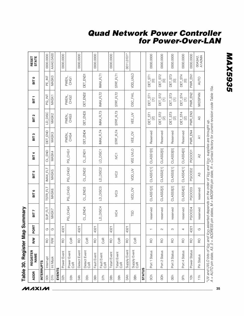
MA
X5
93
5
Quad Network Power Controllerfor Power-Over-LAN
______________________________________________________________________________________ 35
Tab
le 3
0. R
egis
ter
Map
Su
mm
ary
AD
DR
RE
GIS
TE
RN
AM
ER
/WP
OR
TB
IT 7
BIT
6B
IT 5
BIT
4B
IT 3
BIT
2B
IT 1
BIT
0R
ES
ET
ST
AT
E
INT
ER
RU
PT
S
00h
Inte
rrup
tR
OG
SU
P_F
LTTS
TR_F
LTIM
AX
_FLT
CL_
EN
DD
ET_
EN
DLD
_DIS
CP
G_I
NT
PE
_IN
T00
00,0
000
01h
Int M
ask
R/W
GM
AS
K7
MA
SK
6M
AS
K5
MA
SK
4M
AS
K3
MA
SK
2M
AS
K1
MA
SK
0A
AA
0,0A
00
EV
EN
TS
02h
Pow
er E
vent
RO
4321
0000
,000
0
03h
Pow
er E
vent
CoR
CoR
PG
_CH
G4
PG
_CH
G3
PG
_CH
G2
PG
_CH
G1
PW
EN
_C
HG
4P
WE
N_
CH
G3
PW
EN
_C
HG
2P
WE
N_
CH
G1
04h
Det
ect E
vent
RO
4321
0000
,000
0
05h
Det
ect E
vent
CoR
CoR
CL_
EN
D4
CL_
EN
D3
CL_
EN
D2
CL_
EN
D1
DET
_EN
D4
DET
_EN
D3
DET
_EN
D2
DET
_EN
D1
06h
Faul
t Eve
ntR
O43
2100
00,0
000
07h
Faul
t Eve
ntC
oRC
oRLD
_DIS
C4
LD_D
ISC
3LD
_DIS
C2
LD_D
ISC
1IM
AX_F
LT4
IMAX
_FLT
3IM
AX_F
LT2
IMAX
_FLT
1
08h
Tsta
rt E
vent
RO
4321
0000
,000
0
09h
Tsta
rt E
vent
CoR
CoR
IVC
4IV
C3
IVC
2IV
C1
STRT
_FLT
4ST
RT_F
LT3
STRT
_FLT
2ST
RT_F
LT1
0Ah
Sup
ply
Eve
ntR
O43
2100
11,0
101*
0Bh
Sup
ply
Eve
ntC
oRC
oRTS
DV
DD
_OV
VD
D_U
VV
EE
UV
LOV
EE
_OV
VE
E_U
VO
SC
_FA
ILVD
D_U
VLO
ST
AT
US
0Ch
Por
t 1 S
tatu
sR
O1
rese
rved
CLA
SS
1[2]
CLA
SS
1[1]
CLA
SS
1[0]
Res
erve
dD
ET_
ST1
[2]
DE
T_S
T1[1
]D
ET_
ST1
[0]
0000
,000
0
0Dh
Por
t 2 S
tatu
sR
O2
rese
rved
CLA
SS
2[2]
CLA
SS
2[1]
CLA
SS
2[0]
Res
erve
dD
ET_
ST2
[2]
DE
T_S
T2[1
]D
ET_
ST2
[0]
0000
,000
0
0Eh
Por
t 3 S
tatu
sR
O3
rese
rved
CLA
SS
3[2]
CLA
SS
3[1]
CLA
SS
3[0]
Res
erve
dD
ET_
ST3
[2]
DE
T_S
T3[1
]D
ET_
ST3
[0]
0000
,000
0
0Fh
Por
t 4 S
tatu
sR
O4
rese
rved
CLA
SS
4[2]
CLA
SS
4[1]
CLA
SS
4[0]
Res
erve
dD
ET_
ST4
[2]
DE
T_S
T4[1
]D
ET_
ST4
[0]
0000
,000
0
10h
Pow
er S
tatu
sR
O43
21P
GO
OD
4P
GO
OD
3P
GO
OD
2P
GO
OD
1P
WR
_EN
4P
WR
_EN
3P
WR
_EN
2P
WR
_EN
100
00,0
000
11h
Pin
Sta
tus
RO
Gre
serv
edre
serv
edA
3A
2A
1A
0M
IDS
PA
NA
UTO
00A
3A2,
A1A
0MA
*UV
and
UV
LO b
its o
f VE
Ean
d V
DD
asse
rted
dep
end
s on
the
ord
er o
f VE
E a
nd V
DD
su
pp
lies
are
bro
ught
up
.A
= A
UTO
pin
sta
te, A
3..0
= A
DD
RE
SS
pin
sta
tes,
M =
MID
SP
AN
pin
sta
te, R
= C
onta
ct fa
ctor
y fo
r cu
rren
t rev
isio
n co
de
Tab
le 1
5a.

MA
X5
93
5
Quad Network Power Controllerfor Power-Over-LAN
36 ______________________________________________________________________________________
Tab
le 3
0. R
egis
ter
Map
Su
mm
ary
(co
nti
nu
ed)
AD
DR
RE
GIS
TE
RN
AM
ER
/WP
OR
TB
IT 7
BIT
6B
IT 5
BIT
4B
IT 3
BIT
2B
IT 1
BIT
0R
ES
ET
ST
AT
E
CO
NF
IGU
RA
TIO
N
12h
Op
erat
ing
Mod
eR
/W43
21P
4_M
1P
4_M
0P
3_M
1P
3_M
0P
2_M
1P
2_M
0P
1_M
1P
1_M
0A
AAA
,AAA
A
13h
Dis
conn
ect
Ena
ble
R/W
4321
AC
D_E
N4
AC
D_E
N3
AC
D_E
N2
AC
D_E
N1
DC
D_E
N4
DC
D_E
N3
DC
D_E
N2
DC
D_E
N1
0000
,AA
AA
14h
Det
/Cla
ssE
nab
leR
/W43
21C
LAS
S_E
N4
CLA
SS
_EN
3C
LAS
S_E
N2
CLA
SS
_EN
1D
ET_
EN
4D
ET_
EN
3D
ET_
EN
2D
ET_
EN
1A
AAA
,AAA
A
15h
Bac
koff
Ena
ble
R/W
4321
rese
rved
rese
rved
rese
rved
rese
rved
Bck
off4
Bck
off3
Bck
off2
Bck
off1
0000
,MM
MM
16h
Tim
ing
Con
figR
/WG
RS
TR[1
]R
STR
[0]
TSTA
RT[
1]
TSTA
RT[
0]
TFAU
LT[1
] TF
AULT
[0]
TDIS
C[1
]TD
ISC
[0]
0000
,000
0
17h
Mis
c C
onfig
R/W
GIN
T_E
NR
STR
_EN
rese
rved
rese
rved
PO
FF_C
LC
L_D
ISC
rese
rved
rese
rved
1100
,000
0
PU
SH
BU
TT
ON
S
18h
Res
erve
dR
/WG
rese
rved
rese
rved
rese
rved
rese
rved
rese
rved
rese
rved
rese
rved
rese
rved
19h
Pow
er E
nab
leW
O43
21PW
R_O
FF4
PWR_
OFF
3PW
R_O
FF2
PWR_
OFF
1P
WR
_ON
4P
WR
_ON
3P
WR
_ON
2P
WR
_ON
100
00,0
000
1Ah
Glo
bal
WO
GC
LR_I
NT
rese
rved
rese
rved
RE
SE
T_IC
RE
SE
T_P
4R
ES
ET_
P3
RE
SE
T_P
2R
ES
ET_
P1
0000
,000
0
GE
NE
RA
L
1Bh
IDR
OG
ID_C
OD
E[ 4]
ID_C
OD
E[ 3]
ID_C
OD
E[ 2]
ID_C
OD
E[ 1]
ID_C
OD
E[ 0]
RE
V [
2]R
EV
[1]
RE
V [
0]11
00,0
RR
R
1Ch
SM
OD
EC
oR43
21re
serv
edre
serv
edre
serv
edre
serv
edS
MO
DE
4S
MO
DE
3S
MO
DE
2S
MO
DE
100
0000
00
1Dh
Res
erve
dG
rese
rved
rese
rved
rese
rved
rese
rved
Res
erve
dre
serv
edre
serv
edre
serv
ed00
0000
00
1EH
Wat
chd
ogR
/WG
WD
TIM
E[7
]2]
WD
TIM
E[6
]W
D TI
ME [
5]W
DTI
ME
[4]
WD
TIM
E[3
]W
DTI
ME
[2]
WD
TIM
E[1
]W
DTI
ME
[0]
0000
0000
1FH
Sw
itch
Mod
eR
/W43
21EN
_ WH
DO
GW
D_I
NT_
ENre
serv
edA
CTE
ST
HW
MO
DE
4H
WM
OD
E3
HW
MO
DE
2H
WM
OD
E1
0000
0000
MA
XIM
RE
SE
RV
ED
20H
Res
erve
dG
rese
rved
rese
rved
rese
rved
rese
rved
Res
erve
dre
serv
edre
serv
edre
serv
ed00
0000
00
21H
Res
erve
dG
rese
rved
rese
rved
rese
rved
rese
rved
Res
erve
dre
serv
edre
serv
edre
serv
ed00
0000
00
22H
Res
erve
dG
rese
rved
rese
rved
rese
rved
rese
rved
Res
erve
dre
serv
edre
serv
edre
serv
ed00
0000
00
23H
Pro
gra
m1
R/W
4321
IGA
TE[2
]IG
ATE
[1]
IGA
TE[0
]D
ET_
BY
PO
SC
F_R
SA
C_T
H[0
]A
C_T
H[0
]A
C_T
H[0
]00
0001
00
24h
Res
erve
dG
rese
rved
rese
rved
rese
rved
rese
rved
Res
erve
dre
serv
edre
serv
edre
serv
ed00
0000
00
25h
Res
erve
dG
rese
rved
rese
rved
rese
rved
rese
rved
Res
erve
dre
serv
edre
serv
edre
serv
ed00
0000
00
26h
Res
erve
dG
rese
rved
rese
rved
rese
rved
rese
rved
Res
erve
dre
serv
edre
serv
edre
serv
ed00
0000
00
27H
Pro
gra
m2
R/W
GIM
AX
[3]
IMA
X[2
]IM
AX
[1]
IMA
X[0
]TD
[3]
TD[2
]TD
[1]
TD[0
]01
0001
11
28H
Pro
gra
m3
R/W
GTF
_PR
[3]
TF_P
R[2
]TF
_PR
[1]
TF_P
R[0
]TS
_PR
[3]
TS_P
R[2
]TS
_PR
[1]
TS_P
R[0
]01
1101
11
*UV
and
UV
LO b
its o
f VE
Ean
d V
DD
asse
rted
dep
end
s on
the
ord
er o
f VE
E a
nd V
DD
su
pp
lies
are
bro
ught
up
.A
= A
UTO
pin
sta
te, A
3..0
= A
DD
RE
SS
pin
sta
tes,
M =
MID
SP
AN
pin
sta
te, R
= C
onta
ct fa
ctor
y fo
r cu
rren
t rev
isio
n co
de
Tab
le 1
5a.
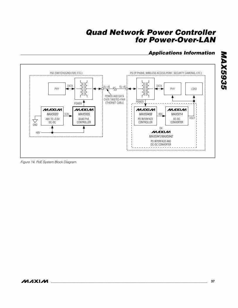
MA
X5
93
5
Quad Network Power Controllerfor Power-Over-LAN
______________________________________________________________________________________ 37
Figure 14. PoE System Block Diagram
MAX5935QUAD PoE
CONTROLLER
MAX5020-48V TO +3.3V
DC-DC
MAX5940BPD INTERFACECONTROLLER
MAX5014DC-DC
CONVERTERGND
-48V
PHYDATA
PHY LOADDATA
POWER
3.3V -48V
POWER
MAX5941/MAX5942PD INTERFACE ANDDC-DC CONVERTER
OR
PSE (SWITCHES/ROUTER, ETC.) PD (IP PHONE, WIRELESS ACCESS POINT, SECURITY CAMERAS, ETC.)
RJ–45RJ–45
POWER AND DATAOVER TWISTED-PAIR
ETHERNET CABLE
VOUT
Applications Information

MA
X5
93
5
Quad Network Power Controllerfor Power-Over-LAN
38 ______________________________________________________________________________________
Figure 15. PoE System Diagram of One Complete Port, Endpoint PSE
MAX5935
-48V
GATE_
INTERNAL PULLDOWN(MANUAL MODE)
1kΩ
-48VRTN
FDT3612100V, 120mΩ
SOT-223
SENSE_VEE OUT_
OFF
ON
DET_
SDAIN
SDAOUT
SCL
DGND
VDDA0 A1 A2 A3
OSC_IN
AUTO
MIDSPAN
AGND
INTERNAL PULLDOWN(SIGNAL MODE)
0.5Ω1%
1N4448
1kΩ
1 OF 4 CHANNELS
1.8V TO 5V,(REF TO DGND)
INT
RESET
3kΩ
3kΩ
180Ω
180Ω
180Ω
OPTIONAL BUFFER
INTERNAL50kΩ PULLUP 4.7kΩ
1kΩ
VDD
1N4002
HPCL063L
OPTIONAL BUFFER
OPTIONAL BUFFER
HPCL063L
HPCL063L
VCCRTN
VCC (3.3V)
SCL
SDA
SERI
AL IN
TERF
ACE
3kΩ
3kΩ
ISOLATION
0.47µF100V
SHD_
SINE WAVE100Hz ±10%PEAK AMPLITUDE 2.2V ±0.1VVALLEY AMPLITUDE 0.2V ±0.1V
SMBJ58CA 0.1µF 2.2MΩ
-48VOUT
8
7
5
4
6
3
2
1
-48VOUT
0.1µF
0.1µF
0.1µF
0.1µF75Ω
75Ω 75Ω
75Ω
1000pF250VAC
24
22
21
19
23
20
RX1+
RX1-
TX1+
TX1-
RXT1
TXCT1
RD1+
RD1-
TD1+
TD1-
1
3
4
5
PHY1/2 OF
H2005A
RJ–45CONNECTOR

MA
X5
93
5
Quad Network Power Controllerfor Power-Over-LAN
______________________________________________________________________________________ 39
Figure 16. PoE System Diagram of One Complete Port, Midspan PSE
MAX5935
-48V
GATE_
INTERNAL PULLDOWN(MANUAL MODE)
1kΩ
-48VRTN
FDT3612100V, 120mΩ
SOT-223
SENSE_VEE OUT_
OFF
ON
DET_
SDAIN
SDAOUT
SCL
DGND
VDDA0 A1 A2 A3
OSC_IN
AUTO
MIDSPAN
AGND
INTERNAL PULLDOWN(SIGNAL MODE)
0.5Ω1%
1N4448
1kΩ
1 OF 4 CHANNELS
1.8V TO 5V(REF TO DGND)
INT
RESET
3kΩ
3kΩ
180Ω
180Ω
180Ω
OPTIONAL BUFFER
INTERNAL50kΩ PULLUP 4.7kΩ
1kΩ
VDD
1N4002
HPCL063L
OPTIONAL BUFFER
OPTIONAL BUFFER
HPCL063L
HPCL063L
VCCRTN
VCC (3.3V)
SCL
SDA
SERI
AL IN
TERF
ACE
3kΩ
3kΩ
ISOLATION
0.47µF100V
SHD_
SINE WAVE100Hz ±10%PEAK AMPLITUDE 2.2V ±0.1VVALLEY AMPLITUDE 0.2V ±0.1V
SMBJ58CA 0.1µF 2.2MΩ
-48VOUT
8
7
5
4
6
3
2
1
RJ–45CONNECTOR
-48VOUT
DATA

MA
X5
93
5
Quad Network Power Controllerfor Power-Over-LAN
40 ______________________________________________________________________________________
Figure 17. -48V to +3.3V (300mA) Boost Converter Solution for VDIG
GND
-48V-48V
GND
C60.47µF
100V
R102Ω
R61Ω
C315nF
Q4MMBTA56
R51kΩ
L168µH, DO3308P-683
MAX50201
2
3
4
8
7
6
5
V+
VDD
FB
VCC
NDRV
GND
CS
C20.022µF
R830Ω
C10.1µF
C82.2µF
R41Ω
R91Ω
GATE
SOURCE
DRAIN
Q1Si2328 DS
C94.7µH
C70.22µF
R71.02kΩ
R26.81kΩ
R32.61kΩ
Q3MMBTA56
D1DIODES INC.: B1100
C4220µF
Sanyo 6SPS220M
R12.6kΩ
Q2MMBTA56
C54.7µF
+3.3V+3.3V
GND
300mA
SS_SHDN
Figure 18. Layout Example for Boost Converter Solution for VDIG
1700 (mil)
965
(mil)
1700 (mil)
965
(mil)
1700 (mil)
965
(mil)

MA
X5
93
5
Quad Network Power Controllerfor Power-Over-LAN
______________________________________________________________________________________ 41
DESIGNATION DESCRIPTION
C1 0.1µF, 25V ceramic capacitor
C2 0.022µF, 25V ceramic capacitor
C3 15nF, 25V ceramic capacitor
C4220µF capacitorSanyo 6SVPA220MAA
C5 4.7µF, 16V ceramic capacitor
C6 0.1µF, 100V ceramic capacitor
C7 0.22µF, 16V ceramic capacitor
C8 0.22µF, 16V ceramic capacitor
C9 4.7nF, 16V ceramic capacitor
D1 B1100 100V Schottky diode
L168µH inductorCoilcraft DO3308P-683 or equivalent
Q1Si2328DSVishay n-Channel MOSFET, SOT-23
Q2 MMBTA56 small-signal pnp
Q3 MMBTA56 small-signal pnp
Q4 MMBTA56 small-signal pnp
R1 2.61kΩ ±1% resistor
R2 6.81kΩ ±1% resistor
R3 2.61kΩ ±1% resistor
R4 1Ω ±1% resistor
R5 1kΩ ±1% resistor
R6 1Ω ±1% resistor
R7 1.02kΩ ±1% resistor
R8 30Ω ±1% resistor
R9 1Ω ±1% resistor
R10 2Ω ±1% resistor
U1High-voltage PWM ICMAX5020ESA (8-pin SO)
Component List Chip InformationTRANSISTOR COUNT: 148,768
PROCESS: BiCMOS

MA
X5
93
5
Quad Network Power Controllerfor Power-Over-LAN
42 ______________________________________________________________________________________
MAX5935
-48V
GATE_
INTERNAL PULLDOWN(MANUAL MODE)
1kΩ
-48VRTN
FDT3612100V, 120mΩ
SOT-223
SENSE_VEE OUT_
OFF
ON
DET_
SDAIN
SDAOUT
SCL
DGND
VDDA0 A1 A2 A3
OSC_IN
AUTO
MIDSPAN
AGND
INTERNAL PULLDOWN(SIGNAL MODE)
0.5Ω1%
-48VOUTPUT TO
PORT
-48V RTNOUTPUT TO PORT
NOTE: ALL SIGNAL PINS ARE REFERENCED TO DGND. DGND RANGE IS BETWEEN VEE AND (AGND + 4V).
1N4448
1 OF 4 CHANNELS
1.8V TO 3.7V,(REF TO DGND)
INT
RESET
3kΩ
3kΩ
180Ω
180Ω
180Ω
OPTIONAL BUFFER
INTERNAL50kΩ PULLUP 4.7kΩ
1kΩ
VDD
CAN BE UP TO 100kΩ
HPCL063L
OPTIONAL BUFFER
OPTIONAL BUFFER
HPCL063L
HPCL063L
VCCRTN
VCC (3.3V)
SCL
SDA
SERI
AL IN
TERF
ACE
3kΩ
3kΩ
ISOLATION
N.C.
SHD_
Typical Operating Circuits
Typical Operating Circuit 1 (without AC Load Removal Detection)

MA
X5
93
5
Quad Network Power Controllerfor Power-Over-LAN
______________________________________________________________________________________ 43
MAX5935
-48V
GATE_
INTERNAL PULLDOWN(MANUAL MODE)
1kΩ
-48VRTN
FDT3612100V, 120mΩ
SOT-223
SENSE_VEE OUT_
OFF
ON
DET_
SDAIN
SDAOUT
SCL
DGND
VDDA0 A1 A2 A3
OSC_IN
AUTO
MIDSPAN
AGND
INTERNAL PULLDOWN(SIGNAL MODE)
0.5Ω1%
-48VOUTPUT TO
PORT
-48V RTNOUTPUT TO PORT
NOTE: ALL SIGNAL PINS ARE REFERENCED TO DGND.
1N4448
1kΩ
1 OF 4 CHANNELS
1.8V TO 3.7V,(REF TO DGND)
INT
RESET
3kΩ
3kΩ
180Ω
180Ω
180Ω
OPTIONAL BUFFER
INTERNAL50kΩ PULLUP 4.7kΩ
1kΩ
VDD
1N4002
CAN BE UP TO 100kΩ
HPCL063L
OPTIONAL BUFFER
OPTIONAL BUFFER
HPCL063L
HPCL063L
VCCRTN
VCC (3.3V)
SCL
SDA
SERI
AL IN
TERF
ACE
3kΩ
3kΩ
ISOLATION
DGND MUST BE CONNECTED DIRECTLY TO AGND FOR AC DISCONNECT DETECTION CIRCUIT TO OPERATE.
0.47µF100V
SHD_
SINE WAVE100Hz ±10%PEAK AMPLITUDE 2.2V ±0.1VVALLEY AMPLITUDE 0.2V ±0.1V
Typical Operating Circuits (continued)
Typical Operating Circuit 2 (with AC Load Removal Detection)
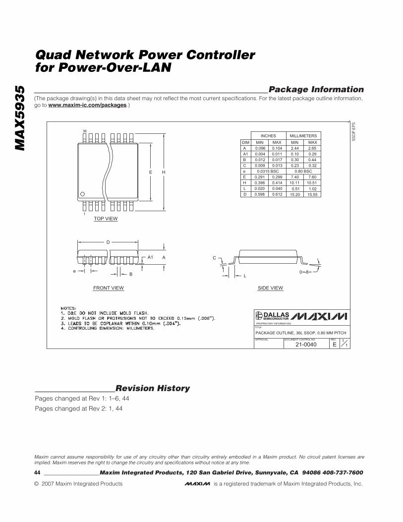
MA
X5
93
5
Quad Network Power Controllerfor Power-Over-LAN
Maxim cannot assume responsibility for use of any circuitry other than circuitry entirely embodied in a Maxim product. No circuit patent licenses areimplied. Maxim reserves the right to change the circuitry and specifications without notice at any time.
44 ____________________Maxim Integrated Products, 120 San Gabriel Drive, Sunnyvale, CA 94086 408-737-7600
© 2007 Maxim Integrated Products is a registered trademark of Maxim Integrated Products, Inc.
Package Information(The package drawing(s) in this data sheet may not reflect the most current specifications. For the latest package outline information,go to www.maxim-ic.com/packages.)
SS
OP
.EP
S
PACKAGE OUTLINE, 36L SSOP, 0.80 MM PITCH
11
21-0040 EREV.DOCUMENT CONTROL NO.APPROVAL
PROPRIETARY INFORMATIONTITLE:
FRONT VIEW
MAX
0.0110.104
0.017
0.299
0.013
INCHES
0.291
0.009
E
C
DIM
0.0120.004
BA1
MIN0.096A
0.23
7.40 7.60
0.32
MILLIMETERS
0.100.30
2.44MIN
0.440.29
MAX2.65
0.0400.020L 0.51 1.02H 0.4140.398 10.11 10.51
e 0.0315 BSC 0.80 BSC
D 0.6120.598 15.20 15.55
HE
A1 A
D
eB 0∞-8∞
L
C
TOP VIEW
SIDE VIEW
1
36
Revision HistoryPages changed at Rev 1: 1–6, 44
Pages changed at Rev 2: 1, 44