proximity-induced magnetization in graphene: towards
TRANSCRIPT

University of Nebraska - Lincoln University of Nebraska - Lincoln
DigitalCommons@University of Nebraska - Lincoln DigitalCommons@University of Nebraska - Lincoln
Kirill Belashchenko Publications Research Papers in Physics and Astronomy
11-13-2020
Proximity-induced magnetization in graphene: Towards efficient Proximity-induced magnetization in graphene: Towards efficient
spin gating spin gating
Mihovil Bosnar Institute Ruder Boskovic, [email protected]
Ivor Lončarić Institute Ruder Boskovic
P. Lazić Institute Ruder Boskovic
Kirill Belashchenko University of Nebraska - Lincoln, [email protected]
Igor Žutić University at Buffalo, The State University of New York
Follow this and additional works at: https://digitalcommons.unl.edu/physicsbelashchenko
Part of the Atomic, Molecular and Optical Physics Commons, Condensed Matter Physics Commons,
Engineering Physics Commons, Other Materials Science and Engineering Commons, and the Statistical,
Nonlinear, and Soft Matter Physics Commons
Bosnar, Mihovil; Lončarić, Ivor; Lazić, P.; Belashchenko, Kirill; and Žutić, Igor, "Proximity-induced magnetization in graphene: Towards efficient spin gating" (2020). Kirill Belashchenko Publications. 38. https://digitalcommons.unl.edu/physicsbelashchenko/38
This Article is brought to you for free and open access by the Research Papers in Physics and Astronomy at DigitalCommons@University of Nebraska - Lincoln. It has been accepted for inclusion in Kirill Belashchenko Publications by an authorized administrator of DigitalCommons@University of Nebraska - Lincoln.
PHYSICAL REVIEW MATERIALS 4, 114006 (2020)
Proximity-induced magnetization in graphene: Towards efficient spin gating
Mihovil Bosnar ,1,* Ivor Loncaric ,1,† P. Lazic,2,1 K. D. Belashchenko ,3 and Igor Žutic4
1Ruđer Boškovic Institute, 10000 Zagreb, Croatia2Research Computing Support Services Group, University of Missouri, Columbia, Missouri 65211-7010, USA
3University of Nebraska-Lincoln and Nebraska Center for Materials and Nanoscience, Lincoln, Nebraska 68588-0299, USA4University at Buffalo, State University of New York, Buffalo, New York 14260-1500, USA
(Received 14 February 2020; revised 14 September 2020; accepted 29 October 2020; published 13 November 2020)
Gate-tunable spin-dependent properties could be induced in graphene at room temperature through themagnetic proximity effect by placing it in contact with a metallic ferromagnet. Because strong chemical bondingwith the metallic substrate makes gating ineffective, an intervening passivation layer is needed. Previouslyconsidered passivation layers result in a large shift of the Dirac point away from the Fermi level, so thatunrealistically large gate fields are required to tune the spin polarization in graphene (Gr). We show that amonolayer of Au or Pt used as the passivation layer between Co and graphene brings the Dirac point closerto the Fermi level. In the Co/Pt/Gr system the proximity-induced spin polarization in graphene and its gatecontrol are strongly enhanced by the presence of a surface band near the Fermi level. Furthermore, the shift ofthe Dirac point could be eliminated entirely by selecting submonolayer coverage in the passivation layer. Ourfindings open a path towards experimental realization of an optimized two-dimensional system with gate-tunablespin-dependent properties.
DOI: 10.1103/PhysRevMaterials.4.114006
I. INTRODUCTION
With its high mobility and low spin-orbit coupling,graphene (Gr) is expected to be a particularly suitable ma-terial for spin transport and spintronics [1–3]. From the firstdemonstration of spin injection in graphene [4], there has beensignificant progress in extending the characteristic time andlength scales over which spin information can be sustained[5,6]. Graphene-based spin-logic gates have been demon-strated at room temperature [7], supporting proposals forspecialized applications that could outperform complemen-tary metal oxide semiconductor (CMOS)-based counterparts[8].
Despite its attractive intrinsic properties, there is a stronginterest in introducing superconductivity, magnetism, a siz-able energy gap, topological properties, or strong spin-orbitcoupling into graphene. Chemical doping or functionalizationtend to introduce unwanted disorder and significantly reducethe mobility of charge carriers in graphene [9]. However, theatomic thickness of graphene and other two-dimensional (2D)materials offers an alternative way to modify their propertiesthrough short-range proximity effects [9] from an adjacentlayer that already has the desired properties [10–16].
Interest in magnetic proximity effects in 2D systems isexceedingly broad, as they are considered for implementingmagnetic skyrmions [17], exotic properties of topologicalinsulators [18], and Majorana bound states for topologicalquantum computing [19–22]. In this paper we focus on mag-
*[email protected]†[email protected]
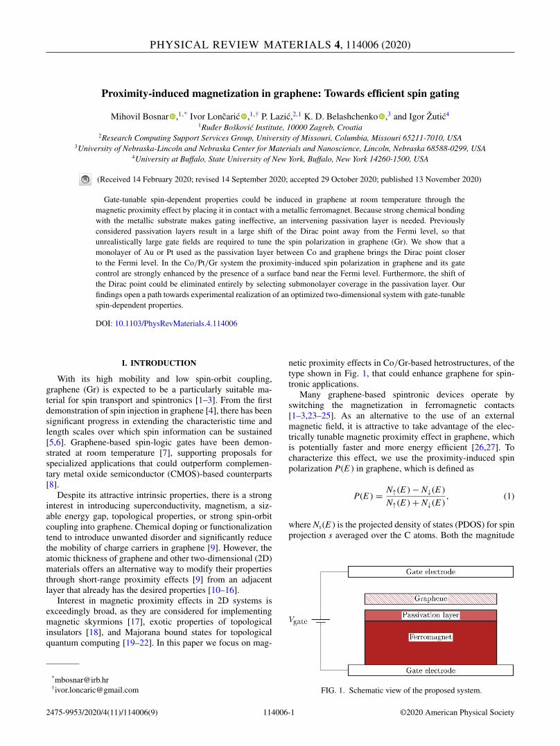
netic proximity effects in Co/Gr-based hetrostructures, of thetype shown in Fig. 1, that could enhance graphene for spin-tronic applications.
Many graphene-based spintronic devices operate byswitching the magnetization in ferromagnetic contacts[1–3,23–25]. As an alternative to the use of an externalmagnetic field, it is attractive to take advantage of the elec-trically tunable magnetic proximity effect in graphene, whichis potentially faster and more energy efficient [26,27]. Tocharacterize this effect, we use the proximity-induced spinpolarization P(E ) in graphene, which is defined as
P(E ) = N↑(E ) − N↓(E )
N↑(E ) + N↓(E ), (1)
where Ns(E ) is the projected density of states (PDOS) for spinprojection s averaged over the C atoms. Both the magnitude
FIG. 1. Schematic view of the proposed system.
2475-9953/2020/4(11)/114006(9) 114006-1 ©2020 American Physical Society
MIHOVIL BOSNAR et al. PHYSICAL REVIEW MATERIALS 4, 114006 (2020)
and the sign of P(E ) near the Fermi level EF can be controlledby electric gating [26].
It is usually expected that tunable magnetic proximity ef-fects require a magnetic insulator to avoid shorting the circuitthrough the metallic ferromagnet [28–33]. Indeed, grapheneforms strong chemical bonds with Co and Ni [26,34,35],which essentially turns it into a metallic continuation of theferromagnet with a large density of states (DOS) at the Fermilevel. As a result, it is practically impossible to change P(EF )in such chemisorbed graphene by electric gating [26].
Therefore, the idea to select heterostructures with a van derWaals (vdW) bonded layer of graphene was introduced [26].A common metallic ferromagnet with a high Curie tempera-ture could then be considered for tunable magnetic proximityeffects. In particular, surface passivation through an additionof another graphene layer [26] or a layer of hexagonal boronnitride (h-BN) [26,34] between graphene and Co, as shown inFig. 1, was studied. In both cases passivation results in weakvdW bonding of the top layer of graphene to the underlyingstructure [26].
Weak vdW bonding tends to preserve major features ofthe electronic structure, such as the Dirac cone in graphene[26,35,36], but the bound system still has important differ-ences compared to its stand-alone components. In systemsstudied previously, the most relevant features are (n-type) dop-ing [26,35] and lifting of the spin degeneracy in graphene dueto the proximity effect [26,34]. This proximity effect has beenutilized in transport experiments [36] aiming to use graphenenot as a spin filter (as in the tunneling geometry [37]) but as asource of spin-polarized carriers.
Graphene and the passivated surface can be thought of astwo plates of a capacitor. The gate voltage Vgate induces anelectrostatic potential difference and charge transfer betweenthese plates, which can change P(EF ) in graphene and some-times even its sign [26]. The potential difference dependsinversely on the DOS at the Fermi level in graphene [26]. Itis, therefore, expected that P(EF ) should be more sensitive togating if the Fermi level is close to the Dirac point.
With h-BN and graphene passivation layers on the surfaceof Co, physisorbed graphene is n-doped with its Dirac pointshifted approximately 0.5 eV below the Fermi level and arelatively large DOS at the Fermi level [26]. First-principlescalculations have shown that significant tuning of P(E ) in thissystem requires large electric fields [26] that are achievableonly by ionic-liquid gating [39,40]. This conclusion was cor-roborated by experiments on lateral Co/h-BN/Gr-based spinvalves [41], where electrostatic gating failed to produce tun-able magnetic proximity effects in 2D ferromagnetic contactsin the planar geometry similar to that in Fig. 1. Instead, toreduce detrimental n-doping, one-dimensional edge contactswere used to achieve the ability to switch the proximity-induced spin polarization in graphene by gating [41].
In this paper we explore a different path to realizing tun-able spin polarization in 2D geometry by using a monolayerof noble-metal atoms like Au or Pt as the passivation layerbetween the Co surface and graphene. Furthermore, we showthat additional flexibility can be achieved by using a passi-vation layer with a variable partial coverage. In fact, a studyof graphene doping on Au-passivated Ni surface found thatreducing the coverage of Ni by Au atoms reduces the doping
level in graphene [42]. Our first-principles calculations basedon these considerations provide useful guidance for realiz-ing proximity-induced spin polarization and spin gating ingraphene.
While doping of graphene is not eliminated in any of thestructures studied here, all of them have more than an orderof magnitude larger P(EF ) at electric fields under 0.1 V/Åcompared to Co/h-BN/Gr heterostructures, reaching 15%with Pt-passivated Co. Furthermore, doping in 100% coveredstructures is p-type, in contrast to n-type in the Co/h-BN/Grstructure, while the reduction in coverage drastically shifts thedoping level towards n-type for both Au- and Pt-passivatedCo. This result suggests a way to design the desired structurewhere doping is entirely canceled.
II. COMPUTATIONAL DETAILS
Proximity-induced spin polarization in graphene was stud-ied using density functional theory (DFT) as implementedin a real-space code GPAW [43–45]. The real-space approachavoids the use of periodic boundary conditions in the non-periodic direction, preventing spurious tunneling [26] andobviating the need for dipole interaction corrections [46].
We used projector-augmented-wave [47,48] Perdue-Burke-Ernzerhof [49] setups from the GPAW package and thesemilocal vdW functional vdw-df-cx [50–52] from the libvd-wxc library [53] for exchange and correlation. The cell wassampled by a grid of 0.133 (0.129) Å spacing in the planesparallel (perpendicular) to the heterostructure layers.
Input structures were constructed in QuantumWiseVIRTUAL NANOLAB [54]. For the fully covered hexagonalclose-packed Co(0001) surface we used a slab with sevenlayers of Co atoms. The passivating Au or Pt monolayerswere added in an extension of this slab, fully covering thesurface and forming a 1 × 1 supercell. Since the experimentallattice constants of graphene (2.461 Å) and Co(0001) surface(2.507 Å) make a small lattice mismatch of 1.8%, we useda 1 × 1 supercell with the lattice parameter of graphene. Allsupercells contained 10 Å of vacuum on both sides of theheterostructure.
To find the optimal lateral position of graphene, we relaxedthe system starting from three configurations: Au or Pt atomlocated under the hollow site of graphene, under a C–C bond,and under a C atom. Relaxations were performed using thequasi-Newton algorithm, as implemented in the ASE package[45], with GPAW as the DFT calculator, until the force oneach atom was smaller than 0.05 eV/Å. We fixed the bottomtwo layers of Co and used a 15 × 15 × 1 Monkhorst-Packsampling of the Brillouin zone with a Fermi-Dirac smearingof 200 meV.
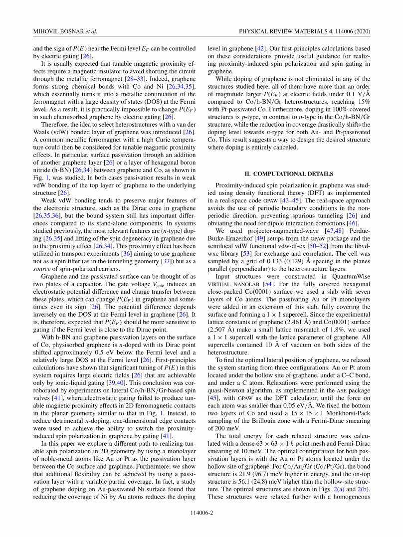
The total energy for each relaxed structure was calcu-lated with a dense 63 × 63 × 1 k-point mesh and Fermi-Diracsmearing of 10 meV. The optimal configuration for both pas-sivation layers is with the Au or Pt atoms located under thehollow site of graphene. For Co/Au/Gr (Co/Pt/Gr), the bondstructure is 21.9 (96.7) meV higher in energy, and the on-topstructure is 56.1 (24.8) meV higher than the hollow-site struc-ture. The optimal structures are shown in Figs. 2(a) and 2(b).These structures were relaxed further with a homogeneous
114006-2

PROXIMITY-INDUCED MAGNETIZATION IN GRAPHENE: … PHYSICAL REVIEW MATERIALS 4, 114006 (2020)
FIG. 2. Top (a) [(c)] and side (b) [(d)] view of the optimal energy structure with 100% [75%] Co surface coverage by Pt or Au. C atoms areshown in dark blue, noble metal in yellow, and Co in light blue. Two inequivalent C atoms in the case of 100% coverage are marked by 1 and2. The listed average interlayer distances correspond to equilibrium without the applied field. This figure was made using XCRYSDEN software[38].
electric field of Ez = ±0.01, ±0.05, ±0.1, and ±0.2 V/Å,applied perpendicular to the surface.
As a case study of a system with lower coverage in thepassivation layer, we used a system with a 75% covered Cosurface shown in Figs. 2(c) and 2(d). To obtain the 75%coverage, three atoms of Au or Pt were placed on the 2 × 2supercell of Co(0001). The starting positions were taken fromRef. [42] for the Ni(111)/Au/Gr system. Instead of seven Colayers used for the full coverage, here we used five Co layersto keep the calculation manageable; the system was relaxedwith the same procedure.
We used finer Brilloiun zone sampling and Fermi-Diracsmearing of 10 meV for the precise calculation of the mag-netic moments. For systems with 100% (75%) coverage weused a 111 × 111 × 1 (32 × 32 × 1) k-point mesh, whichwas also used to calculate the spin-resolved PDOS where200-meV Gaussian broadening was chosen.
The atomic magnetic moments were estimated as the in-tegrals of the spin density S , defined as the difference ofelectronic densities ρ in the two spin channels,
S (r) = ρ↑(r) − ρ↓(r), (2)
over the augmentation spheres.
III. RESULTS AND DISCUSSION
A. Zero gate voltage
The band structures of the Co/Au/Gr and Co/Pt/Gr sys-tems with 100% coverage in the passivation layer, at zero
applied field, are shown in Fig. 3. In both cases the Diraccone of graphene is preserved but shifted to higher en-ergies by 0.33 and 0.22 eV for Pt and Au, respectively.Along with the distances of about 3.5 Å between grapheneand the Pt or Au layer (see Fig. 2), these results suggestvdW bonding between graphene and the metallic surface.Graphene here is p-doped to a lesser extent compared ton-doped graphene in the system with a h-BN passivationlayer [26].
A closer look at the band structure near the Fermi levelshown in the insets in Figs. 3(a) and 3(b) reveals that spinsplitting is induced in graphene in both systems. In Co/Au/Grthe splitting is approximately constant near the Fermi leveland we estimate it to be about 1.05 meV. This splitting rep-resents interlayer exchange [34]. In contrast, in Co/Pt/Grthe splitting varies sharply near the Fermi level due to thehybridization of the graphene and flat metal bands and theensuing avoided band crossings. We note that avoided cross-ings are also present in Co/Au/Gr and exchange splitting ispresent in Co/Pt/Gr, but their effect on the respective bandstructures appears to be smaller.
The magnetic proximity effect induces a finite spin densityS in graphene. Figure 4 shows a planar slice of S (r) ata distance of 0.33 Å above the carbon nuclei. Clearly, thespin density is inhomogeneous in both systems, reflecting theinhomogeneity of the surface. Furthermore, the spin density inCo/Au/Gr has different signs on the two inequivalent carbonatoms.
To gain insight into how S is formed from the band contri-butions, one can integrate the difference in PDOS Na,s(E ) on
114006-3

MIHOVIL BOSNAR et al. PHYSICAL REVIEW MATERIALS 4, 114006 (2020)
FIG. 3. The band structure of (a) Co/Au/Gr and (b) Co/Pt/Gr for full coverage in the passivation layer. Insets: Enlarged portion of theband structure near the Fermi level.
a C atom of type a up to some energy E0:
Da(E0) =∫ E0
−∞[Na,↑(E ) − Na,↓(E )]dE . (3)
The resulting quantities Da(E0) are shown in Fig. 5 for the twoinequivalent C atoms; the values Da(EF ) at the Fermi level areconsistent with Fig. 4. We see that Da(E0) are complicatedfunctions that change sign multiple times in both systems.This means that the spin density stems not from homogeneousexchange splitting, but from the hybridization of graphenebands with the d bands of the metallic surface.
Induced S in graphene is considerably larger in Co/Pt/Grcompared to Co/Au/Gr, owing to greater hybridization be-tween the graphene and metal bands in the former comparedto the latter. There are two reasons for this stronger hy-bridization. First, graphene is closer to Co in Co/Pt/Gr thanin Co/Au/Gr, as seen in Fig. 2(b), because Pt binds morestrongly to Co. Second, Co/Pt/Gr features a band shown inthe inset of Fig. 3(b), which is absent in Co/Au/Gr. Or-bital analysis shows that this band is predominantly locatedon Pt atoms and the first underlying layer of Co atoms;i.e., Co/Pt/Gr has a polarized surface resonant band nearthe Fermi level. This band naturally has larger overlap withgraphene wave functions than the other, bulklike, bands.
In the context of transport properties of proximity-magnetized graphene, only Ns(E ) and its polarization near theFermi level, shown in Fig. 6, are important. Consistently withthe band structure showing a largely intact Dirac cone, theshape of the PDOS is similar to that of freestanding graphene.The avoided crossings with the bands of the metallic surfacegive rise to pronounced peaks and dips in graphene PDOS inboth Co/Au/Gr and Co/Pt/Gr, but these peaks are not visiblein Fig. 6 due to the broadening used in the calculation of thePDOS.
In Co/Pt/Gr, hybridization of the surface band seen in theinset of Fig. 3 with the graphene states results in a large P(EF ).The avoided crossings in Co/Au/Gr are less pronounced, andtheir effect on the band structure does not extend to the Fermilevel. As a result, P(EF ) is smaller in Co/Au/Gr.
Large P(EF ) in Co/Pt/Gr should be experimentallytestable by spin-polarized scanning tunneling microscopy(STM) or scanning tunneling spectroscopy (STS) experiments[55–57].
B. Submonolayer coverage in the passivation layer
In this section we show that the doping level in graphenecan be effectively controlled by changing the coverage in thepassivation layer, which also has a strong effect on the spinpolarization.
FIG. 4. Spin density S(r) [see Eq. (2)] in (a) Co/Au/Gr and (b) Co/Pt/Gr in a plane 0.33 Å above the graphene layer for 100% coveragein the passivation layer. Red (blue) areas: Same (opposite) sign of the spin density as in Co. The color bar scales are different. The figure wasmade using XCRYSDEN software [38].
114006-4

PROXIMITY-INDUCED MAGNETIZATION IN GRAPHENE: … PHYSICAL REVIEW MATERIALS 4, 114006 (2020)
−8 −6 −4 −2 0 2 4E0 − EF (eV)
−2
−1
0
1
2
Da(E
0)(×
10−3
)Au
(a)
Graphene atom 1
Graphene atom 2
−8 −6 −4 −2 0 2 4E0 − EF (eV)
−2
−1
0
1
2
Da(E
0)(×
10−3
)
Pt
(b)
Graphene atom 1
Graphene atom 2
FIG. 5. Da(E0), defined in Eq. (3), as a function of E0, for 100% coverage in the passivation layer. The graphene atoms are labeled asshown in Fig. 2(a).
Figure 7 shows the graphene PDOS in Co/Au/Gr andCo/Pt/Gr with 75% coverage in the Au or Pt layer atzero external field. Based on the similarity of this PDOS tothe DOS of freestanding graphene and the large distancesbetween graphene and the metallic surface [3.2 Å forCo/Au/Gr and 3.3 Å for Co/Pt/Gr; see Fig. 2(d)], we againconclude that graphene is physisorbed. Smaller distance be-tween graphene and the surface with 75% coverage can beattributed to stronger binding, similarly to graphene on a Au-passivated Ni surface [42].
As seen in Fig. 7, the reduction in coverage has a significanteffect on the proximization of graphene. First, the Dirac pointis shifted from 0.22 eV (p-type doping) to −0.21 eV (n-typedoping) in Co/Au/Gr and from 0.33 to 0.17 eV in Co/Pt/Gr.This is similar to the shift observed in the Ni/Au/Gr system[42]. Second, P(EF ) in Co/Au/Gr increases greatly for 75%coverage. Orbital analysis shows that no surface bands areformed in the Co/Au/Gr system. Thus, the increased P(EF )
is due to stronger hybridization of graphene and Co states dueto the reduced distance. This explanation is consistent withthe much smaller change in P(EF ) in Co/Pt/Gr where thegraphene-Co distance does not decrease as much.
Therefore, the change in the coverage can drasticallychange the doping level and even switch it from p-type ton-type. Because doping in Ni/Au/Gr changes monotonicallywith coverage [42], we expect there is a certain coveragebetween 75 and 100% in Co/Au/Gr (and, similarly, lessthan 75% in Co/Pt/Gr) for which graphene is undoped. Thischoice of coverage could lead to greater sensitivity to theapplied electric field.
C. Gate control of spin polarization
The applied electric field induces charge transfer betweengraphene and the rest of the system, shifting the PDOS relativeto the Fermi level, as seen in Figs. 6(c) and 6(d) for 100%-
−0.35
−0.25
−0.15
−0.05
0.05
P
Au(a)
−0.4 −0.2 0.0 0.2 0.4 0.6 0.8E − EF (eV)
−0.08
−0.06
−0.04
−0.02
0.0
0.02
0.04
0.06
Ns(
E)
(eV
−1)
(c)
Ez = 0.0 V/A
Ez = −0.05 V/A
Ez = −0.2 V/A
−0.35
−0.25
−0.15
−0.05
0.05
P
Pt(b)
−0.4 −0.2 0.0 0.2 0.4 0.6 0.8E − EF (eV)
−0.08
−0.06
−0.04
−0.02
0.0
0.02
0.04
0.06
Ns(
E)
(eV
−1)
(d)
Ez = 0.0 V/A
Ez = −0.05 V/A
Ez = −0.2 V/A
FIG. 6. [(a), (b)] Energy-resolved spin polarization of PDOS [Eq. (1)] and [(c), (d)] PDOS in graphene in Co/Au/Gr [panels (a) and (c)]and Co/Pt/Gr [panels (b) and (d)] with and without an applied electric field for 100% coverage in the passivation layer. N↓(E ) is plotted witha negative sign. The vertical dashed line denotes the Fermi level.
114006-5

MIHOVIL BOSNAR et al. PHYSICAL REVIEW MATERIALS 4, 114006 (2020)
−0.35
−0.25
−0.15
−0.05
0.05
PAu(a)
−0.4 −0.2 0.0 0.2 0.4 0.6 0.8E − EF (eV)
−0.08
−0.06
−0.04
−0.02
0.0
0.02
0.04
0.06
Ns(
E)
(eV
− 1)
(c)
75% coverage
100% coverage
−0.35
−0.25
−0.15
−0.05
0.05
P
Pt(b)
−0.4 −0.2 0.0 0.2 0.4 0.6 0.8E − EF (eV)
−0.08
−0.06
−0.04
−0.02
0.0
0.02
0.04
0.06
Ns(
E)
(eV
−1)
(d)
75% coverage
100% coverage
FIG. 7. [(a), (b)] Energy-resolved spin polarization of PDOS [Eq. (1)] and [(c), (d)] PDOS in graphene in Co/Au/Gr [panels (a) and (c)]and Co/Pt/Gr [panels (b) and (d)]. Solid (dashed) lines: 75% (100%) coverage in the passivation layer.
covered systems. This shift can be traced through the positionof the point where the PDOS has a minimum. This pointmoves up (away from the Fermi level) at Ez > 0 because theelectronic states of graphene are raised in energy compared tothe metal, and vice versa.
For the same magnitude of the electric field, the total PDOSshifts more in Co/Au/Gr compared to that in Co/Pt/Gr. Thisis in agreement with the electrostatic model [26]: doping inCo/Au/Gr, and hence the PDOS at EF , is lower in Co/Au/Grcompared to Co/Pt/Gr.
On the other hand, Fig. 8 shows the magnetic momentsof the carbon atoms as a function of electric field in sys-tems with 100% coverage. The magnetic moments and theirchanges due to the electric field are greater in Co/Pt/Gr thanin Co/Au/Gr. Furthermore, Figs. 6(a) and 6(b) show P(E )near the Fermi level as a function of the electric field. Sim-ilarly to the magnetic moments, P(E ) in Co/Pt/Gr is moreresponsive to the field compared to Co/Au/Gr due to strong
hybridization of the graphene states with the surface resonantband in Co/Pt/Gr.
Note that the change in P(E ) induced by the field is notlimited to a simple shift in energy. This is because the bandsof graphene and the metal surface are shifted relative to eachother, which modifies their hybridization in a nontrivial way.
In contrast to the Co/h-BN/Gr system where P(EF )changes sign in a large gate field [26,34], it remains negativein the studied field range from −0.2 to 0.2 V/Å in bothCo/Au/Gr and Co/Pt/Gr.
IV. CONCLUSIONS AND OUTLOOK
We have studied the magnetic proximity effect in graphenethat is physisorbed on a ferromagnetic Co slab passivated bya layer of Au or Pt. The induced spin polarization can betuned by the electric field, similarly to the previously studiedsystems where h-BN or graphene were used as passivationlayers [26,34].
−0.2 −0.1 0.0 0.1 0.2
Ez (V/A)
−0.15
−0.10
−0.05
0.00
0.05
ma
(10−
3 µB)
Au
(a)
Graphene atom 1
Graphene atom 2
Total
−0.2 −0.1 0.0 0.1 0.2
Ez (V/A)
0.0
0.2
0.4
0.6
0.8
ma
(10−
3 µB)
Pt
(b)
Graphene atom 1
Graphene atom 2
Total
FIG. 8. Magnetic moments on the two inequivalent carbon atoms for (a) Co/Au/Gr and (b) Co/Pt/Gr with full coverage in the passivationlayer. The sites are labeled as indicated in Fig. 2(a).
114006-6

PROXIMITY-INDUCED MAGNETIZATION IN GRAPHENE: … PHYSICAL REVIEW MATERIALS 4, 114006 (2020)
The proximity-induced spin density in graphene has thesame (opposite) sign on the two inequivalent carbon atoms inCo/Pt/Gr (Co/Au/Gr). The analysis of orbital contributionsto the spin density shows that these patterns are produced byhybridization of both graphene orbitals with the d bands ofthe metal.
For spintronic applications relying on transport [58], thespin polarization of the bands near the Fermi level is impor-tant. We assume that the current can flow almost exclusivelythrough the physisorbed graphene due to its separation fromthe underlying metal by the van der Waals gap. Note that thissets the limit on how long the contact region with the metalcan be: the resistance along the graphene sheet scales with thelength of the contact region L, while the tunneling resistanceacross the vdW gap scales inversely with L. When L is underthis limit the spin polarization P(EF ) at the Fermi level ofthe projected DOS in graphene [see Eq. (1)] can be used as ameasure of the transport spin polarization in this system.
P(EF ) is negative in both Co/Pt/Gr and Co/Au/Gr. Itsmagnitude is larger, and the response to the applied fieldis stronger, in Co/Pt/Gr compared to Co/Au/Gr when Cois fully covered by the passivation layer in 1 × 1 geometry.P(EF ) in Co/Pt/Gr is large enough to be resolved by spin-polarized STM or STS experiments.
Even in Co/Au/Gr the magnitude of P(EF ) at zero field islarge compared to Co/h-BN/Gr [26], but the response to theelectric field is only slightly stronger.
The large magnitude of P(EF ) in Co/Pt/Gr is due to aspin-down surface band just below the Fermi level. Strongresponse to the electric field in this system is mediated bythe field-induced shift of this band relative to the Dirac pointof graphene and is also facilitated by the lower doping ofgraphene compared to the systems with h-BN or graphenepassivation layers. Because the response to the field is weakerin Co/Au/Gr where the doping level is even lower comparedto that of Co/Pt/Gr, we conclude that the presence of a surfaceband near the Fermi level can serve as a design criterion forachieving a strong response to the electric field in proximi-tized graphene.
In contrast with Co/hBN/Gr heterostructures [26,34,36],graphene in fully covered Co/Au/Gr and Co/Pt/Gr systemsis p-doped. However, the doping level decreases, and evenswitches to n-type in Co/Au/Gr, if the passivation layer
coverage is decreased to 75%. It is, therefore, expected thatgraphene should be undoped for a certain passivation layercoverage in both Co/Au/Gr and Co/Pt/Gr.
Further studies aiming at efficient gate-controlled spin po-larization in graphene should concentrate on finding structureswith nearly compensated graphene that feature surface bandsnear the Fermi level.
Elucidating magnetic proximity effects in graphene het-erostructures with metallic ferromagnets remains an importantissue as recent experiments on bias-dependent reversal ofmagnetoresistance in vertical Co/Gr/NiFe spin valves sup-port an overlooked role of graphene [36]. These experimentsshow that, in contrast to ideally lattice-matched single-crystalline ferromagnet/Gr structures required for effectivespin filtering [37], van-der-Waals heterostructures withoutsuch lattice matching can be used in devices where prox-imitized graphene itself serves as a source of spin-polarizedcarriers [26,36]. While Co and NiFe were responsible foreffective n- and p-doping of graphene in these experiments[36], our studies show that, even with a single ferromagnet,both n- and p-doping of graphene is possible, which could en-able different approaches for designing bias-dependent effects[25,36,59,60]. In particular, the gate-controlled modulation ofspin polarization in the Co/Pt/Gr-based structures presentedhere would be desirable for transferring information in spininterconnects [9,61].
ACKNOWLEDGMENTS
M.B. and I.L. acknowledge support from the CroatianScience Foundation and the European Union through theEuropean Regional Development Fund within the Com-petitiveness and Cohesion Operational Programme (GrantNo. KK.01.1.1.06). K.D.B. is supported by the NSFthrough Grants No. DMR-1609776 and No. DMR-1916275and by the Nebraska Materials Research Science andEngineering Center (MRSEC) through Grant No. DMR-1420645. I.Ž. is supported by the US ONR throughGrant No. N000141712793, the NSF through Grant No.ECCS-1810266, and the UB Center for ComputationalResearch.
[1] W. Han, R. K. Kawakami, M. Gmitra, and J. Fabian, Graphenespintronics, Nat. Nanotechnol. 9, 794 (2014).
[2] X. Lin, W. Yang, K. L. Wang, and W. Zhao, Two-dimensionalspintronics for low-power electronics, Nat. Electron. 2, 274(2019).
[3] A. Avsar, H. Ochoa, F. Guinea, B. Özyilmaz, B. J. van Wees,and I. J. Vera-Marun, Colloquium: Spintronics in graphene andother two-dimensional materials, Rev. Mod. Phys. 92, 021003(2020).
[4] N. Tombros, C. Józsa, M. Popinciuc, H. T. Jonkman, and B. J.van Wees, Electronic spin transport and spin precession in sin-gle graphene layers at room temperature, Nature (London) 448,571 (2007).
[5] M. Drögeler, F. Volmer, M. Wolter, B. Terrés, K. Watanabe,T. Taniguchi, G. Güntherodt, C. Stampfer, and B. Beschoten,Nanosecond spin lifetimes in single- and few-layer graphene–hBN heterostructures at room temperature, Nano Lett. 14, 6050(2014).
[6] P. J. Zomer, M. H. D. Guimarães, N. Tombros, and B. J. vanWees, Long-distance spin transport in high-mobility grapheneon hexagonal boron nitride, Phys. Rev. B 86, 161416(R) (2012).
[7] H. Wen, H. Dery, W. Amamou, T. Zhu, Z. Lin, J. Shi, I. Žutic,I. Krivorotov, L. J. Sham, and R. K. Kawakami, ExperimentalDemonstration of XOR Operation in Graphene MagnetologicGates at Room Temperature, Phys. Rev. Appl. 5, 044003(2016).
114006-7
MIHOVIL BOSNAR et al. PHYSICAL REVIEW MATERIALS 4, 114006 (2020)
[8] H. Dery, H. Wu, B. Ciftcioglu, M. Huang, Y. Song, R. K.Kawakami, J. Shi, I. Krivorotov, I. Žutic, and L. J. Sham,Nanospintronics based on magnetologic gates, IEEE Trans.Electron. Dev. 59, 259 (2012).
[9] I. Žutic, A. Matos-Abiague, B. Scharf, H. Dery, and K.Belashchenko, Proximitized materials, Mater. Today (Oxford,U.K.) 22, 85 (2019).
[10] H. B. Heersche, P. Jarillo-Herrero, J. B. Oostinga, L. M. K.Vandersypen, and A. F. Morpurgo, Bipolar supercurrent ingraphene, Nature (London) 446, 56 (2007).
[11] P. Wei, S. Lee, F. Lemaitre, L. Pinel, D. Cutaia, W. Cha, F.Katmis, Y. Zhu, D. Heiman, J. Hone, J. S. Moodera, and C.-T.Chen, Strong interfacial exchange field in the graphene/EuSheterostructure, Nat. Mater. 15, 711 (2016).
[12] M. Gmitra, D. Kochan, P. Högl, and J. Fabian, Trivial andinverted Dirac bands and emergence of quantum spin Hall statesin graphene on transition-metal dichalcogenides, Phys. Rev. B93, 155104 (2016).
[13] A. Avsar, J. Y. Tan, T. Taychatanapat, J. Balakrishnan, G. K. W.Koon, Y. Yeo, J. Lahiri, A. Carvalho, A. S. Rodin, E. C. T.O’Farrell, G. Eda, A. H. Castro Neto, and B. Özyilmaz, Spin-orbit proximity effect in graphene, Nat. Commun. 5, 4875(2014).
[14] E. Rossi and C. Triola, Van der Waals heterostructures withspin-orbit coupling, Ann. Phys. 532, 1900344 (2020).
[15] J. Lee and J. Fabian, Magnetotransport signatures of the prox-imity exchange and spin-orbit couplings in graphene, Phys. Rev.B 94, 195401 (2016).
[16] J.-B. Qiao, Y. Gong, H. Liu, J.-A. Shi, L. Gu, and L.He, Two-dimensional spinodal interface in one-step growngraphene-molybdenum carbide heterostructures, Phys. Rev.Mater. 2, 054002 (2018).
[17] H. Yang, G. Chen, A. A. C. Cotta, A. T. N’Diaye, S. A.Nikolaev, E. A. Soares, W. A. A. Macedo, A. K. Schmid, A.Fert, and M. Chshiev, Significant Dzyaloshinskii-Moriya inter-action at graphene-ferromagnet interfaces due to Rashba-effect,Nat. Mater. 17, 605 (2018).
[18] X.-L. Qi and S.-C. Zhang, Topological insulators and supercon-ductors, Rev. Mod. Phys. 83, 1057 (2011).
[19] J. Sau, R. M. Lutchyn, S. Tewari, and S. D. Sarma, GenericNew Platform for Topological Quantum Computation UsingSemiconductor Heterostructures, Phys. Rev. Lett. 104, 040502(2010).
[20] G. L. Fatin, A. Matos-Abiague, B. Scharf, and I. Žutic, WirelessMajorana Bound States: From Magnetic Tunability to Braiding,Phys. Rev. Lett. 117, 077002 (2016).
[21] T. Zhou, N. Mohanta, J. E. Han, A. Matos-Abiague, and I. Žutic,Tunable magnetic textures in spin valves: From spintronics toMajorana bound states, Phys. Rev. B 99, 134505 (2019).
[22] M. M. Desjardins, L. C. Contamin, M. R. Delbecq, M. C.Dartiailh, L. E. Bruhat, T. Cubaynes, J. J. Viennot, F. Mallet,S. Rohart, A. Thiaville, A. Cottet, and T. Kontos, Syntheticspin-orbit interaction for Majorana devices, Nat. Mater. 18,1060 (2019).
[23] P. Lazic, G. M. Sipahi, R. K. Kawakami, and I. Žutic, Graphenespintronics: Spin injection and proximity effects from first prin-ciples, Phys. Rev. B 90, 085429 (2014).
[24] B. Raes, A. W. Cummings, F. Bonell, M. V. Costache, J. F.Sierra, S. Roche, and S. O. Valenzuela, Spin precession inanisotropic media, Phys. Rev. B 95, 085403 (2017).
[25] S. Ringer, M. Rosenauer, T. Völkl, M. Kadur, F. Hopperdietzel,D. Weiss, and J. Eromsa, Spin field-effect transistor ac-tion via tunable polarization of the spin injection in aCo/MgO/graphene contact, Appl. Phys. Lett. 113, 132403(2018).
[26] P. Lazic, K. D. Belashchenko, and I. Žutic, Effective gatingand tunable magnetic proximity effects in two-dimensional het-erostructures, Phys. Rev. B 93, 241401(R) (2016).
[27] B. Zhao, D. Khokhriakov, B. Karpiak, A. M. Hoque, L. Xu, L.Shen, Y. P. Fen, X. Xul, Y. Jiang, and S. P. Dash, Electricallycontrolled spin-switch and evolution of Hanle spin precessionin graphene, 2D Mater. 6, 035042 (2019).
[28] H. X. Yang, A. Hallal, D. Terrade, X. Waintal, S. Roche, andM. Chshiev, Proximity Effects Induced in Graphene by Mag-netic Insulators: First-Principles Calculations on Spin Filteringand Exchange-Splitting Gaps, Phys. Rev. Lett. 110, 046603(2013).
[29] Z. Wang, C. Tang, R. Sachs, Y. Barlas, and J. Shi, Proximity-Induced Ferromagnetism in Graphene Revealed by the Anoma-lous Hall Effect, Phys. Rev. Lett. 114, 016603 (2015).
[30] A. G. Swartz, P. M. Odenthal, Y. Hao, R. S. Ruoff, and R. K.Kawakami, Integration of the ferromagnetic insulator EuO ontographene, ACS Nano 6, 10063 (2012).
[31] S. K. Behera, M. Bora, S. Sindhu, P. Chowdhurya, and P. Deb,Proximity effects in graphene and ferromagnetic CrBr3 van derWaals heterostructures, Phys. Chem. Chem. Phys. 21, 25788(2019).
[32] K. Takiguchi, L. D. Anh, T. Chiba, T. Koyama, D. Chiba, andM. Tanaka, Giant gate-controlled proximity magnetoresistancein semiconductor-based ferromagnetic–non-magnetic bilayers,Nat. Phys. 15, 1134 (2019).
[33] N. Cortés, O. Ávalos-Ovando, L. Rosales, P. A. Orellana, andS. E. Ulloa, Tunable Spin-Polarized Edge Currents in Proxim-itized Transition Metal Dichalcogenides, Phys. Rev. Lett. 122,086401 (2019).
[34] K. Zollner, M. Gmitra, T. Frank, and J. Fabian, Theory ofproximity-induced exchange coupling in graphene on hBN/(Co,Ni), Phys. Rev. B 94, 155441 (2016).
[35] G. Giovannetti, P. A. Khomyakov, G. Brocks, V. M. Karpan, J.van den Brink, and P. J. Kelly, Doping Graphene with MetalContacts, Phys. Rev. Lett. 101, 026803 (2008).
[36] P. U. Asshoff, J. L. Sambricio, A. P. Rooney, S. Slizovskiy,A. Mishchenko, A. M. Rakowski, E. W. Hill, A. K. Geim,S. J. Haigh, and V. I. Fal’ko, Magnetoresistance of verticalCo-graphene-NiFe junctions controlled by charge transfer andproximity-induced spin splitting in graphene, 2D Mater. 4,031004 (2017).
[37] V. M. Karpan, G. Giovannetti, P. A. Khomyakov, M. Talanana,A. A. Starikov, M. Zwierzycki, J. van den Brink, G. Brocks, andP. J. Kelly, Graphite and Graphene as Perfect Spin Filters, Phys.Rev. Lett. 99, 176602 (2007).
[38] A. Kokalj, XCrySDen—A new program for displaying crys-talline structures and electron densities, J. Mol. GraphicsModell. 17, 176 (1999).
[39] A. F. Hebard, A. T. Fiory, and R. Eick, Experimental consider-ations in the quest for a thin-film superconducting field-effecttransistor, IEEE Trans. Magn. 23, 1279 (1987).
[40] J. Mannhart, J. Ströbel, J. G. Bednorz, and C. Gerber, Largeelectric field effects in YBa2Cu3O7−d films containing weaklinks, Appl. Phys. Lett. 63, 630 (1993).
114006-8
PROXIMITY-INDUCED MAGNETIZATION IN GRAPHENE: … PHYSICAL REVIEW MATERIALS 4, 114006 (2020)
[41] J. Xu, S. Singh, J. Katoch, G. Wu, T. Zhu, I. Žutic, and R. K.Kawakami, Spin inversion in graphene spin valves by gate-tunable magnetic proximity effect at one-dimensional contacts,Nat. Commun. 9, 2869 (2018).
[42] M. H. Kang, S. C. Jung, and J. W. Park, Density functional studyof the Au-intercalated graphene/Ni(111) surface, Phys. Rev. B82, 085409 (2010).
[43] J. J. Mortensen, L. B. Hansen, and K. W. Jacobsen, Real-spacegrid implementation of the projector augmented wave method,Phys. Rev. B 71, 035109 (2005).
[44] J. Enkovaara, C. Rostgaard, J. J. Mortensen, J. Chen, M. Dułak,L. Ferrighi, J. Gavnholt, C. Glinsvad, V. Haikola, H. A. Hansen,H. H. Kristoffersen, M. Kuisma, A. H. Larsen, L. Lehtovaara,M. Ljungberg, O. Lopez-Acevedo, P. G. Moses, J. Ojanen,T. Olsen, V. Petzold et al., Electronic structure calculationswith GPAW: A real-space implementation of the projectoraugmented-wave method, J. Phys.: Condens. Matter 22, 253202(2010).
[45] A. H. Larsen, J. J. Mortensen, J. Blomqvist, I. E. Castelli, R.Christensen, M. Dułak, J. Friis, M. N. Groves, B. Hammer,C. Hargus, E. D. Hermes, P. C. Jennings, P. B. Jensen, J.Kermode, J. R. Kitchin, E. L. Kolsbjerg, J. Kubal, K. Kaasbjerg,S. Lysgaard, J. B. Maronsson et al., The atomic simula-tion environment—A Python library for working with atoms,J. Phys.: Condens. Matter 29, 273002 (2017).
[46] H. Hakan Gürel, V. Ongun Özçelik, and S Ciraci, Effects ofcharging and perpendicular electric field on the properties ofsilicene and germanene, J. Phys.: Condens. Matter 25, 305007(2013).
[47] P. E. Blöchl, Projector augmented-wave method, Phys. Rev. B50, 17953 (1994).
[48] P. E. Blöchl, C. J. Först, and J. Schimpl, Projector augmentedwave method: Ab initio molecular dynamics with full wavefunctions, Bull. Mater. Sci. 26, 33 (2003).
[49] J. P. Perdew, K. Burke, and M. Ernzerhof, Generalized GradientApproximation Made Simple, Phys. Rev. Lett. 77, 3865 (1996).
[50] K. Berland and P. Hyldgaard, Exchange functional that teststhe robustness of the plasmon description of the van der Waalsdensity functional, Phys. Rev. B 89, 035412 (2014).
[51] K. Berland, C. A. Arter, V. R. Cooper, K. Lee, B. I. Lundqvist,E. Schröder, T. Thonhauser, and P. Hyldgaard, Van der Waals
density functionals built upon the electron-gas tradition: Facingthe challenge of competing interactions, J. Chem. Phys. 140,18A539 (2014).
[52] F. Tran, L. Kalantari, B. Traoré, X. Rocquefelte, and P. Blaha,Nonlocal van der Waals functionals for solids: Choosing anappropriate one, Phys. Rev. Mater. 3, 063602 (2019).
[53] A. H. Larsen, M. Kuisma, J. Löfgren, Y. Pouillon, P. Erhart,and P. Hyldgaard, libvdwxc: A library for exchange–correlationfunctionals in the vdW-DF family, Modell. Simul. Mater. Sci.Eng. 25, 065004 (2017).
[54] D. Stradi, L. Jelver, S. Smidstrup, and K. Stokbro,Method for determining optimal supercell representationof interfaces, J. Phys.: Condens. Matter 29, 185901(2017).
[55] B. Hwang, J. Hwang, J. K. Yoon, S. Lim, S. Kim, M. Lee, J. H.Kwon, H. Baek, D. Sung, G. Kim et al., Energy bandgap andedge states in an epitaxially grown graphene/h-BN heterostruc-ture, Sci. Rep. 6, 31160 (2016).
[56] S. Choi, H. J. Choi, J. M. Ok, Y. Lee, W.-J. Jang, A. T. Lee,Y. Kuk, S. Lee, A. J. Heinrich, S.-W. Cheong et al., SwitchingMagnetism and Superconductivity with Spin-Polarized Currentin Iron-Based Superconductor, Phy. Rev. Lett. 119, 227001(2017).
[57] F. Yang, Y. R. Song, H. Li, K. F. Zhang, X. Yao, C. Liu,D. Qian, C. L. Gao, and J.-F. Jia, Identifying MagneticAnisotropy of the Topological Surface State of Cr0.05Sb1.95Te3
with Spin-Polarized STM, Phys. Rev. Lett. 111, 176802(2013).
[58] E. Y. Tsymbal and I. Žutic (eds.), Spintronics Handbook: SpinTransport and Magnetism, 2nd ed. (Taylor & Francis/CRC,Boca Raton, FL, 2019).
[59] T. C. Zhu, S. Singh, J. Katoch, H. Wen, K. Belashchenko, I.Žutic, and R. K. Kawakami, Probing tunneling spin injectioninto graphene via bias dependence, Phys. Rev. B 98, 054412(2018).
[60] M. Gurram, S. Omar, and B. J. van Wees, Bias inducedup to 100% spin-injection and detection polarizations inferromagnet/bilayer-hBN/graphene/hBN heterostructures, Nat.Commun. 8, 248 (2017).
[61] H. Dery, Y. Song, P. Li, and I. Žutic, Silicon spin communica-tions, Appl. Phys. Lett. 99, 082502 (2011).
114006-9