protection system for the energy harvesting from exercise
TRANSCRIPT

Protection System For the Energy Harvesting from Exercise Machines (EHFEM) project
By
Eric Funsten
and
Cameron Kiddoo
Senior Project
Computer Engineering Department
Electrical Engineering Department
California Polytechnic State University
San Luis Obispo
2014

2 | P a g e
Table of Contents List of Figures ................................................................................................................................................ 3
List of Tables ................................................................................................................................................. 4
1 Abstract ................................................................................................................................................. 5
2 Introduction .......................................................................................................................................... 6
3 Requirements and Specifications .......................................................................................................... 7
4 Functional Decomposition .................................................................................................................... 8
4.1 Level 0 Block Diagram ................................................................................................................... 8
4.2 Level 1 Block Diagram ................................................................................................................... 9
5 Project Planning .................................................................................................................................. 11
5.1 Initial Project Planning ................................................................................................................ 11
5.2 Initial Cost Estimates ................................................................................................................... 12
5.3 Project Planning, Adjusted Time Estimates ................................................................................ 12
5.4 Adjusted Cost Estimates ............................................................................................................. 13
6 DC-DC Converter Input Protection Circuit .......................................................................................... 15
6.1 Input Protection Circuit Design ................................................................................................... 15
6.2 Testing the Input Protection Circuit ............................................................................................ 17
6.3 High Power Testing ..................................................................................................................... 20
7 Current Limiter/Diverter Circuit .......................................................................................................... 24
7.1 Current Limiter/Diverter Design ................................................................................................. 24
7.2 Testing the Current Limiter ......................................................................................................... 30
7.3 Current Limiter Timing ................................................................................................................ 33
8 Thermal Considerations ...................................................................................................................... 34
9 Conclusion and Future Projects .......................................................................................................... 36
References .................................................................................................................................................. 38
Appendix A — Project Analysis ................................................................................................................... 40
Appendix B — Microcontroller Code .......................................................................................................... 47
Appendix C – Component Purchase Invoices.............................................................................................. 54
Appendix D – Early Design Ideas ................................................................................................................. 65

3 | P a g e
List of Figures Figure 4-1: Protection System Level 0 Block Diagram .................................................................................. 9
Figure 4-2: Protection System Level 1 Block Diagram ................................................................................ 10
Figure 5-1: Projected Project Plan Gantt Chart........................................................................................... 12
Figure 5-2: Actual Project Gantt Chart ........................................................................................................ 13
Figure 6-1: Overvoltage Protection Circuit with Capacitive Filtering ......................................................... 15
Figure 6-2: Vin & Vgate simulation ............................................................................................................. 16
Figure 6-3: Power Dissipation of the 10 Ω diverting resistor (R7) (Blue) and IGBT (Green) ....................... 17
Figure 6-4: Low Current Test Circuit ........................................................................................................... 18
Figure 6-5: Breadboard Diagram of Overprotection Circuit Layout for Low Power Testing ...................... 19
Figure 6-6: LT Spice Protection Circuit Schematic ...................................................................................... 21
Figure 6-7: Vin and Vgate for Updated 51 Volt Specifications.................................................................... 21
Figure 6-8: Breadboard Layout of Overvoltage Protection Circuit ............................................................. 22
Figure 7-1: Current Limiter/Diverter Circuit [4] .......................................................................................... 25
Figure 7-2: SAM4S Xplained Pro Evaluation Kit (ATSAM4SD32C Microcontroller) [13] ............................. 27
Figure 7-3: Non-Inverting Amplifiers for DAC Outputs (Gain = 12) [4] ....................................................... 28
Figure 7-4: Voltage Followers and Voltage Dividers for ADC Inputs [4] ..................................................... 29
Figure 7-5: Breadboard Layout of Current Limiter Circuit (Not to Scale) ................................................... 31
Figure 7-6: ADC Values with and without the Current Sense Amplifier ..................................................... 32
Figure 7-7: ADC Values/DAC values for Different Transistor States ........................................................... 32
Figure 7-8: Timing waveform: PIN5 on EXT1 Output (Frequency = 122.83 kHz) ........................................ 34
Figure 8-1: MA-302-55E Heatsink [20] ........................................................................................................ 35
Figure A-1 Initial Projected Project Plan Gantt Chart ................................................................................. 43
Figure A-2: Actual Project Plan Gantt Chart................................................................................................ 44
Figure C-1: Digikey Invoice 1 ....................................................................................................................... 54
Figure C-2: Digikey Invoice 1 Continued ..................................................................................................... 55
Figure C-3: Digikey Invoice 1 Continued ..................................................................................................... 56
Figure C-4: Digikey Invoice 2 ....................................................................................................................... 57
Figure C-5: Digikey Invoice 3 ....................................................................................................................... 58
Figure C-6: Digikey Invoice 4 ....................................................................................................................... 59
Figure C-7: Digikey Invoice 5 ....................................................................................................................... 60
Figure C-8: Digikey Invoice 6 ....................................................................................................................... 61
Figure C-9: Mouser Invoice 1 ...................................................................................................................... 62
Figure C-10: Mouser Invoice 2 .................................................................................................................... 63
Figure C-11: AVNET Invoice 1 ...................................................................................................................... 64
Figure D-1: Circuit Diagram for the Early Design of the Overvoltage Protection Circuit ............................ 65

4 | P a g e
List of Tables Table 3-1 Protection System Requirements and Specifications ................................................................... 7
Table 3-2 Deliverables ................................................................................................................................... 8
Table 4-1 DC-DC Converter Input Protection Circuit Inputs/Outputs/Functionality .................................... 9
Table 4-2 Capacitive Filter Inputs/Outputs/Functionality .......................................................................... 10
Table 4-3 Startup Protection Inputs/Outputs/Functionality ...................................................................... 10
Table 4-4 Current Diverter Inputs/Outputs/Functionality .......................................................................... 10
Table 4-5 Current Limiter Inputs/Outputs/Functionality ........................................................................... 11
Table 4-6 Current Sense Inputs/Outputs/Functionality ............................................................................. 11
Table 4-7 Microcontroller Inputs/Outputs/Functionality ........................................................................... 11
Table 5-1: Initial Project Cost Estimates ..................................................................................................... 12
Table 5-2: Adjusted Cost Estimates ............................................................................................................ 14
Table 6-1: Tabulated Data for High Power Testing ..................................................................................... 23
Table 7-1 Comparison between possible microcontrollers/SoCs [12]........................................................ 25
Table 7-2 Current Limiting Data .................................................................................................................. 33
Table A-1: Initial Project Costs Estimates ................................................................................................... 41
Table A-2: Total Project Costs for Prototype .............................................................................................. 42

5 | P a g e
1 Abstract
The goal of the Energy Harvesting from Exercise Machines (EHFEM) project seeks to harness the
energy generated by people using exercise machines and deliver this energy to the electric grid [1]. The
implementation consists of a protection system, DC-DC converter, and an inverter. This project involves
redesigning the existing DC-DC input protection circuit and current limiter for the EHFEM project [2]. The
DC-DC converter takes in the power from the exercise machines and converts it to a manageable voltage
level for the inverter. Due to a problem where the inverter may overload the converter, a current limiter
sets to limit the current between the two circuits [4]. The inverter demanding more current at a lower
voltage than the DC-DC converter can provide causes this overload.
The input protection circuit for the DC-DC converter presents another major component of the
protection system. The DC-DC converter must operate within set input voltage and current parameters.
Concurrent with this project, students Byung Yoo and Sheldon Chu have developed a new DC-DC
converter design with an operational range of 6 V to 51 V [7]. This paper proposes a design for an
overvoltage protection circuit to limit the input of Yoo’s and Chu’s DC-DC converter to within its
operational range. The input protection circuit regulates the incoming voltage from the elliptical
machine and filters out any high frequency transient responses with capacitive filtering to generate a
smooth DC signal. The circuit also functions to divert excess voltage and current that accumulates during
the Enphase Micro-inverter’s startup period where an open load appears across the DC-DC converter
leading to an overvoltage level [3]. A current sense circuit ensures the output from the DC-DC converter
to the inverter delivers only as much power as the inverter can convert [4]. The device maintains a
minimal component count number and lacks any excessively large components permitting easy
assembly and installation. The device operates with a minimal loss of energy and minimizes fabrication
costs allowing for recuperation of initial production costs over 10 years of normal use.

6 | P a g e
2 Introduction
The Energy Harvesting from Exercise Machines (EHFEM) project seeks to acquire excess energy
from exercise machines such as an elliptical machine and transfer that energy to the local grid [1].
Headed by Dr. Braun at Cal Poly, the overall project encompasses smaller individual projects which
implement the necessary functionality. These ongoing projects include various designs for a DC-DC
converter, an inverter, and an input protection system [1]. For this project, efforts improve upon the
existing DC-DC converter input protection circuit design Ryan Turner and Zack Weiler completed for
their senior project [2]. The scope of this project's protection system design extends to include a current
limiter circuit, which Dr. Braun worked on previously [4].
Concurrent with this project, students Byung Yoo and Sheldon Chu have developed a new DC-DC
converter design with an operational range of 6 V to 51 V [7]. This paper proposes a design for an
overvoltage protection circuit to limit the input of Byung’s and Sheldon’s DC-DC converter to within its
operational range. The design for the current limiter improves on an earlier design favoring an Atmel
SAM4SD32 microcontroller, which contains the required four ADCs and two DACs to drive the current
limiter circuit [4]. Implementation of the current limiter focuses on transferring the existing code to a
faster microcontroller for improved performance. The microcontroller utilizes a modified code for
optimization and compatibility with different microcontroller architecture. To protect the circuitry, the
microcontroller must run at a high enough performance frequency.
The input protection circuit regulates the incoming voltage from the elliptical machine and
filters out any high frequency transient responses with capacitive filtering and decoupling to generate a
smooth DC signal [2]. The circuit also functions to divert excess voltage and current that accumulates
during the Enphase Micro-invert’s startup period where an open load appears across the DC-DC
converter leading to an overvoltage level [3]. The device maintains a minimal component count number
and lacks any excessively large components permitting easy assembly and installation. The device
operates with minimal fabrication costs allowing for recuperation of initial production costs over 10
years of normal use.
This project provides the necessary protection for the DC-DC converter while still allowing for
maximum power draw from the elliptical to the converter. In order for the EHFEM project to become a
viable system in the future, the benefits must outweigh the costs and this protection system project
seeks to move the EHFEM project one step further.

7 | P a g e
3 Requirements and Specifications
The requirements and specifications discussed in this section align with pre-existing systems
implemented in the EHFEM project (i.e. DC-DC converter and inverter). Table 3-1 includes the marketing
requirements and subsequent engineering specifications to meet these requirements. Each of the
engineering specifications includes a justification for its occurrence. Table 3-2 lists important dates and
milestones the authors of this paper had to prepare for over the course of this project’s development.
Table 3-1 Protection System Requirements and Specifications
Marketing
Requirements
Engineering
Specifications Justification
1, 2 The input protection system must provide an overvoltage protection up to 175 V.
Prior testing of the elliptical machine yields voltage spikes exceeding 140 V.
1, 2 Must limit the input voltage to the DC-DC converter to a maximum of 51 V.
Another group currently working on a new converter uses a Four-switch Buck-Boost technology with operational limits at 5 V and 51 V. Voltages exceeding 51 V can damage the converter.
1, 2 Must limit the input current to the DC-DC converter to a maximum of 5.1 A.
Current Four-switch Buck-Boost technology for the converter supports a maximum DC input current of 5.1 A at 51 V input.
1, 2 Must limit the output voltage of the DC-DC converter to a maximum of 36 V.
The inverter runs most efficiently with an input voltage of around 36 V DC.
1, 2 Must limit the output current to the DC-DC converter to a maximum of 6.4 A.
The inverter supports a maximum current level of 8.0 A.
1, 6 Reaction time of protection system to transient overvoltages must not exceed 100 μs.
To prevent damage from quick overvoltage transient responses, the delay of the protection circuit should not impede the system reaction time.
2 The design must have an input impedance of 10 Ω when interfacing with the DC-DC converter.
The elliptical machine has a component in the braking system of a 10 Ω resistor coil. The input impedance of the input protection must maintain that ~10 Ω at the elliptical output.
3 The protection circuit must maintain a power efficiency of at least 90% for voltages within the operating range of 5 V – 51 V.
The overall project requires a power efficiency of ~75% for voltages within the operating range of 5 V – 51 V. The input protection circuitry must have a minimal efficiency loss to adhere to the overall efficiency.
4 All system costs and components per unit (including labor) must not exceed $25.
The input protection used in a previous project has a cost of ~$20. A 25% increase would allow for improvements on the system while maintaining the minimal

8 | P a g e
total project cost.
6 Must have an operational lifespan of at least 35,000 hours without need for replacement or repair.
The total system must operate for a minimum of 10 years for the project to reach a zero lifecycle cost. 10 years equates to about 35,000 hours.
5 Circuit components must maintain RoHS standards for environmentally safe disposal.
Considering long-term environmental impacts maintains the overall sustainable focus of the EHFEM project.
Marketing Requirements
1. The circuit must provide overvoltage and overcurrent protection for the DC-DC converter 2. Compatible with existing hardware 3. Must maintain high power efficiency 4. Cost-effective 5. Sustainable 6. Reliable
Table 3-2 Deliverables
Delivery Date Deliverable Description
02/20/14 EE 460 report
02/20/14 Design Review
03/10/14 EE 463 demonstration
06/12/14 EE 464 demonstration
06/13/14 EE 464 report
06/13/14 ABET Sr. Project Analysis
4 Functional Decomposition
4.1 Level 0 Block Diagram
The system design consists of two levels starting with the highest level depicted by the level 0
block diagram shown below in Figure 4-1. The level 0 diagram shows the signal generated by the
exercise machine and the DC-DC converter as inputs to the protection system. The outputs include the
signal to the DC-DC converter with limits of 51 V and 5.1 A. The figure also depicts the output to the
micro-inverter with a voltage of 36 V ± 5% and a current limited to 6.4 A. Table 4-1 describes the inputs,
outputs, and functionality that correspond to the level 0 block diagram in Figure 4-1.

9 | P a g e
Figure 4-1: Protection System Level 0 Block Diagram
Table 4-1 DC-DC Converter Input Protection Circuit Inputs/Outputs/Functionality
Module DC-DC Converter Input Protection Circuit
Inputs - Input signal generated from elliptical exercise machine: 0 – 150 V, 0 – 15 A
-Input signal from DC-DC converter: 36 V ± 5%, 0 - 6.4 A
Outputs - Output signal to DC-DC converter: 0 – 51 V, 0 - 5.1 A
- Output signal to Micro-inverter: 36 V ± 5%, 0 - 6.4 A
Functionality - The protection circuit must take in an input voltage up to 150V and current up to 15 A
and output no more than 51 V and 5.1 A to the DC-DC converter.
- A feedback signal controls the input protection circuit.
4.2 Level 1 Block Diagram
Figure 4-2 shows the level 1 block diagram for the protection system. This level includes the
following elements: capacitive filter/decouple, startup protection, current diverter, current limiter,
current sense amplifier, and microcontroller. The capacitive filter and the startup protection make up
one independent circuit as the input protection system for the DC-DC converter. Their function limits
the voltage generated by the elliptical machine and filters high frequency transient responses into a
smooth DC signal. The rest of the components make up another independent circuit as the current
limiting interface between the DC-DC converter and the inverter. These ensure the inverter receives a
current that does not exceed 6.4 A. Tables 4-2 through 4-7 describe the individual elements' inputs,
outputs, and functionality.

10 | P a g e
Figure 4-2: Protection System Level 1 Block Diagram
Table 4-2 Capacitive Filter Inputs/Outputs/Functionality
Module Capacitive Filter
Inputs - Input signal generated from elliptical exercise machine: 0 – 150 V, 0 – 15 A
Outputs - Output signal to startup protection circuit: 0 – 51 V, 0 - 5.1 A
Functionality - This element must filter out and limit the input from the elliptical machine to a
maximum 51 V and 5.1 A.
Table 4-3 Startup Protection Inputs/Outputs/Functionality
Module Startup Protection
Inputs - Input signal from capacitive filter
- Feedback control
Outputs - Output signal to DC-DC converter: 0–51 V, 0 – 5.1 A
Functionality - This element must divert extra power when an open load appears across the DC-DC
converter. The feedback signal senses when this open load occurs.
Table 4-4 Current Diverter Inputs/Outputs/Functionality
Module Current Diverter
Inputs - Input signal from DC-DC converter: 0–36 V, 0–6.4 A
- (E) Microcontroller output signal
Outputs - (B) Output signal to microcontroller
Functionality - This element must divert extra current to maintain a inverter input current of 6.4 A.

11 | P a g e
Table 4-5 Current Limiter Inputs/Outputs/Functionality
Module Current Limiter
Inputs - Input signal from DC-DC converter: 0–36 V, 0–5 A
- (F) Microcontroller output signal
Outputs - (C) Output signal to microcontroller
- Output to inverter and current sense: 0–36 V, 0–6.4 A
Functionality - This element must limit the current to maintain an inverter input current of 6.4 A.
Table 4-6 Current Sense Inputs/Outputs/Functionality
Module Current Sense
Inputs - Input signal from current limiter
Outputs - (D) Output signal to microcontroller
Functionality - This element must read the current at the input of the inverter and output a feedback
signal to the microcontroller.
Table 4-7 Microcontroller Inputs/Outputs/Functionality
Module Microcontroller
Inputs - Four input signals: (A) DC-DC converter output, (B) current diverter output, (C)
current limiter output, and (D) current sense output
Outputs - (E) Output signal to drive the current diverter
- (F) Output signal to drive the current limiter
Functionality - This element must drive both the current diverter and current limiter using given
input signals.
5 Project Planning
5.1 Initial Project Planning
The Gantt chart seen in Figure 5-1 illustrates initial project planning. Initial plans included two
separate research, design, build, and testing phases with the intention of completing two designs to
determine if one outperforms the other. The Gantt chart also makes note of important project and
expected completion dates.

12 | P a g e
5.2 Initial Cost Estimates
Initial project costs considers the projected cost of building two different prototypes combined
with an expected 200 total hours of labor spent in designing the overvoltage protection and current
sense systems. Summarized in Table 5-1, each hour labor values to $15 per partner and prototype costs
estimate to $20 per project. Prototype costs represent fixed costs determined by set prices while labor
costs represent variable costs since the necessary time needed to build each prototype can vary. All
factors considered, the project estimates to cost a total of $3,040.
Table 5-1: Initial Project Cost Estimates
Type Amount Estimated Cost Reason
Prototype Costs $20 / project $40 Projecting two different prototypes
Labor 200 hours $3000 Estimated labor cost of $15 per hour
Total $3040
5.3 Project Planning, Adjusted Time Estimates
Over the course of developing the input protection system, a second development phase of
research, design, build, and testing never occurred as described in the Gantt chart of figure 5-1. Instead,
a development cycle dedicated to the current sense portion of the project broke out during the testing
phase of the overvoltage protection circuit. Rather than develop two different prototypes, the project
plan shifted to dedicating time to the two main subsystem of the overall project. Figure 5-2 below
Figure 5-1: Projected Project Plan Gantt Chart

13 | P a g e
illustrates this change with the timeline for the current limiter and overvoltage protection falling under
input protection development.
Figure 5-2: Actual Project Gantt Chart
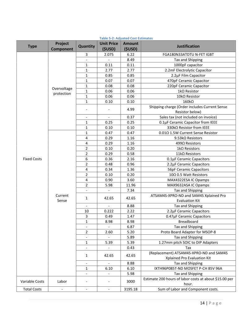
5.4 Adjusted Cost Estimates
Total costs spent on this project differ drastically from initial projections. After adding up all the
fixed costs for component purchases with the variable cost of labor, the project incurred a total cost of
$3,195.18. This difference of about $155 compared to initial costs stems from the fixed costs of the
system. Initial projections did not appropriately consider the cost of a microcontroller, which cost more
than the total initial fixed costs at about $51 after tax and shipping. During the testing phase on the
current sense, the microcontroller stopped working after a poor connection possibly caused the
microcontroller to receive too high of a voltage potential or current and damage the microcontroller.
Replacement ended up costing another $51. Shipping charges represent another factor contributing to
the higher total cost. Each purchase of components from an online source entails an extra charge
ranging from five to nine dollars. in total, the shipping charges alone add to a sum of roughly $62.
Ideally, a single purchase should include all required and necessary components in one order. However,
few online stores carry some specific components like the FGA180N33ATDTU N-FET IGBT (Insulated-gate
bipolar transistor). Table 5-2 tabulates the costs towards the EHFEM’s protection system. The cost table
excludes the 10Ω 300W resistor, Ohmite heatsinks, and the 20V zener diode used in the current sense
circuit because Dr. Braun lent out these items adding no extra cost to the project workers. Although the
costs table lists a 2.2mF capacitor, this capacitor proved insufficient as it has too low of maximum DC
voltage. Conveniently, Dr. Prodanov had a box of 2.5mF capacitors once donated to him, and he
graciously donated a few to the EHFEM projects.
14 | P a g e
Table 5-2: Adjusted Cost Estimates
Type Project
Component Quantity
Unit Price ($USD)
Amount ($USD)
Justification
Fixed Costs
Overvoltage protection
3 2.075 6.22 FGA180N33ATDTU N-FET IGBT
- - 8.49 Tax and Shipping
1 0.11 0.11 1000pF capacitor
1 2.77 2.77 2.2mF Electrolytic Capacitor
1 0.85 0.85 2.2μF Film Capacitor
1 0.07 0.07 470pF Ceramic Capacitor
1 0.08 0.08 220pF Ceramic Capacitor
1 0.06 0.06 1kΩ Resistor
1 0.06 0.06 10kΩ Resistor
1 0.10 0.10 160kΩ
- - 4.99 Shipping charge (Order includes Current Sense
Resistor below)
- - 0.37 Sales tax (not included on invoice)
1 0.25 0.25 0.1μF Ceramic Capacitor from IEEE
1 0.10 0.10 330kΩ Resistor from IEEE
Current Sense
1 0.47 0.47 0.01Ω 1.5W Current Sense Resistor
4 0.29 1.16 9.53kΩ Resistors
4 0.29 1.16 499Ω Resistors
2 0.10 0.20 1kΩ Resistors
2 0.29 0.58 11kΩ Resistors
6 0.36 2.16 0.1μF Ceramic Capacitors
2 0.48 0.96 2.2μF Ceramic Capacitors
4 0.34 1.36 56pF Ceramic Capacitors
2 0.10 0.20 10Ω 0.5 Watt Resistors
4 0.90 3.60 MAX4322ESA IC Opamps
2 5.98 11.96 MAX9632ASA IC Opamps
- - 7.34 Tax and Shipping
1 42.65 42.65 ATSAM4S-XPRO-ND and SAM4S Xplained Pro
Evaluation Kit
- - 8.88 Tax and Shipping
10 0.222 2.22 2.2μF Ceramic Capacitors
3 0.49 1.47 0.47μF Ceramic Capacitors
1 8.98 8.98 Breadboard
- - 6.87 Tax and Shipping
2 2.60 5.20 Proto Board Adapter for MSOP-8
- - 5.89 Tax and Shipping
1 5.39 5.39 1.27mm pitch SOIC to DIP Adapters
- - 0.43 Tax
1 42.65 42.65 (Replacement) ATSAM4S-XPRO-ND and SAM4S
Xplained Pro Evaluation Kit
- - 8.88 Tax and Shipping
1 6.10 6.10 IXTH96P085T-ND MOSFET P-CH 85V 96A
- - 5.98 Tax and Shipping
Variable Costs Labor - - 3000 Estimate 200 hours of labor costs at about $15.00 per
hour.
Total Costs - - - 3195.18 Sum of Labor and Component costs.
15 | P a g e
6 DC-DC Converter Input Protection Circuit
6.1 Input Protection Circuit Design
The input protection circuit must ensure the DC-DC converter’s protection when under normal
user operation of the elliptical and during the startup period for the Enphase Micro-inverter [3]. If a user
exercises with the elliptical for either continuous running or quick sprints, that person generates voltage
transients to the DC-DC convert that exceed its maximum input of 51 V [2]. The startup period for the
Enphase Micro-inverter causes an open load condition for the DC-DC converter, allowing no current to
pass [2]. This requires a means for dissipating excess power as the voltage can build up to unsafe levels.
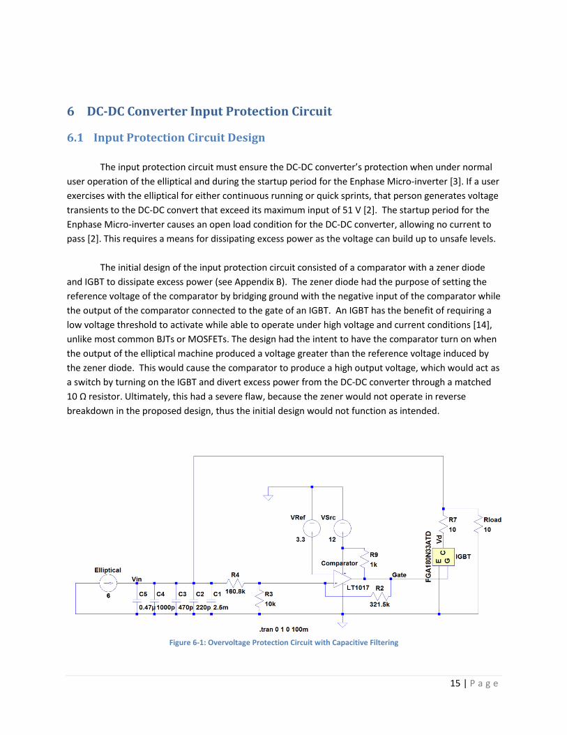
The initial design of the input protection circuit consisted of a comparator with a zener diode
and IGBT to dissipate excess power (see Appendix B). The zener diode had the purpose of setting the
reference voltage of the comparator by bridging ground with the negative input of the comparator while
the output of the comparator connected to the gate of an IGBT. An IGBT has the benefit of requiring a
low voltage threshold to activate while able to operate under high voltage and current conditions [14],
unlike most common BJTs or MOSFETs. The design had the intent to have the comparator turn on when
the output of the elliptical machine produced a voltage greater than the reference voltage induced by
the zener diode. This would cause the comparator to produce a high output voltage, which would act as
a switch by turning on the IGBT and divert excess power from the DC-DC converter through a matched
10 Ω resistor. Ultimately, this had a severe flaw, because the zener would not operate in reverse
breakdown in the proposed design, thus the initial design would not function as intended.
Figure 6-1: Overvoltage Protection Circuit with Capacitive Filtering

16 | P a g e
The newer design seen in Figure 6-1 modifies the initial design by forgoing the zener diode and
establishing a 3.3 V reference voltage from a port of the microcontroller used for the current limiter. A
voltage divider scales down the output voltage generate from the elliptical machine so that the
comparator can output high when the positive input terminal exceeds 3.3 V. The comparator utilizes a
feedback resistor for hysteresis and a pull-up/pull-down resistor that bridges the output of the
comparator to the elliptical's on-board 12 V battery. The output of the comparator still connects to the
gate of the IGBT. The hysteresis allows the comparator to activate the IGBT at a voltage level just below
the maximum input of 60 V and divert excess power until it reaches a lower voltage level to turn off the
comparator and IGBT.
The IGBT selected has a high collector to emitter voltage, collector current, and power
dissipation ratings as well as a low saturation voltage [14]. These allow the IGBT to withstand power
dissipating up to 156 W at 100°C, more than enough when used in application with the elliptical
machine.
This design also utilizes the capacitive filtering designed by Ryan Turner and Zack Weiler from
their DC-DC Converter Input Protection System design [2]. The capacitive filtering combines filtering and
decoupling capacitors to filter out high frequency transient responses induced by the elliptical when in
use. The 2.5 mF filter capacitor flattens large fluctuations in the waveform down to an average value of
the signal [2] while the other decoupling capacitors filter out high frequency transients that exceed
limitations of the DC-DC converter at the input. Figure 6-2 and 6-3 depict simulations of the designed
input protection system.
Figure 6-2: Vin & Vgate simulation

17 | P a g e
Figure 6-3: Power Dissipation of the 10 Ω diverting resistor (R7) (Blue) and IGBT (Green)
The simulation shown in Figure 6-2 illustrates the comparator's operation in conjunction with
the IGBT. When the input voltage reaches 58 V, the comparator pulls high to 12 V, thus turning on the
IGBT to divert excess current through a 10 Ω resistor. Again, the feedback resistor provides hysteresis.
as the IGBT diverts excess power, the voltage at Vin declines over an interval less than 3 ms, until it
reaches a voltage level of 52 V. Once the voltage drops below that level, the comparator’s output pulls
low and this in turn turns off the IGBT. Figure 6-3 details the power dissipation of the overvoltage
protection design. When the IGBT turns on and diverts the excess power going into the DC-DC
converter, the diverting resistor R7 and load resister Rload experience a summed maximum power
dissipation of 330 W. This emphasizes the need for a diverting resistor capable of handling such a large
dissipation of power.
Meanwhile, the power dissipated through the gate and collector sum to a maximum power
dissipation of about 85 W as the IGBT turns on before quickly leveling to 5 W. The IGBT selected for the
overvoltage protection design has a maximum power dissipation of 390 W at room temperature [14].
6.2 Testing the Input Protection Circuit
Preliminary testing seeks to prove whether the designed prototype would operate in
accordance to the simulations. Before testing with the elliptical machine, the input protection circuit
must prove capable of voltages above the specified limits via DC source. The circuit must undergo low
power testing before testing with high power. to accomplish this, 51 kΩ resistors take the place of the
10 Ω resistors to limit the current and power dissipated through the circuit. Preliminary testing utilizes
the schematic in Figure 5-1. Figure 6-5 below shows a Fritzing diagram of the breadboard layout and
labels for wire connections.

18 | P a g e
Testing Specifications
The over voltage protection circuit must divert power through the IGBT when the voltage at
node Vin rises to 58 V.
The IGBT should turn off when the voltage at Vin drops below 52 V.
Test Equipment
Prototype of overvoltage protection circuit constructed on a breadboard
DC voltage source capable of supplying up to 150 V
DC voltage supply of 12 V
Kiethley source meter
51 kΩ resistors in place of 10 Ω resistors
Oscilloscope
2 Scope probes
banana-to-grabber cables
Figure 6-4: Low Current Test Circuit

19 | P a g e
Figure 6-5: Breadboard Diagram of Overprotection Circuit Layout for Low Power Testing
Preliminary testing of the circuit does not require all components of the final design. When
testing with a DC source, the capacitive filtering excludes the 2.5 mF capacitor. Testing with the
capacitor now could prove more hazardous than beneficial as a charged 2.5 mF capacitor can harm a
tester. Once testing with the elliptical machine occurs, then testing requires the capacitor as it helps
smooth any high frequency transient responses to an average DC value when using the elliptical. Also, a
voltage divider from the 12 V DC source has to compensate for the lack of a 3.3 V source from the
absent microcontroller.
A couple issues arose, which hindered testing. The comparator could not activate the IGBT when
the input had a high enough voltage, because the positive input of the comparator bridged to ground
instead of the 12 V rail. Another issue that hindered progress was the ground terminal of the Kiethley
source meter probing the positive rail of the breadboard instead of the ground rail on the board.
Ultimately, testing the prototype of the overvoltage protection circuit proved successful but not
quite as expected. The voltage divider used in testing scaled down the 12 V supply to 3.8 V instead of
the desired 3.3 V. This caused the comparator output to go high and activate the IGBT when the input
reached 70 V instead of the desired 60 V. Likewise, the IGBT turned off when the input voltage dropped
down to a level of 60 V. While the circuit did not test in accordance to the above simulations, this
preliminary testing still provides a successful operation of the circuit.

20 | P a g e
6.3 High Power Testing
In order to test the overvoltage protection circuit under high power conditions, the circuit below
utilizes a high power source and an electronic load. for this test session, the IGBT should divert excess
power when the input at Vin in Figure 6-5 charges to 51 V. An input voltage of 51 V allows the positive
terminal of the comparator to exceed its negative terminal and output a high voltage of 12 V to node
“Gate” thus turning on the IGBT. The comparator with hysteresis resistor allows for the comparator’s
positive terminal to maintain a voltage greater than the negative terminal allowing until the voltage
level of Vin lowers to 45 V. without the hysteresis, the comparator and IGBT turn off when Vin falls below
51 V, which would cause continuous switching due to a constant fluctuating voltage level. After diverting
power, the comparator turns off the IGBT once the input voltage lowers to 45 V.
Test Equipment
● Agilent E3630A Triple Output DC Power Supply (12 V)
● BK Precision 9153 60V/9A 540W Programmable DC High Power Supply
● Agilent MSO-X 2012A mixed Signal Oscilloscope
● Agilent U3606A Multimeter
● Agilent E33220A Function Generator (if not using 3.3 V source from microprocessor)
● BK Precision 8514 1200W Programmable DC Electronic Load (if not using two 10 Ω resistors)
● Two 10 Ω resistors rated for 300 Watts
● Atmel SAM4S Xplained Pro Microprocessor
● Overvoltage protection circuit
● Heatsink for IGBT
● 1 BNC-grabber
● 6 Banana-Grabber
● 6 Banana-Banana
● 4 spade-banana cables
● 10 alligator clips

21 | P a g e
Figure 6-6: LT Spice Protection Circuit Schematic
Figure 6-6 depicts the LT Spice schematic used for the simulated results seen in Figure 6-6. The
Schematic uses different resistor values for the voltage divider and hysteresis. Since testing the
overvoltage protection circuit under lower power conditions, Byung Yoo and Sheldon Chu, changed
their required input voltage value to their DC-DC converter. This requires the overvoltage protection
circuit to divert excess power through a matched 10 Ω at a voltage level lower than the previously
defined specification of 60 V to 51 V. Figure 6-7 below shows the updated simulation and figure 6-8
depicts an accurate breadboard representation of the testing protection circuit with labels for testing
equipment.
Figure 6-7: Vin and Vgate for Updated 51 Volt Specifications
Including the 2.5 mF Capacitor remains only necessary when testing with the elliptical machine
since it filters out high frequency transient responses from the elliptical [2]. as with low power testing,

22 | P a g e
testing with the capacitor now could prove more hazardous than beneficial as a charged 2.5 mF
capacitor can harm a tester. All capacitors used in this circuit must have a high maximum voltage rating
so that they do not burn out when undergoing high power testing [2].
Figure 6-8: Breadboard Layout of Overvoltage Protection Circuit
Note: Depicted 10 Ω resistor in Figure 6-8 cannot dissipate the required 360 W.
Test Case:
Starting at 40 V, increase the voltage of the high power supply to 53 V and fill out the data table
in Table 6-1 below. Make note of the voltage that activates the comparator and IGBT. Following that,
decrease the input voltage to 45 V, and continue to fill out the data table. Again, note the voltage when
the comparator deactivates and turns off the IGBT.
Expected Result:
Comparator should output high (12V) once Vin reaches 51 volts. Comparator should output low
(~0V) once Vin goes back down to 45.5V.

23 | P a g e
Table 6-1: Tabulated Data for High Power Testing
Startup - Input voltage increases; IGBT starts OFF
Vin V+ (V) VGate (V)
Vc of IGBT (V)
R7 (Ω)
Rload (Ω)
Vsupply measured (V)
Isupply (A)
Dissipated Power (W) IR7 (A)
IRload (A)
40 2.560 0.01 39.4 10.2 10 39.999 3.956 158.236 0 3.955
50 3.250 0.12 49.2 10.2 10 49.997 4.945 247.2352 0 4.944
50.5 3.283 0.11 50.1 10.2 10 50.497 4.994 252.182 0 4.993
50.7 3.2965 0.12 50.3 10.2 10 50.696 5.014 254.1897 0 5.013
51 3.370 11.95 0.77 10.2 10 46.843 9.097 426.1308 4.548 4.548
52 3.3725 11.95 0.793 10.2 10 46.820 9.097 425.9215 4.548 4.548
53 3.3695 11.95 0.793 10.2 10 46.793 9.097 425.6759 4.548 4.548
Decrease input voltage; IGBT starts ON
53 3.370 11.95 0.77 10.2 10 46.76 9.097 425.3757 4.548 4.548
52 3.378 11.95 0.781 10.2 10 46.79 9.097 425.6486 4.548 4.548
51 3.380 11.95 0.773 10.2 10 46.83 9.097 426.0125 4.548 4.548
50 3.385 11.95 0.770 10.2 10 46.89 9.097 426.5583 4.548 4.548
49 3.391 11.95 0.771 10.2 10 46.96 9.097 427.1951 4.548 4.548
48.5 3.392 11.95 0.769 10.2 10 46.98 9.097 427.3771 4.548 4.548
48 3.394 11.95 0.767 10.2 10 46.99 9.097 427.468 4.548 4.548
47 3.394 11.95 0.765 10.2 10 46.99 9.073 426.3403 4.546 4.546
46.5 3.361 11.95 0.764 10.2 10 46.49 8.975 417.2478 4.397 4.397
46 3.329 11.95 0.763 10.2 10 45.99 8.876 408.2072 4.437 4.437
45.5 3.295 7.71* 10.21 10.2 10 44.49 8.776 390.4442 4.443 4.443
45 2.925 0.11 44.60 10.2 10 44.49 4.449 197.936 0 4.448 *The voltage level of the gate slowly but continued to decline from the initial reading of 7.71 volts.
IGBT switched on when Vin = 50.75 V and switched OFF when Vin = 45 V.
Initial testing used the 3.3 V source from the Atmel microcontroller. When used, power diverted
through the IGBT when Vin reached 50.3 V because the voltage source from the microcontroller
measured 3.26 V with a multimeter. This allows for power to divert from the DC-DC converter at a lower
voltage level than expected and further prevents the DC-DC converter from damage. When further
testing took place, an Agilent function generator took the place of the absent Atmel for the 3.3 V source.
Consequently, power diverted through the IGBT when Vin reached a slightly higher level of 50.75 V.
Initial testing also included a BK Precision electronic load set to 10 Ω. Testing discovered that the
electronic load has a maximum voltage limit of 38 V, which lead to testing difficulties and inaccurate
data measurements so a 10 Ω load took its place. Table 6-1 above reflects data taken when testing with
the Agilent outputting a 3.3 V DC source and a 10 Ω load in place of the electronic load.
When lowering the voltage from 53 V, power dissipates through the IGBT and matched 10 Ω
resistor until Vin lowers to 45 V. Table 6-1 shows that when Vin lowers to 45.5 V, the hysteresis causes

24 | P a g e
the voltage level of V+ to equal 3.2957 V, a voltage lower than the source supplied by the function
generator. This shows a transition period from the IGBT switching from an on to OFF state as evident of
the VGate lowering to 7.7 V and declining. Meanwhile the current supplied by the BK Precision high power
supply still outputs a current double than it would normally with a deactivated IGBT of 8.776 A.
Note that when V+ surpasses the 3.3 V source at the negative comparator terminal and the
comparator outputs a high voltage to the gate of the IGBT, the BK Precision power supply reaches its
output current limit of 9.1 A. The voltage supplied by the DC high power supply drops to 46.78 V so that
the power source does not surpass its current limit. Before power dissipates through the IGBT and a
matched 10 Ω resistor, the power source supplies a current close to 5 A. This total current would have
jumped to about 10 A had the DC high power supply not have a limit. Should the DC high power supply
have the capability to output 10 A at 51 V, the circuit would dissipate a total of about 510 W. Since the
current splits between the two 10 Ω resistors, each resistor would dissipate a maximum of about 255 W,
well below the maximum power dissipation for the resistors.
Testing shows that the IGBT activates and diverts excess power at an input voltage 0.25 V lower
than the expected 51 V and deactivates 0.5 V lower than the anticipated 45.5 V. Through high power
testing, the overvoltage protection circuit proves it can handle high current conditions and function as
expected.
7 Current Limiter/Diverter Circuit
7.1 Current Limiter/Diverter Design
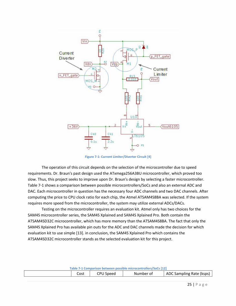
The design for the current limiter/diverter circuit uses the design from Dr. Braun's Sabbatical
Report [4]. Figure 7-1 shows the schematic with the current diverter and current limiter labeled. The
circuit has the objective of limiting the current between the DC-DC converter and the inverter to 6.4 A
[4]. This occurs through the use of two transistors: an IGBT to divert extra power and a PMOS to limit
the current. The PMOS requires the use of a zener diode with a reverse breakdown voltage of 20 V
because it has a maximum VGS of 25 V [15]. The figure excludes the microcontroller that drives the gates
of both transistors through the use of two DAC channels. The microcontroller takes in ADC inputs from
four nodes in the circuit (Vin, Vdn, Vdp, and Vout6105) to calculate what voltages to output from the DACs.
25 | P a g e
Figure 7-1: Current Limiter/Diverter Circuit [4]
The operation of this circuit depends on the selection of the microcontroller due to speed
requirements. Dr. Braun's past design used the ATxmega256A3BU microcontroller, which proved too
slow. Thus, this project seeks to improve upon Dr. Braun's design by selecting a faster microcontroller.
Table 7-1 shows a comparison between possible microcontrollers/SoCs and also an external ADC and
DAC. Each microcontroller in question has the necessary four ADC channels and two DAC channels. After
computing the price to CPU clock ratio for each chip, the Atmel ATSAM4S8BA was selected. If the system
requires more speed from the microcontroller, the system may utilize external ADCs/DACs.
Testing on the microcontroller requires an evaluation kit. Atmel only has two choices for the
SAM4S microcontroller series, the SAM4S Xplained and SAM4S Xplained Pro. Both contain the
ATSAM4SD32C microcontroller, which has more memory than the ATSAM4S8BA. The fact that only the
SAM4S Xplained Pro has available pin outs for the ADC and DAC channels made the decision for which
evaluation kit to use simple [13]. in conclusion, the SAM4S Xplained Pro which contains the
ATSAM4SD32C microcontroller stands as the selected evaluation kit for this project.
Table 7-1 Comparison between possible microcontrollers/SoCs [12]
Cost CPU Speed Number of ADC Sampling Rate (ksps)

26 | P a g e
(MHz) Integrated ADCs|DACs
Atmel 32-bit A3 Series 18.37 84 8 | 2 384
Atmel 32-bit C Series 16.02 66 16 | 4 2000
Atmel 32-bit A0 Series 15.48 66 8 | 2 384
Atmel xMega A3 Series 7.46 32 4 | 2 2000
Xilinx XC7Z020-1CLG400C
108.20 667 NA NA
Atmel ATSAM3S2BA 5.24 64 10 | 2 1000
Atmel ATSAM3U2CA 6.10 96 4 | 4 1000
Atmel ATSAM4S8BA 7.70 120 11 | 2 1000
Atmel ATSAM3A4CA 9.02 84 16 | 2 1000
Atmel ATSAM3X4CA 10.17 84 16 | 2 1000
Atmel ATSAM4E8CA 9.42 120 16 | 2 1000
MAX11060GUU 6.48 NA 4 | 0 3000
MCP4922T-E/SLTR 1.99 NA 0 | 2 NA
Figure 7-2 depicts the Xplained Pro evaluation board with important features labeled. Features
important to this project include: ADC pin outs (pins 3:4 on extension header 1 and pins 3:4 on
extension header 2), DAC pin outs (pins 10:11 on spare signals), 3.3 V voltage source (pin 3 on Power
Header), AREF measurement, and AREF adjustment. The AREF provides the reference voltage for the
ADC and the DAC adjusted to 3.3 V.

27 | P a g e
Figure 7-2: SAM4S Xplained Pro Evaluation Kit (ATSAM4SD32C Microcontroller) [13]
The current limiter circuit in Figure 7-1 requires operational amplifiers to bridge the connections
between the circuit itself and the microcontroller pins. Figure 7-3 depicts the non-inverting op-amps
that amplify the voltage output from the two DAC channels on the microcontroller [4]. Both have a gain
of 12 in order to drive the transistor gates at full range.

28 | P a g e
Figure 7-3: Non-Inverting Amplifiers for DAC Outputs (Gain = 12) [4]
Figure 7-4 depicts a voltage follower along with a voltage divider for each ADC connection. The voltage
divider cuts the voltage down to 5% of the respective node voltage in order to drop within the range of
the ADC (0 to 3.3 V).

29 | P a g e
Figure 7-4: Voltage Followers and Voltage Dividers for ADC Inputs [4]

30 | P a g e
7.2 Testing the Current Limiter
Testing began with ensuring each of the individual components functioned properly. Printing
out ADC values from the four channels using a terminal program called Tera Term allowed for testing
the ADC. A multimeter then compared a voltage reading with the ADC values at the respective circuit
nodes. Similarly, DAC values compared with voltage readings at the gates of each transistor. Transistor
testing entailed ensuring the transistors switched on and off at acceptable voltages according to their
datasheets. The current sense amplifier, the last component tested, ideally functioned by outputting a
voltage directly related to the current flowing through a connected sense resistor [4]. However, after
numerous attempts to obtain acceptable output voltages from the current sense amplifier, it became
clear that the amplifier had become inoperable and thus could not provide accurate current readings.
Failure to operate may have resulted from electrostatic discharge due to poor handling or through
overheating during the soldering process. The node between the drain of the PMOS and a 10.3 Ω
resistive load became the new node for the current sense ADC reading as a temporary fix in order to
continue testing.
A written test program required the use of Dr. Braun's prior test program as a foundation [4].
The program, located in Appendix B, utilizes the Atmel Software Framework (ASF) to provide necessary
functionality for key components such as the ADC and DAC. Running the program relies on access to a
serial terminal such as Tera Term. on startup, the user may enter a command to run a specific operation.
User Commands
'p' Print out the 4 ADC values and 2 DAC values
'w' Increase n_FET_gate DAC value by 1
'W' Increase n_FET_gate DAC value by 10
's' Decrease n_FET_gate DAC value by 1
'S' Decrease n_FET_gate DAC value by 10
'e' Increase p_FET_gate DAC value by 1
'E' Increase p_FET_gate DAC value by 10
'd' Decrease p_FET_gate DAC value by 1
'D' Decrease p_FET_gate DAC value by 10
'1' Test p_FET_gate
'2' Test n_FET_gate
'r' Run the current limiting test program
The current limiting test program works by reading in the voltage from the current sense
amplifier and changing the p_FET_gate and n_FET_gate voltages based off the read in voltage. for
example, if the read in voltage has a higher voltage than the goal voltage, the p_FET_gate voltage may
increase to turn off the PMOS. The n_FET_gate voltage may also increase to turn on the IGBT.
Test Equipment

31 | P a g e
● BK Precision 9153 60V/9A 540W Programmable DC High Power Supply (20 V)
● Two 10 Ω resistors rated for 300 Watts
● Agilent E3630A Triple Output DC Power Supply (24V)
● Agilent MSO-X 2012A mixed Signal Oscilloscope
● Agilent U3606A Multimeter
● Atmel SAM4S Xplained Pro Microprocessor
● Current limiting circuit
● 4 banana-grabber
● 2 spade-banana
● 4 banana-banana
● 1 Scope Probe
● Heatsink for IGBT and PMOS
● 8 alligator clips
● Laptop running Tera Term and Atmel Studio 6.1
● Microcontroller code (Appendix B)
Figure 7-5: Breadboard Layout of Current Limiter Circuit (Not to Scale)
Figure 7-6 shows the ADC values for the circuit with and without the current sense amplifier. Vin,
Vdn, Vdp, and Vout/Vout6105 represent the four ADC values. with ADC values close to 20 symbolizing 0 V, it
remains clear that the current sense amplifier outputs close to 0 V even with 20 V at the input. The rest
of the testing excludes the current sense amplifier. The MAX4322 and MAX9632 chips lay on 1.27mm
pitch SOIC to DIP Adapters allowing for testing with a breadboard. These adapters cover more of the breadboard

32 | P a g e
vertically than depicted in Figure 7-6 appearing that the decoupling capacitors lay too far from the chip. The non-
ground pins of decoupling capacitors must lie within one-tenth of an inch of the pin on interest to reliably filter out
voltage spikes that may damage the integrated circuit.
NOTE: The following tests had Vin set to 20 V.
ADC values shown in Figure 7-7 demonstrate the gate voltage values required to change each of
the transistor's state. in particular, the IGBT turns on at voltages above 6.85 V and the PMOS turns off at
voltages above 18.4 V provided that Vin is set to 20 V. These values match well the expected values from
the transistor datasheets [14-15]. in Figure 7-7 the first DAC value corresponds with the IGBT gate and
the second corresponds with the PMOS gate.
Figure 7-6: ADC Values with and without the Current Sense Amplifier
Figure 7-7: ADC Values/DAC values for Different Transistor States

33 | P a g e
Table 7-2 shows each of the test runs performed with different Vgoal values set for each test case
ranging from numerical 600 to 1200. The voltage at Vout fluctuated due to the microprocessor program
trying to control the gate voltages. Each case proves successful in that the output at Vout limits to a value
closely to the set Vgoal value in the program. Due to testing equipment limitations (i.e. lack of two 36 V
power supplies) higher current testing could not occur. This prevented testing of the target current
value from the supply of 6.1 A.
Table 7-2 Current Limiting Data
Vin
(V) Isupply (A) Vgoal
(ADC) Vgoal (V) Vout Min
(V) Vout Max
(V) Vout Avg
(V) Iout Avg
(A) Power
Dissipated (W)
20 2.804 600 9.73 8.6 8.8 8.7 0.84 56.08
20 3 700 11.35 9.6 11.1 10.35 1.00 60
20 3.3 800 12.97 13.6 14.3 13.95 1.35 66
20 3.42 900 14.59 14.6 15.8 15.2 1.48 68.4
20 3.6 1000 16.21 15.9 17 16.45 1.60 72
20 3.56 1100 17.84 14.4 16.4 15.4 1.50 71.2
20 1.955 1200 19.46 19.4 19.5 19.45 1.89 39.1
7.3 Current Limiter Timing
In order for the current limiter to succeed, the microcontroller controlling the transistor gate
voltages must have enough speed to keep up with the changing current flowing from the input to the
output of the circuit. The first measurement of speed capabilities came from the real time timer (RTT) in
the microcontroller. on average, it takes about 4.2 μs (238 kHz) to read four ADC channels and output to
two DAC channels.
For timing considerations during actual testing, one problem came up that the authors of this
report could not fix. In order for the current limiting while() loop to function correctly, the program
requires a printf() statement inserted into the loop. Without the printf() statement, nothing writes from
the DACs even though the program still runs. However, having the printf() there slows down the
program considerably.
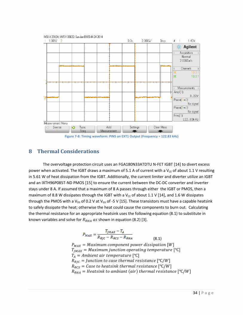
To measure the speed, PIN5 on EXT1 toggled high and low each iteration through the while()
loop. Figure 7-9 shows the waveform from PIN5 along with the frequency of 122.83 kHz. This frequency
value must double to obtain the true frequency of the loop since it takes two iterations to complete a
cycle in the waveform thus providing a frequency of 245.66 kHz.
34 | P a g e
Figure 7-8: Timing waveform: PIN5 on EXT1 Output (Frequency = 122.83 kHz)
8 Thermal Considerations
The overvoltage protection circuit uses an FGA180N33ATDTU N-FET IGBT [14] to divert excess
power when activated. The IGBT draws a maximum of 5.1 A of current with a VCE of about 1.1 V resulting
in 5.61 W of heat dissipation from the IGBT. Additionally, the current limiter and diverter utilize an IGBT
and an IXTH96P085T-ND PMOS [15] to ensure the current between the DC-DC converter and inverter
stays under 8 A. If assumed that a maximum of 8 A passes through either the IGBT or PMOS, then a
maximum of 8.8 W dissipates through the IGBT with a VCE of about 1.1 V [14], and 1.6 W dissipates
through the PMOS with a VDS of 0.2 V at VGS of -5 V [15]. These transistors must have a capable heatsink
to safely dissipate the heat; otherwise the heat could cause the components to burn out. Calculating
the thermal resistance for an appropriate heatsink uses the following equation (8.1) to substitute in
known variables and solve for shown in equation (8.2) [3].
(8.1)
( )

35 | P a g e
(8.2)
Looking at the datasheet for the IGBT, the maximum junction operating temperature, ,
equals 100 , and the junction to case thermal resistance, , equals 0.32 [20]. Meanwhile the
maximum component power dissipation, , equals 5.61 W for one IGBT and 8.8 W for the other. The
datasheet for the PMOS reveals that it’s equals 125 , its equals 0.42 [20] and
dissipates an estimate power of 1.6 W. for both, assume an ambient air temperature of 25 , and
assume a case to heatsink thermal resistance, , of 0.15 [3].
(8.3)
(8.4)
( )
⁄ (8.5)
The calculations given by (8.3), (8.4), and (8.5) yields the maximum allowed heatsink to ambient thermal
resistance as 8.05 . While the two IGBTs and PMOS may utilize separate brands of heatsinks, for
simplicity the three used in this project use the same kind of heatsink. to comply, this heatsink must
have a thermal resistance less than 8.05 . Shown in Figure 9 below, the MA-302-55E heatsink
suffices excellently for heat dissipation with a thermal resistance of 3 in still air [3], less than half
that of the calculated maximum value.
Figure 8-1: MA-302-55E Heatsink [20]

36 | P a g e
9 Conclusion and Future Projects
The previously designed input protection system developed by Zack Weiler and Ryan Turner
proved successful [2] in protecting Martin Kou’s DC-DC Converter for maximum specifications of 65 V
and 6.5 A [3]. The current sense circuit Zack and Ryan designed functioned to divert current to ground
when the inverter enter a start-up phase and allow current flow back to the inverter when a current
sense resistor detects current flow [2]. While this design succeeded in protecting under all modes of
operation, the circuit demonstrated poor efficiency due the circuit dissipating all generated power while
diverting current from the inverter. This project aimed to develop a new input protection system with an
improved overall efficiency while adhering to the specifications of a DC-DC converter concurrently
developed by students Byung Yoo and Sheldon Chu [7].
Chapters 6 and 7 detail the final design of the two-part system developed by the two authors of
this paper. This first part consists of an overvoltage protection circuit to limit the input to the DC-DC
converter to a maximum of 51 V and 5.1 A [7]. This circuit utilizes the same high efficiency capacitive
filtering/decoupling developed by Zack and Ryan in their design to average the high frequency transient
responses from the elliptical machine into a smooth DC value [2]. The overvoltage protection design in
this paper includes a voltage divider and comparator to activate an IGBT to divert excess power. The
resistors in the voltage divider can easily change should the DC-DC converter require an increase or
decrease in its maximum input voltage. Because of this, the overvoltage protection circuit can adapt to
almost any DC-DC converter and not require the modification of a DC-DC converter’s characteristics. The
implementation of the comparator allows the input protection circuit to divert excess power even
during the Enphase Micro-inverter’s five minute start-up period [2]. So long as the IGBT diverts excess
power through a matched 10 Ω load, an input voltage cannot build up to dangerous levels due to the
elliptical. Unfortunately, the prototype resides on a breadboard at the time of this report. Should future
projects attempt to improve upon the design proposed in this paper, the overvoltage protection circuit
should transfer to a PCB for elliptical testing. Including banana plugs on the PCB design allow for easy
compatibility with testing equipment.
The second part of the DC-DC converter protection circuit limits the current between the DC-DC
converter and the inverter to 6.4 A [7]. The proposed design utilizes a current sense resistor of 0.010 Ω
with a high current sense amplifier and PMOS to limit the current between the DC-DC converter and
inverter. An N-FET IGBT and 10 Ω resistor bridge the output of the DC-DC convert and ground to divert
any excess current. While the inverter can handle a maximum current of 8 A, the design in this paper
limits the current to only deliver as much power as the inverter can convert [4]. A microcontroller
regulates the switching of the IGBT and PMOS by reading the voltage values at important nodes in the
circuit (Vin, Vdn, Vdp, and Vout6105 as described in Chapter 7.1). The microcontroller takes in ADC inputs
from four nodes to calculate what voltages to output from the DACs, which connect to the gates of the
IGBT and PMOS via a non-inverting amplifier. Unfortunately, the high current sense amplifier failed to
work during testing phases of the current sense circuit. Electrostatic discharge from poor handling or
overheating while soldering may have cause the amplifier to fail. While testing continued with a

37 | P a g e
temporary fix, future projects would greatly improve the design by having a fully-operational high
current sense amplifier. as with the overvoltage protection circuit, the circuit for the current sense exists
on a breadboard, and should eventually adapt to a PCB layout.
As previously, stated the authors of this report recommend converting the designs for the
existing or improved upon prototypes to a printed circuit board. The prototype for the current sense
lacks a functioning high current sense amplifier and implementing one that functions ideally would make
for a great improvement. Zack and Ryan allude to designing an inverter specifically for the EHFEM
project as another possible improvement in their report [2]. A customized inverter for the EHFEM
project could improve the overall efficiency of the project while having a reduced start-up period
compared to the Enphase Micro-inverter.
Even though the current sense circuit experienced setbacks, the circuit still functions as a means
of regulating current. that aside, the overvoltage protection designed in this paper proposes an effective
method at regulating the input voltage and diverting excess power to the DC-DC converter.

38 | P a g e
References
[1] D. Braun. "Braun's Senior Projects," Cal. Poly. State Univ. EE Dep., 12 June 2012. [Online]. Available:
http://courseware.ee.calpoly.edu/~dbraun/srproj.htm. [Accessed 20 November 2012].
[2] R. Turner and Z. Weiler. DC-DC Converter Input Protection System for the Energy Harvesting from Exercise Machines (EHFEM) Project. San Luis Obispo: Cal Poly State Univ., Electrical Engineering Dep., June 2013. [Online]. Available: http://digitalcommons.calpoly.edu/cgi/viewcontent.cgi?article=1226&context=eesp. [Accessed 23 Dec 2013].
[3] M. Kou. Energy Harvesting from Elliptical Machines: DC-DC Converter Design Using SEPIC Topology. San Luis Obispo: Cal Poly State Univ., Electrical Engineering, M.S. Thesis, 2012. Available: http://digitalcommons.calpoly.edu/cgi/viewcontent.cgi?article=1797&context=theses [Accessed 23 Dec 2013]
[4] D. Braun. “Post-Leave Report for Spring 2012 Sabbatical,” San Luis Obispo: Cal Poly State Univ., Electrical Engineering. 15 Oct 2012.
[5] M. Lum and J. Yuen. Energy Harvesting from Elliptical Machines. San Luis Obispo: Cal Poly State Univ., Electrical Engineering Dep., Dec 2009. [Online]. Available: http://digitalcommons.calpoly.edu/cgi/viewcontent.cgi?article=1015&context=eesp. [Accessed 23 Dec 2013].
[6] E. Cannella and F. Marino. “DC-DC Converter with Current Overload Protection Circuit and Method.” Stmicroelectronics S.R.L., assignee. Patent US7940030 B2. 29 July 2008. [Online]. Available: http://www.google.com/patents/US7940030. [Accessed: 26 Dec 2013].
[7] B. Yoo and S. Chu. BUCK-BOOST DC-DC CONVERTER with INPUT PROTECTION SYSTEM for THE ENERGY HARVESTING from EXERCISE MACHINES PROJECT. San Luis Obispo: Cal Poly State Univ., Electrical Engineering Dep., June 2014.
[8] Franco, Sergio. Design with Operational Amplifiers and Analog Integrated Circuits. 3rd ed. New York: McGraw-Hill, 2002. Print.
[9] Enphase Energy, "Installation and Operations Manual M175-24-240-S," 16 Jun 2008. [Online].
Available: http://enphase.com/downloads/8168M175-24-240-SUserManualV14.pdf. [Accessed 29 Dec 2013].
[10] Littlefuse, "Transient Suppression Devices and Principles," Jan 1998. [Online]. Available: http://www.littelfuse.com/data/en/Application_Notes/an9768.pdf. [Accessed 29 Dec 2013].
[11] Texas Instruments, "Filtering Techniques: Isolating Analog and Digital Power," October 2001. [Online]. Available: http://www.ti.com/lit/an/scaa048/scaa048.pdf. [Accessed 29 Dec 2013].
[12] Atmel, "ARM-based Flash MCU SAM4S Series Datasheet," January 2014. [Online]. Available: http://www.atmel.com/Images/Atmel_11100_32-bit-Cortex-M4-Microcontroller_SAM4S_Datasheet.pdf. [Accessed 28 Jan 2014].
[13] Atmel, "User Guide SAM4S Xplained Pro," March 2013. [Online]. Available: http://www.atmel.com/images/atmel-42075-sam4s-xplained-pro_user-guide.pdf. [Accessed 28 Jan 2014].
[14] Fairchild Semiconductor, "FGA180N33ATD 330 V PDP Trench IGBT," October 2013. [Online]. Available: https://www.fairchildsemi.com/ds/FG/FGA180N33ATD.pdf. [Accessed 15 Feb 2014].
[15] IXYS, "TrenchP Power MOSFETs," 2013. [Online]. Available:
http://ixapps.ixys.com/DataSheet/DS100025B(IXTA-TH-TP96P085T).pdf. [Accessed 7 June 2014].

39 | P a g e
[16] Linear Technology, "LT6101/LT6101HV High Voltage, High-Side Current Sense Amplifier in SOT-23." 2006. [Online]. Available: http://cds.linear.com/docs/en/datasheet/6101fh.pdf. [Accessed 29 Dec 2013].
[17] Linear Technology, "Precision, Extended Input Range Current Sense Amplifier," [Online]. Available:
http://cds.linear.com/docs/en/datasheet/6105fa.pdf. [Accessed 7 June 2014].
[18] Maxim Integrated, "Wide-Band Amplifier," 2011. [Online]. Available:
http://datasheets.maximintegrated.com/en/ds/MAX9632.pdf. [Accessed 7 June 2014].
[19] Maxim Integrated, "Rail-to-Rail I/O Op Amps," 2002. [Online]. Available:
http://datasheets.maximintegrated.com/en/ds/MAX4322-MAX4329.pdf. [Accessed 7 June 2014.
[20] Ohmite, "M Series Heatsinks," [Online]. Available: http://www.ohmite.com/cat/sink_m.pdf.
[Accessed 10 June 2014].

40 | P a g e
Appendix A — Project Analysis
Project Title: Protection System for Energy Harvesting from Exercise Machines
Student Names: Eric Funsten and Cameron Kiddoo
Advisor’s Name: David Braun
Summary of Functional Requirements
The DC-DC converter must operate within set input voltage and current parameters. Concurrent
with this project, students Byung Yoo and Sheldon Chu have developed a new DC-DC converter design
with an operational range of 6 V to 51 V [7]. This paper proposes a design for an overvoltage protection
circuit to limit the input of Yoo’s and Chu’s DC-DC converter to within its operational range. The input
protection circuit regulates the incoming voltage from the elliptical machine and filters out any high
frequency transient responses with capacitive filtering to generate a smooth DC signal. The circuit also
functions to divert excess voltage and current that accumulates during the Enphase Micro-invert’s
startup period where an open load appears across the DC-DC converter leading to an overvoltage level
[3]. The report lists the complete specifications for this project in Chapter 3.
Primary Constraints
The input protection must regulate the incoming voltage from the elliptical machine and filter
out any high frequency transient responses with capacitive filtering to generate a smooth DC signal. The
circuit must also divert excess voltage and current that accumulates during the Enphase Micro-inverter’s
startup period where an open load appears across the DC-DC converter [3]. The inverter has a limit to
how much power it can convert from a given current output from the DC-DC converter. Because the
inverter may overload the DC-Dc converter, a current limiter must regulate the current between the two
circuits [4]. This project must provide the necessary protection for the DC-DC converter while still
allowing for maximum power draw efficiency. in order for the EHFEM project to become a viable system
in the future, the benefits must outweigh the costs and this protection system project seeks to move the
EHFEM project one step further.
Economics Economic Impact:
Human Capital – The final implementation of the system required skilled laborers for installing
the input protection system onto an elliptical. The system may require additional technicians to
maintain the electronic components throughout the system's lifespan.
Financial Capital – Components purchased from available vendors and the skilled laborers
involved with the final production require compensation through financial capital. The final
implementation of the EHFEM project aims to have the benefits from generated electricity to
outweigh the costs of the project.

41 | P a g e
Manufactured or Real Capital – The protection system contains several electrical components
including a microcontroller, resistors, capacitors, amplifiers, transistors, a zener diode, and a
comparator.
Natural Capital – Individual components use up natural resources which include: copper, silicon,
and ceramic material. The EHFEM project enables the generation of renewable energy for the
Recreational Center.
Accumulation of Costs and Benefits:
Most of the costs stem entirely up front in the production of the system. Additional costs may
accumulate due to the need to maintain the system for several years. The generated electricity
provides the benefits to the system which must outweigh the costs in less than the given time
frame of 10 years in order for to consider this a viable project.
Project Costs:
Costs associated with this project stem from components purchased for designing and testing
purposes and used in the final design. Table A-1 breaks down the initial costs estimates for these
components as well as estimated labor costs. Table A-2 contains the actual costs that went into
building the prototype.
Table A-1: Initial Project Costs Estimates
Type Amount Estimated Cost Reason
Component Costs $20 / project $60 Projecting three different prototypes
Labor 200 hours $3000 Estimated labor cost of $15 per hour
Total $3060

42 | P a g e
Table A-2: Total Project Costs for Prototype
Type Project
Component Quantity
Unit Price ($USD)
Amount ($USD)
Justification
Fixed Costs
Overvoltage protection
3 2.075 6.22 FGA180N33ATDTU N-FET IGBT
- - 8.49 Tax and Shipping
1 0.11 0.11 1000pF capacitor
1 2.77 2.77 2.2mF Electrolytic Capacitor
1 0.85 0.85 2.2μF Film Capacitor
1 0.07 0.07 470pF Ceramic Capacitor
1 0.08 0.08 220pF Ceramic Capacitor
1 0.06 0.06 1kΩ Resistor
1 0.06 0.06 10kΩ Resistor
1 0.10 0.10 160kΩ
- - 4.99 Shipping charge (Order includes Current Sense
Resistor below)
- - 0.37 Sales tax (not included on invoice)
1 0.25 0.25 0.1μF Ceramic Capacitor from IEEE
1 0.10 0.10 330kΩ Resistor from IEEE
Current Sense
1 0.47 0.47 0.01Ω 1.5W Current Sense Resistor
4 0.29 1.16 9.53kΩ Resistors
4 0.29 1.16 499Ω Resistors
2 0.10 0.20 1kΩ Resistors
2 0.29 0.58 11kΩ Resistors
6 0.36 2.16 0.1μF Ceramic Capacitors
2 0.48 0.96 2.2μF Ceramic Capacitors
4 0.34 1.36 56pF Ceramic Capacitors
2 0.10 0.20 10Ω 0.5 Watt Resistors
4 0.90 3.60 MAX4322ESA IC Opamps
2 5.98 11.96 MAX9632ASA IC Opamps
- - 7.34 Tax and Shipping
1 42.65 42.65 ATSAM4S-XPRO-ND and SAM4S Xplained Pro
Evaluation Kit
- - 8.88 Tax and Shipping
10 0.222 2.22 2.2μF Ceramic Capacitors
3 0.49 1.47 0.47μF Ceramic Capacitors
1 8.98 8.98 Breadboard
- - 6.87 Tax and Shipping
2 2.60 5.20 Proto Board Adapter for MSOP-8
- - 5.89 Tax and Shipping
1 5.39 5.39 1.27mm pitch SOIC to DIP Adapters
- - 0.43 Tax
1 42.65 42.65 (Replacement) ATSAM4S-XPRO-ND and SAM4S
Xplained Pro Evaluation Kit
- - 8.88 Tax and Shipping
1 6.10 6.10 IXTH96P085T-ND MOSFET P-CH 85V 96A
- - 5.98 Tax and Shipping
Variable Costs Labor - - 3000 Estimate 200 hours of labor costs at about $15.00 per
hour.
Total Costs - - - 3195.18 Sum of Labor and Component costs.

43 | P a g e
The Cal Poly University covers the costs associated with this and other EHFEM projects. in doing
so, the university hopes to cut energy spending by utilizing the finished projects to harvest
energy from exercise equipment and send generated power to a power grid. The Electrical
Engineering department provides all necessary equipment for designing and testing at no
additional cost.
Project Earnings:
The EHFEM project has a long-term goal of profitability after reaching a net cost of zero after ten
years. After reaching the net zero cost, Cal Poly profits from the reduction in energy costs
provided by the project.
Timing:
Components used in the final product must sustain proper operation for a full life cycle of 10
years without the need of maintenance or replacement.
The EHFEM project enters final production once all the individual components of the project
have a final design.
Figure A-1 depicts initial development time estimates while Figure A-2 illustrates adjusted
project time estimates.
Figure A-1 Initial Projected Project Plan Gantt Chart

44 | P a g e
Figure A-2: Actual Project Plan Gantt Chart
If Manufactured on a Commercial Basis:
Assuming a cost per unit of $25, each system could sell to a recreational facility for $40, netting
a $15 profit per unit sold. Should a facility have an average of 20 machine to utilize the final
project, then profit made becomes $300. This exemplifies just one of many facilities and does
not include any installation fees.
The way the input protection system operates, it should see no maintenance or repair costs for
the first 10 years. as the components wear out past their life expectancy, facilities can purchase
replacement parts at 20% cost of the original purchase for $10.
Environmental
The project incorporates a person’s physical exercise on an exercise machine to generate
renewable energy and leave a positive impact on the environment.
The project reduces the amount of power needed to run the recreational center, thus leading to
a reduction in the amount of generating non-renewable energy.
This project uses components requires the mining of natural resources such as silicon, copper,
and ceramic material. These resources require energy for manufacturing and transportation to
suppliers and then customers.
The project considers the impact of disposing electronics after use had on the environment and
so all components have RoHS compliancy.

45 | P a g e
Manufacturability
Manufacturing involves soldering surface mount ICs onto PCBs which requires great care to avoid damaging components.
Builders must follow resting procedures closely to guarantee a working protection circuit with no potential malfunctions.
Sustainability
The EHFEM project generates renewable energy and should not require maintenance for the first 10 years after installation.
The products extensive lifecycle of 35,000 hours should not require replacement components during its lifecycle allowing the product to have a minimal impact on the natural resources comprising it.
Upgrading the design for this project may require a complete overhaul of the entire system as compatibility problems arise.
Ethical
The use of an exercise machine to harvest energy poses a few ethical questions. The project calls for a human user to directly interact with the project, so the authors must consider the first statement of the IEEE code of ethics where every decision made must have the “safety, health, and welfare of the public” in mind. Some users of Cal Poly’s university recreation center may oppose the idea of their use of an exercise machine benefitting other people without their consent. Many people view a renewable energy source as a good thing, but facilities that utilize such a machine should still identify if a machine harvests energy from exercise.
The use of cheaper components would allow for a lower production cost of the input protection system. This may involve components comprised of toxic and environmentally harmful materials. However, this project only makes use of RoHS compliant components thus maintaining the long term sustainability of the EHFEM project.
This project looks to promote the greatest amount of good for the greatest number of people. from this Utilitarian point of view, the energy harvested from the exercise machines would promote eco-friendliness and help stimulate a future with cleaner renewable energy.
Health and Safety Some health and safety concerns include human involvement in the production of electrical
power and labor when soldering components to a PCB.
Precautions must occur so that an operator of an exercise machine does not succumb to an unexpected shock from the equipment and go as far as preventing such an accident from a spilled beverage.
Soldering circuit components and solder tools pose health risks by the way of high temperatures and toxic fumes that can harm the user.
Circuit components should also require safe manners of heat dissipation to reduce the risk of harming the user from an accidental electrical fire.

46 | P a g e
Social and Political By becoming a future source of renewable energy, this project directly impacts Cal Poly with the
hopes of allowing the school to cut spending on electricity and allocate monetary resources to other necessities. Once implemented in the recreation center at Cal Poly, the university can project a positive “green” image to the community by offsetting energy requirements.
By reducing the energy costs of the university and promoting an environmentally friendly means of renewable energy, the project contains no inequities as all stakeholders benefit. A push towards generation of renewable energy would also boost the public opinion of Cal Poly.
Development This project required research into various protection schemes such as applications of transient
suppression through capacitive filtering/decoupling, high current sensing, and foldback current limiting.
Using the Atmel SAM4S microcontroller required learning how to implement the Atmel Software Framework.

47 | P a g e
Appendix B — Microcontroller Code
/**
* Project: Current Limiter
* Description: This program utilizes four ADC channels (EXT1:Pins 3 and 4, EXT2:Pins 3 and 4)
* which are connected to voltage buffers, and two DAC channels (SPARE1:Pins 10 and 11) which
* are connected to x12 gain non-inverting op-amps. The goal of this program is to drive two
* transistors (IGBT and PMOS) in order to limit the current from the output of a DC-DC
* converter to an inverter. It was tested on a ATSAM4SD32C microcontroller using the SAM4S
* Xplained Pro Evaluation Kit.
* Modifications made to Dr. Braun's source code included.
* Last Updated: 6/7/14
*/
/*
* Include header files for all drivers that have been imported from
* Atmel Software Framework (ASF).
*/
#include <asf.h>
#define ADC_CLOCK 22000000
#define n_FET_gate_max 200
int counter;
uint16_t n_FET_gate = 0;
uint16_t p_FET_gate = 0;
uint32_t v_in;
uint32_t v_dn;
uint32_t v_dp;
uint32_t v_sense;
static volatile uint16_t seek_v = 1000; // Voltage goal for setpoint
static volatile uint16_t v_sense_goal = 1000; // ADCA0 setting when I_SENSE equals the goal
//// (i_goal) "12" bit
static volatile uint16_t v_sense_i_min = 500; // ADCA0 setting when I_SENSE equals the minimum
//// current where the nFET turns off "12" bit
static volatile uint16_t v_sense_i_max = 1300; // ADCA0 setting when I_SENSE equals the minimum
current
//// where the nFET turns on fully (4095) "12" bit
static volatile uint16_t v_in_dac1; // DAC1 bits corresponding to maximum Vin
static volatile uint16_t v_in_20V_adc; // ADC bits corresponding to 20V on Vin
static volatile uint16_t v_in_20V_dac = 2060; // DAC1 bits corresponding to 20V on Vin
static volatile uint16_t v_in_dac_delta; // temporary variable
/**
* RTT configuration function.
*
* Configure the RTT to generate a one second tick, which triggers the RTTINC
* interrupt.
*/
static void configure_rtt(void)
{
uint32_t ul_previous_time;
/* Configure RTT for a 1 second tick interrupt */
rtt_init(RTT, 1);
ul_previous_time = rtt_read_timer_value(RTT);
while (ul_previous_time == rtt_read_timer_value(RTT));
}
/**
* Configure UART console.
*/
static void configure_console(void)
{
const usart_serial_options_t uart_serial_options = {
.baudrate = CONF_UART_BAUDRATE,
.paritytype = CONF_UART_PARITY
};

48 | P a g e
/* Configure console UART. */
sysclk_enable_peripheral_clock(CONSOLE_UART_ID);
pio_configure_pin_group(CONF_UART_PIO, CONF_PINS_UART, CONF_PINS_UART_FLAGS);
stdio_serial_init(CONF_UART, &uart_serial_options);
}
/**
* ADC Interrupt Handler
* Reads in from 4 ADC channels and outputs to two DAC channels
*/
void ADC_Handler(void)
{
uint32_t status;
uint8_t done = 0;
uint32_t dac_val = 0;
// Check the ADC conversion status
if ((adc_get_status(ADC) & ADC_IER_EOC5) == ADC_IER_EOC5)
{
// Get latest digital data value from ADC and can be used by application
v_in = adc_get_channel_value(ADC, ADC_CHANNEL_0);
v_dn = adc_get_channel_value(ADC, ADC_CHANNEL_1);
v_dp = adc_get_channel_value(ADC, ADC_CHANNEL_4);
v_sense = adc_get_channel_value(ADC, ADC_CHANNEL_5);
adc_start(ADC);
// Write DAC values to both DAC channels (Channel 0: n_FET_gate, Channel 1: p_FET_gate)
done = 0;
while(!done) {
status = dacc_get_interrupt_status(DACC);
/* If ready for new data */
if ((status & DACC_ISR_TXRDY) == DACC_ISR_TXRDY) {
dac_val = (0xFFF & n_FET_gate) | 1 << 28 | (0xFFF & p_FET_gate) << 16;
dacc_write_conversion_data(DACC, dac_val);
done = 1;
}
}
//Uncomment for RTT timing
//printf("Output: %x\n\r", dac_val);
/*if(++counter == 10000) {
printf("Time: %u\n\r", (unsigned int)rtt_read_timer_value(RTT));
counter = 0;
configure_rtt();
}*/
}
}
/**
* Configure ADC
*/
static void adc_setup(void)
{
sysclk_enable_peripheral_clock(ID_ADC);
adc_init(ADC, sysclk_get_cpu_hz(), ADC_CLOCK, 6);
adc_configure_timing(ADC, 0, ADC_SETTLING_TIME_3, 1);
adc_set_resolution(ADC, ADC_MR_LOWRES_BITS_12);
adc_enable_channel(ADC, ADC_CHANNEL_0);
adc_enable_channel(ADC, ADC_CHANNEL_1);
adc_enable_channel(ADC, ADC_CHANNEL_4);
adc_enable_channel(ADC, ADC_CHANNEL_5);
NVIC_EnableIRQ(ADC_IRQn);
adc_enable_interrupt(ADC, ADC_IER_EOC5);

49 | P a g e
adc_configure_trigger(ADC, ADC_TRIG_SW, 0);
//adc_configure_trigger(ADC, ADC_TRIG_SW, ADC_MR_FREERUN_ON);
}
/**
* Configure DAC
*/
static void dacc_setup(void)
{
sysclk_enable_peripheral_clock(ID_DACC);
dacc_reset(DACC);
dacc_set_transfer_mode(DACC, 1);
dacc_set_power_save(DACC, 0, 0);
dacc_set_timing(DACC, 0x08, 0, 0x10);
dacc_enable_flexible_selection(DACC);
dacc_enable_channel(DACC, 0);
dacc_enable_channel(DACC, 1);
}
/*********************************************************************
* scale_DMM_to_ADC -- given a DAC value, provides the 12 bit ADC
* value that should measure the same
*
* Parameters
* DMM_val DMM reading
* adc_gain gain on ADC input (likely < 1.0)
*
* Returns
* adc_val 12 bit adc reading corresponding to the dac value
*********************************************************************/
int16_t scale_DMM_to_ADC(float DMM_val, float adc_gain)
{
int16_t adc_val;
float adc_val_float;
adc_val_float = DMM_val * adc_gain / 3.3 * 4095;
adc_val = (int16_t) adc_val_float;
return adc_val;
}
int main (void)
{
sysclk_init();
board_init();
/* Disable watchdog. */
WDT->WDT_MR = WDT_MR_WDDIS;
// Insert application code here, after the board has been initialized.
configure_console();
adc_setup();
dacc_setup();
/* Output example information. */
puts("Hello World!\r");
printf("Clock: %u", sysclk_get_cpu_hz());
counter = 0;
adc_start(ADC);
char input;
int delta_read;
uint8_t done;
while (1) {
done = 0;
input = getchar();
switch(input) {
//Test Serial Connection
case 'a':
printf("%c", input);
ioport_toggle_pin_level(LED_0_PIN);
50 | P a g e
break;
//Print out the 4 ADC values and 2 DAC values
case 'p':
printf("ADC Values: %u %u %u %u DAC Values: %u %u\n\r", v_in, v_dn, v_dp, v_sense,
n_FET_gate, p_FET_gate);
break;
//Increase n_FET_gate by 1 (DAC value)
case 'w':
n_FET_gate = n_FET_gate < 4095 ? n_FET_gate+1 : 4095;
break;
//Increase n_FET_gate by 10 (DAC value)
case 'W':
n_FET_gate = n_FET_gate <= 4085 ? n_FET_gate+10 : 4095;
printf("%u\r\n", n_FET_gate);
break;
//Decrease n_FET_gate by 1 (DAC value)
case 's':
n_FET_gate = n_FET_gate > 0 ? n_FET_gate-1 : 0;
break;
//Decrease n_FET_gate by 10 (DAC value)
case 'S':
n_FET_gate = n_FET_gate >= 10 ? n_FET_gate-10 : 0;
break;
//Increase p_FET_gate by 1 (DAC value)
case 'e':
p_FET_gate = p_FET_gate < 4095 ? p_FET_gate+1 : 4095;
break;
//Increase p_FET_gate by 10 (DAC value)
case 'E':
p_FET_gate = p_FET_gate <= 4085 ? p_FET_gate+10 : 4095;
break;
//Decrease p_FET_gate by 1 (DAC value)
case 'd':
p_FET_gate = p_FET_gate > 0 ? p_FET_gate-1 : 0;
break;
//Decrease p_FET_gate by 10 (DAC value)
case 'D':
p_FET_gate = p_FET_gate >= 10 ? p_FET_gate-10 : 0;
break;
//p_FET_gate test
case '1':
n_FET_gate = 0;
p_FET_gate = 0;
while(!done) {
if (v_sense > p_FET_gate) {
delta_read = v_sense - p_FET_gate;
if (delta_read > 2048) {
p_FET_gate += 1024;
} else if (delta_read > 1024) {
p_FET_gate += 512;
} else if (delta_read > 512) {
p_FET_gate += 256;
} else if (delta_read > 256) {
p_FET_gate += 128;
} else if (delta_read > 128) {
p_FET_gate += 64;
} else if (delta_read > 64) {
p_FET_gate += 32;
} else if (delta_read > 32) {
p_FET_gate += 16;
} else if (delta_read > 16) {
p_FET_gate += 8;
} else if (delta_read > 8) {
p_FET_gate += 2;
} else {
p_FET_gate++;
}
if (p_FET_gate > 4095) {
p_FET_gate = 4095;
}
} else if (v_sense == p_FET_gate) {
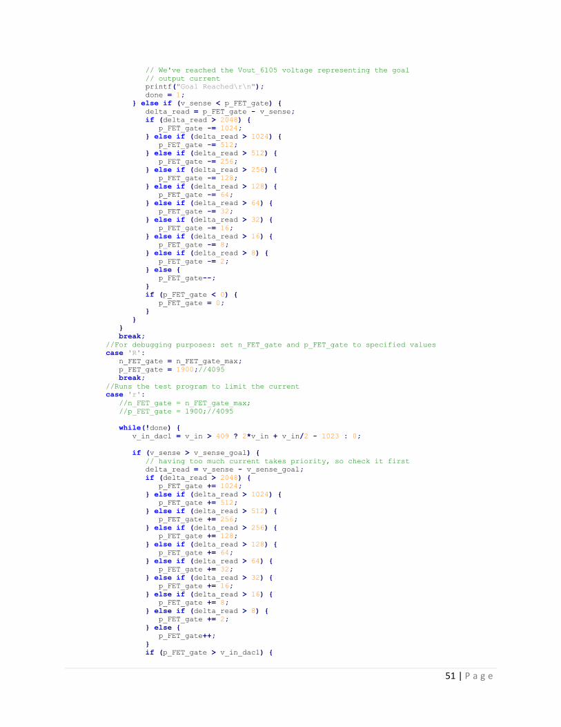
51 | P a g e
// We've reached the Vout_6105 voltage representing the goal
// output current
printf("Goal Reached\r\n");
done = 1;
} else if (v_sense < p_FET_gate) {
delta_read = p_FET_gate - v_sense;
if (delta_read > 2048) {
p_FET_gate -= 1024;
} else if (delta_read > 1024) {
p_FET_gate -= 512;
} else if (delta_read > 512) {
p_FET_gate -= 256;
} else if (delta_read > 256) {
p_FET_gate -= 128;
} else if (delta_read > 128) {
p_FET_gate -= 64;
} else if (delta_read > 64) {
p_FET_gate -= 32;
} else if (delta_read > 32) {
p_FET_gate -= 16;
} else if (delta_read > 16) {
p_FET_gate -= 8;
} else if (delta_read > 8) {
p_FET_gate -= 2;
} else {
p_FET_gate--;
}
if (p_FET_gate < 0) {
p_FET_gate = 0;
}
}
}
break;
//For debugging purposes: set n_FET_gate and p_FET_gate to specified values
case 'R':
n_FET_gate = n_FET_gate_max;
p_FET_gate = 1900;//4095
break;
//Runs the test program to limit the current
case 'r':
//n_FET_gate = n_FET_gate_max;
//p_FET_gate = 1900;//4095
while(!done) {
v_in_dac1 = v_in > 409 ? 2*v_in + v_in/2 - 1023 : 0;
if (v_sense > v_sense_goal) {
// having too much current takes priority, so check it first
delta_read = v_sense - v_sense_goal;
if (delta_read > 2048) {
p_FET_gate += 1024;
} else if (delta_read > 1024) {
p_FET_gate += 512;
} else if (delta_read > 512) {
p_FET_gate += 256;
} else if (delta_read > 256) {
p_FET_gate += 128;
} else if (delta_read > 128) {
p_FET_gate += 64;
} else if (delta_read > 64) {
p_FET_gate += 32;
} else if (delta_read > 32) {
p_FET_gate += 16;
} else if (delta_read > 16) {
p_FET_gate += 8;
} else if (delta_read > 8) {
p_FET_gate += 2;
} else {
p_FET_gate++;
}
if (p_FET_gate > v_in_dac1) {
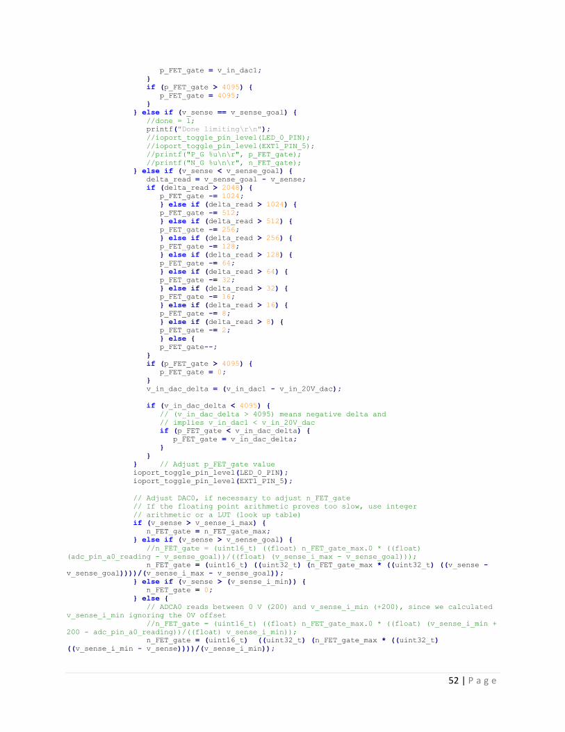
52 | P a g e
p_FET_gate = v_in_dac1;
}
if (p_FET_gate > 4095) {
p_FET_gate = 4095;
}
} else if (v_sense == v_sense_goal) {
//done = 1;
printf("Done limiting\r\n");
//ioport_toggle_pin_level(LED_0_PIN);
//ioport_toggle_pin_level(EXT1_PIN_5);
//printf("P_G %u\n\r", p_FET_gate);
//printf("N_G %u\n\r", n_FET_gate);
} else if (v_sense < v_sense_goal) {
delta_read = v_sense_goal - v_sense;
if (delta_read > 2048) {
p_FET_gate -= 1024;
} else if (delta_read > 1024) {
p_FET_gate -= 512;
} else if (delta_read > 512) {
p_FET_gate -= 256;
} else if (delta_read > 256) {
p_FET_gate -= 128;
} else if (delta_read > 128) {
p_FET_gate -= 64;
} else if (delta_read > 64) {
p_FET_gate -= 32;
} else if (delta_read > 32) {
p_FET_gate -= 16;
} else if (delta_read > 16) {
p_FET_gate -= 8;
} else if (delta_read > 8) {
p_FET_gate -= 2;
} else {
p_FET_gate--;
}
if (p_FET_gate > 4095) {
p_FET_gate = 0;
}
v_in_dac_delta = (v_in_dac1 - v_in_20V_dac);
if (v_in_dac_delta < 4095) {
// (v_in_dac_delta > 4095) means negative delta and
// implies v_in_dac1 < v_in_20V_dac
if (p_FET_gate < v_in_dac_delta) {
p_FET_gate = v_in_dac_delta;
}
}
} // Adjust p_FET_gate value
ioport_toggle_pin_level(LED_0_PIN);
ioport_toggle_pin_level(EXT1_PIN_5);
// Adjust DAC0, if necessary to adjust n_FET_gate
// If the floating point arithmetic proves too slow, use integer
// arithmetic or a LUT (look up table)
if (v_sense > v_sense_i_max) {
n_FET_gate = n_FET_gate_max;
} else if (v_sense > v_sense_goal) {
//n_FET_gate = (uint16_t) ((float) n_FET_gate_max.0 * ((float)
(adc_pin_a0_reading - v_sense_goal))/((float) (v_sense_i_max - v_sense_goal)));
n_FET_gate = (uint16_t) ((uint32_t) (n_FET_gate_max * ((uint32_t) ((v_sense -
v_sense_goal))))/(v_sense_i_max - v_sense_goal));
} else if (v_sense > (v_sense_i_min)) {
n_FET_gate = 0;
} else {
// ADCA0 reads between 0 V (200) and v_sense_i_min (+200), since we calculated
v_sense_i_min ignoring the 0V offset
//n_FET_gate = (uint16_t) ((float) n_FET_gate_max.0 * ((float) (v_sense_i_min +
200 - adc_pin_a0_reading))/((float) v_sense_i_min));
n_FET_gate = (uint16_t) ((uint32_t) (n_FET_gate_max * ((uint32_t)
((v_sense_i_min - v_sense))))/(v_sense_i_min));
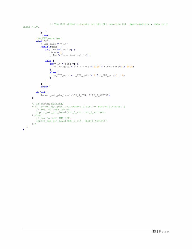
53 | P a g e
// The 200 offset accounts for the ADC reaching 200 (approximately), when it's
input = 0V.
}
}
break;
//n_FET_gate test
case '2':
n_FET_gate = v_in;
while(!done) {
if(v_in == seek_v) {
done = 1;
printf("Done Seeking\r\n");
}
else {
if(v_in < seek_v) {
n_FET_gate = n_FET_gate < 4095 ? n_FET_gate+1 : 4095;
}
else {
n_FET_gate = n_FET_gate > 0 ? n_FET_gate-1 : 0;
}
}
}
break;
default:
ioport_set_pin_level(LED_0_PIN, !LED_0_ACTIVE);
}
// is button pressed?
/*if (ioport_get_pin_level(BUTTON_0_PIN) == BUTTON_0_ACTIVE) {
// Yes, so turn LED on.
ioport_set_pin_level(LED_0_PIN, LED_0_ACTIVE);
} else {
// No, so turn LED off.
ioport_set_pin_level(LED_0_PIN, !LED_0_ACTIVE);
}*/
}
}

54 | P a g e
Appendix C – Component Purchase Invoices
Figure C-1: Digikey Invoice 1

55 | P a g e
Figure C-2: Digikey Invoice 1 Continued

56 | P a g e
Figure C-3: Digikey Invoice 1 Continued

57 | P a g e
Figure C-4: Digikey Invoice 2

58 | P a g e
Figure C-5: Digikey Invoice 3

59 | P a g e
Figure C-6: Digikey Invoice 4

60 | P a g e
Figure C-7: Digikey Invoice 5

61 | P a g e
Figure C-8: Digikey Invoice 6

62 | P a g e
Figure C-9: Mouser Invoice 1

63 | P a g e
Figure C-10: Mouser Invoice 2

64 | P a g e
Figure C-11: AVNET Invoice 1

65 | P a g e
Appendix D – Early Design Ideas
Figure D-1: Circuit Diagram for the Early Design of the Overvoltage Protection Circuit