prospective life cycle assessment of epitaxial...
TRANSCRIPT

R E S E A R C H A N D A N A LYS I S
Prospective Life Cycle Assessment ofEpitaxial Graphene Production at DifferentManufacturing Scales and MaturityRickard Arvidsson and Sverker Molander
Summary
Epitaxial growth is a potential production process for the new material graphene, where itis grown on silicon carbide (SiC) wafers at high temperatures. We provide first estimates ofthe life cycle cumulative energy demand, climate change, terrestrial acidification, and eco-toxicity of this production. For this purpose, we applied prospective life cycle assessment(LCA) for three production scenarios (lab, pilot, and an industrial scenario), which reflectdifferent production scales and technological maturity. The functional unit was one squarecentimeter of graphene. Results show that the three scenarios have similar impacts, whichgoes against previous studies that have suggested a decrease with larger production scaleand technological maturity. The reason for this result is the dominance of electricity usein the SiC wafer production for all impacts (>99% in the worst case, >76% in the bestcase). Only when assuming thinner SiC wafers in the industrial scenario is there a reductionin impacts by around a factor of 10. A surface-area–based comparison to the life cycleenergy use of graphene produced by chemical vapor deposition showed that epitaxialgraphene was considerably more energy intensive—approximately a factor of 1,000. Werecommend producers of epitaxial graphene to investigate the feasibility of thinner SiCwafers and use electricity based on wind, solar, or hydropower. The main methodologicalrecommendation from the study is to achieve a temporal robustness of LCA studies ofemerging technologies, which includes the consideration of different background systemsand differences in production scale and technological maturity.
Keywords:
energy consumptionepitaxial growthindustrial ecologyLCAnanomaterialsilicon carbide
Supporting information is linkedto this article on the JIE website
Introduction
Graphene is a one-carbon-atom-thin material that has beendescribed as a “wonder material” and as a “rising star on thehorizon of materials science” (Geim 2009, 1530; Geim andNovoselov 2007, 183). Although commercialization is yet lim-ited, graphene has been suggested for use in many different areas,such as energy production and storage, including batteries andfuel cells (Brownson et al. 2011); transparent electrodes in com-puter screens (Blake et al. 2008); semiconductors in electronics
Address correspondence to: Rickard Arvidsson, Division of Environmental Systems Analysis, Department of Energy and Environment, Chalmers University of Technology,Rannvagen 6, SE 412 96 Gothenburg, Sweden. Email: [email protected]
© 2016 The Authors. Journal of Industrial Ecology, published by Wiley Periodicals, Inc., on behalf of Yale University. This is an open access article under the terms of theCreative Commons Attribution License, which permits use, distribution and reproduction in any medium, provided the original work is properly cited.DOI: 10.1111/jiec.12526 Editor managing review: Michael Hauschild
Volume 21, Number 5
(Van Noorden 2006); reinforcement in composite materials (Liand Zhong 2011); and environmental applications, such as wa-ter purification (Shen et al. 2015). In order for graphene to beable to fulfill these promises, feasible and environmentally be-nign production processes are required. According to a patentanalysis, there are currently three main production processesbeing developed toward large-scale production, namely, exfoli-ation, chemical vapor deposition (CVD), and epitaxial growth(Sivudu and Mahajan 2012).
www.wileyonlinelibrary.com/journal/jie Journal of Industrial Ecology 1153

R E S E A R C H A N D A N A LYS I S
In exfoliation processes, graphene sheets can be exfoliatedfrom graphite by ultrasound or thermal treatment. Anothertype of exfoliation is by oxidation of graphite, during whichelectrostatic repulsion facilitates separation of the graphenesheets, followed by reduction to remove the oxygen. Exfoliationprocesses provide graphene sheets suspended in wet solution.Environmental impacts from ultrasound and oxidation pro-cesses have been assessed in a life cycle assessment (LCA) studyby Arvidsson and colleagues (2014), who concluded that the ul-trasound process was environmentally preferable provided thatthe solvent could be efficiently recovered and reused. Such effi-cient production by ultrasound may have as low an energy use as70 megajoules per kilogram (MJ/kg), whereas the oxidationprocess required at least 800 MJ/kg. Pizza and colleagues(2014) assessed life cycle impacts from a graphene-containingcomposite material, with graphene produced by thermaltreatment. They found graphene produced by this processto be relatively energy intensive—almost 2,000 MJ/kg. Themass-based functional units of these studies are reflectionsof the form of graphene obtained from exfoliation processes:powders or sheets suspended in liquid. The currently mostlikely future application for exfoliated graphene is in compositematerials (Sivudu and Mahajan 2012).
In CVD, graphene is obtained by depositing carbon-containing gases onto a metal catalyst at high temperature.Contrary to exfoliated graphene, CVD-grown graphene is notobtained as a suspension, but as a thin surface layer. Grapheneproduced by CVD is primarily suggested for use in transparentelectrodes that can be used in displays (Blake et al. 2008). Theproduction of graphene-based electrodes by CVD was assessedby Arvidsson and colleagues (2016), who found that such elec-trodes could be preferable to the currently used material (indiumtin oxide) from a life cycle energy use perspective, given thatthe input of the raw material, methane, is low. Such low-inputCVD of graphene may require as little as 7 kilojoules per squarecentimeter (kJ/cm2), whereas indium tin oxide production re-quires 20 to 70 kJ/cm2. In addition, by using graphene insteadof indium tin oxide, the scarce material, indium, can be sub-stituted by carbon, which is beneficial from an abiotic resourcedepletion perspective (Arvidsson et al. 2016).
Similarly to CVD, epitaxial growth provides graphene inthe form of a thin surface layer. Graphene produced by epitax-ial growth has been suggested as a potential substitute for siliconas semiconductor material in microchips (Van Noorden 2006;Zhou et al. 2007) and as a biosensor, which could be used to in-dicate cancer and other diseases (Tehrani et al. 2014). Epitaxialgraphene is suggested as suitable for these applications becauseof its high quality and because it can be grown directly on sil-icon carbide (SiC) semiconductor substrates without any needfor transfer (Novoselov et al. 2012; Sivudu and Mahajan 2012;Hertel et al. 2012). To our knowledge, this article representsthe first LCA of epitaxial graphene production.
The main challenge when conducting an assessment of thisprocess is that no large-scale production yet exists. This im-plies the need to use prospective LCA methodology in orderto assess future potential environmental impacts of epitaxial
graphene production. In the LCA field, the term prospectivewas first used to denote what is today referred to as consequen-tial (change-oriented) LCA (Tillman 2000). However, it is nowacknowledged that prospective LCA is not related to the dis-tinction between consequential and attributional (accounting)LCA (Hillman and Sanden 2008; Sanden and Karlstrom 2007;Herrmann et al. 2014). Prospective LCA is used to assess prod-ucts at an early stage of technological development, but withthe aim of encompassing future environmental impacts.
Several researchers have highlighted challenges that arisewhen conducting prospective LCA studies. Hillman andSanden (2008) discussed the implications of scale and changesin background systems when assessing emerging technologies.They showed that these aspects could alter the environmen-tal impact of ethanol and rapeseed methyl ester fuel consid-erably. Hetherington and colleagues (2014) identified severalchallenges for LCA studies of emerging technologies, includingscale of production, data availability, unknown future applica-tions, and challenges for comparability, given that emergingtechnologies may not be functionally equivalent to those theyreplace. Although this last challenge relating to comparabilityalso exists in conventional LCA, it becomes more fundamen-tal in prospective LCA (Hetherington et al. 2014). Gavankarand colleagues (2014) highlighted the importance of consid-ering production scale and technological maturity when as-sessing emerging technologies. They suggested manufacturingreadiness level (MRL) as an indicator of the level of techno-logical maturity. MRL is indicated on an ordinal scale from1 (research identified for material properties, manufacturing,cost implications, and investments) to 10 (large-scale produc-tion) (US DoD 2015). Wender and colleagues (2014) criticizedpoint-value estimations of environmental impacts for emerg-ing technologies considering the inherent data uncertainty andinstead recommended uncertainty analysis strategies. In theirprospective LCA study of graphene produced by ultrasonicationand chemical reduction, Arvidsson and colleagues (2014) fur-ther highlighted the influence of background system life cycleimpacts, which can vary considerably. Some of these aspects,generic to LCA studies of immature products in general, arealso mentioned in some reviews of LCA studies of nanomateri-als (Gavankar et al. 2012; Arvidsson 2015).
In this article, the main recommendations from these stud-ies will be considered in order to conduct a prospective LCAof epitaxial graphene production. These recommendations areto consider: (1) parameter uncertainties and avoid point-valueestimations (Wender et al. 2014; Arvidsson 2015); (2) the in-creased efficiency of production scale and technological matu-rity (Gavankar et al. 2014; Hillman and Sanden 2008; Hether-ington et al. 2014; Gavankar et al. 2012); and (3) different back-ground systems, such as electricity production (Hillman andSanden 2008; Arvidsson et al. 2014). Accordingly, the articleaims to assess environmental impacts from epitaxial growth ofgraphene in a way that (1) includes a thorough sensitivity analy-sis of parameter uncertainties, (2) takes into account productionscale and technological maturity, and (3) includes a thoroughinvestigation of the impacts of different background systems.
1154 Journal of Industrial Ecology

R E S E A R C H A N D A N A LYS I S
Silicon layer
Carbon layer
Silicon carbide (SiC) wafer
Graphene
Heating
Sublimated silicon
Figure 1 Schematic representation of the epitaxial graphene growth process.
This is performed by using three production scenarios for epitax-ial graphene production (lab, pilot, and industrial) as well as bestand worst cases for parameter values and background systems.
Method
System Description and Functional Unit
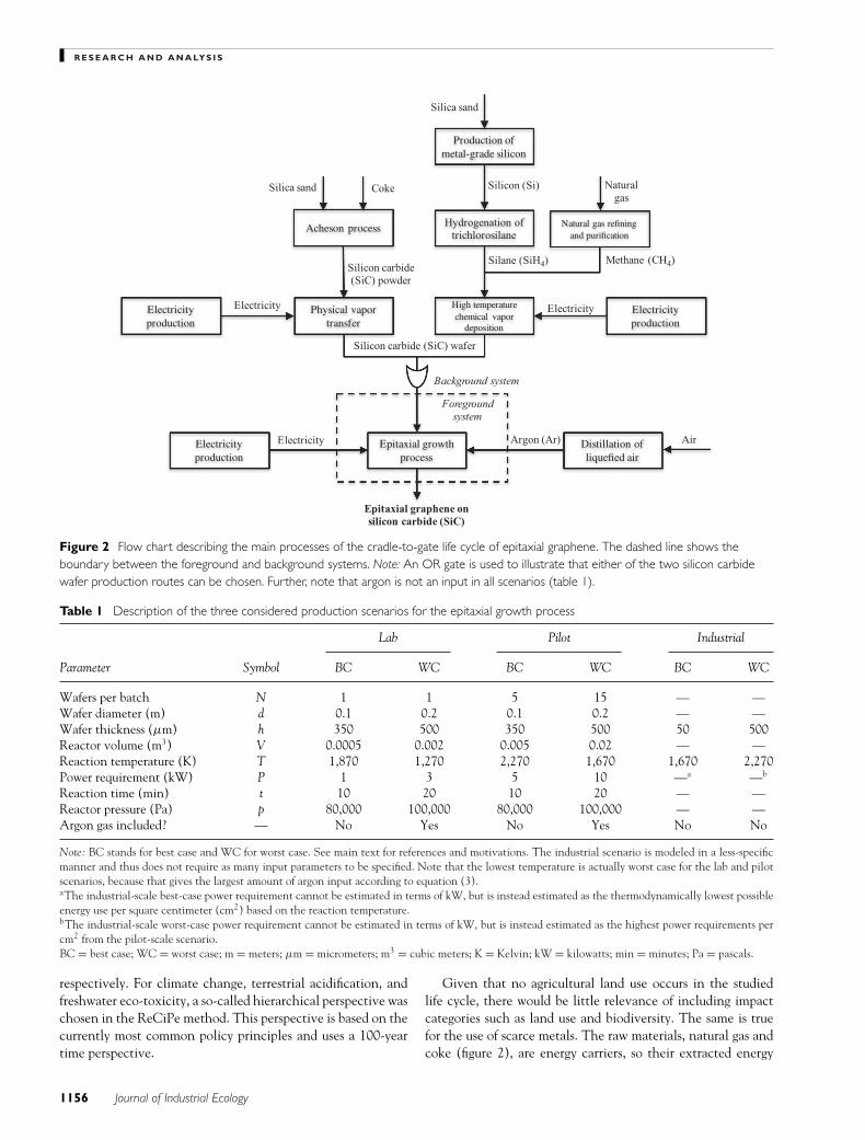
Epitaxial growth of graphene is the foreground system of thisstudy. As described in a number of studies (de Heer et al. 2011;Virojanadara et al. 2008; Emtsev et al. 2009), epitaxial growth ofgraphene takes place in a reactor where cylindrical SiC wafersare placed. SiC wafers consist of one-atom-thick alternatinglayers of silicon and carbide. The epitaxial process occurs undera high temperature that makes the silicon sublimate, and followsthis principal reaction:
SiC(s) → C(s) + Si(g) (R1)
The solid carbon in R1, which is left after the silicon sub-limation, forms carbon-carbon bonds and becomes graphene.The entire topside of the SiC wafer becomes covered by one orperhaps a few graphene layers. Figure 1 illustrates the epitax-ial growth process. The formed graphene layer prevents furthersilicon sublimation, and the reaction is thus self-limiting (deHeer et al. 2007). Given that the output of the epitaxial growthis a surface area of graphene, the functional unit of the study is1 cm2 of epitaxial graphene.
In preference, the epitaxial growth process is run in batches.With a continuous process, convection at the SiC-graphene sur-face could occur, leading to increased silicon sublimation rates.High silicon sublimation rates have been shown to adversely af-fect graphene quality (Yakimova et al. 2013; Virojanadara et al.2008; Emtsev et al. 2009). There are three possible inputs to theepitaxial growth process: the SiC wafer, electricity for heating,and argon gas (figure 2). The SiC wafer is the source of carbon,heat is required for the silicon to sublimate, and the argon can beapplied in order to create a counter pressure that reduces siliconsublimation rates and thereby ensures higher graphene quality.
Scenario Analysis
Three different foreground system scenarios have been con-sidered. These represent different production scales and levelsof technological maturity for the epitaxial growth process. The
first scenario is the lab scenario, which represents current labproduction. The second scenario is the pilot scenario, whichrepresents current small-scale production. The third scenario isthe industrial scenario, where assumptions about future processsettings are used in order to obtain an estimate of an efficientlarge-scale production. Process settings for the three productionscenarios are shown in table 1 and are further described in de-tail in sections titled Lab Scenario, Pilot Scenario, and IndustrialScenario.
Rather than providing point-value estimations, we use best-and worst-case estimates for the three production scenarios.This is motivated by the current immature state of epitaxialgraphene technology and the associated inherent uncertaintiesregarding its future production system. To ensure transparency(Pauliuk et al. 2015), we provide equations that show how allinputs to the epitaxial graphene growth were calculated andsources for all input data, thus enabling the reproduction andfuture updating of our results.
Impact Categories
It was known beforehand that high temperatures are requiredin epitaxial growth, and that SiC wafers are energy-intensivematerials. Therefore, three impact categories related to energyuse and impacts from energy use were chosen. The first was thecumulative energy demand (CED), as described by Hischier andcolleagues (2010), and reported in MJ. This indicator includesall types of energy, both renewable and nonrenewable, as theyare extracted from nature. The second was climate change asdescribed in the ReCiPe impact assessment method (Goedkoopet al. 2013). Climate change was estimated in kilograms (kg)carbon dioxide (CO2) equivalents (eq). The third chosen wasterrestrial acidification, again according to the ReCiPe impactassessment method (Goedkoop et al. 2013), and reported in kgsulfur dioxide (SO2) eq. In addition, we include eco-toxicitycalculated by two different methods. The first method is thefreshwater eco-toxicity included in the ReCiPe impact assess-ment method (Goedkoop et al. 2013), which is based on theUSES-LCA method (Huijbregts et al. 2000). The second isthe eco-toxicity included in the USEtox method (version 1)(Rosenbaum et al. 2008; Hauschild et al. 2008). The impactis estimated in kg 1,4-dichlorobenzene (1,4-DCB) and cumu-lative toxic units for eco-toxicity (CTUe) in these methods,
Ar vidsson and Molander, Prospective LCA of Epitaxial Graphene 1155
R E S E A R C H A N D A N A LYS I S
Epitaxial growth process
Physical vapor transfer
Electricity production
Distillation of liquefied air
Epitaxial graphene on silicon carbide (SiC)
Argon (Ar)Electricity
High temperature chemical vapor
deposition
Silicon carbide (SiC) wafer
Electricity production
Electricity Electricity production
Electricity
Acheson process
Silicon carbide (SiC) powder
Hydrogenation of trichlorosilane
Natural gas refining and purification
Methane (CH4)Silane (SiH4)
Production of metal-grade silicon
Silicon (Si)Silica sand
Silica sand
Air
Coke Natural gas
Background system
Foreground system
Figure 2 Flow chart describing the main processes of the cradle-to-gate life cycle of epitaxial graphene. The dashed line shows theboundary between the foreground and background systems. Note: An OR gate is used to illustrate that either of the two silicon carbidewafer production routes can be chosen. Further, note that argon is not an input in all scenarios (table 1).
Table 1 Description of the three considered production scenarios for the epitaxial growth process
Lab Pilot Industrial
Parameter Symbol BC WC BC WC BC WC
Wafers per batch N 1 1 5 15 — —Wafer diameter (m) d 0.1 0.2 0.1 0.2 — —Wafer thickness (μm) h 350 500 350 500 50 500Reactor volume (m3) V 0.0005 0.002 0.005 0.02 — —Reaction temperature (K) T 1,870 1,270 2,270 1,670 1,670 2,270Power requirement (kW) P 1 3 5 10 —a —b
Reaction time (min) t 10 20 10 20 — —Reactor pressure (Pa) p 80,000 100,000 80,000 100,000 — —Argon gas included? — No Yes No Yes No No
Note: BC stands for best case and WC for worst case. See main text for references and motivations. The industrial scenario is modeled in a less-specificmanner and thus does not require as many input parameters to be specified. Note that the lowest temperature is actually worst case for the lab and pilotscenarios, because that gives the largest amount of argon input according to equation (3).aThe industrial-scale best-case power requirement cannot be estimated in terms of kW, but is instead estimated as the thermodynamically lowest possibleenergy use per square centimeter (cm2) based on the reaction temperature.bThe industrial-scale worst-case power requirement cannot be estimated in terms of kW, but is instead estimated as the highest power requirements percm2 from the pilot-scale scenario.BC = best case; WC = worst case; m = meters; μm = micrometers; m3 = cubic meters; K = Kelvin; kW = kilowatts; min = minutes; Pa = pascals.
respectively. For climate change, terrestrial acidification, andfreshwater eco-toxicity, a so-called hierarchical perspective waschosen in the ReCiPe method. This perspective is based on thecurrently most common policy principles and uses a 100-yeartime perspective.
Given that no agricultural land use occurs in the studiedlife cycle, there would be little relevance of including impactcategories such as land use and biodiversity. The same is truefor the use of scarce metals. The raw materials, natural gas andcoke (figure 2), are energy carriers, so their extracted energy
1156 Journal of Industrial Ecology

R E S E A R C H A N D A N A LYS I S
content is accounted for by the CED indicator. However, sil-ica sand is also an important raw material in epitaxial grapheneproduction (figure 2), and the scarcity of silica sand is of growingconcern (Peduzzi 2014). Moreover, there is a lack of consensuson nonenergy abiotic resource impact assessment methods inLCA (Klinglmair et al. 2014; Drielsma et al. 2016) and a lackof characterization factors for silica sand in contemporary re-source impact assessment methods. Resource aspects related tothe use of silica sand are therefore discussed qualitatively in thePotential Silica Sand Scarcity section instead, following the rec-ommendation of the International Reference Life Cycle DataSystem (ILCD) handbook (EC-JRC 2011).
Inventory Analysis
Lab Scenario
The lab scenario is based on descriptions and data from anumber of publications from the Epitaxial Graphene Lab atGeorgia Institute of Technology in the United States. In theirstudies, this pioneering group refers to their process as confinedcompartment sublimation (de Heer et al. 2011; Ruan et al. 2012;Ruan 2012; Li 2008). They typically produce one wafer perbatch. The SiC wafer is reported to be bought from Cree Inc.,and this company sells SiC wafers with thicknesses between350 and 500 micrometers (μm) (Cree Inc. 2015). Diameters ofwafers sold are 0.15 meters (m) (Cree Inc. 2015), so a rangeof 0.1 to 0.2 m is used here. Photographs of the equipment inthe studies indicate a reactor volume of approximately 0.001cubic meters (m3), so a range of 0.0005 to 0.002 m3 is usedin this study. Temperatures between 1,270 and 1,870 Kelvin(K) are reported. Induction heating is used for heat production,and they have used power requirements of 2 kilowatts (kW).A range of 1 to 3 kW is therefore used. Reaction times varybetween 10 and 20 minutes, and the reaction takes place atapproximately atmospheric pressure (80,000 to 100,000 pascals[Pa]).
The electricity required for heating was calculated as shownby equation (1):
Eel = Pt
Nπ( d
2
)2 [J/cm2] (1)
where Eel is the electric energy for heating, P is the powerrequirement of the induction heating, t is the reaction time, Nis the number of wafers per batch, and d is the wafer diameter.The amount of SiC wafer required was calculated as shown byequation (2):
mSiC = Nπ( d
2
)2h p
Nπ( d
2
)2 [kg/cm2] (2)
where h is the thickness of the wafer, and ρ is the density of SiC(3,210 kg/m3). The amount of argon required is calculated withthe aid of the ideal gas law, which works well for inert gasessuch as argon (equation 3):
mAr =(
MpVRT
)/(Nπ
(d2
)2)
[kg/cm2] (3)
where mAr is the mass of argon required, M is the molar massof argon (0.040 kg/mol), p is the reactor pressure, V is thereactor volume, R is the ideal gas law constant (8.31 joules[J]/K·mol), and T is the reactor temperature. In one variant ofthis production scenario, no argon is used to limit sublimationrates, but instead the sublimation rate of silicon is controlled bya reusable graphite enclosure (de Heer et al. 2011; Ruan 2012).This is considered in the sensitivity analysis of this productionscenario by excluding the environmental impact of argon in thebest case.
In some early studies from this group, hydrogen was usedto smooth the SiC wafer surface before the reaction in orderto obtain high-quality graphene. However, very smooth SiCwafers are now commercially available (Hass et al. 2008), so nohydrogen input is assumed in the lab scenario (nor in any otherscenario).
There should be no process emissions from the epitaxialgrowth, neither of graphene nor of other materials (Ali 2015).The process takes place in a confined reactor and the grapheneis bound to the SiC wafer. Silicon-containing gases leave thewafer surface during the reaction, but if the reactor is not openeduntil it regains room temperature, they will return to solid form.This applies for all three production scenarios.
Pilot Scenario
The recently installed production equipment at the com-pany Graphensic in Linkoping, Sweden, represents the pilotscenario. Information about this has been obtained from inter-views with representatives from Graphensic by telephone ande-mail (Ali 2015; Syvajarvi 2015; Nilsson 2015), one study oftheirs (Virojanadara et al. 2008), and from the patent describ-ing their process (Yakimova et al. 2013). The pilot productionprocess produces around 10 wafers per batch, so we use a rangeof 5 to 15 wafers per batch. The wafers used have a diameter of0.15 m, so the same range as in the lab scenario is used (0.1 to 0.2m). The thickness of the SiC wafers used is 500 μm, but a sizeof 350 μm is considered as a potential best case. The reactor hasa volume of approximately 0.01 m3, so a range of 0.005 to 0.02m3 is used here. The temperature is between 1,670 and 2,270K, and an induction furnace is used to provide heat at 5 to 10kW. The reaction time is similar to that of the lab scenario (10to 20 minutes). Argon is used to limit silicon sublimation rates,and the reactor pressure is reported to be 80,000 to 100,000 Pa(close to atmospheric pressure). However, we also test the ex-clusion of the argon as a best case as we did for the lab scenario.The amount of electricity, SiC wafer, and argon required arecalculated by equations (1), (2), and (3), respectively, in thesame manner as for the lab scenario.
Industrial Scenario
The industrial scenario is hypothetical and does not yet ex-ist. It should be seen as a what-if scenario (Borjesson et al.2006) of a future potential production. With regard to SiCwafer thickness, it is possible to produce layers as thin as
Ar vidsson and Molander, Prospective LCA of Epitaxial Graphene 1157

R E S E A R C H A N D A N A LYS I S
50 μm, although this is not currently the standard wafer sold byproducers (Syvajarvi 2015). For the best case, we assume herethat increased production of epitaxial graphene would spur thedevelopment toward thinner SiC wafers so that a thickness of50 μm is obtained. Such co-evolution of interdependent tech-nologies is not uncommon (Grubler 1998; Unruh 2000). Forthe worst case, we assume a thickness of 500 μm, which rep-resents the possibility that no such co-evolution takes place.The same temperature range of 1,670 to 2,270 K as for the pilotscenario is assumed.
The amount of SiC wafer required was calculated by equa-tion (2) in the same manner as for the lab and pilot scenarios.Regarding heating, we assumed that no improvements in elec-tricity use take place with increased technological maturity forthe worst case of the industrial scenario and thus applied thehighest electricity use of the pilot-scale scenario (30 kJ/cm2).For the best case, we assumed the lowest possible amount of en-ergy that could be required. This energy is modeled by the heatequation as the heat required for increasing the temperature ofthe SiC wafer’s mass from room temperature to the requiredreaction temperature (equation 4):
Eheat = Cp mSiC�T [J/cm2] (4)
where Eheat is the required heat for the temperature change, cp isthe heat capacity of the SiC (750 J/kg·K), mSiC is the mass of theSiC wafer required per functional unit (calculated by equation2), and �T is the temperature change. In addition to this energyrequired to increase the temperature, some energy for sublimat-ing the silicon would be required. However, because only oneor a few top layers of silicon are sublimated, this contribution tothe energy use is minor and therefore omitted. By this modeling,it is assumed that the electric heating is 100% efficient evenfor such high temperatures (i.e., no heat losses when convertingelectricity to heat are assumed). It is further assumed that the re-actor will be so well isolated and the reaction time shortened sothat energy losses will effectively be none. In effect, this meansa >95% electricity reduction per functional unit compared tothe lab and pilot scenarios. This is of similar magnitude as someother energy efficiency improvements suggested in the LCAliterature. For example, Li and colleagues (2013) assumed thatthe electricity use of nanofibrilated cellulose production wouldbe reduced by 92% from lab scale to industrial production, andalso note that this is actually a lower degree of reduction thansome other estimations. Moreover, for carbon nanotube pro-duction, a review by Gavankar and colleagues (2014) revealedenergy-use reductions of >99.9% when going from MRL 4 to 7to MRL 10.
Given that it is technically possible to prevent rapid silicongas sublimation without the continuous addition of materials(de Heer et al. 2011), the argon gas is excluded in the industrialscenario.
Silicon Carbide Wafer Production
SiC wafers are the substrate upon which the epitaxialgraphene grows, and their production is part of the background
system. The two main industrial processes currently used toproduce high-quality SiC wafers are physical vapor transport(PVT; also called seeded sublimation or modified Lely process)and high-temperature chemical vapor deposition (HTCVD).PVT is the standard process in industry today, although thenewer HTCVD has been gaining interest from industry (Wi-jesundara and Azevedo 2011; Yakimova and Janzen 2000). Inseveral studies describing lab-scale production of graphene, SiCwafers were obtained from Cree Inc. (Berger et al. 2004; Hasset al. 2006; Song 2006; Sprinkle 2010; Ruan 2012), and thiscompany has been reported to use the PVT process (Yakimovaand Janzen 2000). The company Norstel AB is providing SiCwafers for the pilot-scale production by Graphensic, and theyproduce SiC wafers by both of these two processes. Conse-quently, both of these SiC wafer production processes weretested for the three production scenarios.
Physical Vapor TransportIn standard PVT, a crude SiC source material is vaporized at
high temperature and the formed silicon and carbon gases areredeposited onto a high-quality SiC seed material (Wijesundaraand Azevedo 2011). Given the right conditions in terms oftemperature and pressure, and a high-quality seed crystal, SiCwill expand on the addition of the gases. The quality of theexpanding crystal will be that of the high-quality seed crystal.
Warren and colleagues (2015) estimated the electricity re-quired for producing a SiC substrate with the PVT process tobe 4.0 kilowatt-hours (kWh)/cm2 (15 MJ/cm2). This appliesfor a 350-μm wafer thickness and was linearly extrapolated forother thicknesses in this study. In addition to electricity, thereare two input materials for the PVT process—argon and thesource material—which is typically a low-quality SiC powder(Yakimova and Janzen 2000). Although an excess amount ofSiC powder is generally used to create an oversaturated envi-ronment, unused powder could be reused. Losses attributed todiscarding of poor-quality parts, slicing and polishing of SiCwafers are considered, giving a yield of 0.35 according to War-ren and colleagues (2015). Data for production of low-qualitySiC powder by the standard Acheson process was obtained fromthe ecoinvent version 2.2 database (ecoinvent 2010) (data postnumber 321). No data on how much argon is required havebeen found. We consider it likely that the production of argonhas much lower impacts than do the production of electricityand SiC powder. For example, the argon production’s CED perkg is only 4% of that of SiC powder production according tothe ecoinvent version 2.2 database (ecoinvent 2010) (data postnumbers 321 and 251, respectively). Because of the lack of dataand presumed minor influence, we have therefore excluded theargon in the PVT process. Because no data on process emissionsfrom SiC production by PVT were found, it had to be assumedthat such emissions are negligible.
High Temperature Chemical Vapor DepositionSimilar to the PVT process, the HTCVD process includes
the growth of a seed crystal (Wijesundara and Azevedo 2011).The two precursors are the gases silane (SiH4) and hydrocarbon.
1158 Journal of Industrial Ecology

R E S E A R C H A N D A N A LYS I S
The hydrocarbon could be either methane (CH4), ethane, orpropane (Wijesundara and Azevedo 2011), but is here assumedto be:
SiH4(g) + CH4(g) → SiC(s) + 4H2(g) (R2)
These gases are also used in excess, but could be recirculated,and the yield is equal to 0.5 attributable to slicing and polishingof the SiC wafer according to Warren and colleagues (2015).The hydrogen gas produced according to R2 is diluted and can-not be used for other purposes and therefore is assumed to beemitted to air. Data on production of methane in the form ofnatural gas is available in the ecoinvent version 2.2 database(ecoinvent 2010) (data post number 11053). Further electricityrequirement for purifying the methane was estimated to require0.21 to 2.5 MJ of electricity per kg by Arvidsson and colleagues(2016). The two extremes of this range are used in the best andworst cases, respectively. Silane can be produced by hydrogena-tion of trichlorosilane, and impacts from this process are avail-able in the ecoinvent version 2.2 database (ecoinvent 2010)(data post number 7210). In addition, Warren and colleagues(2015) estimated the electricity use of the HTCVD process it-self to be 2.8 kWh/cm2 (10 MJ/cm2) for a 350-μm wafer, whichwas again scaled linearly for other wafer thicknesses. Becauseno data on process emissions from SiC production by HTCVDwere found, it again had to be assumed that such emissions arenegligible.
Argon Gas Production
Argon gas production is part of the background system andtypically occurs by liquefying air and then separating the gases(nitrogen, oxygen, and argon) by distillation based on theirdiffering boiling points. Impacts from its production are reportedin the ecoinvent version 2.2 database (ecoinvent 2010) (datapost number 251). Allocation between the gases in air wasbased on the extent to which the specific gases contributed tothe energy requirement of air liquefaction.
Electricity Production
Epitaxial growth, SiC wafer production, and methane pu-rification require electricity, of which production is part of thisstudy’s background system. In a prospective LCA study, it isimportant to not only consider current electricity production,but also potential future electricity production systems, giventhat large differences in environmental impacts can occur be-tween different systems (Hillman and Sanden 2008). This isespecially important because the locations of future productionfacilities for graphene, SiC wafers, and methane are inherentlyunknown. In line with the general setup of the study, best andworst cases were considered.
For the three impact categories considered, electricity fromwind, solar, and hydropower typically have low impacts,whereas coal power has high impacts (Hertwich et al. 2015).The best case was thus taken to be the electricity mix of Nor-way, which has more than a 95% share of hydropower. Note
that electricity mixes based on solar and wind power, and com-binations of these three power sources, give similar impacts perMJ of electricity. The worst case is taken to be the electricitymix of Poland, which consists of more than 90% coal power.Similarly, data for other electricity mixes primarily based oncoal power give similar impacts per MJ of electricity. This in-cludes China, whose mix has around 80% coal power. Datafor these electricity mixes were obtained from the ecoinventversion 2.2 database (ecoinvent 2010) (data post numbers 657and 659, respectively). Notably, the CED of Norwegian elec-tricity is lower than that of the Polish electricity by around afactor of 3, whereas climate change is approximately 90 timeslower, terrestrial acidification is approximately 200 times lower,freshwater eco-toxicity based on ReCiPe is approximately 100times lower, and eco-toxicity based on USEtox is approximately30 times lower.
Transport
Including impacts from transport in prospective LCA is diffi-cult, given that the location or future production processes andmodes of transport are inherently unknown (Arvidsson et al.2014, 2015, 2016). The mass that could potentially be trans-ported is the combined mass of the SiC wafer, argon, and mate-rials for SiC production (SiC powder, or silane and methane).Again, in this study, best and worst cases were used.
In the best case, transport impacts were assumed to be effec-tively nonexistent. This would correspond to production withina local industrial cluster or eco-industrial park.
Savy and Burnham (2013) provided average transport dis-tances for product groups in the United States. These rangefrom crushed stone, which is transported approximately 60 kilo-meters (km), on average, to textiles and leather, which aretransported approximately 2,000 km on average. To representa worst case, the same average transport distance as for textilesand leather was assumed for the combined mass of the above-mentioned input materials. Transport was assumed to be oneway by truck. The truck was assumed to be a 2005 fleet averagecapable of carrying more than 28 metric tonnes, as described inthe ecoinvent version 2.2 database (ecoinvent 2010) (data postnumber 1944). This corresponds to a relatively polluting modeof transport, which is appropriate for a worst case.
Results and Discussions
Impact Category Results and Discussion
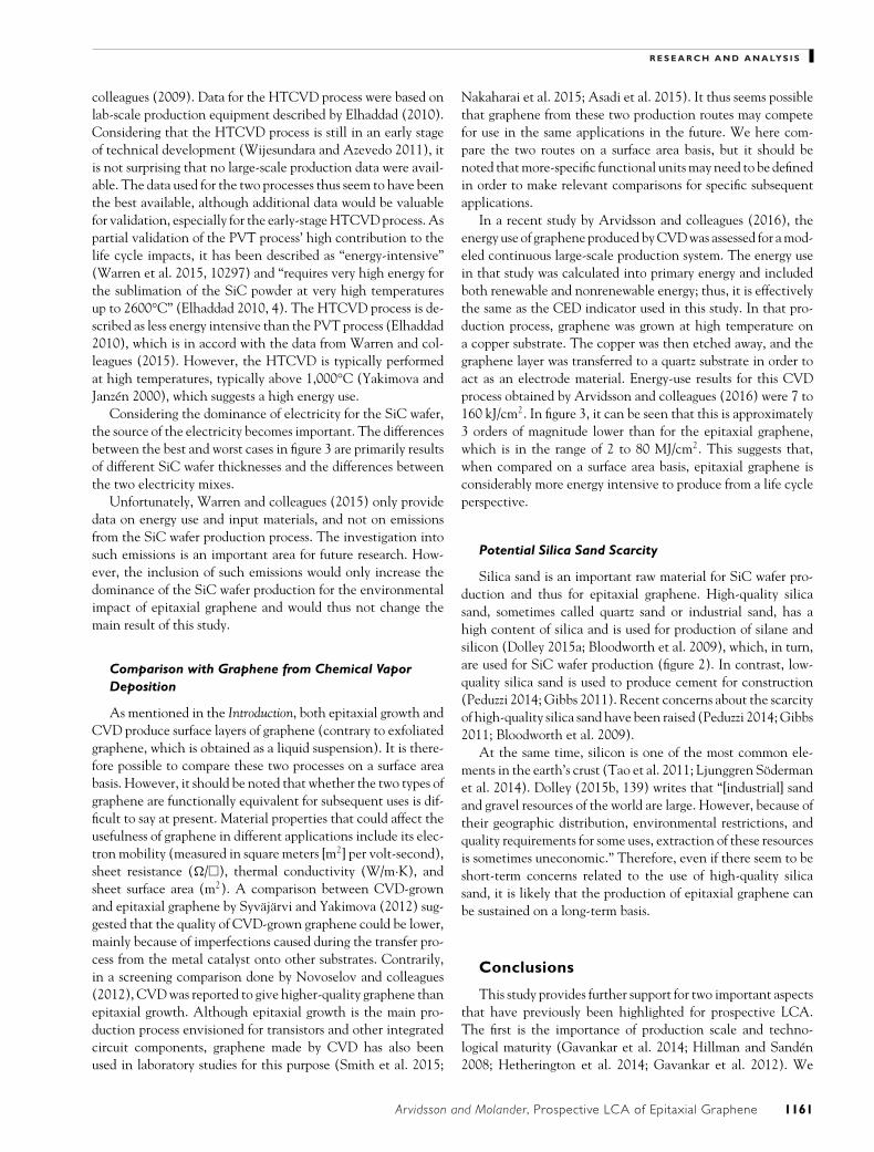
The results of this study are presented as best-case and worst-case environmental impacts for each of the production scenariosalong a technological scale and maturity axis, forming an en-vironmental impact area suggested to contain a wide range ofoutcomes. Figure 3 shows the results for CED, climate change,and terrestrial acidification, respectively. The graphs have sim-ilar shapes for all four impact categories. Between the lab andpilot scenarios, impacts are of the same order of magnitude.Between the pilot and industrial scenarios, impacts decrease by
Ar vidsson and Molander, Prospective LCA of Epitaxial Graphene 1159
R E S E A R C H A N D A N A LYS I S
Figure 3 Results for the (a) cumulative energy demand (CED), (b) climate change, (c) terrestrial acidification, and (d) eco-toxicity impactcategories. Squares show worst cases, and triangles show best cases. Note the logarithmic scales on (b), (c), and (d). In (d), white markersshow results for freshwater eco-toxicity based on ReCiPe (left axis), and black markers show results for eco-toxicity based on USEtox (rightaxis). 1,4-DCB = 1,4-dichlorobenzene; CTUe = cumulative toxic units for eco-toxicity; g SO2-eq/cm2 = grams sulfur dioxide equivalentsper square centimeter ; kg CO2-eq/cm2 = kilograms carbon dioxide equivalents per square centimeter ; MJ/cm2 = megajoules per squarecentimeter.
approximately 1 order of magnitude for the best case. This ispartly in accord with the findings of Gavankar and colleagues(2014), which suggested a clear decrease in environmental im-pacts as the production scale and technological maturity in-creased. The reduction in energy use in that study was shownto be several orders of magnitude for carbon nanotubes whengoing from an MRL corresponding to pilot scale to an MRLcorresponding to mass production. In this study, such reduc-tions in impact did not take place between the lab and pilotscenarios, and not between pilot and industrial scenarios forthe worst cases. The reason for this behavior is the dominanceof one factor in the background system for the environmentalimpacts: the electricity required to produce the SiC wafer. Thisaccounts for more than 99% of the impacts in the worst caseand more than 76% in the best case (see figures S1 to S5 in thesupporting information available on the Journal’s website). Inthe best case, silane production accounted for the other <24%of the impacts. Both these two major contributions are relatedto production of the SiC wafer.
The dominance of SiC wafer production for the impacts ex-plains the behavior of the graphs in figure 3. For the lab and
pilot scenarios, the SiC wafer thickness was 350 μm for thebest case and 500 μm for the worst case. The reason for the ap-proximately 10 times lower impacts of the industrial best-casescenario is that the SiC wafer thickness was reduced approxi-mately 10 times, from 350 to 500 to 50 μm.
This illustrates that the relationship outlined by Gavankarand colleagues (2014), suggesting that scaling up productionwill lead to reductions in impacts, may not apply in all cases.In the case of epitaxial graphene, there is a dominatingcontribution in the form of the SiC wafer. A scale-up willnot lead to any notable reductions in impacts unless thisdominating contribution is reduced during scale-up. In cases ofproducts with such dominating contributions, the relationshipbetween technological maturity and environmental impactsmay not follow the suggested trajectory.
Given that electricity use during SiC wafer production wasdominating, it is interesting to look closer at the original sourcesfor this data provided by Warren and colleagues (2015). For thePVT process, data on process steps were obtained from per-sonal communication with an industry consultant and energy-use data for each step were obtained from the article by Boyd and
1160 Journal of Industrial Ecology
R E S E A R C H A N D A N A LYS I S
colleagues (2009). Data for the HTCVD process were based onlab-scale production equipment described by Elhaddad (2010).Considering that the HTCVD process is still in an early stageof technical development (Wijesundara and Azevedo 2011), itis not surprising that no large-scale production data were avail-able. The data used for the two processes thus seem to have beenthe best available, although additional data would be valuablefor validation, especially for the early-stage HTCVD process. Aspartial validation of the PVT process’ high contribution to thelife cycle impacts, it has been described as “energy-intensive”(Warren et al. 2015, 10297) and “requires very high energy forthe sublimation of the SiC powder at very high temperaturesup to 2600°C” (Elhaddad 2010, 4). The HTCVD process is de-scribed as less energy intensive than the PVT process (Elhaddad2010), which is in accord with the data from Warren and col-leagues (2015). However, the HTCVD is typically performedat high temperatures, typically above 1,000°C (Yakimova andJanzen 2000), which suggests a high energy use.
Considering the dominance of electricity for the SiC wafer,the source of the electricity becomes important. The differencesbetween the best and worst cases in figure 3 are primarily resultsof different SiC wafer thicknesses and the differences betweenthe two electricity mixes.
Unfortunately, Warren and colleagues (2015) only providedata on energy use and input materials, and not on emissionsfrom the SiC wafer production process. The investigation intosuch emissions is an important area for future research. How-ever, the inclusion of such emissions would only increase thedominance of the SiC wafer production for the environmentalimpact of epitaxial graphene and would thus not change themain result of this study.
Comparison with Graphene from Chemical VaporDeposition
As mentioned in the Introduction, both epitaxial growth andCVD produce surface layers of graphene (contrary to exfoliatedgraphene, which is obtained as a liquid suspension). It is there-fore possible to compare these two processes on a surface areabasis. However, it should be noted that whether the two types ofgraphene are functionally equivalent for subsequent uses is dif-ficult to say at present. Material properties that could affect theusefulness of graphene in different applications include its elec-tron mobility (measured in square meters [m2] per volt-second),sheet resistance (�/�), thermal conductivity (W/m·K), andsheet surface area (m2). A comparison between CVD-grownand epitaxial graphene by Syvajarvi and Yakimova (2012) sug-gested that the quality of CVD-grown graphene could be lower,mainly because of imperfections caused during the transfer pro-cess from the metal catalyst onto other substrates. Contrarily,in a screening comparison done by Novoselov and colleagues(2012), CVD was reported to give higher-quality graphene thanepitaxial growth. Although epitaxial growth is the main pro-duction process envisioned for transistors and other integratedcircuit components, graphene made by CVD has also beenused in laboratory studies for this purpose (Smith et al. 2015;
Nakaharai et al. 2015; Asadi et al. 2015). It thus seems possiblethat graphene from these two production routes may competefor use in the same applications in the future. We here com-pare the two routes on a surface area basis, but it should benoted that more-specific functional units may need to be definedin order to make relevant comparisons for specific subsequentapplications.
In a recent study by Arvidsson and colleagues (2016), theenergy use of graphene produced by CVD was assessed for a mod-eled continuous large-scale production system. The energy usein that study was calculated into primary energy and includedboth renewable and nonrenewable energy; thus, it is effectivelythe same as the CED indicator used in this study. In that pro-duction process, graphene was grown at high temperature ona copper substrate. The copper was then etched away, and thegraphene layer was transferred to a quartz substrate in order toact as an electrode material. Energy-use results for this CVDprocess obtained by Arvidsson and colleagues (2016) were 7 to160 kJ/cm2. In figure 3, it can be seen that this is approximately3 orders of magnitude lower than for the epitaxial graphene,which is in the range of 2 to 80 MJ/cm2. This suggests that,when compared on a surface area basis, epitaxial graphene isconsiderably more energy intensive to produce from a life cycleperspective.
Potential Silica Sand Scarcity
Silica sand is an important raw material for SiC wafer pro-duction and thus for epitaxial graphene. High-quality silicasand, sometimes called quartz sand or industrial sand, has ahigh content of silica and is used for production of silane andsilicon (Dolley 2015a; Bloodworth et al. 2009), which, in turn,are used for SiC wafer production (figure 2). In contrast, low-quality silica sand is used to produce cement for construction(Peduzzi 2014; Gibbs 2011). Recent concerns about the scarcityof high-quality silica sand have been raised (Peduzzi 2014; Gibbs2011; Bloodworth et al. 2009).
At the same time, silicon is one of the most common ele-ments in the earth’s crust (Tao et al. 2011; Ljunggren Sodermanet al. 2014). Dolley (2015b, 139) writes that “[industrial] sandand gravel resources of the world are large. However, because oftheir geographic distribution, environmental restrictions, andquality requirements for some uses, extraction of these resourcesis sometimes uneconomic.” Therefore, even if there seem to beshort-term concerns related to the use of high-quality silicasand, it is likely that the production of epitaxial graphene canbe sustained on a long-term basis.
Conclusions
This study provides further support for two important aspectsthat have previously been highlighted for prospective LCA.The first is the importance of production scale and techno-logical maturity (Gavankar et al. 2014; Hillman and Sanden2008; Hetherington et al. 2014; Gavankar et al. 2012). We
Ar vidsson and Molander, Prospective LCA of Epitaxial Graphene 1161
R E S E A R C H A N D A N A LYS I S
have conducted a prospective LCA study of epitaxial grapheneproduction for three production scenarios: lab, pilot, and indus-trial. Results were only partly in agreement with the previouslyestablished relationship of reduced environmental impact withincreased production scale and technological maturity. Thissuggests that the scale-up behavior of emerging technologiesmay be case specific. The second aspect is the importance ofconsidering different background systems (Hillman and Sanden2008; Arvidsson et al. 2014). We noted that changes in theelectricity production background system had a considerableinfluence on the impacts of epitaxial graphene production.
These two aspects belong to the more general concept oftemporal robustness. For emerging technologies assessed inprospective LCA, there is a possibility that both foregroundand background systems will change with time. Although suchchanges can be difficult to anticipate, the assumption thatchange will not take place can be as difficult to validate asany other assumption. The main methodological recommen-dation from this study is thus to strive for temporal robust-ness when conducting prospective LCA studies. This was alsorecommended by Nordelof and colleagues (2014) following areview of LCA studies of hybrid, plug-in hybrid, and batteryelectric vehicles.
We have also shown that the impacts of epitaxial grapheneproduction are dominated by electricity for production of SiCwafers. Based on this, we recommend that producers of epitax-ial graphene investigate the feasibility of thinner SiC wafers,preferably produced by the less energy-intensive HTCVD pro-cess. We further recommend them to use electricity from wind,solar, or hydropower.
When compared to graphene made by the CVD process ona surface area basis, it was shown that epitaxial graphene pro-duction was more energy intensive by approximately a factor of1,000. Continued studies of the environmental impacts of thesetwo potential production processes for surface-bound grapheneare recommended in order to refine this preliminary compar-ison, for example, by taking into account material propertiesrelevant for specific subsequent applications.
Acknowledgments
The financial support from the Swedish Research Council forEnvironment, Agricultural Sciences and Spatial Planning (For-mas) and the Swedish Foundation for Strategic EnvironmentalResearch (Mistra) is gratefully acknowledged. We also thankAmer Ali, Mikael Syvajarvi, and Jonas Nilsson at Graphen-sic for providing valuable information and Matty Janssen forvaluable comments on the manuscript.
References
Ali, A. 2015. Personal communication with A. Ali, Chief ExecutiveOfficer at Graphensic, Linkoping, Sweden, between 23 March2015 and 6 November 2015.
Arvidsson, R. 2015. Life cycle assessment and risk assessment of man-ufactured nanomaterials. In Nanoengineering—Global approaches
to health and safety issues, edited by P. I. Dolez. Amsterdam:Elsevier.
Arvidsson, R., D. Nguyen, and M. Svanstrom. 2015. Life cycle assess-ment of cellulose nanofibrils production by mechanical treatmentand two different pretreatment processes. Environmental Science& Technology 49(11): 6881–6890.
Arvidsson, R., D. Kushnir, B. A. Sanden, and S. Molander. 2014.Prospective life cycle assessment of graphene production by ul-trasonication and chemical reduction. Environmental Science &Technology 48(8): 4529–4536.
Arvidsson, R., D. Kushnir, S. Molander, and B. A. Sanden. 2016.Energy and resource use assessment of graphene as a substitutefor indium tin oxide in transparent electrodes. Journal of CleanerProduction 132: 289–297.
Asadi, K., E. C. Timmering, T. C. T. Geuns, A. Pesquera, A. Cen-teno, A. Zurutuza, J. H. Klootwijk, P. W. M. Blom, and D.M. de Leeuw. 2015. Up-scaling graphene electronics by repro-ducible metal-graphene contacts. ACS Applied Materials & Inter-faces 7(18): 9429–9435.
Berger, C., Z. Song, T. Li, X. Li, A. Y. Ogbazghi, R. Feng, Z. Dai, et al.2004. Ultrathin epitaxial graphite: 2D electron gas propertiesand a route toward graphene-based nanoelectronics. The Journalof Physical Chemistry B 108(52): 19912–19916.
Blake, P., P. D. Brimicombe, R. R. Nair, T. J. Booth, D. Jiang, F.Schedin, L. A. Ponomarenko, et al. 2008. Graphene-based liquidcrystal device. Nano Letters 8(6): 1704–1708.
Bloodworth, A., D. Highley, R. Bate, D. Cameron, P. Lusty, and D.Rayner. 2009. Mineral planning fact sheet: Silica sand. London:British Geological Survey.
Borjesson, L., M. Hojer, K.-H. Dreborg, T. Ekvall, and G. Finnveden.2006. Scenario types and techniques: Towards a user’s guide.Futures 38(7): 723–739.
Boyd, S. B., A. Horvath, and D. Dornfeld. 2009. Life-cycleenergy demand and global warming potential of computa-tional logic. Environmental Science & Technology 43(19): 7303–7309.
Brownson, D. A. C., D. K. Kampouris, and C. E. Banks. 2011. Anoverview of graphene in energy production and storage applica-tions. Journal of Power Sources 196(11): 4873–4885.
Cree Inc. 2015. Cree silicon carbide substrates and epi-taxy. www.cree.com/˜/media/files/cree/chips-and-material/data-sheets-material/matcatalog.Pdf. Accessed 12 January 2015.
de Heer, W. A., C. Berger, M. Ruan, M. Sprinkle, X. Li, Y. Hu, B.Zhang, J. Hankinson, and E. Conrad. 2011. Large area and struc-tured epitaxial graphene produced by confinement controlled sub-limation of silicon carbide. Proceedings of the National Academy ofSciences of the United States of America 108(41): 16900–16905.
de Heer, W. A., C. Berger, X. Wu, P. N. First, E. H. Conrad, X. Li,T. Li, et al. 2007. Epitaxial graphene. Solid State Communications143(1–2): 92–100.
Dolley, T. P. 2015a. Minerals yearbook 2013: Silica. Reston, VA, USA:United States Geogogical Survey (USGS).
Dolley, T. P. 2015b. Mineral commodity summary 2015: Sand and gravel(industrial). Reston, VA, USA: United States Geological Survey(USGS).
Drielsma, J., A. Russell-Vaccari, T. Drnek, T. Brady, P. Weihed, M.Mistry, and L. Simbor. 2016. Mineral resources in life cycle impactassessment—Defining the path forward. The International Journalof Life Cycle Assessment 21(1): 85–105.
EC-JRC (European Commission-Joint Research Center). 2011. ILCDhandbook. Recommendations for life cycle impact assessment in
1162 Journal of Industrial Ecology

R E S E A R C H A N D A N A LYS I S
the European context. Luxemburg: Institute for Environment andSustainability.
ecoinvent. 2010. Version 2.2. www.ecoinvent.ch/. Accessed 16 Octo-ber 2015.
Elhaddad, A. 2010. Growth of SiC by high temperature CVD and appli-cation of thermo-gravimetry for an in-situ growth rate measurment.Essen, Germany: University of Duisburg-Essen.
Emtsev, K. V., A. Bostwick, K. Horn, J. Jobst, G. L. Kellogg, L. Ley,J. L. McChesney, et al. 2009. Towards wafer-size graphene layersby atmospheric pressure graphitization of silicon carbide. NatureMaterials 8(3): 203–207.
Gavankar, S., S. Suh, and A. Keller. 2012. Life cycle assessment atnanoscale: Review and recommendations. The International Jour-nal of Life Cycle Assessment 17(3): 295–303.
Gavankar, S., S. Suh, and A. A. Keller. 2014. The role of scale andtechnology maturity in life cycle assessment of emerging tech-nologies. Journal of Industrial Ecology 19(1): 51–60.
Geim, A. K. 2009. Graphene: Status and prospects. Science 324(5934):1530–1534.
Geim, A. K. and K. S. Novoselov. 2007. The rise of graphene. NatureMaterials 6(3): 183–191.
Gibbs, S. 2011. Sand shortage: Myth or reality? Modern Casting 101(7):28–31.
Goedkoop, M., R. Heijungs, M. Huijbregts, A. De Schryver, J. Struijs,and R. van Zelm. 2013. Recipe 2008. A life cycle impact assessmentmethod which comprises harmonised category indicators at the midpointand endpoint level. The Hague, the Netherlands: Dutch Ministryof Housing, Spatial Planning and Environment (VROM).
Grubler, A. 1998. Technology and global change. Cambridge, UK: Cam-bridge University Press.
Hass, J., W. A. de Heer, and E. H. Conrad. 2008. The growth andmorphology of epitaxial multilayer graphene. Journal of Physics:Condensed Matter 20(32): 323202.
Hass, J., R. Feng, T. Li, X. Li, Z. Zong, W. A. de Heer, P. N. First, E.H. Conrad, C. A. Jeffrey, and C. Berger. 2006. Highly orderedgraphene for two dimensional electronics. Applied Physics Letters89(14): 143106.
Hauschild, M. Z., M. Huijbregts, O. Jolliet, M. Macleod, M. Margni,D. van de Meent, R. K. Rosenbaum, and T. E. McKone. 2008.Building a model based on scientific consensus for life cycleimpact assessment of chemicals: The search for harmony andparsimony. Environmental Science & Technology 42(19): 7032–7037.
Herrmann, I. T., M. Z. Hauschild, M. D. Sohn, and T. E. McK-one. 2014. Confronting uncertainty in life cycle assessment usedfor decision support. Journal of Industrial Ecology 18(3): 366–379.
Hertel, S., D. Waldmann, J. Jobst, A. Albert, M. Albrecht, S. Re-shanov, A. Schoner, M. Krieger, and H. B. Weber. 2012. Tailoringthe graphene/silicon carbide interface for monolithic wafer-scaleelectronics. Nature Communications 3(957): 1–6.
Hertwich, E. G., T. Gibon, E. A. Bouman, A. Arvesen, S. Suh, G.A. Heath, J. D. Bergesen, A. Ramirez, M. I. Vega, and L. Shi.2015. Integrated life-cycle assessment of electricity-supply sce-narios confirms global environmental benefit of low-carbon tech-nologies. Proceedings of the National Academy of Sciences of theUnited States of America 112(20): 6277–6282.
Hetherington, A., A. Borrion, O. Griffiths, and M. McManus. 2014.Use of LCA as a development tool within early research: Chal-lenges and issues across different sectors. The International Journalof Life Cycle Assessment 19(1): 130–143.
Hillman, K. M. and B. A. Sanden. 2008. Time and scale in life cy-cle assessment: The case of fuel choice in the transport sector.International Journal of Alternative Propulsion 2(1): 1–12.
Hischier, R., B. Weidema, H.-J. Althaus, C. Bauer, G. Doka, R. Dones,R. Frischknecht, et al. 2010. Implementation of life cycle impactassessment methods data v2.2. St. Gallen, Sweden: Swiss Centerfor Life Cycle Inventories.
Huijbregts, M. A. J., U. Thissen, J. B. Guinee, T. Jager, D. Kalf, D.van De Meent, A. M. J. Ragas, A. Wegener Sleeswijk, and L.Reijnders. 2000. Priority assessment of toxic substances in lifecycle assessment. Part I: Calculation of toxicity potentials for 181substances with the nested multi-media fate, exposure and effectsmodel USES-LCA. Chemosphere 41(4): 541–573.
Klinglmair, M., S. Sala, and M. Brandao. 2014. Assessing resource de-pletion in LCA: A review of methods and methodological issues.The International Journal of Life Cycle Assessment 19(3): 580–592.
Li, B. and W.-H. Zhong. 2011. Review on polymer/graphitenanoplatelet nanocomposites. Journal of Materials Science 46(17):5595–5614.
Li, Q., S. McGinnis, C. Sydnor, A. Wong, and S. Renneckar. 2013.Nanocellulose life cycle assessment. ACS Sustainable Chemistry &Engineering 1(8): 919–928.
Li, X. 2008. Epitaxial graphene films on SiC: Growth, characteriza-tion, and devices. Thesis, School of Physics, Georgia Institute ofTechnology, Atlanta, GA, USA.
Ljunggren Soderman, M., D. Kushnir, and B. A. Sanden. 2014. Willmetal scarcity limit the use of electric vehicles? In Systems per-spectives on electromobility, edited by B. A. Sanden. Gothenburg,Sweden: Chalmers University of Technology.
Nakaharai, S., T. Iijima, S. Ogawa, K. Yagi, N. Harada, K. Hayashi,D. Kondo, et al. 2015. Wafer-scale fabrication of transistors us-ing CVD-grown graphene and its application to inverter circuit.Japanese Journal of Applied Physics 54(4): 1–4.
Nilsson, J. 2015. Personal communication with J. Nilsson, President ofthe Board of Graphensic, Linkoping, Sweden, between 23 March2015 and 6 November 2015.
Nordelof, A., M. Messagie, A.-M. Tillman, M. Ljunggren Soderman,and J. van Mierlo. 2014. Environmental impacts of hybrid, plug-inhybrid, and battery electric vehicles—What can we learn from lifecycle assessment? The International Journal of Life Cycle Assessment19(11): 1866–1890.
Novoselov, K. S., V. I. Falko, L. Colombo, P. R. Gellert, M. G. Schwab,and K. Kim. 2012. A roadmap for graphene. Nature 490(7419):192–200.
Pauliuk, S., G. Majeau-Bettez, C. L. Mutel, B. Steubing, and K. Stadler.2015. Lifting industrial ecology modeling to a new level of qualityand transparency: A call for more transparent publications and acollaborative open source software framework. Journal of IndustrialEcology 19(6): 937–949.
Peduzzi, P. 2014. Sand, rarer than one thinks. Geneva, Switzerland:United Nations Environment Programme (UNEP).
Pizza, A., R. Metz, M. Hassanzadeh, and J.-L. Bantignies. 2014. Lifecycle assessment of nanocomposites made of thermally conduc-tive graphite nanoplatelets. The International Journal of Life CycleAssessment 19(6): 1226–1237.
Rosenbaum, R. K., T. M. Bachmann, L. S. Gold, M. A. J. Huijbregts, O.Jolliet, R. Juraske, A. Koehler, et al. 2008. USEtox—The UNEP-SETAC toxicity model: Recommended characterisation factorsfor human toxicity and freshwater ecotoxicity in life cycle im-pact assessment. The International Journal of Life Cycle Assessment13(7): 532–546.
Ar vidsson and Molander, Prospective LCA of Epitaxial Graphene 1163

R E S E A R C H A N D A N A LYS I S
Ruan, M. 2012. Structured epitaxial graphene for electronics. Thesis,School of Physics, Georgia Institute of Technology, Atlanta, GA,USA.
Ruan, M., Y. Hu, Z. Guo, R. Dong, J. Palmer, J. Hankinson, C. Berger,and W. A. de Heer. 2012. Epitaxial graphene on silicon carbide:Introduction to structured graphene. MRS Bulletin 37(12): 1138–1147.
Sanden, B. A. and M. Karlstrom. 2007. Positive and negative feedbackin consequential life-cycle assessment. Journal of Cleaner Produc-tion 15(15): 1469–1481.
Savy, M. and J. Burnham. 2013. Freight transport and the modern econ-omy. Milton Park, UK: Routledge.
Shen, Y., Q. Fang, and B. Chen. 2015. Environmental applications ofthree-dimensional graphene-based macrostructures: Adsorption,transformation, and detection. Environmental Science & Technol-ogy 49(1): 67–84.
Sivudu, K. S. and Y. Mahajan. 2012. Mass production of high qual-ity graphene: An analysis of worldwide patents. www.nanowerk.com/spotlight/spotid=25744.Php. Accessed 12 December 2015.
Smith, A. D., S. Vaziri, S. Rodriguez, M. Ostling, and M. C. Lemme.2015. Large scale integration of graphene transistors for potentialapplications in the back end of the line. Solid-State Electronics108(6): 61–66.
Song, Z. 2006. Fabrication and characterization of nanopatternedepitaxial graphene films for carbon based electronics. Thesis,School of Physics, Georgia Institute of Technology, Atlanta, GA,USA.
Sprinkle, M. 2010. Epitaxial graphene on silicon carbide: Low-vaccum growth, characterization, and device fabrication. Thesis,School of Physics, Georgia Institute of Technology, Atlanta, GA,USA.
Syvajarvi, M. 2015. Personal communication with M. Syvajarvi, Re-searcher and Co-founder of Granphensic, Linkoping, Sweden,personal communication between 23 March and 6 November2015.
Syvajarvi, M. and R. Yakimova. 2012. Quality comparison: Epitax-ial graphene vs graphene by CVD. Linkoping, Sweden: ConceptGraphene.
Tao, C. S., J. Jiang, and M. Tao. 2011. Natural resource limitationsto terawatt-scale solar cells. Solar Energy Materials and Solar Cells95(12): 3176–3180.
Tehrani, Z., G. Burwell, M. A. M. Azmi, A. Castaing, R. Rickman, J.Almarashi, P. Dunstan, A. M. Beigi, S. H. Doak, and O. J. Guy.
2014. Generic epitaxial graphene biosensors for ultrasensitivedetection of cancer risk biomarker. 2D Materials 1(2): 1–19.
Tillman, A.-M. 2000. Significance of decision-making for LCAmethodology. Environmental Impact Assessment Review 20(1):113–123.
Unruh, G. C. 2000. Understanding carbon lock-in. Energy Policy28(12): 817–830.
US DoD (United States Department of Defense). 2015. Manufacturingreadiness level (MRL) deskbook v 2.4. Washington, DC: US DoD.
Van Noorden, R. 2006. Moving towards a graphene world. Nature442(7100): 228–229.
Virojanadara, C., M. Syvajarvi, R. Yakimova, L. I. Johansson, A. A.Zakharov, and T. Balasubramanian. 2008. Homogeneous large-area graphene layer growth on 6H-SiC(0001). Physical Review B78(24): 245403.
Warren, J. A., M. E. Riddle, D. J. Graziano, S. Das, V. K. K. Upad-hyayula, E. Masanet, and J. Cresko. 2015. Energy impacts of wideband gap semiconductors in U.S. light-duty electric vehicle fleet.Environmental Science & Technology 49(17): 10294–10302.
Wender, B. A., R. W. Foley, V. Prado-Lopez, D. Ravikumar, D. A.Eisenberg, T. A. Hottle, J. Sadowski, et al. 2014. Illustrating antic-ipatory life cycle assessment for emerging photovoltaic technolo-gies. Environmental Science & Technology 48(18): 10531–10538.
Wijesundara, M. and R. Azevedo. 2011. Silicon carbide microsystems forharsh environments. Dordrecht , the Netherlands: Springer.
Yakimova, R. and E. Janzen. 2000. Current status and advances in thegrowth of SiC. Diamond and Related Materials 9(3–6): 432–438.
Yakimova, R., T. Iakimov, and M. Syvajarvi. 2013. Process for growth ofgraphene (US 2013/0171347 A1). Alexandria, VA, USA: UnitedStates Patent Office.
Zhou, S. Y., G. H. Gweon, A. V. Fedorov, P. N. First, W. A. de Heer,D. H. Lee, F. Guinea, A. H. Castro Neto, and A. Lanzara. 2007.Substrate-induced bandgap opening in epitaxial graphene. NatureMaterials 6(10): 770–775.
About the Authors
Rickard Arvidsson is an assistant professor at the Divisionof Environmental Systems Analysis at Chalmers University ofTechnology in Gothenburg, Sweden. Sverker Molander is aprofessor at the Division of Environmental Systems Analysis atChalmers University of Technology.
Supporting Information
Supporting information is linked to this article on the JIE website:
Supporting Information S1: This supporting information presents the contribution of different processes to the cumulativeenergy demand (figure S1), climate change (figure S2), terrestrial acidification (figure S3), freshwater ecotoxicity (based onReCiPe; figure S4), and eco-toxicity (based on USEtox; figure S5) of epitaxial graphene production as described in the mainarticle.
1164 Journal of Industrial Ecology