properties of ga doped zno hexagonal nanocrystals carrier ... · fig. s4 edax line scan for a...
TRANSCRIPT
30 40 50 60 70
Inte
nsity x=0.0025
Fittted
Difference
Experimental
x=0.005
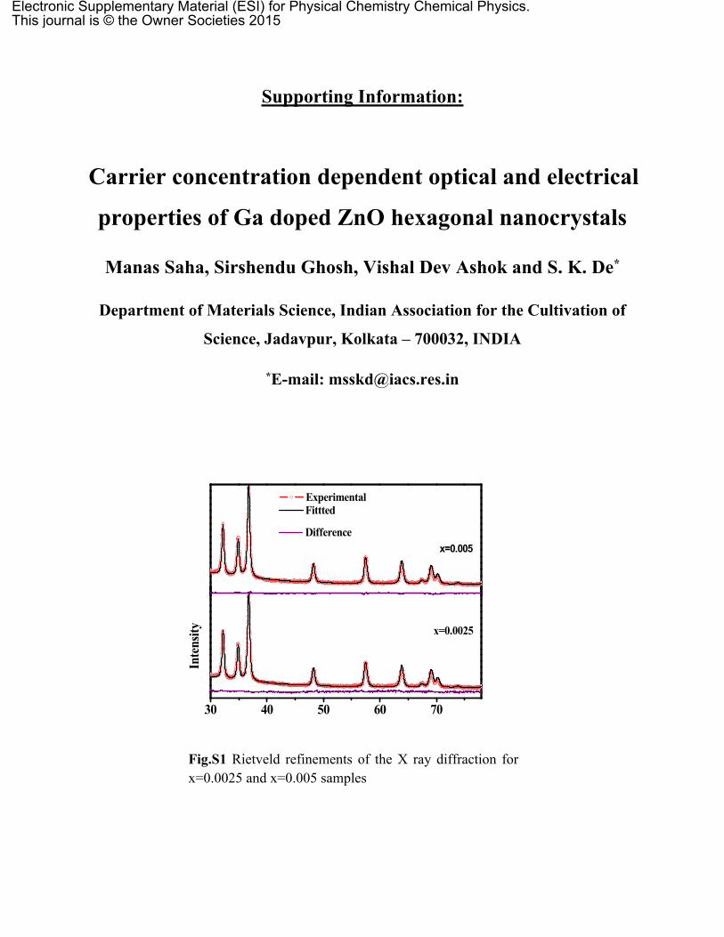
Fig.S1 Rietveld refinements of the X ray diffraction for x=0.0025 and x=0.005 samples
Supporting Information:
Carrier concentration dependent optical and electrical
properties of Ga doped ZnO hexagonal nanocrystals
Manas Saha, Sirshendu Ghosh, Vishal Dev Ashok and S. K. De*
Department of Materials Science, Indian Association for the Cultivation of
Science, Jadavpur, Kolkata – 700032, INDIA
*E-mail: [email protected]
Electronic Supplementary Material (ESI) for Physical Chemistry Chemical Physics.This journal is © the Owner Societies 2015
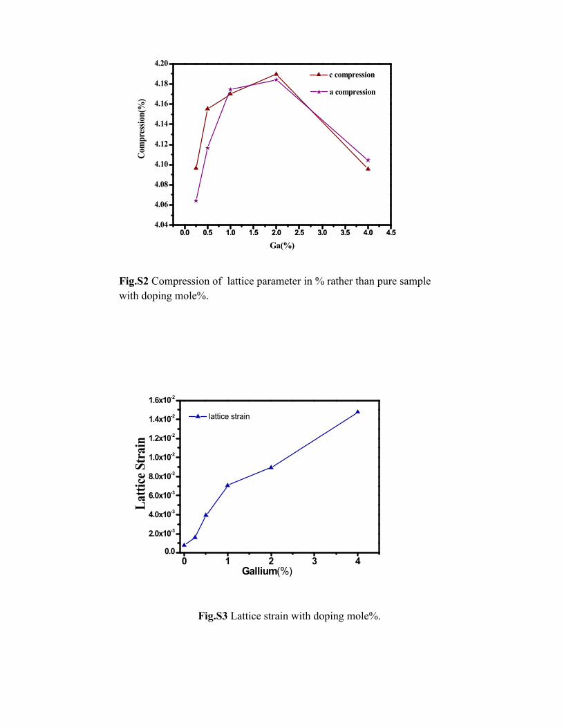
Fig.S2 Compression of lattice parameter in % rather than pure sample with doping mole%.
0.0 0.5 1.0 1.5 2.0 2.5 3.0 3.5 4.0 4.50.0 0.5 1.0 1.5 2.0 2.5 3.0 3.5 4.0 4.54.04
4.06
4.08
4.10
4.12
4.14
4.16
4.18
4.20
c compression
Com
pres
sion(
%)
Ga(%)
a compression
0 1 2 3 40.0
2.0x10⁻³
4.0x10⁻³
6.0x10⁻³
8.0x10⁻³
1.0x10⁻²
1.2x10⁻²
1.4x10⁻²
1.6x10⁻²
Latti
ce S
trai
n
Gallium(%)
lattice strain
Fig.S3 Lattice strain with doping mole%.
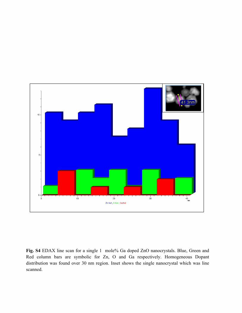
Fig. S4 EDAX line scan for a single 1 mole% Ga doped ZnO nanocrystals. Blue, Green and Red column bars are symbolic for Zn, O and Ga respectively. Homogeneous Dopant distribution was found over 30 nm region. Inset shows the single nanocrystal which was line scanned.

x=0.02
Wavelength(nm.)
ZnO
x= 0.04
300 320 340 360 380 400 420 440 460 480 500
d(A)
/d
x= 0.005
x= 0.01
x= 0.0025
Fig.S5 Differential absorption spectra of pure and doped samples.
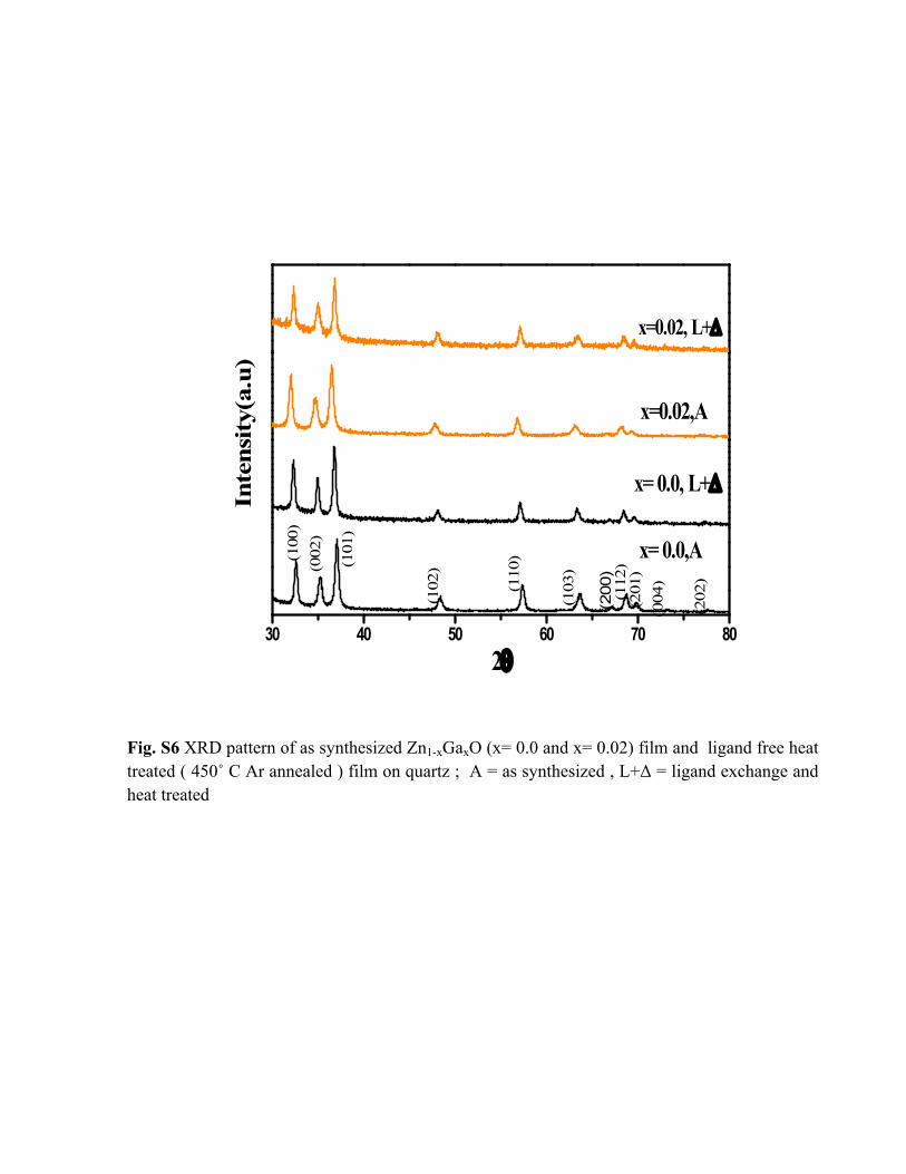
Fig. S6 XRD pattern of as synthesized Zn1-xGaxO (x= 0.0 and x= 0.02) film and ligand free heat treated ( 450˚ C Ar annealed ) film on quartz ; A = as synthesized , L+Δ = ligand exchange and heat treated
30 40 50 60 70 80
x=0.02, L+
Inte
nsit
y(a.
u)
x= 0.0, L+
2
x= 0.0,A(100
)(0
02)
(101
)
(102
)
(110
)
(103
)
(200
)(1
12)
(201
)(0
04)
(202
)
x=0.02,A

Fig. S7
Fig. S7: (a) Cross section SEM image of as-deposited Ga:ZnO thin film. (b) Cross-section view of annealed thin film shows the uniform nature of film.
(b)(a)
(a)
Fig. S8 SEM image of as deposited and annealed film of Zn1-xGaxO. (a) as deposited film of x=0.02 (b) annealed film of x=0.02 (c) as deposited of film x=0.0 and (d) annealed film of x=0.0.
(d)(c)
(a) (b)
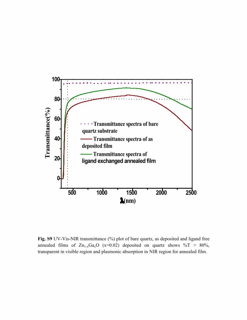
Fig. S9 UV-Vis-NIR transmittance (%) plot of bare quartz, as deposited and ligand free annealed films of Zn1-xGaxO (x=0.02) deposited on quartz shows %T ˃ 80%, transparent in visible region and plasmonic absorption in NIR region for annealed film.
500 1000 1500 2000 2500
0
20
40
60
80
100
Transmittance spectra of ligand exchanged annealed film
Tran
smitt
ance
(%)
(nm)
Transmittance spectra of bare quartz substrate
Transmittance spectra of as deposited film

1200298
0.00 0.01 0.02 0.03 0.040
1000200030004000
50000
60000
70000
Sh
eet R
esis
tanc
e (O
hm/s
q.)
Zn1-xGaxO
Sheet resistance value with error bar
60000
900264650216
3000440
1700470
Fig.S10 Five films prepared under similar conditions for the each composition. Room temperature sheet resistance of Zn1-xGaxO films with error bar for (x=0.0, 0.0025, 0.005, 0.01, 0.02 and 0.04).
-0.6 -0.4 -0.2 0.0 0.2 0.4
2.14
2.16
2.18
2.20
2.22
2.24
2.26
2.28
2.30
2.32
Log(
MIT
Tem
pera
ture
)
Log (concentration of Ga ion in mol%)
slope =1/6.135
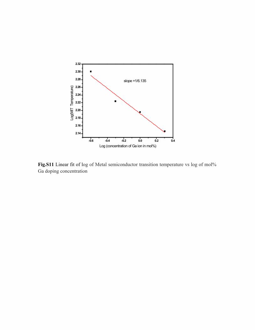
Fig.S11 Linear fit of log of Metal semiconductor transition temperature vs log of mol% Ga doping concentration
50 100 150 200 250 300
0.0
2.0x10⁵
4.0x10⁵
6.0x10⁵
8.0x10⁵
1.0x10⁶
1.2x10⁶
1.4x10⁶
1.6x10⁶
Experimental Fitted
Shee
t res
istan
ce(O
hm/sq
.)
T(K)
Zno
(a)
50 100 150 200 250 300
0
200
400
600
800
1000
1200
1400
Experimental Fitted
Shee
t res
istan
ce (O
hm/sq
.)
T(K)
x=0.005
(c)
50 100 150 200 250 300
0
200
400
600
800
1000
1200
1400
Experimental Fitted
Shee
t res
ista
nce
(Ohm
/sq.
)
T(K)
x=0.01
(d)
50 100 150 200 250 300
0
100
200
300
400
500
600
700 Experimental Fitted
Shee
t res
istan
ce (O
hm/sq
.)
T(K)
x= 0.02
(e)
50 100 150 200 250 300
0
200
400
600
800
1000
1200
1400
1600
1800
Experimental Fitted
Shee
t res
istan
ce(K
ohm
/sq.)
T(K)
x= 0.04
(f)
50 100 150 200 250 300
0
200
400
600
800
1000
1200
1400
1600
Experimental Fitted
Shee
t res
istan
ce(O
hm/sq
.)
T(K)
x= 0.0025
(b)
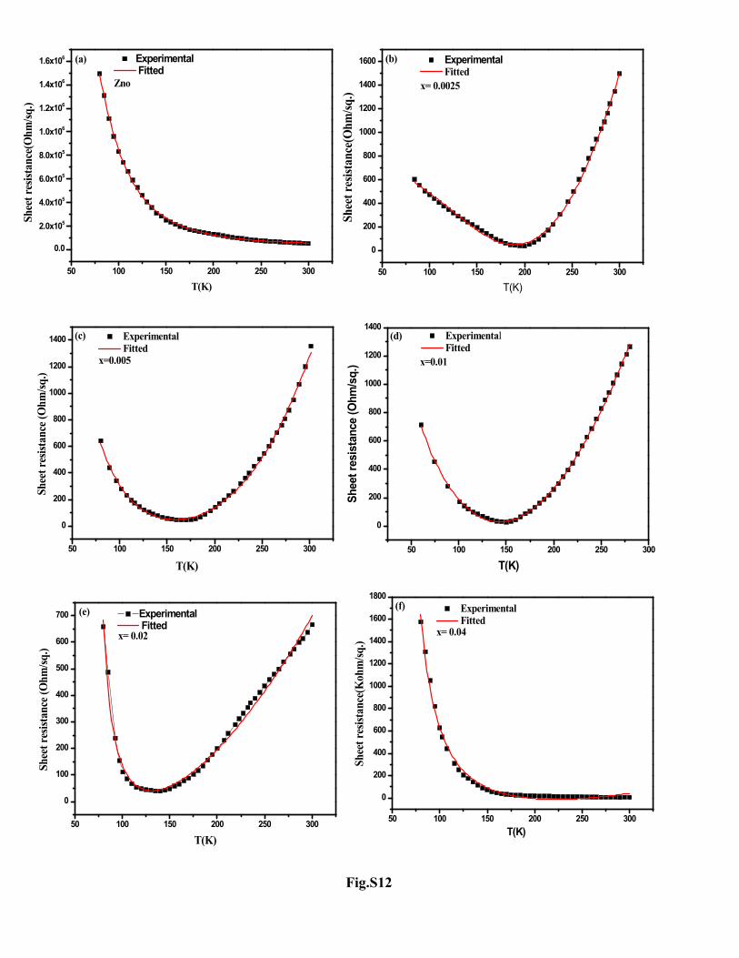
Fig.S12

Table:S1 The fitted parameter for equation (5) with replaced by .𝑎1𝑇𝑝2 𝑎4𝑇
32 + 𝑎1𝑇
𝑝2
Samples a 1 p a 2 a 3 a 4 R0 Adj R
ZnO 6.11967x10⁻¹⁰ 3.8594 4.18795x10⁻⁷ 0.26645 -7.44787x10⁻⁸ -11186.93311 0.99928
X=0.0025 3.19711x10⁻⁷ 2.82618 3.52053x10⁻⁵ 0.07477 -4.51283x10⁻⁶ -8955.79176 0.99789
X=0.005 4.02345x10⁻⁷ 2.46172 1.46435x10⁻⁵ 0.08291 -2.08315x10⁻⁶ -18829.46422 0.99813
X=0.01 4.47102x10⁻⁷ 2.86923 6.02149x10⁻⁵ 0.03869 -5.58869x10⁻⁶ -2873.68986 0.99943
X=0.02 9.77834x10⁻⁶ 2.9912-6.43296x10⁻⁴
0.01063 0 -285.37296 0.9916
X=0.04 2.24156x10⁻⁶ 3.05662-1.45211x10⁻⁴
0.00292 0 -309.94464 0.99263
